


 Loading...
TB7100 base station
Installation and
Operation Manual
MBB-00001-02
Issue 2
December 2005

Tait Contact Information
Tait Radio Communications
Corporate Head Office
Tait Electronics Ltd
P.O. Box 1645
Christchurch
New Zealand
For the address and telephone number of regional offices, refer to the TaitWorld website:
Website: http://www.taitworld.com
Technical Support
For assistance with specific technical issues, contact Technical Support:
E-mail: support@taitworld.com Website: http://support.taitworld.com
To our European customers:
Tait Electronics Limited is an environmentally responsible company which supports waste minimization and material recovery. The European Union’s Waste Electrical and Electronic Equipment Directive requires that this product be disposed of separately from the general waste stream when its service life is over. Please be environmentally responsible and dispose through the original supplier, your local municipal waste “separate collection” service, or contact Tait Electronics Limited.
2 |
TB7100 Installation and Operation Manual |
|
© Tait Electronics Limited December 2005 |

Contents
Preface . . . . . . . . . . . . . . . . . . . . . . . . . . . . . . . . . . . . . . . . . . . . . . . . . . . . . 7
Scope of Manual . . . . . . . . . . . . . . . . . . . . . . . . . . . . . . . . . . . . . . . . . . . . . . . . . . . . 7
Enquiries and Comments . . . . . . . . . . . . . . . . . . . . . . . . . . . . . . . . . . . . . . . . . . . . . . 7
Updates of Manual and Equipment . . . . . . . . . . . . . . . . . . . . . . . . . . . . . . . . . . . . . . . 7
Copyright . . . . . . . . . . . . . . . . . . . . . . . . . . . . . . . . . . . . . . . . . . . . . . . . . . . . . . . . . 7
Disclaimer . . . . . . . . . . . . . . . . . . . . . . . . . . . . . . . . . . . . . . . . . . . . . . . . . . . . . . . . . 7
Document Conventions . . . . . . . . . . . . . . . . . . . . . . . . . . . . . . . . . . . . . . . . . . . . . . . 8
Associated Documentation . . . . . . . . . . . . . . . . . . . . . . . . . . . . . . . . . . . . . . . . . . . . . 8
Publication Record . . . . . . . . . . . . . . . . . . . . . . . . . . . . . . . . . . . . . . . . . . . . . . . . . . 9
1 Introduction . . . . . . . . . . . . . . . . . . . . . . . . . . . . . . . . . . . . . . . . . . . . . . 11
1.1 Frequency Bands . . . . . . . . . . . . . . . . . . . . . . . . . . . . . . . . . . . . . . . . . . . . . . . 12
1.2 RF Output Power . . . . . . . . . . . . . . . . . . . . . . . . . . . . . . . . . . . . . . . . . . . . . . 12
1.3 Power Supply Options . . . . . . . . . . . . . . . . . . . . . . . . . . . . . . . . . . . . . . . . . . . 13
1.4 Mechanical Configurations . . . . . . . . . . . . . . . . . . . . . . . . . . . . . . . . . . . . . . . . 13
1.5 Product Codes . . . . . . . . . . . . . . . . . . . . . . . . . . . . . . . . . . . . . . . . . . . . . . . . . 14
2 Mechanical Description . . . . . . . . . . . . . . . . . . . . . . . . . . . . . . . . . . . . . . 15
2.1 Tray. . . . . . . . . . . . . . . . . . . . . . . . . . . . . . . . . . . . . . . . . . . . . . . . . . . . . . . . . 16
2.2 UI Board . . . . . . . . . . . . . . . . . . . . . . . . . . . . . . . . . . . . . . . . . . . . . . . . . . . . . 16
2.3 Receiver Module . . . . . . . . . . . . . . . . . . . . . . . . . . . . . . . . . . . . . . . . . . . . . . . 17
2.4 Transmitter Module . . . . . . . . . . . . . . . . . . . . . . . . . . . . . . . . . . . . . . . . . . . . . 18
2.5 SI Board. . . . . . . . . . . . . . . . . . . . . . . . . . . . . . . . . . . . . . . . . . . . . . . . . . . . . . 19
2.6 AC Power Supply Unit. . . . . . . . . . . . . . . . . . . . . . . . . . . . . . . . . . . . . . . . . . . 20
3 Functional Description . . . . . . . . . . . . . . . . . . . . . . . . . . . . . . . . . . . . . . . 21
3.1 Receiver Operation . . . . . . . . . . . . . . . . . . . . . . . . . . . . . . . . . . . . . . . . . . . . . 23
3.1.1 RF Hardware . . . . . . . . . . . . . . . . . . . . . . . . . . . . . . . . . . . . . . . . . . 23
3.1.2 Digital Baseband Processing . . . . . . . . . . . . . . . . . . . . . . . . . . . . . . . . 24
3.1.3 Audio Processing and Signalling . . . . . . . . . . . . . . . . . . . . . . . . . . . . . 25
3.2 Transmitter Operation . . . . . . . . . . . . . . . . . . . . . . . . . . . . . . . . . . . . . . . . . . . 26
3.2.1 Audio Processing and Signalling . . . . . . . . . . . . . . . . . . . . . . . . . . . . . 26
3.2.2 Frequency Synthesizer . . . . . . . . . . . . . . . . . . . . . . . . . . . . . . . . . . . . 27
3.2.3 RF Power Amplifier . . . . . . . . . . . . . . . . . . . . . . . . . . . . . . . . . . . . . 30
3.3 User Interface Operation. . . . . . . . . . . . . . . . . . . . . . . . . . . . . . . . . . . . . . . . . . 32
3.4 System Interface Operation . . . . . . . . . . . . . . . . . . . . . . . . . . . . . . . . . . . . . . . . 35
3.4.1 Internal Power Distribution . . . . . . . . . . . . . . . . . . . . . . . . . . . . . . . . 37
3.4.2 Serial Data . . . . . . . . . . . . . . . . . . . . . . . . . . . . . . . . . . . . . . . . . . . . 38
3.4.3 General Purpose IO. . . . . . . . . . . . . . . . . . . . . . . . . . . . . . . . . . . . . . 38
3.4.4 Receiver Audio Processing . . . . . . . . . . . . . . . . . . . . . . . . . . . . . . . . 38
3.4.5 Tone On Idle . . . . . . . . . . . . . . . . . . . . . . . . . . . . . . . . . . . . . . . . . . 38
3.4.6 Transmitter Audio Processing. . . . . . . . . . . . . . . . . . . . . . . . . . . . . . . 38
TB7100 Installation and Operation Manual |
3 |
© Tait Electronics Limited May 2005 |
|
3.4.7 Opto Isolated Keying . . . . . . . . . . . . . . . . . . . . . . . . . . . . . . . . . . . . 39
3.4.8 Relay Output . . . . . . . . . . . . . . . . . . . . . . . . . . . . . . . . . . . . . . . . . . 39
3.4.9 Fan Control . . . . . . . . . . . . . . . . . . . . . . . . . . . . . . . . . . . . . . . . . . . 39
3.4.10 RSSI . . . . . . . . . . . . . . . . . . . . . . . . . . . . . . . . . . . . . . . . . . . . . . . . 39
3.4.11 Receiver Gate. . . . . . . . . . . . . . . . . . . . . . . . . . . . . . . . . . . . . . . . . . 39
3.4.12 Receiver Inhibit . . . . . . . . . . . . . . . . . . . . . . . . . . . . . . . . . . . . . . . . 39
3.5 Fan Operation . . . . . . . . . . . . . . . . . . . . . . . . . . . . . . . . . . . . . . . . . . . . . . . . . 40
4 Installation . . . . . . . . . . . . . . . . . . . . . . . . . . . . . . . . . . . . . . . . . . . . . . . 41
4.1 Personal Safety . . . . . . . . . . . . . . . . . . . . . . . . . . . . . . . . . . . . . . . . . . . . . . . . . 41 4.1.1 Lethal Voltages . . . . . . . . . . . . . . . . . . . . . . . . . . . . . . . . . . . . . . . . . 41 4.1.2 Explosive Environments . . . . . . . . . . . . . . . . . . . . . . . . . . . . . . . . . . 42 4.1.3 Proximity to RF Transmissions . . . . . . . . . . . . . . . . . . . . . . . . . . . . . 42 4.1.4 High Temperatures . . . . . . . . . . . . . . . . . . . . . . . . . . . . . . . . . . . . . . 42
4.2 Equipment Safety . . . . . . . . . . . . . . . . . . . . . . . . . . . . . . . . . . . . . . . . . . . . . . . 42
4.2.1 ESD Precautions . . . . . . . . . . . . . . . . . . . . . . . . . . . . . . . . . . . . . . . . 42
4.2.2 Antenna Load . . . . . . . . . . . . . . . . . . . . . . . . . . . . . . . . . . . . . . . . . . 43
4.2.3 Equipment Grounding . . . . . . . . . . . . . . . . . . . . . . . . . . . . . . . . . . . 43
4.2.4 Installation and Servicing Personnel . . . . . . . . . . . . . . . . . . . . . . . . . . 43
4.3 Regulatory Information . . . . . . . . . . . . . . . . . . . . . . . . . . . . . . . . . . . . . . . . . . 43
4.3.1 Distress Frequencies . . . . . . . . . . . . . . . . . . . . . . . . . . . . . . . . . . . . . 43
4.3.2 FCC Compliance . . . . . . . . . . . . . . . . . . . . . . . . . . . . . . . . . . . . . . . 44
4.3.3 Unauthorised Modifications. . . . . . . . . . . . . . . . . . . . . . . . . . . . . . . . 44
4.3.4 Health, Safety and Electromagnetic Compatibility in Europe. . . . . . . . 44
4.4 Environmental Conditions . . . . . . . . . . . . . . . . . . . . . . . . . . . . . . . . . . . . . . . . 45
4.4.1 Operating Temperature Range . . . . . . . . . . . . . . . . . . . . . . . . . . . . . 45
4.4.2 Humidity . . . . . . . . . . . . . . . . . . . . . . . . . . . . . . . . . . . . . . . . . . . . . 45
4.4.3 Dust and Dirt . . . . . . . . . . . . . . . . . . . . . . . . . . . . . . . . . . . . . . . . . . 45
4.5 Grounding and Lightning Protection. . . . . . . . . . . . . . . . . . . . . . . . . . . . . . . . . 45
4.5.1 Electrical Ground . . . . . . . . . . . . . . . . . . . . . . . . . . . . . . . . . . . . . . . 45
4.5.2 Lightning Ground . . . . . . . . . . . . . . . . . . . . . . . . . . . . . . . . . . . . . . . 45
4.6 Recommended Tools . . . . . . . . . . . . . . . . . . . . . . . . . . . . . . . . . . . . . . . . . . . . 46
4.7 Ventilation. . . . . . . . . . . . . . . . . . . . . . . . . . . . . . . . . . . . . . . . . . . . . . . . . . . . 46
4.7.1 Cabinet and Rack Ventilation . . . . . . . . . . . . . . . . . . . . . . . . . . . . . . 46
4.8 Installing the Base Station . . . . . . . . . . . . . . . . . . . . . . . . . . . . . . . . . . . . . . . . . 49
4.8.1 Unpacking the Equipment. . . . . . . . . . . . . . . . . . . . . . . . . . . . . . . . . 49
4.8.2 Identifying the Mechanical Configuration . . . . . . . . . . . . . . . . . . . . . 49
4.8.3 Power Supply Options . . . . . . . . . . . . . . . . . . . . . . . . . . . . . . . . . . . 50
4.8.4 Setting the AC Mains Input Voltage . . . . . . . . . . . . . . . . . . . . . . . . . 50
4.8.5 Mounting the Base Station . . . . . . . . . . . . . . . . . . . . . . . . . . . . . . . . 51
4.8.6 Cabling . . . . . . . . . . . . . . . . . . . . . . . . . . . . . . . . . . . . . . . . . . . . . . 52
4.8.7 Accessories . . . . . . . . . . . . . . . . . . . . . . . . . . . . . . . . . . . . . . . . . . . . 52
5 Replacing Modules . . . . . . . . . . . . . . . . . . . . . . . . . . . . . . . . . . . . . . . . . |
53 |
5.1 Removing the Base Station and Opening the Tray. . . . . . . . . . . . . . . . . . . . . . . 54
5.2 Replacing the UI Board . . . . . . . . . . . . . . . . . . . . . . . . . . . . . . . . . . . . . . . . . . 55
5.3 Replacing the Receiver Module . . . . . . . . . . . . . . . . . . . . . . . . . . . . . . . . . . . . 56
5.4 Replacing the Transmitter Module . . . . . . . . . . . . . . . . . . . . . . . . . . . . . . . . . . 57
4 |
TB7100 Installation and Operation Manual |
|
© Tait Electronics Limited May 2005 |
5.5 Replacing the SI Board . . . . . . . . . . . . . . . . . . . . . . . . . . . . . . . . . . . . . . . . . . . 58
5.6 Replacing the Transmitter and Receiver Fans . . . . . . . . . . . . . . . . . . . . . . . . . . 59
5.7 Replacing the Fan Power Board . . . . . . . . . . . . . . . . . . . . . . . . . . . . . . . . . . . . 60
5.8 Replacing the Temperature Sensor Board . . . . . . . . . . . . . . . . . . . . . . . . . . . . . 60
5.9 Replacing the AC Power Supply Unit, Fan and Filter Module . . . . . . . . . . . . . . 61
5.10 Replacing the Speaker . . . . . . . . . . . . . . . . . . . . . . . . . . . . . . . . . . . . . . . . . . . 62
5.11 Final Reassembly . . . . . . . . . . . . . . . . . . . . . . . . . . . . . . . . . . . . . . . . . . . . . . . 63
6 Connections . . . . . . . . . . . . . . . . . . . . . . . . . . . . . . . . . . . . . . . . . . . . . . 65
6.1 External Connectors . . . . . . . . . . . . . . . . . . . . . . . . . . . . . . . . . . . . . . . . . . . . . 66
6.2 Internal Connectors . . . . . . . . . . . . . . . . . . . . . . . . . . . . . . . . . . . . . . . . . . . . . 71
6.2.1 Transmitter and Receiver Connectors . . . . . . . . . . . . . . . . . . . . . . . . 71
6.2.2 SI Board Connectors . . . . . . . . . . . . . . . . . . . . . . . . . . . . . . . . . . . . . 73
6.2.3 UI Board Connectors . . . . . . . . . . . . . . . . . . . . . . . . . . . . . . . . . . . . 75
7 Preparation for Operation. . . . . . . . . . . . . . . . . . . . . . . . . . . . . . . . . . . . . 77
7.1 Introduction . . . . . . . . . . . . . . . . . . . . . . . . . . . . . . . . . . . . . . . . . . . . . . . . . . . 77
7.2 Mode of Operation. . . . . . . . . . . . . . . . . . . . . . . . . . . . . . . . . . . . . . . . . . . . . . 77
7.3 Line-controlled Base . . . . . . . . . . . . . . . . . . . . . . . . . . . . . . . . . . . . . . . . . . . . . 78
7.3.1 Test Equipment Required . . . . . . . . . . . . . . . . . . . . . . . . . . . . . . . . . 78
7.3.2 Test Equipment Setup . . . . . . . . . . . . . . . . . . . . . . . . . . . . . . . . . . . . 79
7.3.3 Link Settings . . . . . . . . . . . . . . . . . . . . . . . . . . . . . . . . . . . . . . . . . . . 80
7.3.4 Applying Power . . . . . . . . . . . . . . . . . . . . . . . . . . . . . . . . . . . . . . . . 81
7.3.5 Programming . . . . . . . . . . . . . . . . . . . . . . . . . . . . . . . . . . . . . . . . . . 82
7.3.6 Receiver Audio Level Adjustment . . . . . . . . . . . . . . . . . . . . . . . . . . . 83
7.3.7 Receiver Functional Testing . . . . . . . . . . . . . . . . . . . . . . . . . . . . . . . 84
7.3.8 Transmitter Audio Level Adjustment . . . . . . . . . . . . . . . . . . . . . . . . . 85
7.3.9 Transmitter Functional Testing . . . . . . . . . . . . . . . . . . . . . . . . . . . . . 86
7.4 Talk Through Repeater . . . . . . . . . . . . . . . . . . . . . . . . . . . . . . . . . . . . . . . . . . 88
7.4.1 Test Equipment Required . . . . . . . . . . . . . . . . . . . . . . . . . . . . . . . . . 88
7.4.2 Test Equipment Setup . . . . . . . . . . . . . . . . . . . . . . . . . . . . . . . . . . . . 89
7.4.3 Link Settings . . . . . . . . . . . . . . . . . . . . . . . . . . . . . . . . . . . . . . . . . . . 89
7.4.4 Applying Power . . . . . . . . . . . . . . . . . . . . . . . . . . . . . . . . . . . . . . . . 90
7.4.5 Programming . . . . . . . . . . . . . . . . . . . . . . . . . . . . . . . . . . . . . . . . . . 90
7.4.6 Audio Level Adjustment . . . . . . . . . . . . . . . . . . . . . . . . . . . . . . . . . . 91
7.4.7 Talk Through Repeater Functional Testing . . . . . . . . . . . . . . . . . . . . 91
7.4.8 Alternate Talk Through Repeater Configuration . . . . . . . . . . . . . . . . 92
7.5 RF Modem . . . . . . . . . . . . . . . . . . . . . . . . . . . . . . . . . . . . . . . . . . . . . . . . . . . 93 7.5.1 Test Equipment Required . . . . . . . . . . . . . . . . . . . . . . . . . . . . . . . . . 93 7.5.2 Test Equipment Setup . . . . . . . . . . . . . . . . . . . . . . . . . . . . . . . . . . . . 94 7.5.3 Link Settings . . . . . . . . . . . . . . . . . . . . . . . . . . . . . . . . . . . . . . . . . . . 94 7.5.4 Applying Power . . . . . . . . . . . . . . . . . . . . . . . . . . . . . . . . . . . . . . . . 95 7.5.5 Programming . . . . . . . . . . . . . . . . . . . . . . . . . . . . . . . . . . . . . . . . . . 96 7.5.6 Audio Level Adjustment . . . . . . . . . . . . . . . . . . . . . . . . . . . . . . . . . . 96 7.5.7 Programming for FFSK Operation . . . . . . . . . . . . . . . . . . . . . . . . . . . 96 7.5.8 Programming for THSD Operation . . . . . . . . . . . . . . . . . . . . . . . . . . 98 7.5.9 Verification . . . . . . . . . . . . . . . . . . . . . . . . . . . . . . . . . . . . . . . . . . . 100
TB7100 Installation and Operation Manual |
5 |
© Tait Electronics Limited May 2005 |
|
7.6 Data Repeater . . . . . . . . . . . . . . . . . . . . . . . . . . . . . . . . . . . . . . . . . . . . . . . . 101
7.6.1 Link Settings. . . . . . . . . . . . . . . . . . . . . . . . . . . . . . . . . . . . . . . . . . 102
7.6.2 Applying Power . . . . . . . . . . . . . . . . . . . . . . . . . . . . . . . . . . . . . . . 103
7.6.3 Programming . . . . . . . . . . . . . . . . . . . . . . . . . . . . . . . . . . . . . . . . . 103
7.6.4 Audio Level Adjustment . . . . . . . . . . . . . . . . . . . . . . . . . . . . . . . . . 103
7.6.5 Data Repeater Functional Testing . . . . . . . . . . . . . . . . . . . . . . . . . . 104
7.7 TaitNet Trunking . . . . . . . . . . . . . . . . . . . . . . . . . . . . . . . . . . . . . . . . . . . . . 104
7.8 Programmable Features. . . . . . . . . . . . . . . . . . . . . . . . . . . . . . . . . . . . . . . . . . 105
7.8.1 Connecting to the PC . . . . . . . . . . . . . . . . . . . . . . . . . . . . . . . . . . . 105
7.8.2 TB7100 Programming Application . . . . . . . . . . . . . . . . . . . . . . . . . 105
7.8.3 Mandatory Settings . . . . . . . . . . . . . . . . . . . . . . . . . . . . . . . . . . . . . 107
7.8.4 User-defined Settings . . . . . . . . . . . . . . . . . . . . . . . . . . . . . . . . . . . 108
7.8.5 Recommended Settings. . . . . . . . . . . . . . . . . . . . . . . . . . . . . . . . . . 112
7.8.6 Function Keys. . . . . . . . . . . . . . . . . . . . . . . . . . . . . . . . . . . . . . . . . 113
7.9 Additional Settings . . . . . . . . . . . . . . . . . . . . . . . . . . . . . . . . . . . . . . . . . . . . . 115
7.10 Adding Subaudible Signalling . . . . . . . . . . . . . . . . . . . . . . . . . . . . . . . . . . . . . 115
7.10.1 Enabling Subaudible Signalling . . . . . . . . . . . . . . . . . . . . . . . . . . . . 115
7.10.2 Testing Subaudible Signalling . . . . . . . . . . . . . . . . . . . . . . . . . . . . . 116
7.10.3 Multiple Subaudible Tones . . . . . . . . . . . . . . . . . . . . . . . . . . . . . . . 117
7.11 Soft Off (Tx Tail Time) . . . . . . . . . . . . . . . . . . . . . . . . . . . . . . . . . . . . . . . . . 118
7.11.1 Link Settings. . . . . . . . . . . . . . . . . . . . . . . . . . . . . . . . . . . . . . . . . . 118
7.12 Tone On Idle (TOI). . . . . . . . . . . . . . . . . . . . . . . . . . . . . . . . . . . . . . . . . . . . 118
7.12.1 Link Settings. . . . . . . . . . . . . . . . . . . . . . . . . . . . . . . . . . . . . . . . . . 119
7.13 Fan Operation . . . . . . . . . . . . . . . . . . . . . . . . . . . . . . . . . . . . . . . . . . . . . . . . 120
7.13.1 Link Settings. . . . . . . . . . . . . . . . . . . . . . . . . . . . . . . . . . . . . . . . . . 120
7.14 Channel ID . . . . . . . . . . . . . . . . . . . . . . . . . . . . . . . . . . . . . . . . . . . . . . . . . . 122
7.14.1 Link Settings. . . . . . . . . . . . . . . . . . . . . . . . . . . . . . . . . . . . . . . . . . 122
7.15 Relay Polarity . . . . . . . . . . . . . . . . . . . . . . . . . . . . . . . . . . . . . . . . . . . . . . . . 123
7.15.1 Link Settings. . . . . . . . . . . . . . . . . . . . . . . . . . . . . . . . . . . . . . . . . . 123
7.16 Channel Increment and Decrement by Function Keys . . . . . . . . . . . . . . . . . . . 123
7.17 Carrier Wave Identification (CWID). . . . . . . . . . . . . . . . . . . . . . . . . . . . . . . . 124 7.17.1 Station ID. . . . . . . . . . . . . . . . . . . . . . . . . . . . . . . . . . . . . . . . . . . . 124 7.17.2 Station ID 2/Message . . . . . . . . . . . . . . . . . . . . . . . . . . . . . . . . . . . 124 7.17.3 Tone Frequency . . . . . . . . . . . . . . . . . . . . . . . . . . . . . . . . . . . . . . . 124 7.17.4 ID Repeat Time . . . . . . . . . . . . . . . . . . . . . . . . . . . . . . . . . . . . . . . 124 7.17.5 Speed (Words per Minute) . . . . . . . . . . . . . . . . . . . . . . . . . . . . . . . 124 7.17.6 Wait Period after Loss of COR/COS/CTCSS Input Before IDing . . 124 7.17.7 Transmit Key-Up Delay . . . . . . . . . . . . . . . . . . . . . . . . . . . . . . . . . 124 7.17.8 Transmit Time Out Time . . . . . . . . . . . . . . . . . . . . . . . . . . . . . . . . 125 7.17.9 Transmit PTT Drop Out Time . . . . . . . . . . . . . . . . . . . . . . . . . . . . 125 7.17.10Output Control . . . . . . . . . . . . . . . . . . . . . . . . . . . . . . . . . . . . . . . 125
8 Maintenance Guide . . . . . . . . . . . . . . . . . . . . . . . . . . . . . . . . . . . . . . . . .127
Glossary. . . . . . . . . . . . . . . . . . . . . . . . . . . . . . . . . . . . . . . . . . . . . . . . . . . .129 Directive 1999/5/EC Declaration of Conformity . . . . . . . . . . . . . . . . . . . . . . . .141
6 |
TB7100 Installation and Operation Manual |
|
© Tait Electronics Limited May 2005 |

Preface
Scope of Manual
Welcome to the TB7100 Installation and Operation Manual. This manual provides information on installing and operating the TB7100 base station. Also included in this manual are a high-level circuit description, a functional description and a maintenance guide.
Enquiries and Comments
If you have any enquiries regarding this manual, or any comments, suggestions and notifications of errors, please contact Technical Support (refer to “Tait Contact Information” on page 2).
Updates of Manual and Equipment
In the interests of improving the performance, reliability or servicing of the equipment, Tait Electronics Limited reserves the right to update the equipment or this manual or both without prior notice.
Copyright
All information contained in this manual is the property of
Tait Electronics Limited. All rights are reserved. This manual may not, in whole or in part, be copied, photocopied, reproduced, translated, stored, or reduced to any electronic medium or machine-readable form, without prior written permission from Tait Electronics Limited.
Disclaimer
There are no warranties extended or granted by this manual.
Tait Electronics Limited accepts no responsibility for damage arising from use of the information contained in the manual or of the equipment and software it describes. It is the responsibility of the user to ensure that use of such information, equipment and software complies with the laws, rules and regulations of the applicable jurisdictions.
TB7100 Installation and Operation Manual |
7 |
© Tait Electronics Limited December 2005 |
|

Document Conventions
“File > Open” means “click File on the menu bar, then click Open on the list of commands that pops up”. “Channel Setup > Channels > Detailed” means “in the navigation pane find the Channel Setup group, and select Channels from it, on the Channels page select the Detailed tab”.
Within this manual, four types of alerts are given to the reader: Warning, Caution, Important and Note. The following paragraphs illustrate each type of alert and its associated symbol.
Warning!! This alert is used when there is a potential risk of death or serious injury.
Caution This alert is used when there is a risk of minor or moderate injury to people.
Important This alert is used to warn about the risk of equipment damage or malfunction.
Note This alert is used to highlight information that is required to ensure procedures are performed correctly.
Associated Documentation
The following associated documentation is available for this product:
■MBB-00002-xx TB7100 Specifications Manual
■MBB-00003-xx TB7100 Installation Guide
■MBB-00005-xx TB7100 Service Manual
■MBA-00013-xx TBA0STU/TBA0STP Calibration and Test Unit
Operation Manual
The characters xx represent the issue number of the documentation.
All available documentation is provided on the CD (406-00047-xx) supplied with the base station. Updates may also be published on the Tait support website.
Technical notes are published from time to time to describe applications for Tait products, to provide technical details not included in manuals, and to offer solutions for any problems that arise.
8 |
TB7100 Installation and Operation Manual |
|
© Tait Electronics Limited December 2005 |
Publication Record
Issue |
Publication Date |
Description |
|
|
|
1 |
May 2005 |
First release |
|
|
|
2 |
December 2005 |
Internal AC power supply, A4 and D1 bands |
|
|
added. |
|
|
|
TB7100 Installation and Operation Manual |
9 |
© Tait Electronics Limited December 2005 |
|
10 |
TB7100 Installation and Operation Manual |
|
© Tait Electronics Limited December 2005 |
1 Introduction
Figure 1.1 TB7100 base stations
Configuration with provision for internal AC power supply*
Configuration without provision for internal AC power supply*
*cover removed
The TB7100 is a software and hardware link-configured base station which is designed for operation in a large variety of standard frequency ranges. It makes extensive use of digital and DSP technology. Many operating parameters such as channel spacing, audio bandwidth and signalling are controlled by software.
This manual includes the information required for installing and operating the base station.
This section describes the different options available for:
■frequency bands
■RF output power
■power supply
■mechanical configurations
■product codes
For specifications, refer to the specifications manual or the area on the
TaitWorld website reserved for TB7100 products.
TB7100 Installation and Operation Manual |
Introduction |
11 |
© Tait Electronics Limited December 2005 |
|
|

1.1Frequency Bands
The base station is available in the following frequency bands:
■66 to 88MHz (A4)
■136 to 174MHz (B1)
■216 to 266 MHz (D1)
■400 to 470MHz (H5)
■450 to 530MHz (H6)
■450 to 520MHz (H7)
The RF band of the base station is implemented by the frequency band of the transmitter and receiver modules.
1.2RF Output Power
The base station is available with 25W and 50W/40W RF output power. The RF output power options are implemented by different transmitter and receiver modules.
The 25W base station is available in the following frequency bands:
■A4
■B1
■D1
■H5
■H6
The 50W/40W base station is available in the following frequency bands:
■ B1 (50W)
■H5 (40W)
■H7 (40W)
12 |
Introduction |
TB7100 Installation and Operation Manual |
|
|
© Tait Electronics Limited December 2005 |

1.3Power Supply Options
The base station is available with or without an internal AC power supply.
All base stations have an external DC input power connector which is used as main power supply when no internal AC power supply is fitted.
When the internal AC power supply is fitted, the DC input can be used as a DC backup power option. In case of AC mains failure the base station will automatically and seamlessly switch to DC power input.
If no internal AC power supply is fitted, an external Tait T809-10-87xx power supply can be used to supply the DC voltage required.
Warning!! The internal AC power supply unit contains voltages that may be lethal. Refer to the ratings label on the rear of the base station. The internal AC power supply contains no user-servicable parts.
Important Wrong mains voltage! Before connecting to the AC power connector, ensure that the internal 115V/230V voltage mains selector switch is set to the correct mains voltage.
1.4Mechanical Configurations
The base station is available in two different mechanical configurations— with or without provision for an internal AC power supply unit.
The mechanical configuration with provision for an internal AC power supply has the following distinguishing features:
■larger air intake on the right-hand side of the front panel
■provision for AC connector on the left-hand side of the rear panel (refer to Figure 1.1 on page 11)
■ground point on the right-hand side of the rear panel rather than on the left-hand side
■different SI board and internal cables.
The mechanical configuration without provision for an internal AC power supply unit cannot be upgraded with an internal AC power supply unit.
The product codes of the base station (see below) do not distinguish between the mechanical configurations.
TB7100 Installation and Operation Manual |
Introduction |
13 |
© Tait Electronics Limited December 2005 |
|
|
1.5Product Codes
This section describes the product codes used to identify products of the
TB7100 base station product line.
The product codes of the TB7100 base station product line has the format:
TBBaabb-cde-ff
where:
■aa identifies the frequency band of the receiver:
A4=66 to 88MHz, B1=136 to 174MHz, D1=216 to 266 MHz, H5=400 to 470MHz, H6=450 to 530MHz, H7=450 to 520MHz
■bb identifies the frequency band of the transmitter:
A4=66 to 88MHz, B1=136 to 174MHz, D1=216 to 266 MHz, H5=400 to 470MHz, H6=450 to 530MHz, H7=450 to 520MHz
■c identifies the RF output power and digital architecture: A=25W, level-1 digital architecture
B=35W to 50W, level-1 digital architecture C=25W, level-2 digital architecture D=35W to 50W, level-2 digital architecture E=25W, level-3 digital architecture F=35W to 50W, level-3 digital architecture
■d identifies the power supply option: 0=DC only
1=internal AC power supply unit, factory preset to 115VAC 2=internal AC power supply unit, factory preset to 230VAC
■e identifies the AC power cable: 1 = Australia/New Zealand
2 = United Kingdom
3 = Europe
4 = USA
■ff identifies base station options: 00=no options
14 |
Introduction |
TB7100 Installation and Operation Manual |
|
|
© Tait Electronics Limited December 2005 |

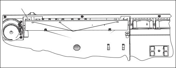
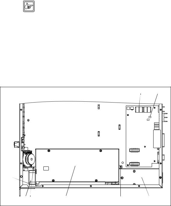
2 Mechanical Description
Overview |
The base station consists of the following main modules: |
■tray b
■UI board (user interface) d
■receiver module h
■transmitter module i
■SI board (system interface) 1)
■internal AC power supply unit 1@ (if fitted).
Figure 2.1 Parts of the base station (configuration with internal AC power supply unit shown)
|
|
f |
g |
|
|
h |
|
|
|
|
|
|
e |
|
|
|
d |
|
|
|
|
|
i |
|
c |
|
j |
|
|
|
|
b |
|
|
|
1# |
1@ |
|
|
|
1! |
|
1) |
All modules and boards are mounted from above into the 1U tray b. The modules are secured by screws or clips into standoffs on the tray chassis, and are easily removed for replacement.
The base station includes two cooling fans f and a fan duct e in front of the receiver and transmitter modules, a speaker c mounted behind the front panel, a fan power board g mounted on the fan duct, and a temperature sensor board j mounted on the heatsink of the transmitter module i.
If the internal AC power supply unit 1@ is fitted, the base station includes an additional fan 1# and an AC filter module 1!.
The modules and components are interconnected by looms and cables.
TB7100 Installation and Operation Manual |
Mechanical Description |
15 |
© Tait Electronics Limited December 2005 |
|
|
2.1Tray
The 1U tray consists of a mild steel folded chassis and a flat cover (not shown) which is fastened to the chassis with 15 Torx T10 screws. The tray can be fitted into a standard 19 inch rack or cabinet using the two rack mounting brackets.
The front panel has holes to accommodate the controls and the microphone/programming connector of the UI board.
The rear panel has holes to accommodate the connectors and the fuse holder of the SI board, the antenna connectors, and a ground terminal.
For more information on the connections, refer to “Connections” on page 65.
2.2UI Board
The UI board is mounted behind the front panel with three Torx T10 screws c and two spring clips D. The UI board is connected to the transmitter and receiver modules via the two Micro-MaTch connectors e and the two UI cables (not shown). The UI board also has a speaker connector b.
A volume knob is fitted to the shaft of the volume-control potentiometer.
Figure 2.2 |
UI board |
|
|
b |
|
|
c |
e |
|
|
|
|
d |
|
Cables not shown. |
|
|
16 |
Mechanical Description |
TB7100 Installation and Operation Manual |
|
|
© Tait Electronics Limited December 2005 |

2.3Receiver Module
The receiver module is mounted in the front left of the tray with five Torx T10 screws g.
The receiver module is a printed circuit board in SMT design with components on the top and bottom sides. A digital board is reflow-soldered to the receiver. Most components are shielded by metal cans.
There are different boards for each frequency band and each RF output power configuration.
The RF b, DC power c, auxiliary d, and user interface f connectors are located on the bottom side of the board. The internal options connector e and a factory connector (not shown) for factory use are located on the top side of the board.
For compliance reasons, there are different variants of the receiver module for use in the 25W and 50W/40W base stations. The 25W version has a white DC power connector C and the 50W/40W version has a black DC power connector.
For more information on the connectors, refer to “Connections” on page 65.
Figure 2.3 Receiver module
b |
c |
d |
|
|
e |
|
|
g |
|
|
g |
g |
f |
|
TB7100 Installation and Operation Manual |
Mechanical Description |
17 |
© Tait Electronics Limited December 2005 |
|
|
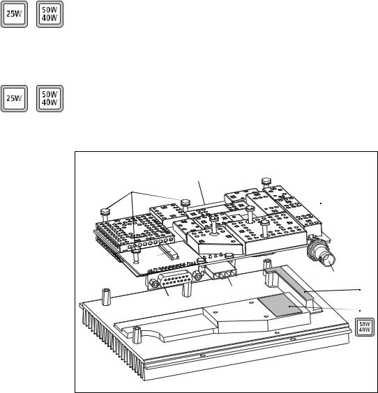
2.4Transmitter Module
The transmitter module consisting of a transmitter board f mounted on a purpose-designed heatsink 1) is mounted in the left rear of the tray with four Torx T10 screws (not shown).
The transmitter board is a printed circuit board in SMT design with components on the top and bottom sides. A digital board is reflow-soldered to the board. Most components are shielded by metal cans. There are different boards for each frequency band and each RF output power configuration.
The RF b, DC power c, auxiliary d, and user interface f connectors are located on the bottom side of the board. The internal options connector e and a factory connector (not shown) for factory use are located on the top side of the board.
The 50W/40W version has a black DC power connector C and the 25W version has a white DC power connector. For more information on the connectors, refer to “Connections” on page 65.
The board f is mounted to the heatsink 1) with seven Torx T10 screws f and g.
An L-shaped gap pad i and (with the 50W/40W version) a rectangular gap pad j are fitted between the board f and the heatsink 1) to improve heat transfer.
Figure 2.4 Transmitter module
f |
g |
|
|
h |
|
|
g |
e |
|
|
b |
c |
i |
D |
j |
|
|
|
1) |
18 |
Mechanical Description |
TB7100 Installation and Operation Manual |
|
|
© Tait Electronics Limited December 2005 |

2.5SI Board
The SI board is mounted in the rear right of the tray with two Torx T10 screws 1), one Pozidriv screw j, and two spring clips 1!.
The SI board has the following external connectors:
■13.8V DC power connector (labelled 12V DC) b
■system connector (labelled SYSTEM) c
■serial data connector (labelled IOIOI) D.
The SI board has the following internal connectors:
■two system interface connectors e (to transmitter and receiver)
■one DC input connector h, if fitted (from internal AC power supply)
■one DC output connector i (to transmitter and receiver)
■fan control connector f (to fan power board on fan duct)
■temperature control connector g (to temperature sensor on transmitter heatsink).
For more information on the connectors, refer to “Connections” on
|
|
page 65. |
|
|
|
Figure 2.5 |
SI board |
|
|
|
|
|
|
b |
c |
d |
|
|
1) |
|
|
|
1) |
|
|
|
|
|
|
|
i |
|
|
|
|
|
|
|
|
|
j |
|
h |
|
|
|
|
|
g |
|
|
|
|
|
f |
1! |
|
e |
1! |
TB7100 Installation and Operation Manual |
Mechanical Description |
19 |
© Tait Electronics Limited December 2005 |
|
|
2.6AC Power Supply Unit
The base station may be fitted with an internal AC power supply unit f, an AC filter module d, and an additional fan g.
The AC filter module has a standard AC connector that fits into a provision on the rear of the tray. The AC filter module slides into securing tabs on the tray floor and is held in place by the AC power supply unit.
Note Mechanical configurations without the provision for a standard AC connector cannot be upgraded with the internal AC power supply unit.
The AC power supply unit is held in place by two screws e. The fan is attached to the AC power supply unit by two screws h.
The AC power supply unit is connected to the AC filter module via a cable connector (not shown).
The DC output of the AC power supply unit is connected to the SI board b. The AC power supply unit also has a cable to provide a mains failure signal to the SI board c. In case of a mains failure, this signal will cause the power circuitry on the SI board to switch to DC external input.
Figure 2.6 AC power supply unit, filter module and fan
|
|
b |
c |
h |
|
|
|
g e |
f |
e |
d |
20 |
Mechanical Description |
TB7100 Installation and Operation Manual |
|
|
© Tait Electronics Limited December 2005 |
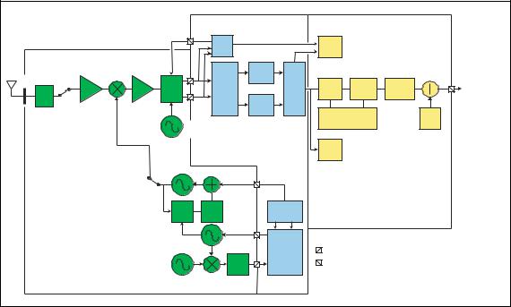
3 Functional Description
This section describes some principles of the base station operation.
Figure 3.1 shows the high-level block diagram of the base station.
Figure 3.1 Base station high-level block diagram
Ground |
Tx/Ant |
Rx |
|
DC Input |
System |
Serial Data |
AC Input |
||
Point |
Connector |
Connector |
|
||||||
Fuse |
Connector |
Connector |
Connector |
Connector |
|||||
|
|
|
|||||||
|
RF |
|
|
|
|
|
|
|
|
|
Temperature |
|
|
|
|
|
InputFilter |
Module |
|
|
Sensor |
|
|
|
SI Board |
|
|||
|
|
|
|
|
|
||||
Transmitter |
Internal power |
|
|
|
|
|
|||
|
|
|
|
|
AC |
|
|||
Module |
|
|
|
|
|
|
|
||
|
|
|
|
|
|
|
|
||
|
Transmitter/SI |
|
|
|
Internal power |
|
|
||
|
|
|
|
|
|
|
|
||
|
RF |
|
|
|
signal |
|
|
|
|
|
|
|
|
Mainsfail |
|
|
|
||
|
|
|
|
|
|
|
|
||
Receiver |
Internal power |
|
|
|
|
AC |
|
|
|
Module |
|
|
|
|
|
|
|||
|
|
|
|
|
Power Supply |
|
|||
|
|
|
|
|
|
|
|||
|
|
|
|
|
|
Unit |
|
|
|
|
Receiver/SI |
|
|
|
|
115V/230V |
|
|
|
|
|
|
|
|
|
Selector |
|
|
|
|
|
|
|
|
|
Switch |
|
|
|
Fan Power |
|
|
|
|
|
|
|
|
|
Board |
|
|
|
|
|
|
|
|
|
Fan |
Fan |
|
|
|
|
|
|
|
|
Internal power |
UI Board |
|
|
|
|
|
|||
|
UI/Receiver |
|
|
|
|
|
|||
|
|
|
|
|
|
|
|
||
UI/Transmitter |
|
|
|
Speaker |
Fan |
|
|||
|
|
|
|
|
|
||||
|
Prog/Mic |
|
|
|
|
|
|
|
|
|
Connector |
|
|
|
|
|
|
|
|
TB7100 Installation and Operation Manual |
Functional Description |
21 |
© Tait Electronics Limited December 2005 |
|
|
Frequency Bands
and Sub-bands
The block diagram illustrates the main inputs and outputs for power, RF and control signals, as well as the interconnection between modules:
■program data and audio from the PROG/MIC socket on the UI board to and from the transmitter and receiver modules
■audio and signalling from the SYSTEM connector to and from the transmitter and receiver modules
■RS-232 data from the serial data connector (IOIOI) to and from the transmitter and receiver modules
■fan power and control from the SI board
■power distribution from the AC and DC power input connectors to the transmitter and receiver modules, and from the receiver module to the UI board.
The circuitry of the individual modules that make up the base station is described in more detail in the following sections.
The circuitry of the transmitter and receiver modules is similar for all frequency bands and is therefore covered by a single description in this manual. Where the circuitry differs between bands, separate descriptions are provided for each frequency band. For more information on frequency bands, refer to the specifications manual.
RS-232 Signals |
External data communications all occur directly between the connected |
|
computer (or other electrical equipment) and the transmitter and receiver |
|
modules over the RS-232 serial lines. |
Fan Signals |
The power and ground signals for the fans are routed from the SI board to |
|
the fans behind the front panel. These signals are electrically isolated from |
|
all other system signals to ensure fan noise is not transferred to other sensitive |
|
system components. |
|
If there is a fault in the fan circuitry, the transmitter module is protected from |
|
overheating by its internal foldback circuitry. |
Speaker Signal |
Received audio is sent from the receiver module to the UI board. |
|
The volume is controlled by the volume potentiometer on the UI board. |
|
The audio signal is routed through the UI board to the speaker for |
|
monitoring purposes. |
Power and Ground |
The SI board provides power to the transmitter and receiver modules. |
|
The receiver modules provides power to the UI board. |
22 |
Functional Description |
TB7100 Installation and Operation Manual |
|
|
© Tait Electronics Limited December 2005 |
3.1Receiver Operation
Parts of Receiver The main circuit parts of the receiver modules are:
Board
■receiver
■frequency synthesizer
■CODEC (coder-decoder) and audio circuitry
■power supply
■interface circuitry
Software plays a prominent role in the functioning of the radio.
When describing the operation of the radio the software must be included with the above. This is considered further below.
These functional parts are described in detail below.
Figure 3.2 Receiver high-level block diagram
|
|
|
|
|
RX |
|
|
RSSI |
|
|
|
|
|
|
|
|
AGC |
|
|
|
|
|
|
|
|
|
|
|
|
|
|
|
|
|
|
|
|
IF: |
|
|
|
|
Mag. |
|
|
|
|
|
|
|
|
|
|
|
|
|
|
|
|
|
|
UHF: 45.1 MHz |
|
|
|
|
|
|
|
|
|
|
|
VHF: 21.4 MHz |
|
|
|
|
Channel |
|
|
|
|
ANT |
|
|
|
|
|
|
LPF |
|
|
|
|
|
|
|
|
Digital |
|
|
|
|
|
|
|
|
Front |
1st |
Quad |
|
|
FM |
Audio |
De- |
Optional |
System Interface |
|
|
|
down- |
|
||||||||
|
end |
IF |
Demod |
|
|
Demod |
filtering |
emphasis |
processing |
or User Interface |
|
LPF |
|
converter |
|||||||||
|
|
|
|
|
|
|
|
|
|||
|
|
|
|
|
|
|
Channel |
|
|
|
|
|
|
|
|
|
2nd IF: |
|
LPF |
|
|
|
|
|
|
|
|
|
64 kHz |
|
|
Data and signalling |
|
Side |
|
|
|
Phase |
|
Second LO |
|
|
decoders |
|
tones |
||
|
|
locked to |
|
|
|
|
|
|
|
||
|
|
|
UHF: 90.328 MHz |
CUSTOM- |
|
|
|
|
|||
|
|
TCXO |
|
VHF: 42.928 MHz |
|
|
|
|
|||
|
|
|
|
|
|
|
LOGIC |
Squelch |
|
|
|
|
|
|
|
|
|
|
|
|
|
|
|
|
|
|
|
|
|
|
BLOCK |
|
|
DSP |
|
|
|
|
|
|
|
|
|
|
|
|
|
|
|
|
VCO |
|
|
|
|
|
BLOCK |
|
|
|
|
|
|
|
|
|
|
|
|
||
|
|
|
PLL |
Loop |
|
Triple-point |
|
|
|
|
|
|
|
|
filter |
|
Equalisation |
|
|
|
|
||
|
|
|
|
|
|
|
|
|
|
||
HARDWARE BLOCK |
|
VCXO |
|
|
KEY |
|
|
|
|||
|
|
|
|
|
|
|
|
|
|||
|
|
|
|
|
|
|
Frequency |
|
Analogue-to-digital conversion |
||
|
|
|
|
|
|
|
control |
|
|||
|
|
|
|
|
|
|
|
|
|
|
|
|
|
TCXO: |
|
|
Loop |
|
|
Digital-to-analogue conversion |
|||
|
|
|
|
|
filter |
|
|
||||
|
|
13.000 MHz |
|
|
|
NOTES |
|
|
|||
|
|
|
|
|
|
|
|
|
|
||
|
|
|
|
|
|
|
|
(1) |
Noise blanker not shown |
|
|
3.1.1RF Hardware
Front End Circuitry
and First IF
The front-end hardware amplifies and image filters the received RF spectrum, then down-converts the desired channel frequency to a first intermediate frequency IF1 of 45.1MHz (UHF) or 21.4MHz (VHF) where coarse channel filtering is performed. The first LO (local oscillator) signal is obtained from the frequency synthesizer and is injected on the low side of the desired channel frequency for all bands except A4. When receiving the modulation to the frequency synthesizer is muted. The output of the first IF (intermediate frequency) stage is then down-converted using an imagereject mixer to a low IF of 64kHz.
TB7100 Installation and Operation Manual |
Functional Description |
23 |
© Tait Electronics Limited December 2005 |
|
|
Quadrature
Demodulator
Automatic Gain
Control
The LO for the image-reject mixer (quadrature demodulator) is synthesized and uses the TCXO (temperature-compensated crystal oscillator) as a reference. This ensures good centring of the IF filters and more consistent group-delay performance. The quadrature demodulator device has an internal frequency division of 2 so the second LO operates at
2 x (IF1 + 64kHz). The quadrature output from this mixer is fed to a pair of ADCs (analog-to-digital converters) with high dynamic range where it is oversampled at 256kHz and fed to the custom logic device.
The AGC (automatic gain control) is used to limit the maximum signal level applied to the image-reject mixer and ADCs in order to meet the requirements for intermodulation and selectivity performance. Hardware gain control is performed by a variable-gain amplifier within the quadrature demodulator device driven by a 10-bit DAC (digital-to-analog converter). Information about the signal level is obtained from the IQ (in-phase and quadrature) data output stream from the ADCs. The control loop is completed within custom logic. The AGC will begin to reduce gain when the combined signal power of the wanted signal and first adjacent channels is greater than about –70dBm. In the presence of a strong adjacent-channel signal it is therefore possible that the AGC may start acting when the wanted signal is well below –70dBm.
3.1.2Digital Baseband Processing
Custom Logic |
The remainder of the receiver processing up to demodulation is performed |
|
by custom logic. The digitised quadrature signal from the RF hardware is |
|
digitally down-converted to a zero IF, and channel filtering is performed at |
|
base-band. Different filter shapes are possible to accommodate the various |
|
channel spacings and data requirements. These filters provide the bulk of |
|
adjacent channel selectivity for narrow-band operation. The filters have |
|
linear phase response so that good group-delay performance for data is |
|
achieved. The filters also decimate the sample rate down to 48kHz. Custom |
|
logic also performs demodulation, which is multiplexed along with AGC |
|
and amplitude data, and fed via a single synchronous serial port to the DSP. |
|
The stream is demultiplexed and the demodulation data used as an input for |
|
further audio processing. |
Noise Squelch |
The noise squelch process resides in the DSP. The noise content above and |
|
adjacent to the voice band is measured and compared with a preset |
|
threshold. When a wanted signal is present, out-of-band noise content is |
|
reduced and, if below the preset threshold, is indicated as a valid wanted |
|
signal. |
Received Signal
Strength Indication
Received signal strength is measured by a process resident in the DSP. This process obtains its input from the demodulator (value of RF signal magnitude) and from the AGC (value of present gain). With these two inputs and a calibration factor, the RF signal strength at the antenna can be accurately calculated.
24 |
Functional Description |
TB7100 Installation and Operation Manual |
|
|
© Tait Electronics Limited December 2005 |
Calibration |
The following items within the receiver path are calibrated in the Factory: |
|
|
■ front-end tuning |
|
|
■ |
AGC |
|
■ |
noise squelch |
■ RSSI (received signal strength indication)
Information on the calibration of these items is given in the on-line help facility of the calibration application.
3.1.3Audio Processing and Signalling
Audio Processing Raw demodulated data from the receiver is processed within the DSP. The sample rate at this point is 48kHz with signal bandwidth limited only by the IF filtering. Scaling (dependent on the bandwidth of the RF channel) is then applied to normalise the signal level for the remaining audio processing.
The sample rate is decimated to 8kHz and bandpass audio filtering (0.3 to 3kHz) is applied. The base station takes the audio from the receiver mode at Tap R4 by default; this point has no de-emphasis. This tap point can be changed if required, for example, for trunking applications.
Data and Signalling
Decoders
The data and signalling decoders obtain their signals from various points within the audio processing chain. The point used depends on the bandwidth of the decoders and whether de-emphasis is required. Several decoders may be active simultaneously.
Side Tones |
Side tones are summed in at the end of the audio-processing chain. |
|
These are tones that provide some form of alert or give the user confidence |
|
an action has been performed. The confidence tones may be generated in |
|
the receiver. The side-tone level is a fixed proportion (in the order of |
|
–10dB) relative to full scale in the receive path. By default, all audible |
|
indicators are turned off. |
CODEC |
The combined audio and side-tone signal is converted to analog form by a |
|
16-bit DAC with integral anti-alias filtering. This is followed by a |
|
programmable-gain amplifier with a range of 45dB in 1.5dB steps. |
|
The amplifier performs muting. The DAC is part of the same CODEC |
|
device (AD6521). |
Output to Speakers |
The output of the CODEC is fed to an audio power amplifier and to the |
|
UI board via a buffer amplifier. The output configuration of the audio |
|
power amplifier is balanced and drives an internal speaker. The power |
|
delivered to the speaker is limited by its impedance. The speaker has 16Ω |
|
impedance. |
TB7100 Installation and Operation Manual |
Functional Description |
25 |
© Tait Electronics Limited December 2005 |
|
|
3.2Transmitter Operation
Parts of Transmitter The main circuit parts of the transmitter board are:
Board
■transmitter
■frequency synthesizer
■CODEC (coder-decoder) and audio circuitry
■power supply
■interface circuitry
Software plays a prominent role in the functioning of the board.
When describing the operation of the radio the software must be included with the above. This is considered further below.
These functional parts are described in detail below.
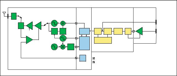
Figure 3.3 Transmitter high-level block diagram
ANT |
HARDWARE BLOCK |
|
CUSTOM |
|
DSP |
|
HARDWARE |
|
||
|
|
|
|
|
||||||
LPF |
|
|
|
LOGIC |
|
BLOCK |
|
BLOCK |
|
|
|
|
VCO |
|
BLOCK |
|
|
|
|
|
|
|
|
|
|
|
|
|
|
|
|
|
|
|
|
|
|
|
|
|
|
|
SYSTEM connector |
Dir. |
Fin |
Drv |
|
|
|
Tap point T8 |
|
|
|
|
Coup. |
/Ex |
|
|
|
|
|
|
|
||
|
|
|
|
|
|
|
|
|
||
|
Bias |
PLL |
Loop |
Triple-point |
Audio |
Pre- |
Optional |
ALC |
Mic |
PROG/MIC connector |
|
filter |
Equalisation |
filtering |
emphasis |
processing |
PGA |
||||
|
|
|
|
|
||||||
|
Pwr |
VCXO |
|
|
Data and signalling |
|
|
|
|
|
|
Crtl |
|
|
Frequency |
encoders |
|
|
|
|
|
|
|
|
|
|
|
|
|
|
|
|
|
|
|
|
control |
|
|
|
|
|
|
|
|
TCXO: |
|
Loop |
|
|
|
|
|
|
|
|
13.000 MHz |
|
filter |
|
|
|
|
|
|
|
|
|
|
|
KEY |
|
|
|
|
|
|
|
|
|
Ramp |
Analog-to-digital conversion |
|
|
|
||
|
|
|
|
control |
|
|
|
|||
|
|
|
|
|
|
|
|
|
|
|
|
|
|
|
|
Digital-to-analog conversion |
|
|
|
||
3.2.1Audio Processing and Signalling
Microphone Input The input to the transmitter path begins at either the SI board or the PROG/MIC connector of the UI board. Only electret-type microphones are supported. The audio input is then applied to tap point T8 on the transmitter board (the tap point is user-selectable).
Analog Processing
of Microphone
Signal
The CODEC (AD6521) performs microphone selection and amplification. The microphone amplifier consists of an amplifier with a fixed gain of 16dB followed by a programmable-gain amplifier with 0dB to 22dB gain.
The amplified microphone signal is converted to a digital stream by a 16-bit ADC with integral anti-alias filtering (0.1 to 3.2kHz). The digital stream is transported to the DSP for further audio processing.
26 |
Functional Description |
TB7100 Installation and Operation Manual |
|
|
© Tait Electronics Limited December 2005 |
Automatic Level
Control
The ALC (automatic level control) follows, and is used to effectively increase dynamic range by boosting the gain of the microphone pre-amplifier under quiet conditions and reducing the gain under noisy acoustic conditions.
The ALC function resides in the DSP and controls the microphone programmable-gain amplifier in the CODEC. The ALC has a fast-attack (about 10ms) and slow-decay (up to 2s) characteristic. This characteristic ensures that the peak signal level is regulated near full scale to maximise dynamic range.
DSP Audio
Processing
The output of the automatic level control provides the input to the DSP audio-processing chain at a sample rate of 8kHz. Optional processing such as encryption or companding is done first if applicable. Pre-emphasis, if required, is then applied. The pre-emphasised signal is hard limited to prevent over deviation, and filtered to remove high-frequency components. The sample rate is then interpolated up to 48kHz and scaled to be suitable for the frequency synthesizer.
Data and Signalling The data and signalling encoders inject their signals into various points Encoders within the audio-processing chain. The injection point depends on the
bandwidth of the encoders and whether pre-emphasis is required.
3.2.2Frequency Synthesizer
Main Parts of |
The frequency synthesizer consists of two main parts: |
Synthesizer |
■ FCL (frequency control loop) |
|
|
|
■ RF PLL (phase-locked loop) |
|
The FCL and RF PLL are described briefly below. Note that patents are |
|
pending for several aspects of the synthesizer design. |
Frequency Control The FCL consists of the following:
Loop
■TCXO
■mixer
■loop filter
■VCXO (voltage-controlled crystal oscillator)
■frequency control block
The FCL provides the reference frequency for the RF PLL. It generates a high-stability reference frequency that can be both modulated and offset in fine resolution steps.
TB7100 Installation and Operation Manual |
Functional Description |
27 |
© Tait Electronics Limited December 2005 |
|
|
RF PLL |
The RF PLL consists of the following: |
|
|
■ |
RF PLL device |
|
■ |
loop filter |
|
■ VCO (voltage-controlled oscillator) |
|
|
■ |
VCO output switch |
|
The RF PLL has fast-locking capability but coarse frequency resolution. |
|
|
The above combination of control loops creates improved frequency |
|
|
generation and acquisition capabilities. |
|
Operation of |
The RF PLL is a conventional integer-N design with frequency resolution |
|
Control Loop |
of 25kHz. In transmit mode the loop locks to the transmit frequency. |
|
|
Initially, the VCO generates an unregulated frequency in the required range. |
|
|
This is fed to the PLL device (ADF4111) and divided down by a |
|
|
programmed ratio to approximately 25kHz. The reference frequency input |
|
|
from the FCL is also divided down to approximately 25kHz. The phase of |
|
|
the two signals is compared and the error translated into a DC voltage by a |
|
|
programmable charge pump and dual-bandwidth loop filter. This DC signal |
|
|
is used to control the VCO frequency and reduce the initial error. The loop |
|
|
eventually settles to a point that minimises the phase error between divided- |
|
|
down reference and VCO frequencies. The net result is that the loop locks |
|
|
to a programmed multiple of the reference frequency. |
|
|
The FCL generates an output of 13.012±0.004MHz. Initially a VCXO |
|
|
produces a quasi-regulated frequency in the required range. The VCXO |
|
|
output is fed to a mixer where it is mixed with the 13.000MHz TCXO |
|
|
frequency. The mixer, after low-pass filtering to remove unwanted products, |
|
|
produces a nominal frequency of 12kHz. This is converted to digital form |
|
|
and transported to the frequency-control block in custom logic. |
|
|
The frequency-control block compares the mixer output frequency with a |
|
|
reference generated by the digital clock and creates a DC error signal. A |
|
|
programmed offset is also added. This error signal is converted to analog |
|
|
form and used to control the VCXO frequency and reduce the initial error. |
|
|
Once settled, the loop locks to the TCXO frequency with a programmed |
|
|
offset frequency. The FCL output therefore acquires the TCXO’s frequency |
|
|
stability. |
|
Modulation |
The full bandwidth modulation signal is obtained from the DSP in digital |
|
|
form at a sample rate of 48kHz. In traditional dual-point modulation |
|
|
systems the modulation is applied, in analog form, to both the frequency |
|
|
reference and the VCO in the RF PLL, combining to produce a flat |
|
modulation response down to DC. Reference modulation is usually applied directly to the TCXO.
28 |
Functional Description |
TB7100 Installation and Operation Manual |
|
|
© Tait Electronics Limited December 2005 |
Frequency
Generation
Fast Frequency
Settling
Frequency
Acquisition
of RF PLL
Frequency
Acquisition
of FCL
Calibration
In the system employed in the transmitter board, the frequency reference is generated by the FCL, which itself requires dual-point modulation injection to allow modulation down to DC. With another modulation point required in the RF PLL, this system therefore requires triple-point modulation.
The modulation signals applied to the FCL are in digital form, whereas for the RF PLL (VCO) the modulation signal is applied in analog form.
The modulation cross-over points occur at approximately 30 and 300Hz as determined by the closed loop bandwidths of the FCL and RF PLL respectively.
The RF PLL has a frequency resolution of 25kHz. Higher resolution cannot be achieved owing to acquisition-time requirements and so for any given frequency the error could be as high as ±12.5kHz. This error is corrected by altering the reference frequency to the RF PLL. The FCL supplies the reference frequency and is able to adjust it up to ±300ppm with better than 0.1ppm resolution (equivalent to better than 50Hz resolution at the RF frequency).
Both the FCL and RF PLL employ frequency-acquisition speed-up techniques to achieve fast frequency settling. The frequency-acquisition process of the FCL and RF PLL is able to occur concurrently with minimal loop interaction owing to the very large difference in frequency step size between the loops.
In the RF PLL the loop bandwidth is initially set high by increasing the charge pump current and reducing time constants in the loop filter. As a result settling to within 1kHz of the final value occurs in under 4ms. In order to meet noise performance requirements the loop parameters are then switched to reduce the loop bandwidth. There is a small frequency kick as the loop bandwidth is reduced. Total settling time is under 4.5ms.
The FCL utilises self-calibration techniques that enable it to rapidly settle close to the final value while the loop is open. The loop is then closed and settling to the final value occurs with an associated reduction in noise.
The total settling time is typically less than 4 ms.
The following items are calibrated in the frequency synthesizer:
■nominal frequency
■KVCO
■KVCXO
■VCO deviation
Calibration of the nominal frequency is achieved by adding a fixed offset to the FCL nominal frequency; the TCXO frequency itself is not adjusted. The items KVCO and KVCXO are the control sensitivities of the RF VCO (in MHz/V) and VCXO (in kHz/V) respectively. The latter has temperature compensation.
TB7100 Installation and Operation Manual |
Functional Description |
29 |
© Tait Electronics Limited December 2005 |
|
|

3.2.3RF Power Amplifier
RF Power Amplifier
and Switching
(50W/40W Version)
The RF power amplifier and exciter of the 50W/40W radio is a five-stage line-up with approximately 40dB of power gain. The output of the frequency synthesizer is first buffered to reduce kick during power ramping. The buffer output goes to a discrete exciter that produces approximately 300 to 400mW output. This is followed by an LDMOS driver producing up to 8W output that is power-controlled. The final stage consists of two parallel LDMOS devices producing enough power to provide 40 to 50W at the RF connector.
RF Power Amplifier
and Switching
(25W Version)
The RF power amplifier of the 25W version is a four-stage line-up with approximately 37dB of power gain. The output of the frequency synthesizer is first buffered to reduce kick during power ramping. The buffer output goes to a broad-band exciter IC that produces approximately 200mW output. This is followed by an LDMOS driver producing up to 2W output that is power-controlled. The final stage consists of two parallel LDMOS devices producing enough power to provide 25W at the RF connector.
Output of RF
Power Amplifier
Power Control
The output of the RF PA passes through a dual-directional coupler, used for power control and monitoring. Finally, the output is low-pass-filtered to bring harmonic levels within specification.
The steady-state power output of the transmitter is regulated using a hardware control loop. The forward power output from the RF PA is sensed by the directional coupler and fed back to the power control loop. The PA output power is controlled by varying the driver gate bias voltage that has a calibrated maximum limit to prevent overdrive. The power control signal is supplied by a 13-bit DAC driven by custom logic.
Ramping |
Power ramp-up consists of two stages: |
|
|
■ |
bias |
|
■ |
power ramping |
The timing between these two stages is critical to achieving the correct overall wave shape in order to meet the specification for transient ACP (adjacent channel power). A typical ramping waveform is shown in Figure 3.4.
30 |
Functional Description |
TB7100 Installation and Operation Manual |
|
|
© Tait Electronics Limited December 2005 |
Loading...