


SemiWell Semiconductor
BT139-600
Bi-Directional Triode Thyristor
Features
◆ Repetitive Peak Off-State Voltage : 600V
◆ R.M.S On-State Current ( I
◆ High Commutation dv/dt
◆ Isolation Voltage ( V
= 1500V AC )
ISO
General Description
This device is suitable for AC switching application, phase
control application such as fan speed and temperature modulation control, lighting control and static switching relay.
Absolute Maximum Ratings ( T
T(RMS)
= 16 A )
= 25°C unless otherwise specified )
J
Symbol
TO-220
1
2
1.T1
3
▼
○
▲
○
2.T2
○
3.Gate
Symbol Parameter Condition Ratings Units
V
DRM
I
T(RMS)
I
TSM
2
I
P
GM
P
G(AV)
I
GM
V
GM
T
T
STG
J
Repetitive Peak Off-State Voltage 600 V
= 100°C
R.M.S On-State Current
Surge On-State Current
t
2
I
t for fusing
Peak Gate Power Dissipation 5.0 W
Average Gate Power Dissipation Over any 20ms period 0.5 W
Peak Gate Current 2.0 A
Peak Gate Voltage 10 V
Operating Junction Temperature - 40 ~ 125 °C
Storage Temperature - 40 ~ 150 °C
Mass 2.0 g
T
C
One Cycle, 50Hz/60Hz, Peak,
Non-Repetitive
t =10ms 105
16 A
145/155 A
Jan, 2004. Rev. 0
A2s
1/5
copyright@SemiWell Semiconductor Co., Ltd., All rights reserved.

BT139-600
Electrical Characteristics
Symbol Items Conditions
V
= V
I
DRM
V
TM
+
I
GT1
-
I
GT1
-
I
GT3
+
V
GT1
-
V
GT1
-
V
GT3
V
GD
(dv/dt)c
I
H
R
th(j-c)
Repetitive Peak Off-State
Current
Peak On-State Voltage
D
= 125 °C
T
J
= 20 A, Inst. Measurement
I
T
Ⅰ
Gate Trigger Current
Ⅱ ──
V
D
Ⅲ ──
Ⅰ
Gate Trigger Voltage
Ⅱ ──
V
D
Ⅲ ──
= 125 °C, VD = 1/2 V
Non-Trigger Gate Voltage
Critical Rate of Rise Off-State
Voltage at Commutation
T
J
T
= 125 °C, [di/dt]c = -6.0 A/ms,
J
V
D
Holding Current
Thermal Impedance Junction to case
, Single Phase, Half Wave
DRM
= 6 V, RL=10 Ω
= 6 V, RL=10 Ω
=2/3 V
DRM
DRM
Ratings
Min. Typ. Max.
──
─
─
──
──
0.2
10
─
──
──
20
──
2.0 mA
1.6 V
25
25
25
1.5
1.5
1.5
─
1.2 °C/W
Unit
mA
V
V
V/㎲
mA
2/5
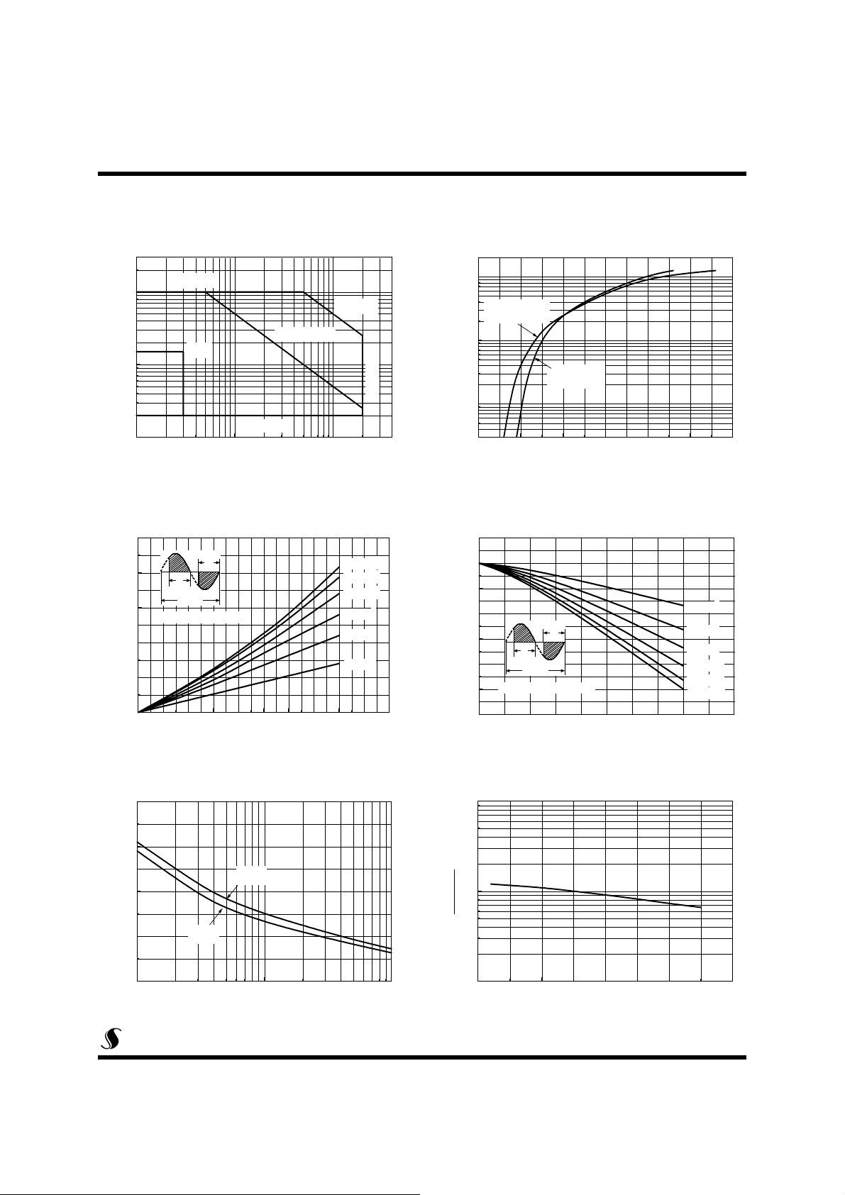
Fig 1. Gate Characteristics Fig 2. On-State Voltage
2
VGM (10V)
1
10
PGM (5W)
P
(0.5W)
0
10
25 ℃
G(AV)
Gate Voltage [V]
-1
10
1
10
2
10
VGD (0.2V)
3
10
(2A)
GM
I
Gate C urrent [mA]
10
TJ = 125 oC
1
10
On-State Current [A]
0
10
0.5 1.0 1.5 2.0 2.5 3.0 3.5
BT139-600
TJ = 25 oC
On-S ta te Voltage [V]
Fig 3. On State Current vs.
Maximum Power Dissipation
25
θ
π
π
20
15
10
Power Dissipation [W]
5
0
θ
θ
: Conduction Angle
02468101214161820
2
360°
θ = 180
θ = 150
θ = 120
θ = 90
θ = 60
θ = 30
RMS O n -State C u rrent [A]
Fig 5. Surge On-State Current Rating
( Non-Repetitive )
200
150
100
50
Surge On-State Current [ A]
50Hz
60Hz
Fig 4. On State Current vs.
Allowable Case Temperature
130
o
o
o
o
o
o
C]
o
125
120
115
θ
π
π
110
2
θ
105
Allowable Case Temperatur e [
100
95
048121620
360°
θ
: Conduction Angle
θ = 30
θ = 60
θ = 90
θ = 120
θ = 150
θ = 180
o
o
o
o
o
o
RM S On-Sta te Current [ A ]
Fig 6. Gate Trigger Voltage vs.
Junction Temperature
10
C)
C)
o
o
1
(t
(25
GT
GT
V
V
0
0
10
1
10
2
10
Time (cycles)
0.1
-50 0 50 100 150
Junction Temperature [ oC]
3/5
BT139-600
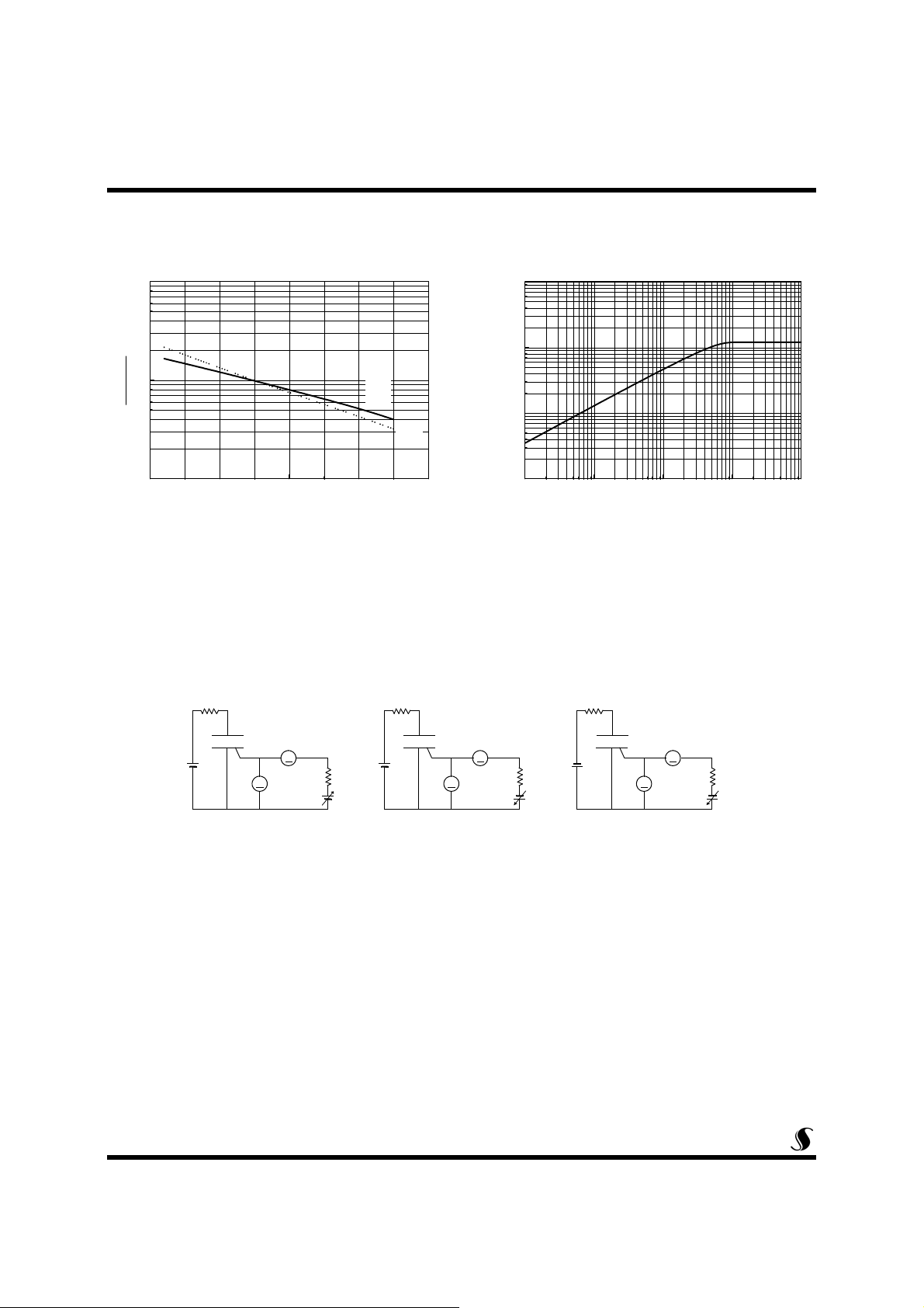
Fig 7. Gate Trigger Current vs.
Junction Temperature
10
C)
C)
o
o
1
(t
(25
GT
I
GT
I
0.1
-50 0 50 100 150
Junction Temperature [ oC]
Fig 9. Gate Trigger Characteristics Test Circuit
Fig 8. Transient Thermal Impedance
1
10
C/W]
o
0
10
+
I
GT1
_
I
GT1
-1
_
I
GT3
10
-2
10
Transient Thermal Impedance [
-3
10
-2
10
-1
10
Time (sec)
0
10
1
10
4/5
10Ω
6V
▼
▲
10Ω
▼
●
A
R
V
●
G
6V
▲
●
A
V
●
R
10Ω
▼
▲
●
G
6V
A
V
●
Test Procedure Ⅰ Test Procedure Ⅱ Test Procedure Ⅲ
R
G
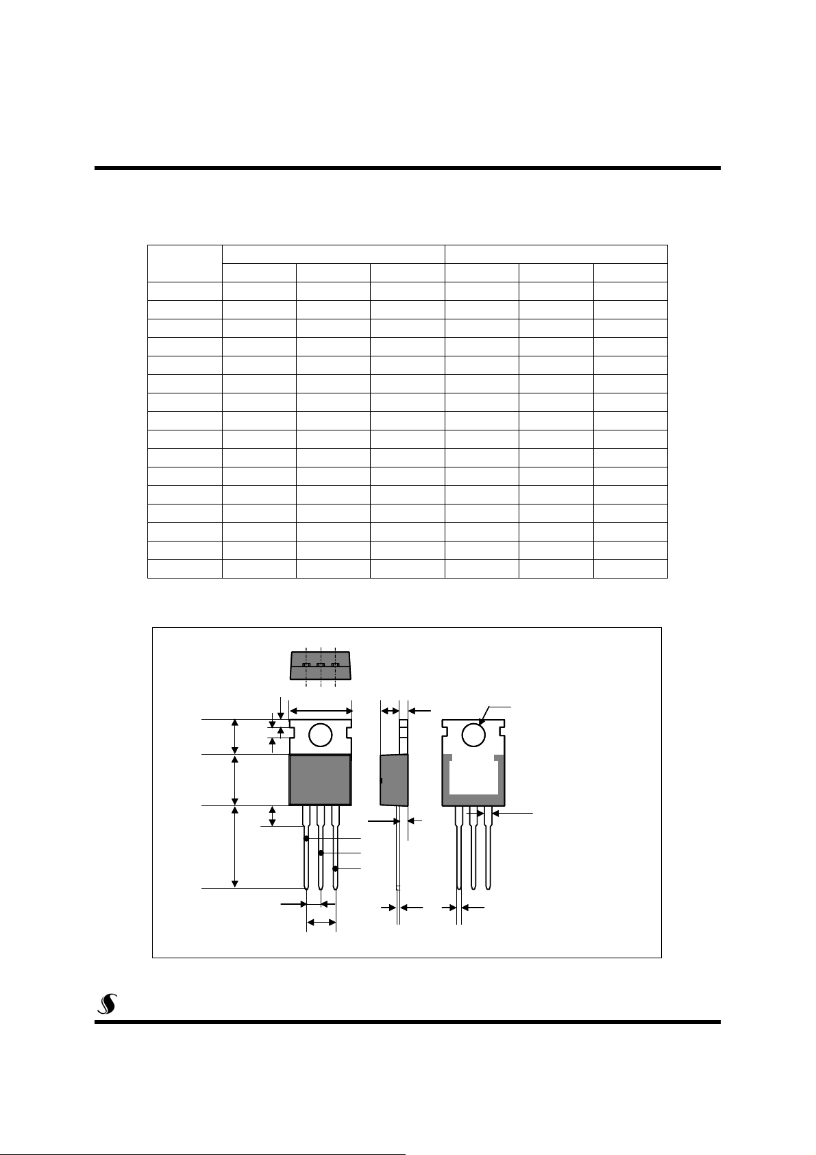
TO-220 Package Dimension
BT139-600
Dim.
Min. Typ. Max. Min. Typ. Max.
mm Inch
A 9.7 10.1 0.382 0.398
B 6.3 6.7 0.248 0.264
C 9.0 9.47 0.354 0.373
D 12.8 13.3 0.504 0.524
E 1.2 1.4 0.047 0.055
F 1.7 0.067
G 2.5 0.098
H 3.0 3.4 0.118 0.134
I 1.25 1.4 0.049 0.055
J 2.4 2.7 0.094 0.106
K 5.0 5.15 0.197 0.203
L 2.2 2.6 0.087 0.102
M 1.25 1.55 0.049 0.061
N 0.45 0.6 0.018 0.024
O 0.6 1.0 0.024 0.039
φ
3.6 0.142
I
E
B
F
C
G
D
A
H
L
1
2
3
φ
M
1. T1
2. T2
3. Gate
J
K
N
O
5/5
 Loading...