


SUMMIT SMS2902P, SMS2902P2.7, SMS2902PA, SMS2902PB, SMS2902S Datasheet
...SUMMIT
MICROELECTRONICS, Inc. SMS2902/SMS2904/SMS2916
Voltage Supervisory Circuit With Watchdog Timer
FEATURES
•Precision Voltage Monitor
–VCC Supply Monitor
-Complementary reset outputs for complex microcontroller systems
-Integrated memory write lockout function
-No external components required
•Watchdog Timer
–1600 ms, internal
•Two Wire Serial Interface (I2C™)
•Extended Programmable Functions available on SMS24
•High Reliability
–Endurance: 100,000 erase/write cycles
–Data retention: 100 years
•8-Pin PDIP or SOIC Packages
OVERVIEW
The SMS29xx is a power supervisory circuit that monitors VCC and will generate complementary reset outputs. The reset pins also act as I/Os and may be used for signal conditioning. The SMS29xx also has an on-board watchdog timer.
The SMS29xx integrates a nonvolatile serial memory. It features the industry standard I2C serial interface allowing quick implementation in an end-users’ system.
BLOCK DIAGRAM
VCC 8
SCL |
6 |
|
NONVOLATILE |
SDA |
5 |
|
MEMORY |
|
ARRAY |
||
|
|
|
|
|
|
|
WRITE |
|
|
|
CONTROL |
|
|
|
PROGRAMMABLE |
|
|
|
RESET PULSE |
|
|
|
GENERATOR |
|
+ |
VTRIP |
RESET |
|
– |
|
CONTROL |
|
1.26V |
|
WATCHDOG |
WDI# |
1 |
|
|
|
TIMER |
||
|
|
|
4
GND |
2028 T BD 2.0 |
2 RESET#
7 RESET
SUMMIT MICROELECTRONICS, Inc. • 300 Orchard City Drive, Suite 131 |
• Campbell, CA 95008 • Telephone 408-378- 6461 • Fax 408-378-6586 • www.summitmicro.com |
© SUMMIT MICROELECTRONICS, Inc. 2000 |
Characteristics subject to change without notice |
2028 5.0 4/18/00 |
1 |

SMS2902/SMS2904/SMS2916
PIN CONFIGURATIONS |
|
|
|
PIN NAMES |
|
|
|||||
|
|
|
|
|
|
|
|
|
|
|
|
|
|
|
|
8-Pin PDIP |
|
|
Symbol |
Pin |
Description |
||
|
|
|
|
|
|
|
|
|
|||
|
|
|
|
WDI# |
1 |
Watchdog Input /a high to |
|||||
|
|
|
or 8-Pin SOIC |
|
|
||||||
|
|
|
|
|
|
|
|
|
|
|
low transition will clear the |
|
|
|
|
|
|
|
|
|
|
|
watchdog timer |
|
|
|
|
|
|
|
|
|
|
|
|
WDI# |
|
|
1 |
8 |
|
VCC |
|
RESET# |
2 |
Active Low RESET Input/Output |
|
|
|
|
|
||||||||
|
|
|
|
||||||||
RESET# |
|
|
|
2 |
7 |
|
RESET |
|
NC |
3 |
No Connect, tie to ground |
|
|
|
|
|
|||||||
|
|
|
|
|
|||||||
NC |
|
|
3 |
6 |
|
SCL |
|
||||
|
|
|
|
|
|
or leave open |
|||||
|
|
|
|
|
|
||||||
GND |
|
|
4 |
5 |
|
SDA |
|
|
|
||
|
|
|
|
|
|
|
|||||
|
GND |
4 |
Analog and Digital Ground |
||||||||
|
|
|
|
||||||||
|
|
|
|
|
|
|
|
|
|||
|
|
|
|
|
|
|
|
|
|||
|
|
|
|
|
|
|
|
|
|
|
|
|
|
|
|
|
2028 T PCon 2.0 |
|
SDA |
5 |
Serial Memory Input/ |
||
|
|
|
|
|
|
|
|
Output data line |
|||
|
|
|
|
|
|
|
|
|
|
|
|
|
|
|
|
|
|
|
|
|
|
|
|
|
|
|
|
|
|
|
|
|
SCL |
6 |
Serial Memory clock input |
|
|
|
|
|
|
|
|
|
|
|
|
|
|
|
|
|
|
|
|
|
RESET |
7 |
Active High RESET Input/ |
|
|
|
|
|
|
|
|
|
|
|
Output |
|
|
|
|
|
|
|
|
|
|
|
|
|
|
|
|
|
|
|
|
|
VCC |
8 |
Supply Voltage |
|
|
|
|
|
|
|
|
|
|
|
|
2028 PGM T1.1
CAPACITANCE |
|
|
|
|
TA = 25°C, f = 100KHz |
|
|
|
|
Symbol |
Parameter |
|
Max |
Units |
CIN |
Input Capacitance |
|
5 |
pF |
LOUT |
Output Capacitance |
|
8 |
pF |
|
|
|
|
2028 PGM T2..0 |
tR |
tH IGH |
tLOW |
tSU:STO |
|
|
tF |
|
|
|
SCL |
|
|
|
|
tSU:SDA |
tHD:SDA |
|
|
|
|
tHD:DAT |
|
tSU:DAT |
tBUF |
|
|
|
|
|
SDA In |
|
|
|
|
|
tAA |
tDH |
|
|
|
|
|
|
|
SDA Out |
|
|
|
|
|
|
|
|
2028 ILL5.0 |
|
FIGURE 1. SERIAL BUS TIMING DIAGRAM |
|
||
2028 5.0 4/18/00 |
2 |
|
|
|
|
|
|
|
|

|
|
|
|
SMS2902/SMS2904/SMS2916 |
|
|
|
|
|
ABSOLUTE MAXIMUM RATINGS |
|
|||
Temperature Under Bias ............................................................................................................................... |
-40°C to +85°C |
|||
Storage Temperature ..................................................................................................................................... |
-65°C to +125°C |
|||
Soldering Temperature (less than 10 seconds) ................................................................................................................... |
300°C |
|||
Supply Voltage ............................................................................................................................................................. |
0 to 6.5V |
|||
Voltage on Any Pin ....................................................................................................................................... |
-0.3V to VCC+0.3V |
|||
ESD Voltage (JEDEC method) .......................................................................................................................................... |
2,000V |
|||
NOTE: These are STRESS ratings only. Appropriate conditions for operating these devices are given elsewhere in this specification. Stresses beyond those listed here may permanently damage the part. Prolonged exposure to maximum ratings may affect device reliability.
RECOMMENDED OPERATING CONDITIONS
Temperature |
Min |
Max |
Commercial |
0°C |
+70°C |
Industrial |
-40°C |
+85°C |
2028 PGM T3.0
DC ELECTRICAL CHARACTERISTICS (over recommended operating conditions unless otherwise specified)
Symbol |
Parameter |
Conditions |
|
Min |
Max |
Units |
|
|
|
|
|
|
|
|
|
|
|
SCL = CMOS Levels @ 100KHz |
VCC =5.5V |
|
3 |
mA |
|
ICC |
Supply Current (CMOS) |
SDA = Open |
|
|
|
|
|
|
|
|
|
|
|||
|
|
All other inputs = GND or VCC |
VCC =3.3V |
|
2 |
mA |
|
|
|
|
|
|
|
|
|
ISB |
Standby Current (CMOS) |
SCL = SDA = VCC |
VCC =5.5V |
|
50 |
µA |
|
|
|
All other inputs = GND |
VCC =3.3V |
|
25 |
µA |
|
ILI |
Input Leakage |
VIN = 0 To VCC |
|
|
10 |
µA |
|
|
|
|
|
|
|
|
|
ILO |
Output Leakage |
VOUT = 0 To VCC |
|
|
10 |
µA |
|
|
|
|
|
|
|
|
|
VIL |
Input Low Voltage |
S0, S1, S2, SCL, SDA, RESET# |
|
|
0.3xVCC |
V |
|
|
|
|
|
|
|
|
|
VIH |
Input High Voltage |
S0, S1, S2, SCL, SDA, RESET |
|
0.7xVCC |
|
V |
|
|
|
|
|
|
|
|
|
VOL |
Output Low Voltage |
IOL = 3mA SDA |
|
|
0.4 |
V |
|
|
|
|
|
|
|
|
|
2028 PGM T4.0
AC ELECTRICAL CHARACTERISTICS |
|
|
|
|
|
|
|
(over recommended operating conditions unless otherwise specified) |
2.7V to 4.5V |
4.5V to 5.5V |
|
||||
|
|
|
|
|
|
|
|
Symbol |
Parameter |
Conditions |
Min |
Max |
Min |
Max |
Units |
|
|
|
|
|
|
|
|
fSCL |
SCL Clock Frequency |
|
0 |
100 |
|
400 |
KHz |
|
|
|
|
|
|
|
|
tLOW |
Clock Low Period |
|
4.7 |
|
1.3 |
|
µs |
|
|
|
|
|
|
|
|
tHIGH |
Clock High Period |
|
4.0 |
|
0.6 |
|
µs |
|
|
|
|
|
|
|
|
tBUF |
Bus Free Time |
Before New Transmission |
4.7 |
|
1.3 |
|
µs |
|
|
|
|
|
|
|
|
tSU:STA |
Start Condition Setup Time |
|
4.7 |
|
0.6 |
|
µs |
|
|
|
|
|
|
|
|
tHD:STA |
Start Condition Hold Time |
|
4.0 |
|
0.6 |
|
µs |
|
|
|
|
|
|
|
|
tSU:STO |
Stop Condition Setup Time |
|
4.7 |
|
0.6 |
|
µs |
|
|
|
|
|
|
|
|
tAA |
Clock to Output |
SCL Low to SDA Data Out Valid |
0.3 |
3.5 |
0.2 |
0.9 |
µs |
|
|
|
|
|
|
|
|
tDH |
Data Out Hold Time |
SCL Low to SDA Data Out Change |
0.3 |
|
0.2 |
|
µs |
|
|
|
|
|
|
|
|
tR |
SCL and SDA Rise Time |
|
|
1000 |
|
300 |
ns |
|
|
|
|
|
|
|
|
tF |
SCL and SDA Fall Time |
|
|
300 |
|
300 |
ns |
|
|
|
|
|
|
|
|
tSU:DAT |
Data In Setup Time |
|
250 |
|
100 |
|
ns |
|
|
|
|
|
|
|
|
tHD:DAT |
Data In Hold Time |
|
0 |
|
0 |
|
ns |
|
|
|
|
|
|
|
|
TI |
Noise Spike Width |
Noise Suppression Time Constant |
|
100 |
|
100 |
ns |
|
@ SCL, SDA Inputs |
|
|
|
|
|
|
|
|
|
|
|
|
|
|
tWR |
Write Cycle Time |
|
|
10 |
|
10 |
ms |
|
|
|
|
|
|
|
|
|
|
|
|
|
|
2028 PGM T5.0 |
|
|
|
|
|
|
|
|
|
|
|
3 |
|
|
|
2028 5.0 4/18/00 |
|
|
|
|
|
|
|
|
|
|
|
SMS2902/SMS2904/SMS2916 |
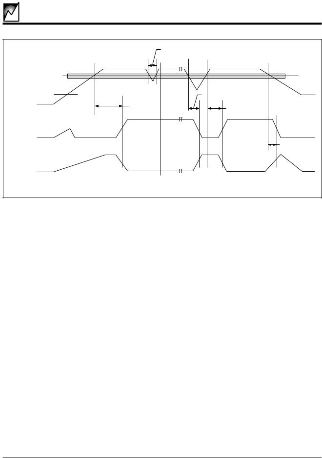
|
|
tGLITCH |
VTRIP |
|
|
VRVALID |
|
tRPD |
VCC |
tPURST |
tPURST |
|
|
|
RESET# |
|
tRPD |
|
|
|
RESET |
|
|
|
|
2028 T fig02 2.0 |
|
FIGURE 2. RESET OUTPUT TIMING |
|
RESET CIRCUIT AC and DC ELECTRICAL CHARACTERISTICS
TA=-40°C to +85°C
Symbol |
Parameter |
Part no. |
Min. |
Typ. |
Max. |
Unit |
|
|
Suffix |
|
|
|
|
VTRIP |
Reset Trip Point |
A (or) Blank |
4.250 |
4.375 |
4.5 |
V |
|
|
B |
4.50 |
4.625 |
4.75 |
V |
|
|
2.7 |
2.55 |
2.65 |
2.75 |
V |
tPURST |
Reset Timeout |
|
|
200 |
|
ms |
tRPD |
VTRIP to RESET Output Delay |
|
|
|
5 |
µs |
|
|
|
|
|
|
|
VRVALID |
RESET Output Valid to VCC min. Guarantee |
|
1 |
|
|
V |
|
|
|
|
|
|
|
tGLITCH |
Glitch Reject Pulse Width note 1 |
|
|
30 |
|
ns |
VOLRS |
RESET Output Low Voltage IOL = 1mA |
|
|
|
0.4 |
V |
|
|
|
|
|
|
|
VOHRS |
RESET High Voltage Output IOH = 800µA |
|
VCC-.75 |
|
|
V |
|
|
|
|
|
|
|
VULH |
VSENSE Under-voltage threshold low to high |
|
1.20 |
1.25 |
1.30 |
V |
VUHL |
VSENSE Under-voltage threshold high to low |
|
1.20 |
1.25 |
1.30 |
V |
VOLH |
VSENSE Over-voltage threshold low to high |
|
1.20 |
1.25 |
1.30 |
V |
|
|
|
|
|
|
|
VOHL |
VSENSE Over-voltage threshold high to low |
|
1.20 |
1.25 |
1.30 |
V |
|
|
|
|
|
|
|
tVD1 |
Delay to VLOW Active |
|
|
|
5 |
µs |
tVD2 |
Delay to VLOW Released |
|
|
|
5 |
µs |
tWDTO |
Watchdog timeout Period |
|
|
1600 |
|
ms |
2028 5.0 4/18/00
4
|
|
|
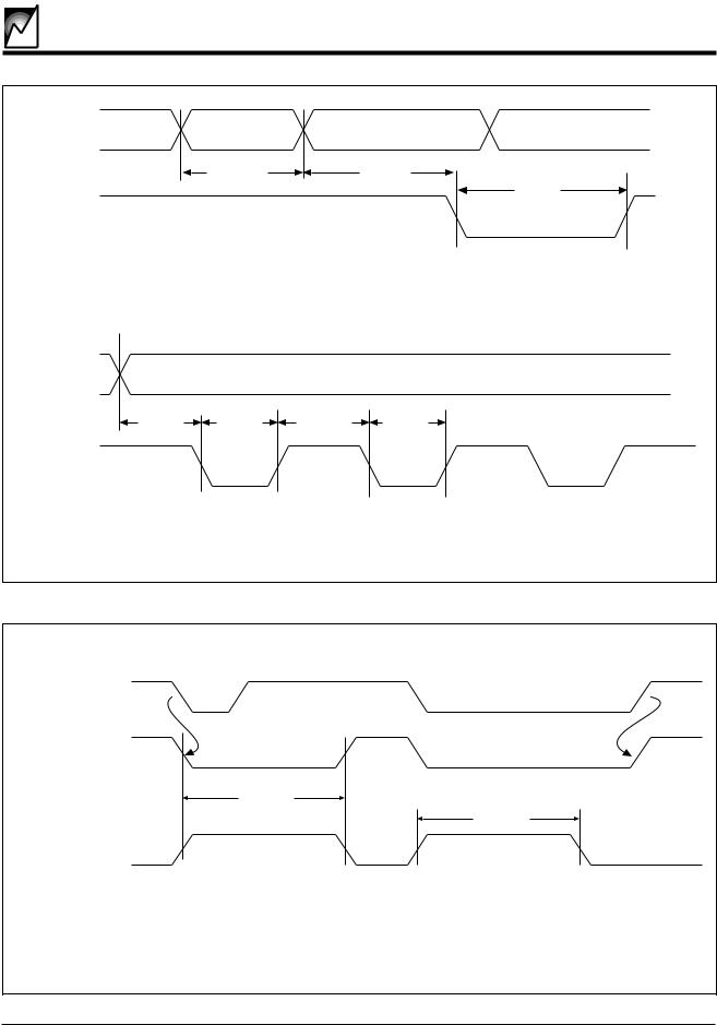
SMS2902/SMS2904/SMS2916 |
WDI# |
|
|
|
|
< tWDTO |
|
tWDTO |
|
|
|
tPURST |
RESET# |
|
|
|
WDI# |
|
|
|
tWDTO |
tPURST |
tWDTO |
tPURST |
RESET# |
|
|
|
|
|
|
2028 T fig03 2.0 |
|
FIGURE 3. WATCHDOG TIMER TIMING DIAGRAM |
||
RESET# (in) |
RESET# (out) |
tPURST |
tPURST |
RESET (out) |
2028 T fig04 2.0 |
FIGURE 4. RESET AS AN INPUT FUNCTION |
2028 5.0 4/18/00 |
5 |
 Loading...