


SUMMIT SMS24S1R1R1R0R0, SMS24S2R1R1R0R0, SMS24S3R1R1R0R0, SMS24S4R1R1R0R0, SMS24S5R1R1R0R0 Datasheet
...SUMMIT |
SMS24 |
MICROELECTRONICS, Inc. |
|
Highly Programmble Voltage Supervisory Circuit |
|
FEATURES
lUser Programmable Device Configuration
lGuaranteed Reset Valid to VCC = 1V
lImmune to Short Negative VCC Transients
lSix Unique Pin Configurations
lUser Programmable Feature Options: w Reset Threshold Voltages
w Reset Pulse Widths
w Programmable Watchdog Timeouts
w Programmable Overor Under-Voltage Sensing
lHigh Reliability
wEndurance: 100,000 erase/write cycles
wData retention: 100 years
INTRODUCTION
The SMS24 is a configurable and in-system programmable second generation 8 pin supervisory circuit. This single device is adaptable to provide the optimum functionality for a given system or sub-system. User programmable functions available — reset pulse width, watchdog delays, and voltage monitor thresholds — eliminate external components and allow standardization to enhance system reliability. Additionally, 4K bits of general purpose EEPROM is available on all configurations. The SMS24 is available in six pin configurations, and is compatible with all Summit programmable devices and other I2C components.
Programming of configuration, control and calibration values by the user can be simplified with the interface adapter and Windows GUI software obtainable from Summit Microelectronics.
DEVICE TYPES
|
|
|
|
|
|
|
|
|
|
|
|
|
|
|
|
Function |
|
|
|
|
|
|
|
|
|
|
|
|||
Device |
|
|
|
|
|
|
|
|
|
|
|
|
|
|
|
|
|
|
|
|
|
|
|
|
|
|
||||
|
|
|
|
|
|
|
|
|
Software |
|
|
|
Write |
|
2nd |
|
Manual |
|
|
NV |
||||||||||
Code |
|
Reset# |
Reset |
Watchdog |
WDI Pin |
Protect |
|
Voltage |
|
Reset |
|
|
||||||||||||||||||
|
|
|
|
|
|
|
|
|
|
WDI |
|
|
|
|
Pin |
|
Monitor |
|
Input |
|
|
Memory |
||||||||
|
|
|
|
|
|
|
|
|
|
|
|
|
|
|
|
|
|
|
|
|
|
|
|
|||||||
|
|
|
|
|
|
|
|
|
|
|
|
|
|
|
|
|
|
|
|
|
|
|
|
|
|
|||||
001 |
|
|
|
|
|
|
|
|
|
|
|
|
|
|
|
|
|
|
|
|
|
|
|
|
|
|||||
|
|
|
|
|
|
|
|
|
|
|
|
|
|
|
|
|
|
|
|
|
|
|
|
|
|
|
||||
010 |
|
|
|
|
|
|
|
|
|
|
|
|
|
|
|
|
|
|
|
|
|
|
|
|
|
|
||||
|
|
|
|
|
|
|
|
|
|
|
|
|
|
|
|
|
|
|
|
|
|
|
|
|
|
|
|
|
|
|
011 |
|
|
|
|
|
|
|
|
|
|
|
|
|
|
|
|
|
|
|
|
|
|
|
|
|
|
|
|
|
|
|
|
|
|
|
|
|
|
|
|
|
|
|
|
|
|
|
|
|
|
|
|
|
|
|
|
|
||||
100 |
|
|
|
|
|
|
|
|
|
|
|
|
|
|
|
|
|
|
|
|
|
|
|
|
|
|
||||
|
|
|
|
|
|
|
|
|
|
|
|
|
|
|
|
|
|
|
|
|
|
|||||||||
101 |
|
|
|
|
|
|
|
|
|
|
|
|
|
|
|
|
|
|
|
|
|
|||||||||
|
|
|
|
|
|
|
|
|
|
|
|
|
|
|
|
|
|
|
|
|
|
|
|
|
|
|
||||
110 |
|
|
|
|
|
|
|
|
|
|
|
|
|
|
|
|
|
|
|
|
|
|
|
|
|
|
||||
|
|
|
|
|
|
|
|
|
|
|
|
|
|
|
|
|
|
|
|
|
|
|
|
|
|
|
|
|
|
|
|
|
|
|
|
|
|
|
|
|
|
|
|
|
|
|
|
|
|
|
|
|
|
|
|
|
|
|
|
|
2048 DTTable 2.1 |
NC |
|
|
|
|
|
VCC |
|
|
NC |
|
|
|
|
|
VCC |
|
WDI |
|
|
|
|
|
|
VCC |
||||||
RESET# |
|
|
Device |
|
RESET |
RESET# |
|
|
Device |
|
WP |
RESET# |
|
|
Device |
|
|
RESET |
||||||||||||
|
|
Code |
|
|
|
Code |
|
|
|
|
Code |
|
|
|||||||||||||||||
|
|
|
|
|
|
|
|
|
||||||||||||||||||||||
NC |
|
|
|
SCL |
|
|
NC |
|
|
|
|
SCL |
|
NC |
|
|
|
|
|
|
SCL |
|||||||||
|
|
001 |
|
|
|
|
|
|
010 |
|
|
|
|
|
011 |
|
|
|||||||||||||
GND |
|
|
|
SDA |
|
GND |
|
|
|
|
|
SDA |
|
GND |
|
|
|
|
|
|
SDA |
|||||||||
|
|
|
|
|
|
|
|
|
|
|
|
|
|
|
|
|
|
|
|
|
|
|
|
|
|
|
|
|
|
|
RESET#2 |
|
Device |
|
|
VCC |
VLOW# |
|
|
Device |
|
VCC |
VLOW# |
|
Device |
|
VCC |
||||
|
|
|
|
|
|
|
|
|||||||||||||
RESET#1 |
|
|
|
MR# |
RESET# |
|
|
|
RESET |
RESET# |
|
|
WDI |
|||||||
|
Code |
|
|
|
|
Code |
|
|
Code |
|
||||||||||
|
|
|
|
|
|
|
|
|||||||||||||
VSENSE |
|
|
|
SCL |
VSENSE |
|
|
|
|
SCL |
VSENSE |
|
|
SCL |
||||||
|
100 |
|
|
|
|
|
101 |
|
|
110 |
|
|||||||||
|
|
|
|
|
|
|
|
|
||||||||||||
GND |
|
|
|
|
SDA |
GND |
|
|
|
|
|
SDA |
GND |
|
|
|
SDA |
|||
|
|
|
|
|
|
|
|
|
|
|
|
|
|
|
|
|
|
|
|
|
|
|
|
|
|
|
|
|
|
|
|
|
|
|
|
|
|
|
2046 DT 1.0 |
||
©SUMMIT MICROELECTRONICS, Inc., 2001 |
• 300 Orchard City Dr., Suite 131 |
|
• Campbell, CA 95008 • Phone 408-378-6461 • FAX 408- 378-6586 • www.summitmicro.com |
|||||||||||||||||
|
|
|
|
|
|
|
|
|
|
|
|
|
|
|
|
|
|
|
|
|
Characteristics subject to change without notice |
|
|
|
|
|
2048 2.4. 3/1/01 |
|
|
|
|
|
|
1 |
|||||||

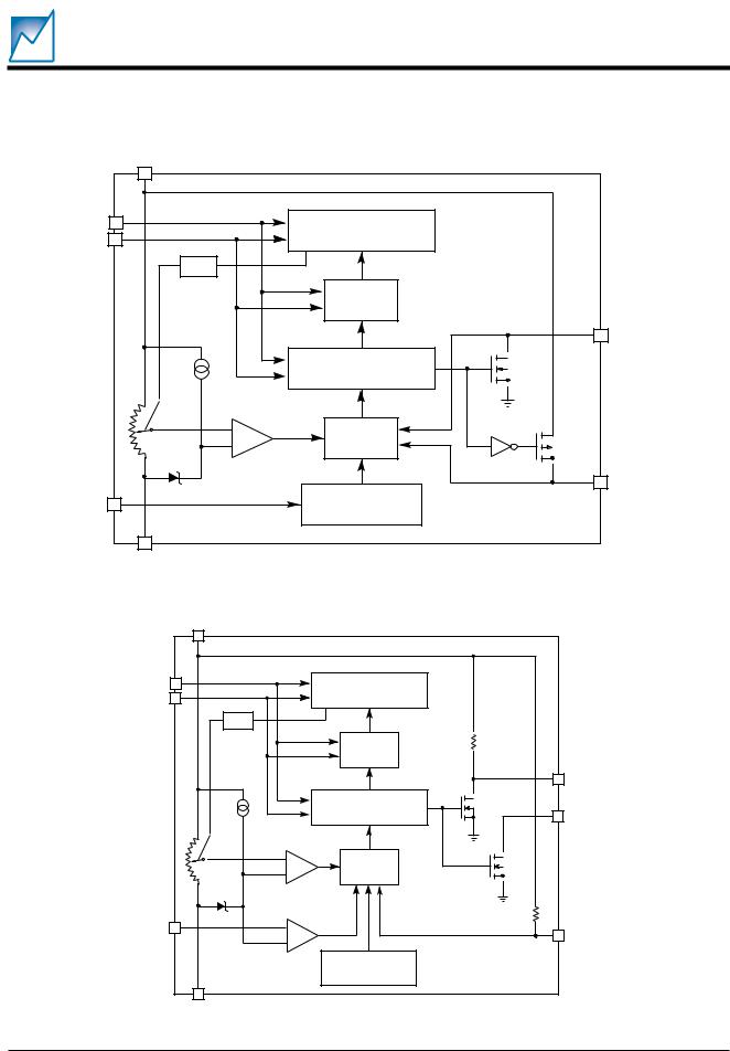
SMS24
FUNCTIONAL BLOCK DIAGRAMS
|
VCC |
|
|
|
8 |
|
|
SCL |
6 |
NONVOLATILE |
|
SDA |
5 |
MEMORY |
|
ARRAY |
|||
|
|
||
|
|
WRITE |
|
|
|
CONTROL |
|
|
|
PROGRAMMABLE |
|
|
|
RESET PULSE |
|
|
|
GENERATOR |
|
|
VTRIP |
|
|
|
+ |
RESET |
|
|
|
||
|
– |
CONTROL |
|
|
1.25V |
PROGRAMMABLE |
|
|
|
WATCHDOG |
|
|
|
TIMER |
|
|
4 |
|
|
|
GND |
2046 BD001 2.1 |
2 RESET#
7 RESET
|
|
Block Diagram Device Code 001 |
|
|
|
VCC |
|
|
|
|
8 |
|
|
|
SCL |
6 |
NONVOLATILE |
|
|
SDA |
5 |
MEMORY |
|
|
ARRAY |
|
|
||
|
|
|
|
|
|
|
WRITE |
7 |
WP |
|
|
CONTROL |
|
|
|
|
|
2 |
RESET# |
|
|
PROGRAMMABLE |
|
|
|
|
RESET PULSE |
|
|
|
|
GENERATOR |
|
|
|
VTRIP |
|
|
|
|
+ |
RESET |
|
|
|
|
|
|
|
|
– |
CONTROL |
|
|
|
1.25V |
PROGRAMMABLE |
|
|
|
|
WATCHDOG |
|
|
|
|
TIMER |
|
|
|
4 |
|
|
|
|
GND |
2046 BD010 2.1 |
|
|
Block Diagram Device Code 010
2 |
2048 2.4. 3/1/01 |
SUMMIT MICROELECTRONICS, Inc. |
|
|
SMS24
|
VCC |
|
|
|
8 |
|
|
SCL |
6 |
NONVOLATILE |
|
SDA |
5 |
MEMORY |
|
ARRAY |
|||
|
|
||
|
|
WRITE |
|
|
|
CONTROL |
|
|
|
PROGRAMMABLE |
|
|
|
RESET PULSE |
|
|
|
GENERATOR |
|
|
VTRIP |
|
|
|
+ |
RESET |
|
|
|
||
|
– |
CONTROL |
|
|
1.25V |
PROGRAMMABLE |
|
WDI |
1 |
||
WATCHDOG |
|||
|
|
TIMER |
|
|
4 |
|
|
|
GND |
2046 BD011 1.0 |
2 RESET#
7 RESET
|
|
Block Diagram Device Code 011 |
|
|
|
|
VCC |
|
|
|
|
|
8 |
|
|
|
|
SCL |
6 |
|
NONVOLATILE |
|
|
SDA |
5 |
|
MEMORY |
|
|
|
ARRAY |
|
|
||
|
|
|
|
|
|
|
|
|
WRITE |
|
|
|
|
|
CONTROL |
|
|
|
|
|
|
2 |
RESET#1 |
|
|
|
PROGRAMMABLE |
|
|
|
|
|
RESET PULSE |
1 |
RESET#2 |
|
|
|
GENERATOR |
||
|
|
VTRIP |
|
|
|
|
|
+ |
RESET |
|
|
|
|
|
|
|
|
|
|
– |
CONTROL |
|
|
|
|
1.25V |
|
|
|
VSENSE |
3 |
+ |
|
7 |
MR# |
|
|
– |
|
||
|
|
|
|
|
|
|
|
|
PROGRAMMABLE |
|
|
|
|
|
WATCHDOG |
|
|
|
|
|
TIMER |
|
|
|
4 |
|
|
|
|
|
GND |
|
2046 BD100 1.1 |
|
|
Block Diagram Device Code 100
SUMMIT MICROELECTRONICS, Inc. |
2048 2.4. 3/1/01 |
3

SMS24
|
VCC |
|
|
|
8 |
|
|
SCL |
6 |
|
NONVOLATILE |
SDA |
5 |
|
MEMORY |
|
ARRAY |
||
|
|
|
|
|
|
|
WRITE |
|
|
|
CONTROL |
|
|
|
PROGRAMMABLE |
|
|
|
RESET PULSE |
|
|
|
GENERATOR |
|
|
VTRIP |
|
|
|
+ |
RESET |
|
|
|
|
|
|
– |
CONTROL |
|
|
1.25V |
PROGRAMMABLE |
|
|
WATCHDOG |
|
|
|
|
|
|
|
|
TIMER |
VSENSE |
3 |
+ |
UV |
|
|||
|
|
– |
OV |
|
|
|
|
|
4 |
|
|
|
GND |
|
2046 BD101 1.0 |
2 RESET#
7 RESET
1 VLOW#
|
|
Block Diagram Device Code 101 |
|
|
VCC |
|
|
|
8 |
|
|
SCL |
6 |
|
NONVOLATILE |
SDA |
5 |
|
MEMORY |
|
ARRAY |
||
|
|
|
|
|
|
|
WRITE |
|
|
|
CONTROL |
|
|
|
PROGRAMMABLE |
|
|
|
RESET PULSE |
|
|
|
GENERATOR |
|
|
VTRIP |
|
|
|
+ |
RESET |
|
|
|
|
|
|
– |
CONTROL |
|
|
1.25V |
PROGRAMMABLE |
|
|
WATCHDOG |
|
|
|
|
|
|
|
|
TIMER |
VSENSE |
3 |
+ |
UV |
|
|||
|
|
– |
OV |
|
|
|
|
|
4 |
|
|
|
GND |
|
2046 BD110 1.0 |
Block Diagram Device Code 110
2 RESET#
7 WDI
1 VLOW#
4 |
2048 2.4. 3/1/01 |
SUMMIT MICROELECTRONICS, Inc. |
|
|

SMS24
ABSOLUTE MAXIMUM RATINGS*
Temperature Under Bias ....................... |
-55°C to 125°C |
Storage Temperature ............................ |
-65°C to 150°C |
Lead Solder Temperature (10 secs) ................... |
300 °C |
Terminal Voltage with Respect to GND: |
|
VCC ................................. |
-0.3V to 6.0V |
All Others ........................ |
-0.3V to 6.0V |
*COMMENT
Stresses listed under Absolute Maximum Ratings may cause permanent damage to the device. These are stress ratings only, and functional operation of the device at these or any other conditions outside those listed in the operational sections of this specification is not implied. Exposure to any absolute maximum rating for extended periods may affect device performance and reliability.
DC OPERATING CHARACTERISTICS
(Over Recommended Operating Conditions; Voltages are relative to GND)
Symbol |
Parameter |
|
Conditions |
|
Min. |
Typ. |
Max. |
Units |
|||
|
|
|
|
|
|
|
|
|
|
|
|
VCC |
Operating supply |
Valid RESET# output |
|
1 |
|
5.5 |
V |
||||
|
|
|
|
|
|
|
|
|
|
||
voltage |
Memory operaton |
|
|
2.7 |
|
5.5 |
V |
||||
|
|
|
|
||||||||
|
|
|
|
|
|||||||
|
|
|
|
|
|
|
|
|
|
|
|
|
|
3.6V < VCC < 5.5V |
|
|
|
50 |
µA |
||||
ICC |
Supply current |
2.7V < VCC < 3.6V |
|
|
|
20 |
µA |
||||
|
|
Memory access |
|
|
|
|
3 |
µA |
|||
|
|
|
|
|
|
|
|
|
|
|
|
|
|
RR4 |
RR3 |
RR2 |
RR1 |
RR0 |
|
|
|
|
|
|
|
|
|
|
|
|
|
|
|
|
|
|
|
0 |
0 |
0 |
|
0 |
1 |
2.075 |
2.15 |
2.25 |
V |
|
|
|
|
|
|
|
|
|
|
|
|
VPRST |
Programmable reset threshold |
0 |
0 |
0 |
|
1 |
0 |
2.55 |
2.65 |
2.7 |
V |
|
|
|
|
|
|
|
|
|
|
||
0 |
0 |
1 |
|
0 |
0 |
2.8 |
2.9 |
3.0 |
V |
||
|
|
|
|||||||||
|
|
|
|
|
|
|
|
|
|
|
|
|
|
0 |
1 |
0 |
|
0 |
0 |
4.25 |
4.375 |
4.5 |
V |
|
|
|
|
|
|
|
|
|
|
|
|
|
|
1 |
0 |
0 |
|
0 |
0 |
4.5 |
4.625 |
4.75 |
V |
|
|
|
|
|
|
|
|
|
|
|
|
VT |
VSENSE input threshold |
|
|
|
|
|
|
1.23 |
1.25 |
1.27 |
V |
|
RESET#1, RESET#2, VLOW#: |
ISINK = 1.2mA, VCC = VPRST |
|
|
0.3 |
V |
|||||
VOL |
min. |
|
|
|
|
|
|
|
|||
|
|
|
|
|
|
|
|
|
|||
output voltage |
|
|
|
|
|
|
|
|
|
|
|
ISINK = 200mA, VCC = 1.2V |
|
|
0.3 |
V |
|||||||
|
|
|
|||||||||
|
|
|
|
||||||||
IMR |
MR# pullup current |
|
|
|
|
|
|
|
100 |
|
µA |
VlL |
Noise rejection on VCC |
|
|
|
|
|
|
|
|
0.3 × VCC |
V |
VIH |
Delay threshold crossing to |
|
|
|
|
|
|
0.7 × VCC |
|
|
V |
RESET out |
|
|
|
|
|
|
|
|
|||
|
|
|
|
|
|
|
|
|
|
|
|
|
|
|
|
|
|
|
|
|
|
|
|
RECOMMENDED OPERATING CONDITIONS
Temperature |
–40ºC to 85ºC. |
Voltage |
2.7V to 5.5V |
2046 DCElect Table 2.0
ENDURANCE AND DATA RETENTION
The SMS24 is designed for applications requiring 100,000 erase/write cycles and unlimited read cycles. It provides 100 years of secure data retention, with or without power applied, after the execution of 100,000 erase/write cycles.
SUMMIT MICROELECTRONICS, Inc. |
2048 2.4. 3/1/01 |
5

SMS24
PIN DESCRIPTIONS
RESET#
This signal is an active-low open drain I/O. Whenever the voltage on VCC is below the programmed threshold voltage the RESET# pin will be driven low. After VCC passes through the threshold (in a positive direction) the RESET# output will continue to be driven for the programmed timeout period (tPTO). In most configurations RESET# is also an input. Whenever it is driven low it will activate the reset timer. The RESET# output will then be driven low by the device for the programmed period. If the input pulse is of shorter duration than tPTO, RESET# will continue to be driven. If it is longer than tPTO, RESET# will be released and follow the input back high.
RESET
This signal is an active-high open drain I/O. Whenever the voltage on VCC is below the programmed threshold voltage the RESET pin will be driven high. After VCC passes through the threshold (in a positive direction) the RESET output will continue to be driven for the programmed timeout period. In all configurations using RESET it is also an input. Whenever it is driven high it will activate the reset timer. The RESET output will then be driven high by the device for the programmed period. If the input pulse is of shorter duration than tPTO, RESET will continue to be driven. If it is longer than tPTO, RESET will be released and follow the input back low.
RESET#1 & RESET#2
These signals are active-low open drain outputs (not I/Os). These outputs are only available to Device Code 100, and are both set to a low state by any one of three events: VCC below trip level, VSENSE < 1.25V, or MR# strobed low.
MR#
Manual Reset input is an active low input. Whenever it is taken low it will generate a reset time-out.
VSENSE
This is a second voltage sense input connected to its own comparator that has reference of 1.25V. The comparator can be programmed to activate the VLOW# output either for an over-voltage or under-voltage condition.
VLOW#
This is an active-low open-drain output that can be wireORed with the RESET# output or tied directly to an interrupt input.
WDI
This is the Watchdog Interrupt input. Whenever a transition occurs on WDI the watchdog timer will be cleared. If the device does not receive an interrupt before tWDTO the device will drive the reset output(s). The period tWDTO is programmable for four basic values. It can also be placed into an idle mode, facilitating system debug, and allowing a system time to configure itself after a power-on.
WP
This is an auxilliary Write lockout input pin. When held high no writes will occur.
SCL
The serial interface clock input.
SDA
The serial interface data I/O.
6 |
2048 2.4. 3/1/01 |
SUMMIT MICROELECTRONICS, Inc. |
|
|
 Loading...