


SMH4803AHMP
SUMMIT SMH4803AHMP, SMH4803AHN, SMH4803AHNP, SMH4803AJK, SMH4803AJKP Datasheet
...
© SUMMIT MICROELECTRONICS, Inc. 2000 • 300 Orchard City Drive, Suite 131 • Campbell, CA 95008 • Telephone 408-378-6461 • Fax 408-378-6586 • www.summitmicro.com
1
Characteristics subject to change without notice
2041 8.4 6/15/00
SMH4803
FEATURES
• Supply Range ±20VDC to >±500VDC
• Versatile Card Insertion Detection Supports
Both
– Multi-length Pin Systems
– Card Injector Switch Sensing
• Control Up to Four Loads or a Primary Load and
3 DC/DC Converters
• Highly
Programmable
Host Voltage Monitoring
–
Programmable
Under- and Over-voltage
Detection
•
Programmable
Power Good Delays for
Sequencing DC/DC Converters
Distributed Power Hot-Swap Controller
•
Programmable
Circuit Breaker Function
–
Programmable
Over-current Filter
–
Programmable
Quick-Trip™ Circuit Breaker
Values
–
Programmable
Circuit Breaker Mode
• Duty-Cycle Mode
• Latched Mode
• 2.5V and 5.0V reference outputs
– Easy Expansion of External
Monitor Functions
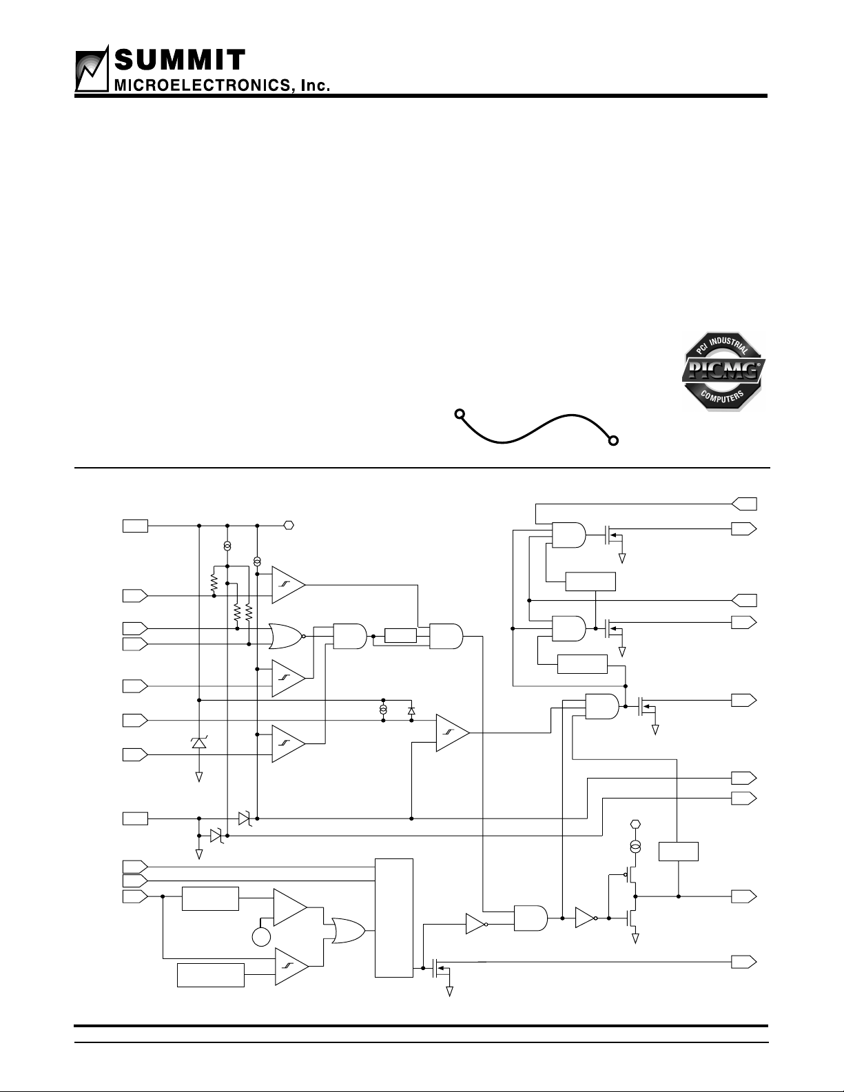
FUNCTIONAL BLOCK DIAGRAM
ASSOCIATE
MEMBER
P
r
o
g
r
a
m
m
a
b
l
e
Q
u
i
c
k
-
T
r
i
p
TM
C
i
r
c
u
i
t
B
r
e
a
k
e
r
F
eaturing
+
-
+
-
+
-
12V
5V
2.5V
Programmable
Delay
Programmable
Delay
+
-
+
-
CBFault#
2041 BD 8.0
Vgate
2.5V ref
5.0V ref
PG1#
PG2#
ENPGB
ENPGA
PG3#
CBSense
Programmable
Delay
VSS
CBMode
CBReset#
EN/TS
PD1#
PD2#
UV
OV
Drain
Sense
VDD
Fault
Latch
&
Duty
Cycle
Timer
+
-
50
mV
Programmable
Quick-Trip
Ref Voltage
Filter
12V ref
12V
current limit
Vgate
Sense
50kΩ
50kΩ
50kΩ
2
SMH4803
2041 8.4 6/15/00
SUMMIT MICROELECTRONICS
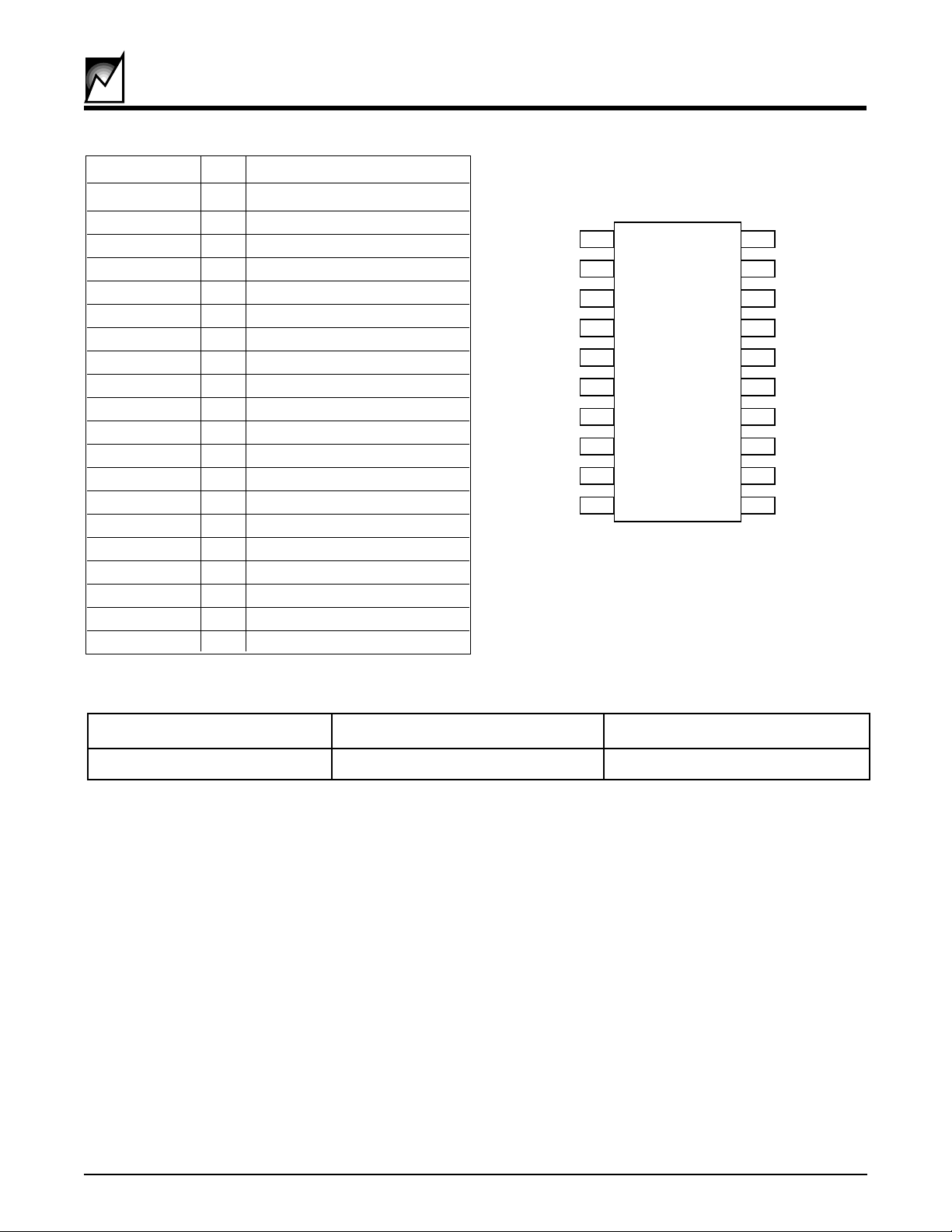
Symbol Pin Description
Drain Sense 1 Drain sense input
Vgate 2 Output to MOSFET gate
EN/TS 3 Enable/Temp Sense input
PD1# 4 Pin Detect 1 (active LO)
PD2# 5 Pin Detect 2 (active LO)
CBFault# 6 Circuit Breaker Fault output
CBReset# 7 Circuit Breaker Reset intput
CBMode 8 Circuit Breaker Mode control
CBSense 9 Cicruit Breaker Sense input
Vss 10 Negative Supply Connection
UV 11 Under Voltage input
OV 12 Over Voltage input
5V 13 5V reference output
2.5V 14 2.5V reference output
ENPGB 15 Enable input B
ENPGA 16 Enable input A
PG3# 17 Power good output 3
PG1# 18 Power good output 1
PG2# 19 Power good output 2
Vdd 20 Positive supply connection
2041 PGM T2.1
PIN CONFIGURATIONS
RECOMMENDED OPERATING CONDITIONS
Condition Min Max
Temperature -40°C +85°C
2041 PGM T3.0
1
2
3
4
5
6
7
8
9
10
16
15
14
13
12
11
19
20
17
18
2041 ILL10.1
Drain Sense
Vgate
EN/TS
PD1#
PD2#
CBFault#
CBReset#
CBMode
CBSense
Vss
Vdd
PG2#
PG1#
PG3#
ENPGA
ENPGB
2.5V
5V
OV
UV
DESCRIPTION
The SMH4803 is designed to control hot swapping of
plug-in cards operating from a single supply ranging from
20V to 500V. The SMH4803 hot-swap controller provides
under-voltage and over-voltage monitoring of the host
power supply, it drives an external power MOSFET switch
that connects the supply to the load, and also protects
against over-current conditions that might disrupt the host
supply. When the input and output voltages to the
SMH4803 controller are within specification, the
SMH4803 provides three “Power Good” logic outputs that
may be used to turn ON the loads, e.g. isolated-output DC-
DC converters, or drive LED status lights. The SMH4803
provides three separate “Power Good” logic outputs that
activate loads in a timed sequence. Additional features of
the SMH4803 include: temperature sense or master en-
able input, 2.5V and 5V reference outputs for expanding
monitor functions, two “Pin-Detect” enable inputs for fault
protection, and duty-cycle or latched over-current protec-
tion modes.
3
2041 8.4 6/15/00
SMH4803
SUMMIT MICROELECTRONICS
*COMMENT
Stresses listed under Absolute Maximum Ratings
may cause permanent damage to the device. These
are stress ratings only, and functional operation of
the device at these or any other conditions outside
those listed in the operational sections of this speci-
fication is not implied. Exposure to any absolute
maximum rating for extended periods may affect
device performance and reliability.
ABSOLUTE MAXIMUM RATINGS
Temperature Under Bias -55°C to +125°C
Storage Temperature -65°C to +150°C
Voltage on pins with respect to V
SS
Vdd -0.5V to Vdd
UV, OV, CBSense, Drain Sense -0.5V to Vdd +0.5V
PD1#, PD2#, CBMode, CBReset# 10V
ENPGA, ENPGB, EN/TS
CBFault#, PG1#, PG2#, PG3# -0.5V to Vdd +0.5V
Vgate Vdd + 0.5V
Lead Solder Temperature (10 secs) 300 °C
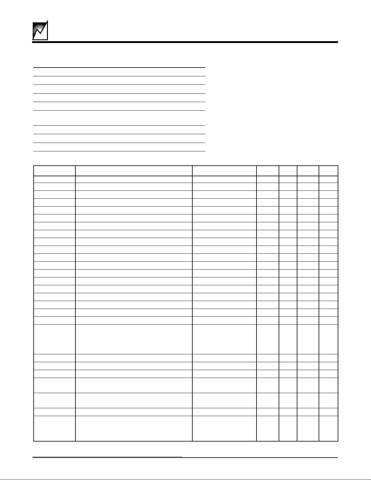
Symbol Parameter Notes Min. Typ. Max. Units
V
DD
Supply Voltage I
DD
= 2mA 11 12 13 V
Vref5 5Volt Reference Output I
DD
= 2mA 4.7 5 5 5.25 V
I
LOAD5
5Volt Reference Output Current I
DD
= 2mA -1 1 mA
Vref2.5 2.5 Volt Reference Output T
A
= 25 °C, I
DD
= 2mA 2.475 2.5 2.525 V
Vref2.5 2.5 Volt Reference Output I
DD
= 2mA 2.425 2.5 2.575 V
I
LOAD2.5
2.5 Volt Reference Output Current I
DD
= 2mA -0.2 1 mA
I
DD
Power Supply Current Output Enabled 2 10 mA
V
UV
Under voltage Threshold T
A
= 25 °C, I
DD
= 2mA 2.475 2.5 2.525 V
V
UV
Under voltage Threshold I
DD
= 2mA 2.425 2.5 2.575 V
V
UVHYS
Under voltage Hysteresis I
DD
= 2mA 10 mV
V
OV
Over voltage Threshold T
A
= 25 °C, I
DD
= 2mA 2.475 2.5 2.525 V
V
OV
Over voltage Threshold I
DD
= 2mA 2.425 2.5 2.575 V
V
OVHYS
Over voltage Hysteresis I
DD
= 2mA 10 mV
V
VGATE
Vgate Output Voltage V
DD
V
I
VGATE
Vgate Current Output 100 µ A
V
SENSE
Drain Sense threshold T
A
= 25 °C, I
DD
= 2mA 2.475 2.5 2.525 V
V
SENSE
Drain Sense threshold I
DD
= 2mA 2.425 2.5 2.575 V
I
SENSE
Drain Sense Output Current (Note 1) V
SENSE
= V
SS
91011µA
V
CB
Circuit Breaker Threshold I
DD
= 2mA 40 50 60 mV
V
QCB
Quick-Trip Circuit Breaker Threshold
Option E
200 mV
Option F
100 mV
Option H
50 mV
Option J
OFF
V
ENTS
EN/TS Threshold T
A
= 25 °C, I
DD
= 2mA 2.425 2.5 2.575 V
V
ENTS
EN/TS Threshold I
DD
= 2mA 2.475 2.5 2.525 V
V
ENTSHYS
EN/TS Hysteresis I
DD
= 2mA 5 10 15 mV
V
IH
Input High Voltage ENPGA/B, 2 Vref5 V
CBMode, CBReset#
V
IL
Input High Voltage ENPGA/B, -0.1 0.8 V
CBMode, CBReset#
V
OL
CBFault# Output Low Voltage I
OL
= 2mA 0 0.4 V
V
OL
PG1#, PG2#, PG3# Output Low I
SINK
= 2mA 0 0.4 V
DC OPERATING CHARACTERISTICS (Over Recommended Operating Conditions, Voltages are relative to V
SS
)
2041 PGM T4.4
(Note 1) : T
A
= 25 °C
4
SMH4803
2041 8.4 6/15/00
SUMMIT MICROELECTRONICS
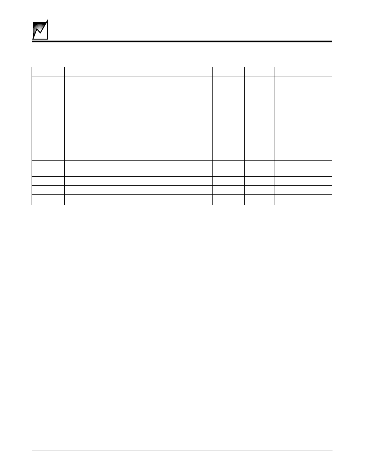
AC Timing Characteristics, -40
o
C to +85
o
C
Symbol Description Min. Typ. Max Unit
t
PDD
Pin Detect Delay to Vgate enable 80 ms
t
CBD
50mv Circuit Breaker Delay (Filter)
K 400 µs
L 150 µs
M50µs
N5µs
P
GD
Power Good Delay (PG1/PG2, PG2/PG3)
A5ms
B20ms
C80ms
D 180 ms
t
FSTSHTDN
Fast Shut Down Delay From Fault to 200 ns
Vgate Off
t
CYC
Circuit Breaker Cycle Mode Cycle Time 2.5 Sec.
t
VGD
Delay from Release of Reset to Vgate on 100 ns
t
CBRST
CBReset# Pulse Width 200 ns
5
2041 8.4 6/15/00
SMH4803
SUMMIT MICROELECTRONICS
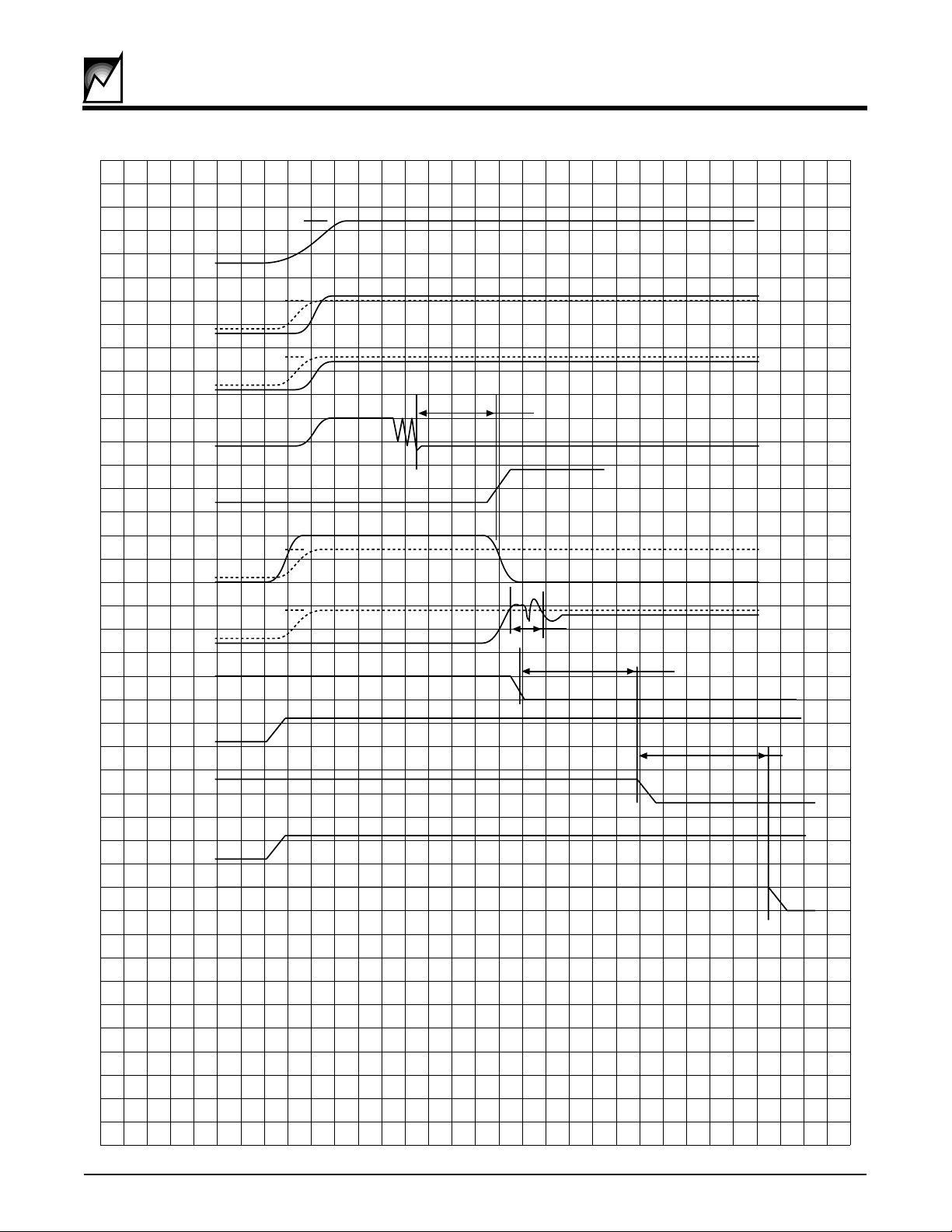
≥11V≤13V
2.5V ref
2.5V ref
VDD
UV
OV
PD1#/PD2#
tPDD
Vgate
2.5V ref
Drain
Sense
50mV ref
CBSense
PG1#
ENPGA
PG2#
ENPGB
PG3#
<tCBD
PGD
PGD
2041 ILL18.0
Figure 1. Power Sequencing Timing Characteristics
6
SMH4803
2041 8.4 6/15/00
SUMMIT MICROELECTRONICS
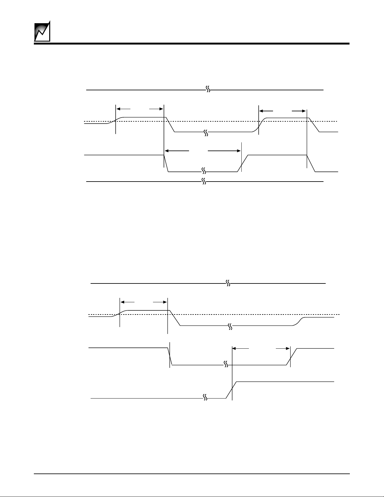
Figure 2. Circuit Breaker Timing - Cycle Mode, CBReset# Held High
CBMode
CBSense
Vgate
CBReset#
V
IH
t
CBD
t
CYC
t
CBD
V
IH
50mV
2041 ILL16.0
Figure 3. Circuit Breaker Timing - Cycle Mode, Used to Enable Vgate
CBMode
CBSense
Vgate
CBReset#
V
IH
t
CBD
V
IL
t
CYC
50mV
2041 ILL17.0

7
2041 8.4 6/15/00
SMH4803
SUMMIT MICROELECTRONICS
Figure 4. Circuit Breaker Timing - Reset Mode
Figure 5. Circuit Breaker Timing - Quick-Trip
CBMode
CBSense
Vgate
CBReset#
VIL
tCBD
tCBRST
tVGD
50mV
2041 ILL14.0
CBSense
Vgate
<t
CBD
t
FSTSHTDN
50mV
QCB
V
2041 ILL15.0
 Loading...