

Page 1
1
STC03DE170HV
HYBRID EMITTER SWITCHED BIPOLAR TRANSISTOR
ESBT™ 1700 V - 3 A - 0.55 W
Table 1: General Features
V
CS(ON)
1 V 1.8 A 0.55 W
n LOW EQUIVALENT ON RESISTANCE
n VERY FAST-SWITCH, UP TO 150 kHz
n SQUARED RBSOA, UP TO 1700 V
n VERY LOW C
I
C
DRIVEN BY RG = 4.7 W
ISS
R
CS(ON)
APPLICATION
n AUX SMPS FOR THREE PHASE MAINS
DESCRIPTION
The STC03DE170HV is manufactured in a hybrid
structure, using dedicated high voltage Bipolar
and low voltage MOSFET technologies, aimed to
providing the best performance in ESBT topology.
The STC03DE170HV is designed for use in aux
flyback smps for any three phase application.
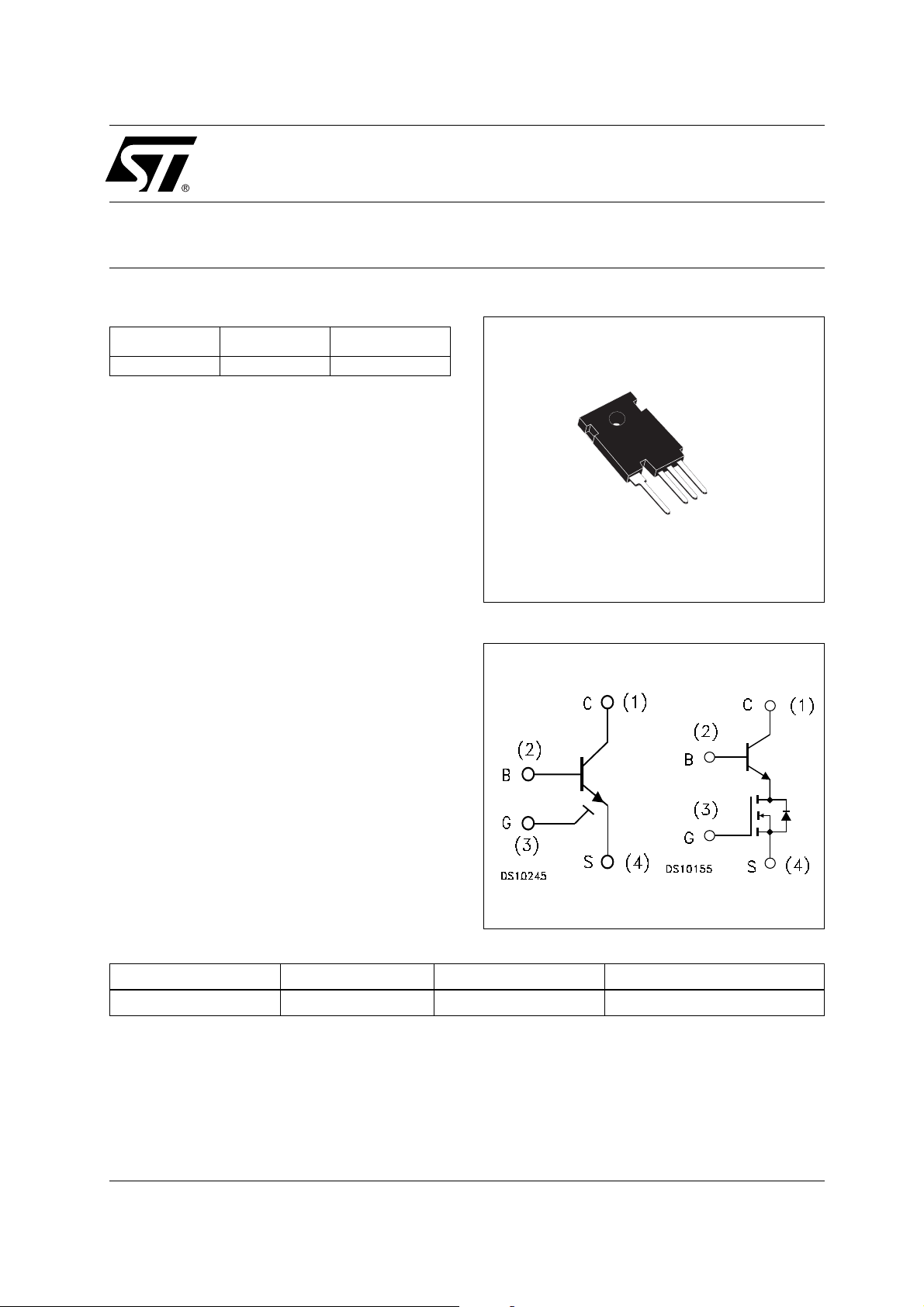
Figure 1: Package
4
3
2
TO247-4L HV
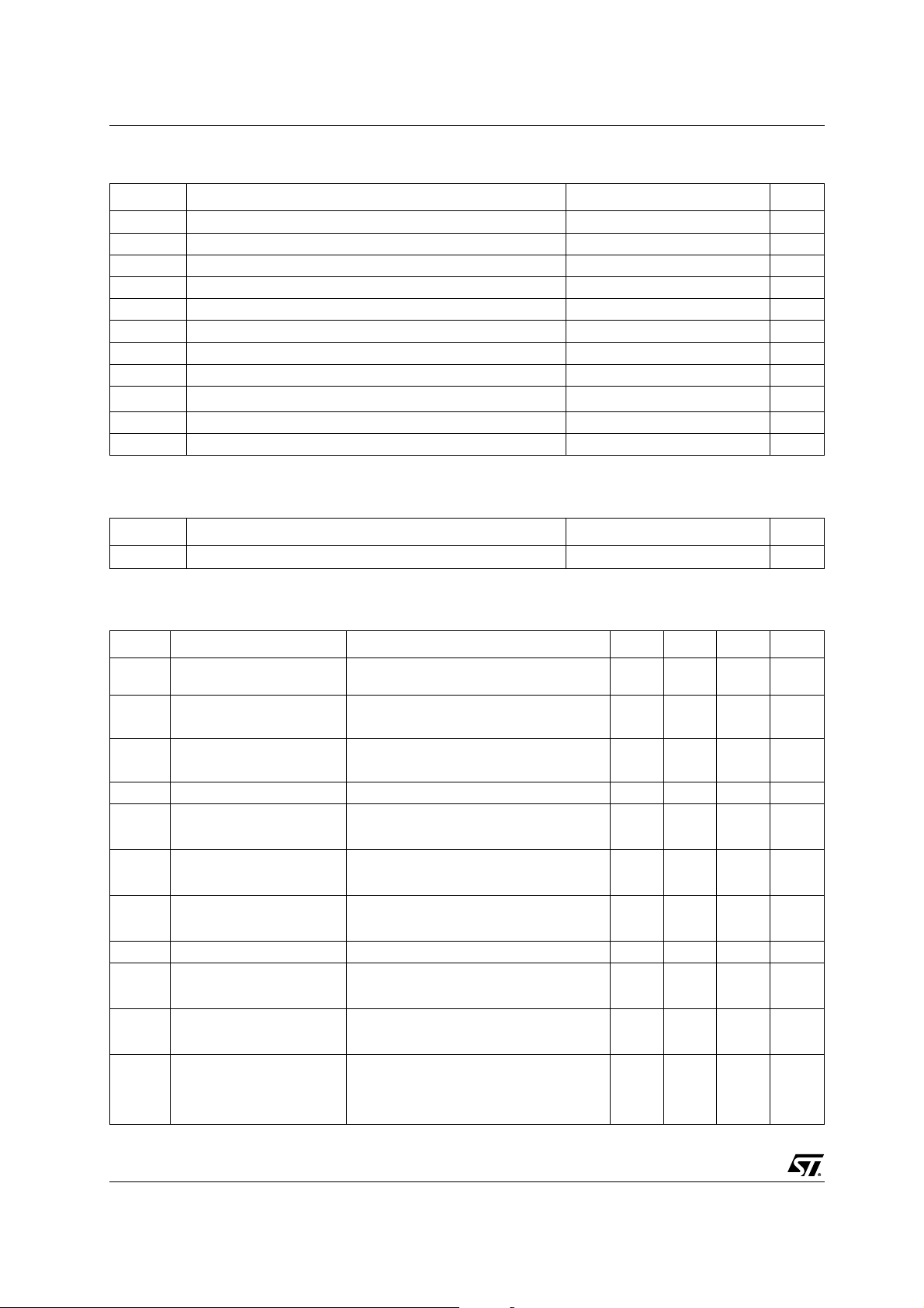
Figure 2: Internal Schematic Diagram
Table 2: Order Code
Part Number Marking Package Packaging
STC03DE170HV C03DE170HV TO247-4L HV TUBE
Electrical Symbol Device Structure
Rev. 1
1/9January 2005
Page 2
STC03DE170HV
Table 3: Absolute Maximum Ratings
Symbol Parameter Value Unit
V
CS(SS)
V
BS(OS)
V
SB(OS)
V
I
I
CM
I
I
BM
P
T
stg
T
Table 4: Thermal Data
Symbol Parameter Unit
R
thj-case
Collector-Source Voltage (VBS = VGS = 0 V)
Base-Source Voltage (IC= 0, VGS = 0 V)
Source-Base Voltage (IC= 0, VGS = 0 V)
Gate-Source Voltage
GS
Collector Current
C
Collector Peak Current (tp < 5ms)
Base Current
B
Base Peak Current (tp < 1ms)
Total Dissipation at TC = 25 oC
tot
Storage Temperature
Max. Operating Junction Temperature
J
Thermal Resistance Junction-Case Max 1
1700 V
30 V
9V
± 20 V
3A
6A
2A
4A
100 W
-65 to 125 °C
125 °C
o
C/W
Table 5: Electrical Characteristics (T
= 25 oC unless otherwise specified)
case
Symbol Parameter Test Conditions Min. Typ. Max. Unit
I
CS(SS)
I
BS(OS)
I
SB(OS)
I
GS(OS)
V
CS(ON)
V
BS(ON)
V
Q
Collector-Source Current
(V
= VGS = 0 V)
BS
Base-Source Current
(I
= 0 , VGS = 0 V)
C
Source-Base Current
= 0 , VGS = 0 V)
(I
C
V
V
V
= 1700 V 100 mA
CS(SS)
= 30 V 10 mA
BS(OS)
= 9 V 100 mA
SB(OS)
Gate-Source Leakage VGS = ± 20 V 500 nA
Collector-Source ON
Voltage
DC Current Gain IC = 1.8 A VCS = 1 V VGS = 10 V
h
FE
Base-Source ON Voltage VGS = 10 V IC = 1.8 A IB = 0.36 A
Gate Threshold Voltage VBS = VGS IB = 250 mA1.52.23V
GS(th)
Input Capacitance VCS = 25 V f = 1MHZ
C
iss
Gate-Source Charge VCS = 15 V VGS = 10 V
GS(tot)
INDUCTIVE LOAD
t
Storage Time
s
t
Fall Time
f
VGS = 10 V IC = 1.8 A IB = 0.36 A
V
= 10 V IC = 0.7 A IB = 70 mA
GS
I
= 0.7 A VCS = 1 V VGS = 10 V
C
V
= 10 V IC = 0.7 A IB = 70 mA
GS
V
= VCB = 0
GS
V
= 0 IC = 1.8 A
CB
VGS = 10 V
R
= 47 W V
G
t
= 4 ms IC = 1.8 A IB = 0.36 A
p
Clamp
= 1200 V
3.5
6
1
1.5
1
1.3
5
10
1
1.2
0.8
1
750 pF
12.5 nC
760
14
V
V
V
V
ns
ns
2/9
Page 3
STC03DE170HV
Symbol Parameter Test Conditions Min. Typ. Max. Unit
t
V
CSW
V
CS(dyn)
V
CS(dyn)
INDUCTIVE LOAD
Storage Time
s
t
Fall Time
f
Maximum Collector-Source
Voltage Switched Without
Snubber
Collector-Source Dynamic
Voltage
(500 ns)
Collector-Source Dynamic
Voltage
(1ms)
VGS = 10 V
R
= 47 W V
G
t
= 4 ms IC = 0.7 A IB = 70 mA
p
Clamp
= 1200 V
690
32
RG = 47 W hFE = 5 A IC = 3 A 1500 V
VCC = V
R
= 47 W IC = 0.5 A
G
I
= 0.1 A I
B
t
= 500 ns
peak
VCC = V
R
= 47 W IC = 0.5 A
G
I
= 0.1 A I
B
t
= 500 ns
peak
= 400 V VGS = 10 V
Clamp
= 400 V VGS = 10 V
Clamp
Bpeak
Bpeak
= 1 A
= 1 A
3.9 V
2.2 V
ns
ns
3/9
Page 4

STC03DE170HV
Figure 3: Safe Operating Area
Figure 4: Reverse Biased Safe Operating Area
Figure 6: Output Characteristics
Figure 7: Gate Threshold Voltage vs Temperature
Figure 5: DC Current Gain
4/9
Figure 8: DC Current Gain
Page 5

STC03DE170HV
Figure 9: Collector-Source On Voltage
Figure 10: Base-Source On Voltage
Figure 12: Collector-Source On Voltage
Figure 13: Base-Source On Voltage
Figure 11: Inductive Load Switching Time
Figure 14: Inductive Load Switching Time
5/9
Page 6

STC03DE170HV
Figure 15: Dynamic Collector-Emitter Saturation Voltage
Figure 16: Inductive Load Enlargement FBSOA Circuit
Table 6: Components, Values
VB1 = 4.16 V
D
= BA157
1
R
= 1 W
1
R
= 100 W
2
R
= V
3
CC
Rg = 47 W
6/9
/ I
Cn
C
= 220 nF
1
C
≤ 70 pF
2
C
= 50 nF
3
V
= 10 V
g
Pulse Time = 5 ms
Page 7

DIM.
mm.
MIN. TYP MAX.
A 4.85 5.15
A1 2.20 2.50 2.60
A2 1.27
b
0.95
1.10 1.30
b2 2.50 2.90
c 0.40 0.80
D 23.85 24 24.15
D1 21.50
E 15.45 15.60 15.75
e2.54
e1 5.08
L 10.20 10.80
L1 2.20 2.50 2.80
L2 18.50
L3 3
øP 3.55 3.65
S5.50
TO247-4L HV MECHANICAL DATA
7734874
STC03DE170HV
7/9
Page 8

STC03DE170HV
Table 7: Revision History
Date Release Change Designator
21-Jan-2005 1 First Release.
8/9
Page 9

STC03DE170HV
Information furnished is believed to be accurate and reliable. However, STMicroelectronics assumes no responsibility for the consequences
of use of suc h inf ormati on nor for a ny i nfring eme nt o f p atent s or o t her ri ghts of t hird par ties wh ich m ay res ul t from i ts us e. No license is gr an ted
by implication or otherwise under any patent or patent rights of STMicroelectronics. Specifications mentioned in this publication are subject
to change without notice. This publication supersedes and replaces all information previously supplied. STMicroelectronics products are not
authorized for use as critical components in life support devices or systems without express written approval of STMicroelectronics.
The ST logo is a registered trademark of STMicroelectronics
All other names are the property of their respective owners
© 2005 STMicroelectronics- All Rights Reserved
STMicroelectronics group of companies
Australia - Belgium - Brazil - Canada - China - Czech Republic - Finland - France - Germany - Hong Kong - India - Israel - Italy - Japan -
Malaysia - Malta - Morocco - Singapore - Spain - Sweden - Switzerland - United K ingdom - United States of America
www.st.com
9/9
 Loading...