

Page 1
STC6602
Dual N&P Channel Enhancement Mode
MOSFET
2.8A/-2.8A
DESCRIPTION
The STC6602 is the dual N&P-Channel enhancement mode power field effect transistor
which is produced using high cell density, DMOS trench technology. This high density
process is especially tailored to minimize on-state resistance. These devices are particularly
suited for low voltage application, such as notebook computer power management and
other battery powered circuits, where high-side switching is required.
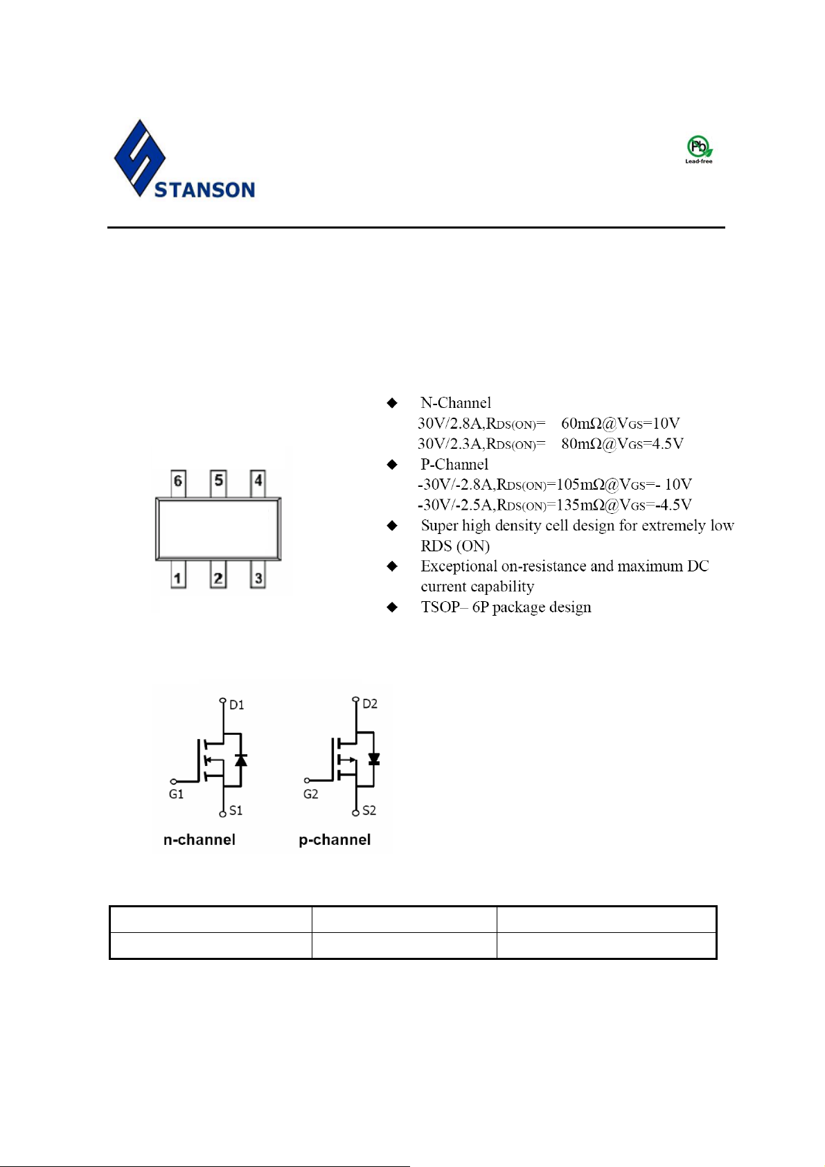
PIN CONFIGURATION
TSOP-6
D1 S1 D2
FEATURE
02YW
G1 S2 G2
Y: Year
A: Week Code
ORDERING INFORMATION
Part Number Package Part Marking
STC6602ST6RG TSOP-6 02YW
※ Week Code Code : A ~ Z ; a ~ z
※ STC6602ST6RG ST6 : TSOP-6; R: Tape Reel ; G: Pb – Free
STANSON TECHNOLOGY
120 Bentley Square, Mountain View, Ca 94040 USA
http://www.stansontech.com
STC6602 2007. V1
Page 2
STC6602
Dual N&P Channel Enhancement Mode
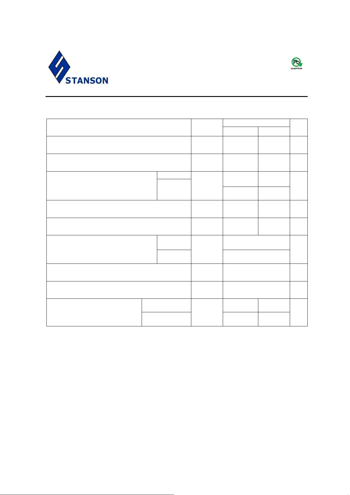
ABSOULTE MAXIMUM RATINGS (Ta = 25 Unless otherwise noted )℃
Parameter Symbol
Drain-Source Voltage V
30 -30 V
DSS
Typical
N P
MOSFET
2.8A/-2.8A
Unit
Gate-Source Voltage V
GSS
±20
±20
V
=150 )℃
(T
J
TA=25℃ 2.8 -2.8 Continuous Drain Current
=70℃
T
A
I
D
A
2.3 -2.1
Pulsed Drain Current IDM 10 -8 A
Continuous Source Current (Diode Conduction)
Power Dissipation
TA=25℃ 1.15
=70℃
T
A
IS 1.25 -1.4 A
P
D
W
0.75
Operation Junction Temperature TJ -55/150 ℃
Storage Temperature Range T
Thermal Resistance-Junction
T≦10sec
to Ambient
Steady State
-55/150 ℃
STG
R
θJA
50 52
90 90
/W℃
STANSON TECHNOLOGY
120 Bentley Square, Mountain View, Ca 94040 USA
http://www.stansontech.com
STC6602 2007. V1
Page 3
Dual N&P Channel Enhancement Mode
nA
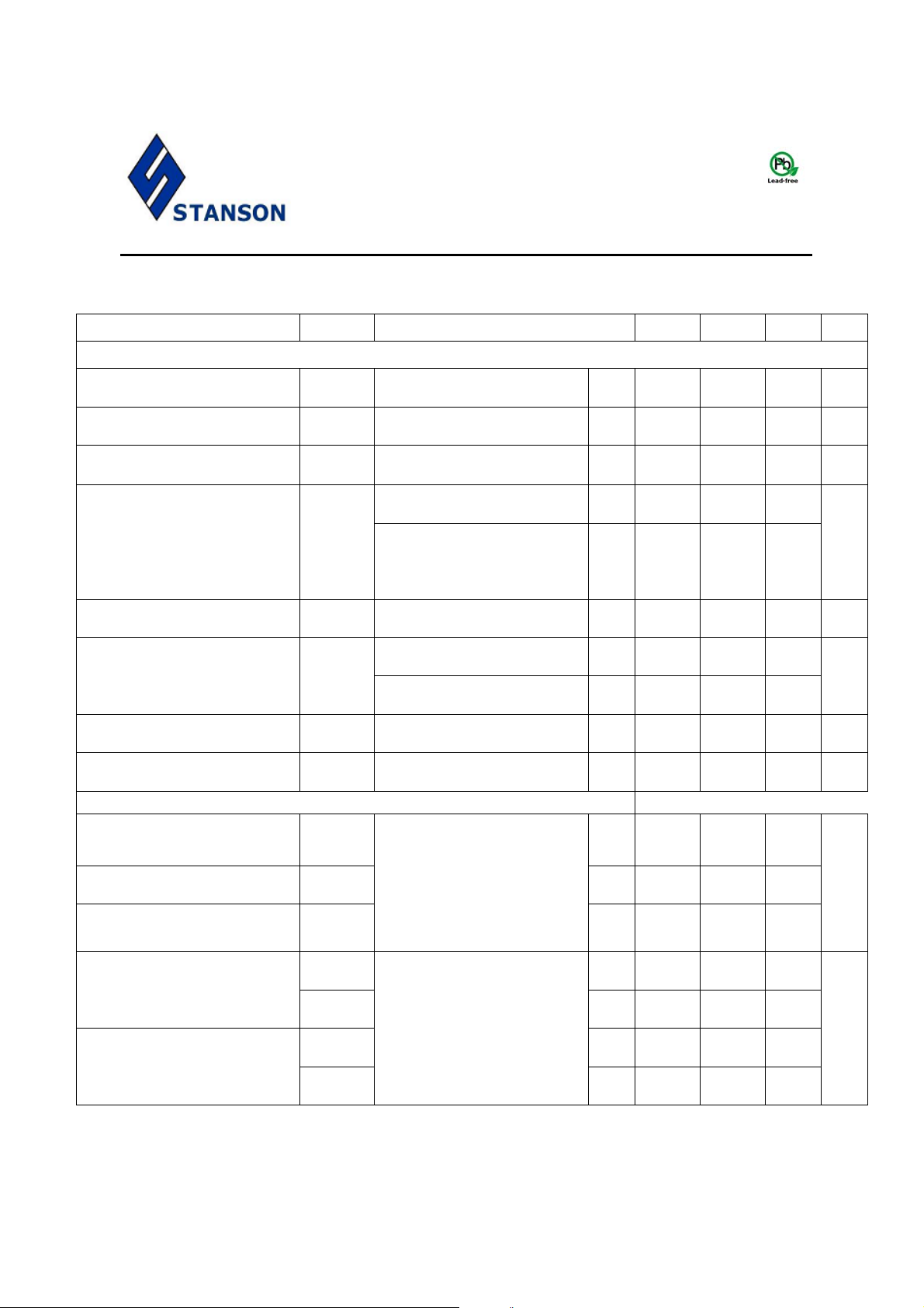
ELECTRICAL CHARACTERISTICS ( Ta = 25 Unless otherwise noted )℃
Parameter Symbol
Condition Min Typ Max Unit
Static
STC6602
MOSFET
2.8A/-2.8A
Drain-Source Breakdown
Voltage
Gate Threshold Voltage V
Gate Leakage Current I
Zero Gate Voltage Drain
Current
On-State Drain Current I
Drain-source On-Resistance
Forward Transconductance gfs V
Diode Forward Voltage VSD I
V
(BR)DSS
GS(th)
GSS
I
DSS
D(on)
R
DS(on)
VGS=0V,ID=250uA
=0V,ID=-250uA
V
GS
VDS=VGS,ID=250uA
=VGS,ID=-250uA
V
DS
V
=0V,VGS=±20V
V
DS
VDS=30V,VGS=0V
=-30V,VGS=0V
V
DS
V
=30V,VGS=0V
DS
=55℃
T
J
=-30V,VGS=0V
V
DS
=55℃
T
J
≦5V,VGS=10V
DS
≦-5V,VGS=-10V
V
DS
VGS=10V,ID=2.8A
=-10V,ID=-2.8A
V
GS
=4.5V,ID=2.3A
V
GS
=-4.5V,ID=-2.5A
V
GS
=10V,ID=2.8A
DS
=-10V,ID=-2.8A
V
DS
=1.25A,VGS=0V
S
=-1.2A,VGS=0V
I
S
N
p
N
P
N
p
N
P
N
P
30
V
-30
1
1
±100
10
6
-6
0.043
0.088
0.056
0.118
4.6
-4
0.8
-0.8
3
-3
±100
1
-1
-10
0.060
0.105
0.080
0.135
1.2
-1.2
V
uA
A
Ω
S
V
Dynamic
Total Gate Charge Qg
Gate-Source Charge Qgs N
Gate-Drain Charge Qgd
N-Channel
=15V,VGS=4.5V,
V
DS
V
=2.0A
DS
P-channel
=-15V,VGS=-4.5V,
V
DS
=-2.0A
V
N
P
P
N
P
4.5
5.8
0.8
0.8
1.0
1.5
10
10
nC
Turn-On Time
Turn-Off Time
T
N
d(on)
N-Channel
N
t
r
T
N
d(off)
t
f
DD=15V, RL=10Ω,
V
GEN=10V, RG=3Ω
V
P-Channel
DD=-15V, RL=15Ω,
V
GEN=-10V, RG=3Ω
V
8
P
12
P
9
17
P
N
P
8
18
6
9
20
20
30
20
35
35
20
20
nS
STANSON TECHNOLOGY
120 Bentley Square, Mountain View, Ca 94040 USA
http://www.stansontech.com
STC6602 2007. V1
Page 4
STC6602
Dual N&P Channel Enhancement Mode
MOSFET
2.8A/-2.8A
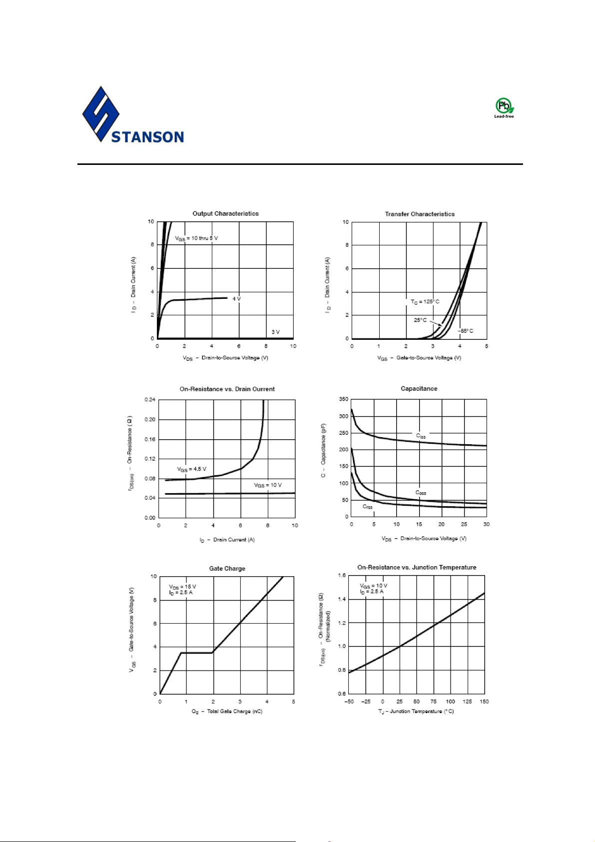
TYPICAL CHARACTERICTICS ( N-Channel )
STANSON TECHNOLOGY
120 Bentley Square, Mountain View, Ca 94040 USA
http://www.stansontech.com
STC6602 2007. V1
Page 5
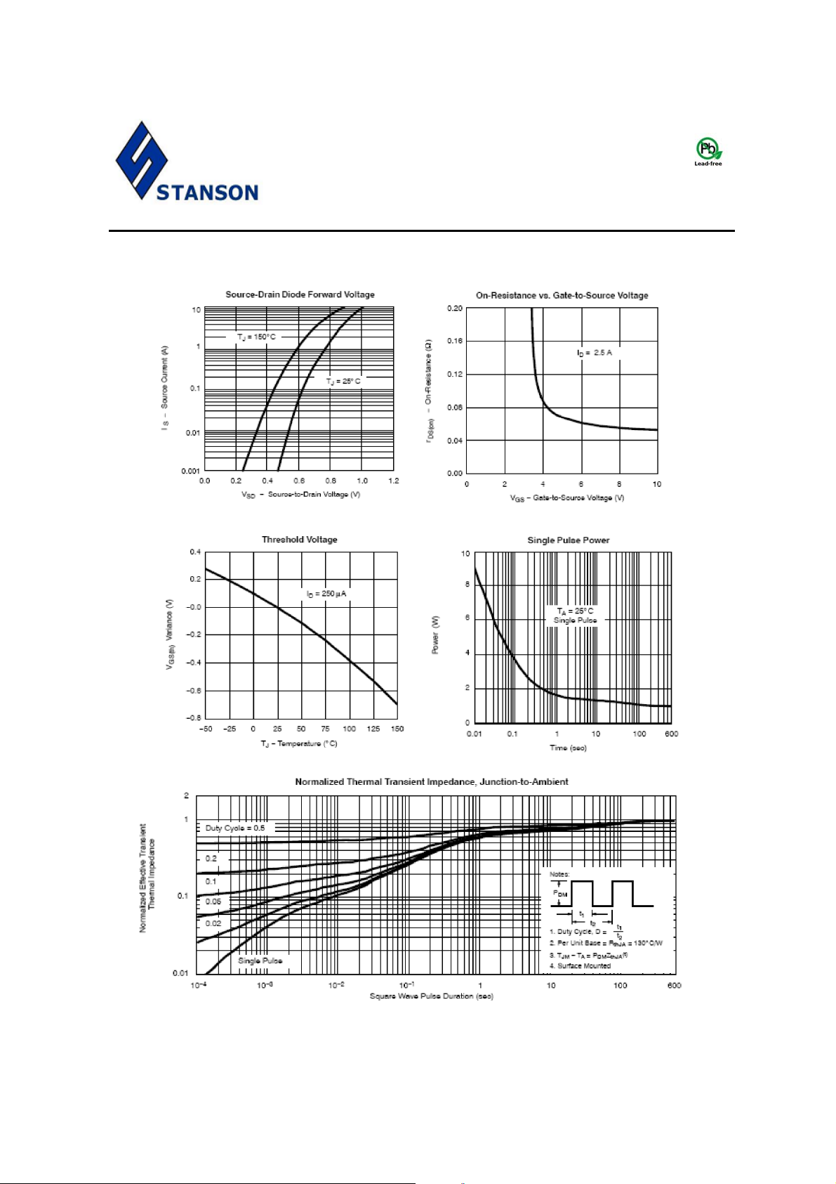
TYPICAL CHARACTERICTICS ( N-Channel )
STC6602
Dual N&P Channel Enhancement Mode
MOSFET
2.8A/-2.8A
STANSON TECHNOLOGY
120 Bentley Square, Mountain View, Ca 94040 USA
http://www.stansontech.com
STC6602 2007. V1
Page 6
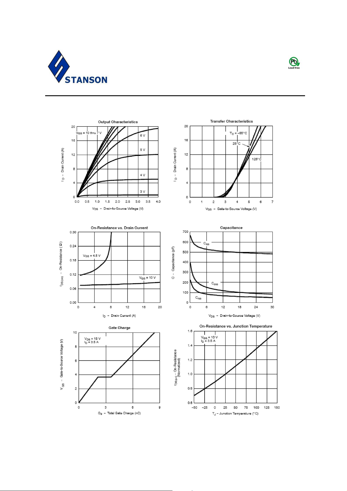
TYPICAL CHARACTERICTICS ( P-Channel )
STC6602
Dual N&P Channel Enhancement Mode
MOSFET
2.8A/-2.8A
STANSON TECHNOLOGY
120 Bentley Square, Mountain View, Ca 94040 USA
http://www.stansontech.com
STC6602 2007. V1
Page 7
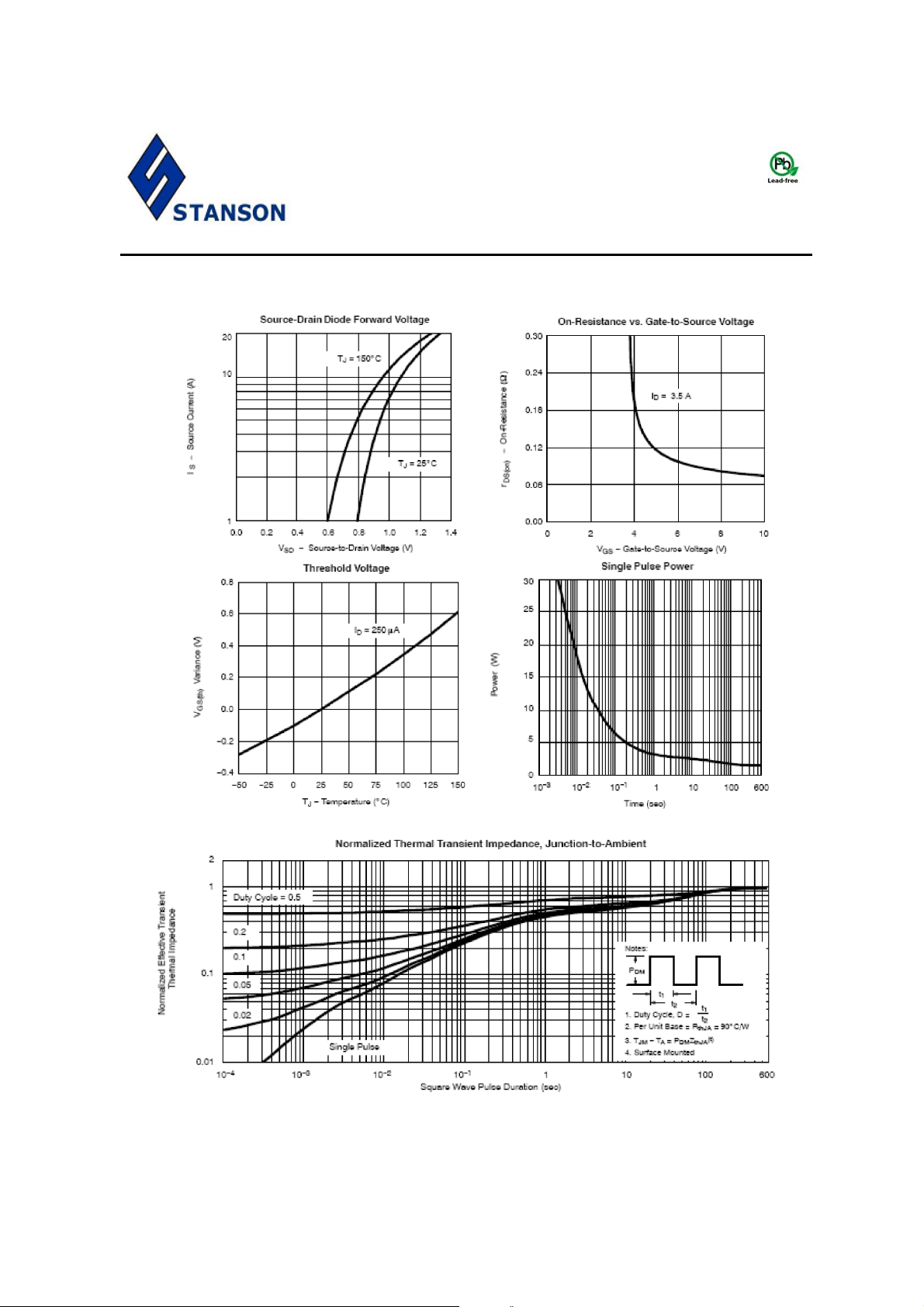
TYPICAL CHARACTERICTICS ( P-Channel )
STC6602
Dual N&P Channel Enhancement Mode
MOSFET
2.8A/-2.8A
STANSON TECHNOLOGY
120 Bentley Square, Mountain View, Ca 94040 USA
http://www.stansontech.com
STC6602 2007. V1
Page 8
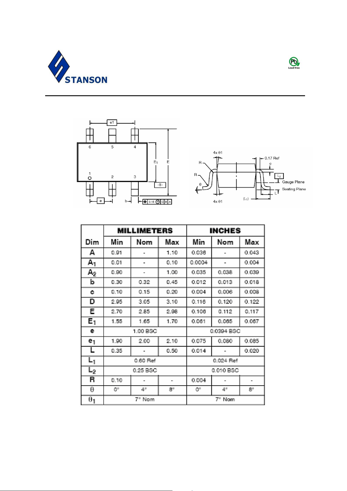
TSOP-6 PACKAGE OUTLINE
STC6602
Dual N&P Channel Enhancement Mode
MOSFET
2.8A/-2.8A
STANSON TECHNOLOGY
120 Bentley Square, Mountain View, Ca 94040 USA
http://www.stansontech.com
STC6602 2007. V1
Page 9

 Loading...