

Page 1
512 Bit (64 bit x8) SERIAL RTC (SPI) SRAM
FEATURES SUMMARY
■ 2.7 TO 5.5V OPERATING V OLT AGE
■ SERIAL PERIPHERAL INTERFACE (SPI)
■ 2.5 TO 5.5V OSCILLATOR OPERATING
VOLTAGE
■ AUTOMATIC SWITCH-OVER and DESELECT
CIRCUITRY
■ CHOICE OF POWER-FAIL DESELECT
VOLTAGES (V
–THS = V
–THS = V
■ COUNTERS FOR TENTHS/HUNDREDTHS
OF SECONDS, SECONDS, MINUTES,
HOURS, DAY, DATE , MONTH, YEAR, and
CENTURY
■ 44 BYTES OF GENERAL PURPOSE RAM
■ PROGRAMMABLE ALARM and INTE RRUPT
FUNCTION (VALID EVEN DURING BATTERY
BACK-UP MODE)
■ WATCHDOG T IME R
■ MICROPROCESSOR POWER-ON RESET
■ BATTERY LOW FLAG
■ LOW OPERATING CURRENT OF 2.0mA
■ ULTRA-LOW BATTER Y SUPPL Y C U RRE NT
OF 500nA (MAX)
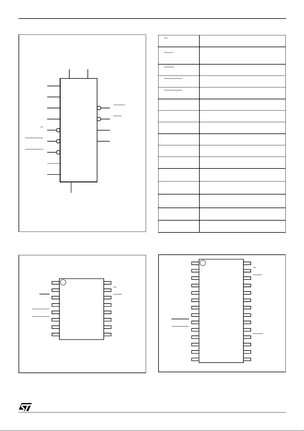
■ PACKAGING INCLUD ES A 28-LEAD SOIC and
SNAPHAT
®
16-LEAD SOIC
■ 28-LEAD SOIC PACKAGE PROVIDES
DIRECT CONNECTION FOR A SNAPHAT
TOP WHICH CONTAINS THE BATTERY and
CRYSTAL
= 2.7 to 5.5V):
CC
; 2.55V ≤ V
SS
; 4.20V ≤ V
CC
PFD
PFD
≤ 2.70V
≤ 4.50V
TOP (to be ordered separately) or
M41T94
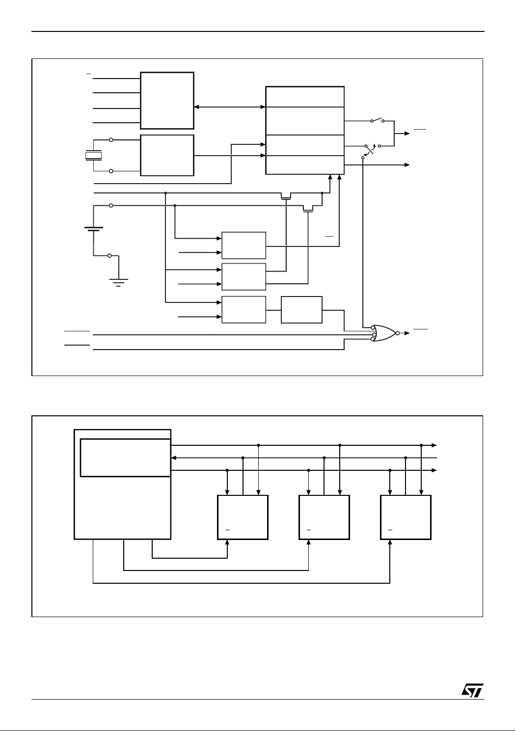
Figure 1. 16-pi n S O I C Package
16
1
SO16 (MQ)
Figure 2. 28-pi n S O I C Package
SNAPHAT (SH)
Battery & Crystal
28
1
SOH28 (MH)
Rev. 2.0
1/31June 2003
Page 2

M41T94
TABLE OF CONTENTS
SUMMARY DESCRIPTION. . . . . . . . . . . . . . . . . . . . . . . . . . . . . . . . . . . . . . . . . . . . . . . . . . . . . . . . . . . 4
Figure 3. Logic Diagram . . . . . . . . . . . . . . . . . . . . . . . . . . . . . . . . . . . . . . . . . . . . . . . . . . . . . . . . . . 5
Table 1. Signal Names . . . . . . . . . . . . . . . . . . . . . . . . . . . . . . . . . . . . . . . . . . . . . . . . . . . . . . . . . . . 5
Figure 4. 16-pin SOIC Connections. . . . . . . . . . . . . . . . . . . . . . . . . . . . . . . . . . . . . . . . . . . . . . . . . . 5
Figure 5. 28-pin SOIC Connections. . . . . . . . . . . . . . . . . . . . . . . . . . . . . . . . . . . . . . . . . . . . . . . . . . 5
Figure 6. Block Diagram . . . . . . . . . . . . . . . . . . . . . . . . . . . . . . . . . . . . . . . . . . . . . . . . . . . . . . . . . . 6
Figure 7. Hardware Hookup . . . . . . . . . . . . . . . . . . . . . . . . . . . . . . . . . . . . . . . . . . . . . . . . . . . . . . . 6
Table 2. Function Table . . . . . . . . . . . . . . . . . . . . . . . . . . . . . . . . . . . . . . . . . . . . . . . . . . . . . . . . . . . 7
Signal Description. . . . . . . . . . . . . . . . . . . . . . . . . . . . . . . . . . . . . . . . . . . . . . . . . . . . . . . . . . . . . . 7
MAXIMUM RATING. . . . . . . . . . . . . . . . . . . . . . . . . . . . . . . . . . . . . . . . . . . . . . . . . . . . . . . . . . . . . . . . . 8
Table 3. Absolute Maximum Ratings. . . . . . . . . . . . . . . . . . . . . . . . . . . . . . . . . . . . . . . . . . . . . . . . . 8
DC AND AC PARAMETERS. . . . . . . . . . . . . . . . . . . . . . . . . . . . . . . . . . . . . . . . . . . . . . . . . . . . . . . . . . 9
Table 4. DC and AC Measurement Conditions . . . . . . . . . . . . . . . . . . . . . . . . . . . . . . . . . . . . . . . . . 9
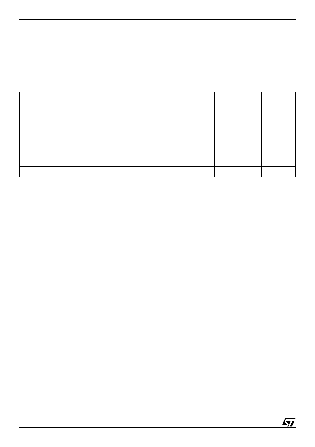
Figure 9. AC Testing Input/Output Waveforms . . . . . . . . . . . . . . . . . . . . . . . . . . . . . . . . . . . . . . . . . 9
Table 5. Capacitance. . . . . . . . . . . . . . . . . . . . . . . . . . . . . . . . . . . . . . . . . . . . . . . . . . . . . . . . . . . . . 9
Table 6. DC Characteristics. . . . . . . . . . . . . . . . . . . . . . . . . . . . . . . . . . . . . . . . . . . . . . . . . . . . . . . 1 0
Table 7. Crystal Electrical Characteristics (Externally Supplied). . . . . . . . . . . . . . . . . . . . . . . . . . . 10
OPERATION . . . . . . . . . . . . . . . . . . . . . . . . . . . . . . . . . . . . . . . . . . . . . . . . . . . . . . . . . . . . . . . . . . . . . 11
SPI Bus Characteristics . . . . . . . . . . . . . . . . . . . . . . . . . . . . . . . . . . . . . . . . . . . . . . . . . . . . . . . . 11
Figure 10. Input Timing Requirements . . . . . . . . . . . . . . . . . . . . . . . . . . . . . . . . . . . . . . . . . . . . . .12
Figure 11. Output Timing Requirements . . . . . . . . . . . . . . . . . . . . . . . . . . . . . . . . . . . . . . . . . . . . . 12
Table 8. AC Characteristics. . . . . . . . . . . . . . . . . . . . . . . . . . . . . . . . . . . . . . . . . . . . . . . . . . . . . . . 13
READ and WRITE Cycles . . . . . . . . . . . . . . . . . . . . . . . . . . . . . . . . . . . . . . . . . . . . . . . . . . . . . . . 14
Figure 12. READ Mode Sequence . . . . . . . . . . . . . . . . . . . . . . . . . . . . . . . . . . . . . . . . . . . . . . . . . 14
Figure 13. WRITE Mode Sequence . . . . . . . . . . . . . . . . . . . . . . . . . . . . . . . . . . . . . . . . . . . . . . . . . 15
Data Retention Mode. . . . . . . . . . . . . . . . . . . . . . . . . . . . . . . . . . . . . . . . . . . . . . . . . . . . . . . . . . . 15
Figure 14. Power Down/Up Mode AC Waveforms . . . . . . . . . . . . . . . . . . . . . . . . . . . . . . . . . . . . . 15
Table 9. Power Down/Up AC Characteristics . . . . . . . . . . . . . . . . . . . . . . . . . . . . . . . . . . . . . . . . . 16
CLOCK OPERATIONS . . . . . . . . . . . . . . . . . . . . . . . . . . . . . . . . . . . . . . . . . . . . . . . . . . . . . . . . . . . . . 16
TIMEKEEPER® Registers. . . . . . . . . . . . . . . . . . . . . . . . . . . . . . . . . . . . . . . . . . . . . . . . . . . . . . . 16
Table 10. TIMEKEEPER® Register Map . . . . . . . . . . . . . . . . . . . . . . . . . . . . . . . . . . . . . . . . . . . . 17
Setting Alarm Clock Registers. . . . . . . . . . . . . . . . . . . . . . . . . . . . . . . . . . . . . . . . . . . . . . . . . . . 18
Table 11. Alarm Repeat Mode. . . . . . . . . . . . . . . . . . . . . . . . . . . . . . . . . . . . . . . . . . . . . . . . . . . . . 1 8
Figure 15. Alarm Interrupt Reset Waveforms . . . . . . . . . . . . . . . . . . . . . . . . . . . . . . . . . . . . . . . . .18
Figure 16. Back-up Mode Alarm Waveforms . . . . . . . . . . . . . . . . . . . . . . . . . . . . . . . . . . . . . . . . . . 19
Watchdog Timer . . . . . . . . . . . . . . . . . . . . . . . . . . . . . . . . . . . . . . . . . . . . . . . . . . . . . . . . . . . . . . 1 9
2/31
Page 3

M41T94
Square Wave Outp ut . . . . . . . . . . . . . . . . . . . . . . . . . . . . . . . . . . . . . . . . . . . . . . . . . . . . . . . . . . . 20
Table 12. Square Wave Output Frequency . . . . . . . . . . . . . . . . . . . . . . . . . . . . . . . . . . . . . . . . . . . 20
Power-on Reset . . . . . . . . . . . . . . . . . . . . . . . . . . . . . . . . . . . . . . . . . . . . . . . . . . . . . . . . . . . . . . . 21
Reset Inputs (RSTIN1 & RSTIN2) . . . . . . . . . . . . . . . . . . . . . . . . . . . . . . . . . . . . . . . . . . . . . . . . . 21
Figure 17. RSTIN1 and RSTIN2 Timing Waveforms. . . . . . . . . . . . . . . . . . . . . . . . . . . . . . . . . . . . 21
Table 13. Reset AC Characteristics . . . . . . . . . . . . . . . . . . . . . . . . . . . . . . . . . . . . . . . . . . . . . . . . 21
Calibrating the Clock. . . . . . . . . . . . . . . . . . . . . . . . . . . . . . . . . . . . . . . . . . . . . . . . . . . . . . . . . . . 22
Century Bit. . . . . . . . . . . . . . . . . . . . . . . . . . . . . . . . . . . . . . . . . . . . . . . . . . . . . . . . . . . . . . . . . . . 22
Output Driver Pin. . . . . . . . . . . . . . . . . . . . . . . . . . . . . . . . . . . . . . . . . . . . . . . . . . . . . . . . . . . . . . 22
Battery Low Warning. . . . . . . . . . . . . . . . . . . . . . . . . . . . . . . . . . . . . . . . . . . . . . . . . . . . . . . . . . . 2 3
t
Bit . . . . . . . . . . . . . . . . . . . . . . . . . . . . . . . . . . . . . . . . . . . . . . . . . . . . . . . . . . . . . . . . . . . . . . 23
REC
Initial Power-on Defaults. . . . . . . . . . . . . . . . . . . . . . . . . . . . . . . . . . . . . . . . . . . . . . . . . . . . . . . . 2 3
Table 14. t
Table 15. Default Values. . . . . . . . . . . . . . . . . . . . . . . . . . . . . . . . . . . . . . . . . . . . . . . . . . . . . . . . . 23
Figure 18. Crystal Accuracy Across Temperature. . . . . . . . . . . . . . . . . . . . . . . . . . . . . . . . . . . . . . 24
Figure 19. Calibration Waveform. . . . . . . . . . . . . . . . . . . . . . . . . . . . . . . . . . . . . . . . . . . . . . . . . . . 24
Definitions . . . . . . . . . . . . . . . . . . . . . . . . . . . . . . . . . . . . . . . . . . . . . . . . . . . . . . . . 23
REC
PACKAGE MECHANICAL INFORMATION . . . . . . . . . . . . . . . . . . . . . . . . . . . . . . . . . . . . . . . . . . . . . 25
PART NUMBERING . . . . . . . . . . . . . . . . . . . . . . . . . . . . . . . . . . . . . . . . . . . . . . . . . . . . . . . . . . . . . . . 29
Table 21. SNAPHAT Battery Table. . . . . . . . . . . . . . . . . . . . . . . . . . . . . . . . . . . . . . . . . . . . . . . . .29
REVISION HISTORY. . . . . . . . . . . . . . . . . . . . . . . . . . . . . . . . . . . . . . . . . . . . . . . . . . . . . . . . . . . . . . . 30
3/31
Page 4

M41T94
SUMMARY DESCRIPTION
®
The M41T94 Serial TIMEKEEPER
SRAM is a
low power, 512-bit static CM OS S RA M orga nized
as 64 words by 8 bits. A built-in 32,768 Hz oscillator (external crystal controlled) and 8 bytes of t he
SRAM (see Table 10, page 17) are used for the
clock/calendar function and are configured in binary coded decimal (BCD) format.
An additional 12 bytes of RAM provide status/control of Alarm, Watchdog and Sq uare Wave functions. Addresses and data are transferred serially
via a serial SPI interface. The built-in address register is incremented automatically after each
WRITE or READ data byte. The M41T94 has a
built-in power sense circuit which detects power
failures and automatically switches to the battery
supply when a power failure occurs. The energy
needed to sustain the SRAM and clock operations
can be supplied by a small lithium button-cell supply when a power failure occurs. Functions available to the user include a non-volatile, time-of-day
clock/calendar, Alarm interrupts, Watchdog Timer
and programmable Square Wave output. Other
features include a Power-On Reset as well as two
additional debounced inputs (RSTIN1
RSTIN2
(RST
) which can also generate an output Reset
). The eight clock address locations contain
and
the century, year, month, dat e, day , hour, minute,
second and tenths/hun dredths of a second in 24
hour BCD format. Corrections for 28, 29 (leap year
- valid until year 2100), 30 and 31 day months are
made automatically. The ninth clock address location controls user access to the clock information
and also stores the clo ck software cal ibration setting.
The M41T94 is supplied in either a 16-lead plastic
SOIC (requiring user supplied crystal and battery)
or a 28-lead SOIC SNAPHAT
®
package (which integrates both crystal and battery in a single
SNAPHAT top). The 28-pin, 330mil SOIC provides
sockets with gold plated c ontac ts at both ends f or
direct connection to a separate S NAPHAT housing containing the battery and crystal. The unique
design allows the SNAPHAT battery/crystal package to be mounted on top of the SOIC package after the completion of the surface mount process.
Insertion of the SNAPHAT housing after reflow
prevents potential battery and crystal damage due
to the high temperatures required for device surface-mounting. The SNAPHAT housing is also
keyed to prevent reverse insertion.
The SOIC and battery/crystal packages are
shipped separately in plastic anti-static tubes or in
Tape & Reel form. For the 2 8-lead SOIC, t he ba ttery/crystal package (e.g., SNAPHAT) part number is “M4TXX-BR12SH” (see Table 21, page 29).
Caution: Do not place the SNAPHAT battery/crystal top in conductive foam, as this will drain the lithium button-cell battery.
4/31
Page 5
M41T94
Figure 3. Logic Diagram
V
V
CC
(1)
XI
(1)
XO
SCL
SDI
E
RSTIN1
RSTIN2
WDI
THS
M41T94
V
SS
BAT
(1)
RST
IRQ/FT/OUT
SQW
SDO
AI03683
Table 1. Signal Names
E Chip Enable
/FT/OUT
IRQ
RST
RSTIN1
RSTIN2
SCL Serial Clock Input
SDI Serial Data Input
SDO Serial Data Output
SQW Square Wave Output
THS Threshold Select Pin
WDI Watchdog Input
(1)
XI
(1)
XO
(1)
V
BAT
Interrupt/Frequency Test/Out
Output (Open Drain)
Reset Output (Open Drain)
Reset 1 Input
Reset 2 Input
Oscillator Input
Oscillator Output
Battery Supply Voltage
Note: 1. F or S O 16 package only.
Figure 4. 16-pi n S O I C Co nnections
1
XI V
XO
RST
WDI
RSTIN1
RSTIN2
V
BAT
V
SS
2
3
4
5
6
7
8
M41T94
16
15
14
13
12
11
10
9
AI03684
CC
E
IRQ/FT/OUT
THS
SDI
SQW
SCL
SDO
V
CC
V
SS
Note: 1. F or S O 16 package only.
Supply Voltage
Ground
Figure 5. 28-pi n S O I C C onnections
SQW V
NC
NC
NC
NC
NC
NC
WDI
RSTIN1
RSTIN2
NC
1
2
3
4
5
6
7
8
9
10
11
M41T94
12
13
14
V
NC
SS
28
27
26
25
24
23
22
21
20
19
18
17
16
15
AI03685
CC
E
IRQ/FT/OUT
NC
NC
THS
NC
NC
SCL
NC
RST
SDINC
SDO
NC
5/31
Page 6
M41T94
Figure 6. Block Diagram
Crystal
RSTIN1
RSTIN2
SDO
SDI
SCL
WDI
V
CC
E
SPI
INTERFACE
32KHz
OSCILLA T OR
V
BA T
VBL= 2.5V
V
SO
V
PFD
= 2.5V
= 4.4V
COMPARE
COMPARE
COMPARE
(2.65V if THS = VSS)
REAL TIME CLOCK
CALENDAR
44 BYTES
USER RAM
RTC w/ALARM
& CALIBRATION
WATCHDOG
SQUARE W AVE
BL
POR
AF
WDF
IRQ/FT/OUT
SQW
(1)
RST
AI04785
(1)
Note: 1. Open drain out put
Figure 7. Hardware Hookup
SPI Interface with
(CPOL, CPHA)
('0','0') or ('1','1')
Master
(ST6, ST7, ST9,
ST10, Others)
CS3 CS2 CS1
Note: 1. CP OL (Clock Po l arity) and CPHA (Cloc k P hase) are bi ts that may be set in the SPI C ontrol Reg i st er of the MCU.
(1)
D
=
Q
C
CQD
M41T94
E
CQD
XXXXX
E E
CQD
XXXXX
AI03686
6/31
Page 7
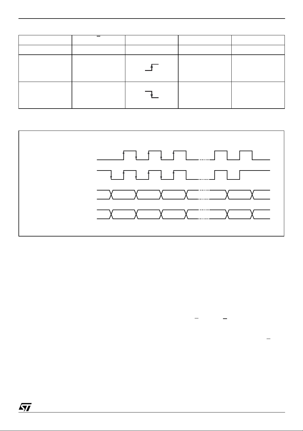
Table 2. Function Table
Mode E SCL SDI SDO
Disable Reset H Input Disabled Input Disabled High Z
M41T94
WRITE L Data Bit latch High Z
READ L X
Note: 1. SD O remains at High Z until ei ght bits of data are ready to be shifted out duri ng a READ.
AI04630
AI04631
Figure 8. Dat a and Clock Timi ng
CPOL
CPHA
0
1
0
1
C
C
SDI
SDO
MSB
MSB
Next data bit shift
LSB
LSB
AI04632
(1)
Signal Description
Serial Data Output (SDO). The output pin is
used to transfer data serially out of the Memory.
Data is shifted out on the fallin g edge of the serial
clock.
Serial Data Input (SDI). The input pin is used to
transfer data serially into t he device. Instructions,
addresses, and the data to be written, are each received this way. Input is latched on the rising edge
of the serial clock.
Serial Clock (SCL). The serial c lock provides the
timing for the serial interface (as shown in Figure
10, page 12 and Figure 11, page 12). The W/R Bit,
addresses, or data are latched, from the input pin,
on the rising edge of the clock input. The output
data on the SDO pin changes state after the falling
edge of the clock input.
The M41T94 can be d riven by a microcontroller
with its SPI periphe ral running in ei the r of the two
following modes:
(CPOL, CPHA) = ('0', '0') or
(CPOL, CPHA) = ('1', '1').
For these two modes, input data (SDI) is latched in
by the low-to-high transition of clock SCL, and output data (SDO) is shifted out on t he high-to-low
transition of SCL (see Table 2, page 7 and Figure
8, page 7).
Chip Enable (E
). When E is high, the memory
device is deselected, and the SDO output pin is
held in its high impedance state.
After power-on, a high-to-low transition on E
is re-
quired prior to the start of any operation.
7/31
Page 8
M41T94
MAXIMUM RATI N G
Stressing the device ab ove the rating listed in t he
“Absolute Maximum Ratings” table may cause
permanent damage to the device. These are
stress ratings only and operation of the dev ice at
these or any other conditions above those indicated in the Operating sections of this specification is
Table 3. Absolute Maximum Ratings
Symbol Parameter Value Unit
T
STG
Storage Temperature (VCC Off, Oscillator Off)
not implied. Exposure to Absol ute Maxim um Ra ting conditions for extended periods may affect device reliability. Refer also to the
STMicroelectronics SURE Program and other relevant quality documents.
SNAPHAT –40 to 85 °C
SOIC –55 to 125 °C
V
CC
T
SLD
V
IO
I
O
P
D
Note: 1. Ref l ow at peak t em perature of 215°C t o 225°C for < 60 seconds (total thermal budget not to exceed 180° C for betw een 90 to 120
CAUTION: Negative undershoots below –0.3V are not allowed on any pin while in the Battery Back-up mode.
CAUTION: Do NOT wave solder SOIC to avoid damaging S NA PHAT sockets.
Supply Voltage –0.3 to 7 V
(1)
Lead Solder Temperature for 10 seconds 260 °C
Input or Output Voltage
Output Current 20 mA
Power Dissipation 1 W
secon ds).
–0.3 to V
CC
+0.3
V
8/31
Page 9
DC AND AC PARAMETERS
This section summarizes the operat ing and measurement conditions, as well as the DC and AC
characteristics of the device. The parameters in
the following DC and AC Characteristic tables are
ment Conditions listed in the rel evant tables. Designers should check that the operating conditions
in their projects match the measurement conditions when using the quoted parameters.
derived from tests performed under the M easure-
Table 4. DC and AC Measurement Conditions
Parameter M41T94
V
Supply Voltage
CC
2.7 to 5.5V
Ambient Operating Temperature –40 to 85°C
Load Capacitance (C
)
L
100pF
Input Rise and Fall Times ≤ 50ns
Input Pulse Voltages
Input and Output Timing Ref. Voltages
Note: Output Hi -Z is defined as the point where dat a i s no longer dri ven.
0.2 to 0.8V
0.3 to 0.7V
Figure 9. AC Testing Input/Output Waveforms
M41T94
CC
CC
0.8V
0.2V
CC
CC
0.7V
0.3V
AI02568
CC
CC
Table 5. Capacitance
Symbol
C
IN
C
OUT
t
LP
Note: 1. Effective c apacitance measure d wi th power supply at 5V ; s am pl ed only, n ot 100% teste d.
2. At 25°C, f = 1MHz.
3. Outputs are deselect ed.
Input Capacitance 7 pF
(3)
Output Capacitance 10 pF
Low-pass filter input time constant (SDA and SCL) 50 ns
Parameter
(1,2)
Min Max Unit
9/31
Page 10
M41T94
Table 6. DC Characteristics
= 3V
CC
≤ V
≤ V
(1)
– 0.3V
CC
CC
Min Typ Max Unit
400 500 nA
0.7V
CC
2.4 V
4.20 4.40 4.50
2.55 2.60 2.70
Symb. Parameter
Battery Current OSC ON
I
BAT
Battery Current OSC OFF 50 nA
I
I
I
I
LO
V
V
V
Supply Current f = 2 MHz 2 mA
CC1
Supply Current (Standby)
CC2
(2)
Input Leakage Current
LI
(3)
Output Leakage Current
V
Input High Voltage
IH
V
Input Low Voltage –0.3
IL
Battery Voltage 2.5
BAT
OH
Output High Voltage
Output Low Voltage
OL
(4)
(4)
Output Low Voltage (Open Drain)
(5)
Test Condition
= 25°C, VCC = 0V,
T
A
V
BAT
SCL, SDI = V
0V ≤ V
IN
0V ≤ V
OUT
IOH = –1.0mA
IOL = 3.0mA
IOL = 10mA
Power Fail Deselect (THS = VCC)
V
PFD
Power Fail Deselect (THS = V
V
Note: 1. Va lid for Ambi ent Operat in g T emperat ure: TA = –40 to 85°C ; VCC = 2.7 to 5. 5V (except where note d).
Battery Back-up Switchover 2.5 V
SO
2. RSTIN1
3. Outputs Dese l ected.
4. For SQW pi n (CMOS).
5. For IRQ
6. For rechargeable ba ck-up, V
and RSTI N2 internally pulled-up t o VCC through 100KΩ resistor. WDI internally pulled-down to VSS through 100KΩ resistor.
/FT/OUT, RST pins (Ope n Drai n): i f pu ll ed- up to supp ly oth e r tha n VCC, this su ppl y mu st be equ al to, or l es s t han 3. 0V when
= 0V (durin g battery back-up mode).
V
CC
(max) may be considered VCC.
BAT
SS
)
1.4 mA
±1 µA
±1 µA
VCC + 0.3
0.3V
CC
(6)
3.5
0.4
0.4
V
V
V
V
V
Table 7. Crystal Electrical Characteristics (Externally Supplied)
Symbol
f
0
R
S
C
L
Note: 1. Load capacitors are integrated within the M41T94. Circuit board layout considerations for the 32.768 kHz crystal of minimum trace
lengths an d i solation from RF genera ting signals should be taken into acco unt. These characteristics are e xt ernally sup pl i ed.
2. STMicroelectronics recommends the KDS DT-38: 1TA/1TC252E127, Tuning Fork Type (thru-hole) or the DMX-26S:
1TJS125 F H2A212, (SM D) quartz crystal for ind u s trial temperature operations. KDS can be contacted at k ouhou@kds j .co.jp or ht tp://www.kdsj.co.jp for further information on this crystal type.
Resonant Frequency 32.768 kHz
Series Resistance 50 kΩ
Load Capacitance 12.5 pF
Parameter
10/31
(1,2)
Typ Min Max Unit
Page 11

OPERATION
The M41T94 clock operates as a slave device on
the SPI serial bus. Each memory device is accessed by a simple serial interface that is SPI bus compatible. The bus signal s are SCL, SDI and SDO
(see Table 1, page 5 and Figure 7, page 6). T he
device is selected when the Chip Enable input (E
is held low. All instructions, addresses and data
are shifted serially in and out of the chip. The most
significant bit is presented first, with the data input
(SDI) sampled on the first rising ed ge of t he clock
(SCL) after the Chip Enable (E
) goes low. The 64
bytes contained in the device can then be accessed sequentially in the following order:
1. Tenths/Hundredths of a Second Register
2. Seconds Register
3. Minutes Register
4. Century/Hours Register
5. Day Register
6. Date Register
7. Month Register
8. Year Register
9. Control Register
10. Watchdog Register
11 - 16.Alarm Registers
17 - 19.Reserved
20. Square Wave Register
21 - 64.User RAM
The M41T94 clock continually monitors V
out-of tolerance condition. Should V
V
, the device terminates an access in progress
PFD
CC
for an
CC
fall be low
and resets the device add ress counter. Inputs to
the device will not be recognized at this time to
prevent erroneous data from being written to the
device from a an out-of-tolerance system. When
falls below VSO, the device automatically
V
CC
switches over to the battery and powers down into
an ultra low current mode of operation to conserve
battery life. As system power returns and V
es above V
, the battery is disconnected, and the
SO
CC
ris-
power supply is switched t o external V
protection continues until V
plus t
(min). For more information on Battery
REC
reaches V
CC
Storage Life refer to Application Note AN1012.
SPI Bus Characteristics
)
The Serial Peripheral interface (SPI) bus is intended for synchronous communication between different ICs. It consists of four signal lines: Serial
Data Input (SDI), Serial Data Output (SDO), Serial
Clock (SCL) and a Chip Enable (E
).
By definition a device that gives out a message is
called “transmitter,” the receiving device that gets
the message is called “receiver.” The device that
controls the message is called “master.” The devices that are controlled by the master are cal led
“slaves.”
input is used to initiate and terminate a data
The E
transfer. The SCL input is used to synchronize
data transfer between the master (micro) an d the
slave (M41T94) devices.
The SCL input, which is generated by the microcontroller, is active only during address and data
transfer to any device on the SPI bus (see Figure
7, page 6).
The M41T94 can be d riven by a microcontroller
with its SPI periphe ral running in ei the r of the two
following modes:
(CPOL, CPHA) = ('0', '0') or
(CPOL, CPHA) = ('1', '1').
For these two modes, input data (SDI) is latched in
by the low-to-high transition of clock SCL, and output data (SDO) is shifted out on t he high-to-low
transition of SCL (see Table 2, page 7 and Figure
8, page 7).
There is one clock for each bit transferred. Address and data bits are transferred in groups of
eight bits. Due to m emory size the second most
significant address bit is a Don’t Care (address bit
6).
M41T94
. Write
CC
(min)
PFD
11/31
Page 12
M41T94
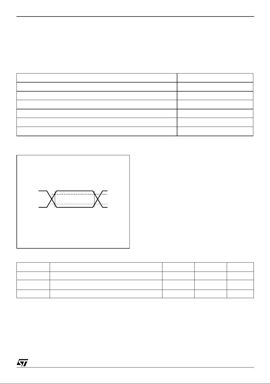
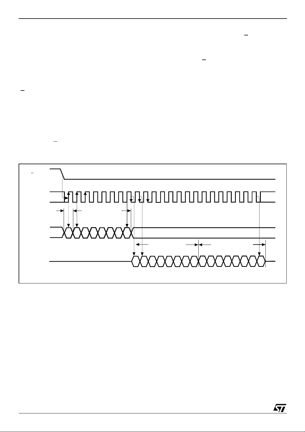
Figure 10. Input Timing Requirements
E
tELCH
SCL
tDVCH
tCHDX
tCHEH
tCLCH
tEHEL
tEHCH
tCHCL
SDI
SDO
MSB IN
HIGH IMPEDANCE
Figure 11. Output Timing Requirements
E
SCL
tCLQV
tCLQX
SDO
ADDR. LSB IN
SDI
MSB OUT
tDLDH
tDHDL
tCH
LSB IN
tCL
tQLQH
tQHQL
AI04633
tEHQZ
LSB OUT
AI04634
12/31
Page 13

Table 8. AC Characteristics
Symbol
f
SCL
(2)
t
CH
(3)
t
CHCL
t
CHDX
t
CHEH
(2)
t
CL
(3)
t
CLCH
t
CLQV
t
CLQX
(3)
t
DHDL
(3)
t
DLDH
t
DVCH
t
EHCH
t
EHEL
(3)
t
EHQZ
t
ELCH
(3)
t
QHQL
(3)
t
QLQH
Note: 1. Va lid for Ambi ent Operat in g T emperat ure: TA = –40 to 85°C ; VCC = 2.7 to 5. 5V (except where note d).
2. t
CH
3. Value guaranteed by design, not 100% tested in production.
Serial Clock Input Frequency DC 2 MHz
Clock High 200 ns
Clock Transition (Fall Time) 1 µs
Serial Clock Input High to Input Data Transition 50 ns
Serial Clock Input High to Chip Enable High 200 ns
Clock Low 200 ns
Clock Transition (Rise Time) 1 µs
Serial Clock Input Low to Output Valid 150 ns
Serial Clock Input Low to Output Data Transition 0 ns
Input Data Transition (Fall Time) 1 µs
Input Data Transition (Rise Time) 1 µs
Input Data to Serial Clock Input High 40 ns
Chip Enable High to Serial Clock Input High 200 ns
Chip Enable High to Chip Enable Low 200 ns
Chip Enable High to Output High-Z 250 ns
Chip Enable Low to Serial Clock Input High 200 ns
Output Data Transition (Fall Time) 100 ns
Output Data Transition (Rise Time) 100 ns
+ tCL ≥ 1/f
SCL
Parameter
(1)
Min Max Unit
M41T94
13/31
Page 14
M41T94
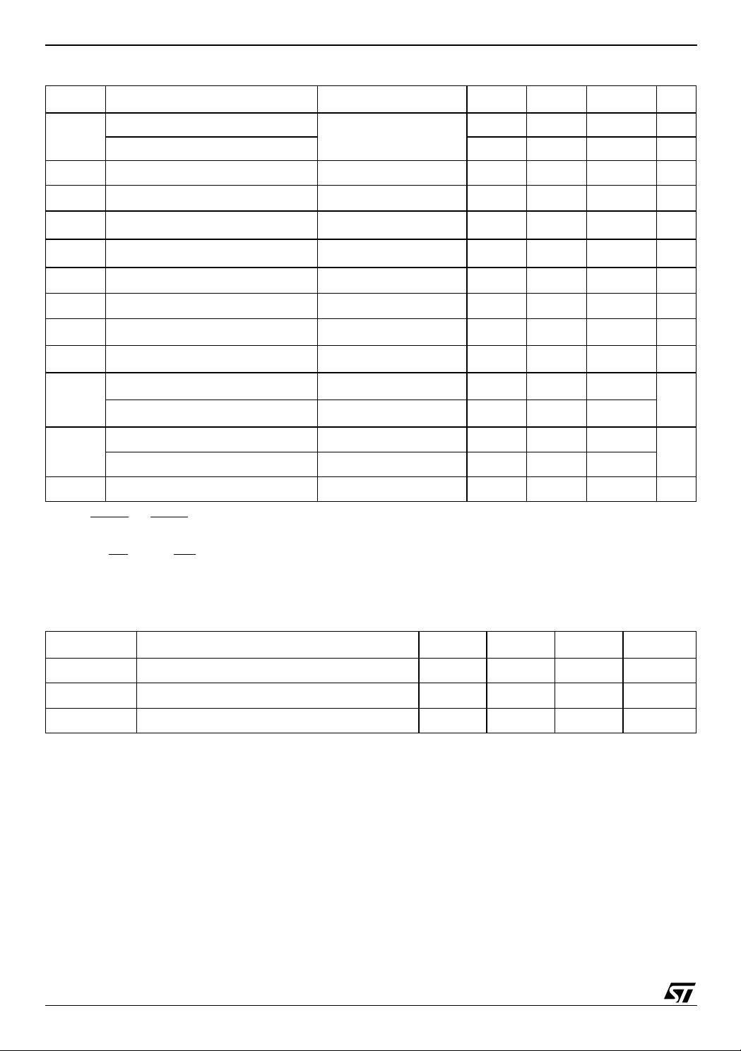
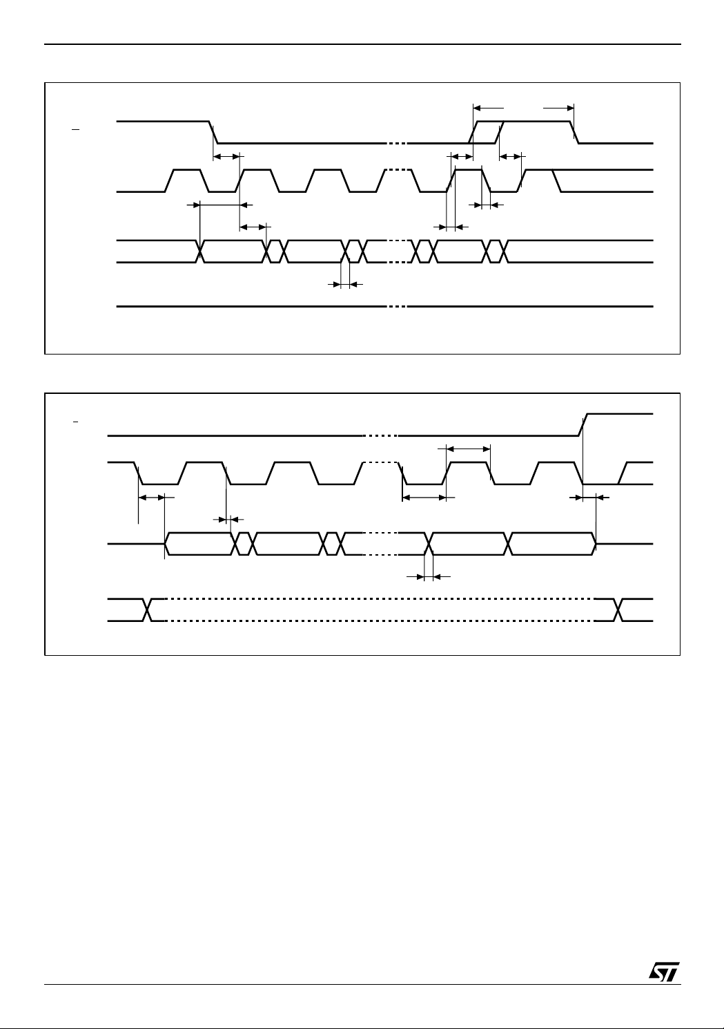
READ and WRITE Cycles
Address and data are shifted MSB first into the Serial Data Input (SDI) and out of the Serial Data
Output (SDO). Any data transfer considers the first
bit to define whether a READ or WRITE will occur.
This is followed by seven bits defini ng t he address
to be read or written. Data is transferred out of the
SDO for a READ operation and into the SDI for a
WRITE operation. The address is always the second through the eighth bit written after the Enable
) pin goes low. If the first bit is a '1,' one or more
(E
WRITE cycles will occur. If the first bit is a '0,' one
or more READ cycles will occur (see Figure 12
and Figure 13, page 15).
Data transfers can occur one byte at a time or in
multiple byte burst mode, during which the address pointer will be automatically incremented.
For a single byte transfer, one byte is read or written and then E
Figure 12. READ Mode Sequence
E
is driven high. For a multiple byte
transfer all that is required is that E
continue to remain low. Under this condition, the address pointer
will continue to increment as stated previously. Incrementin g will co ntinue until t he device is deselected by taking E
high. The addres s will wrap to
00h after incrementing to 3Fh.
The system-to-user transfer of clock data will be
halted whenever the address being read is a clock
address (00h to 07h). Although the clock continues to main tain the corr ect time, thi s will preve nt
updates of time and date during either a READ or
WRITE of these address locations by the user.
The update will resume either due to a deselect
condition or when the pointer increments to an
non-clock or RAM address (08h to 3Fh).
Note: This is true both in READ and WRITE mode.
SCL
SDI
SDO
W/R BIT
2
0
1
7 BIT ADDRESS
7
6
5
MSB
HIGH IMPEDANCE
7
7
MSB
9
8
6
5
3
4
6
3
201
4
DATA OUT
(BYTE 1)
4
5
12 13
3
201
14
15 16
17 22
6
7
MSB
DATA OUT
(BYTE 2)
4
5
3
201
AI04635
14/31
Page 15
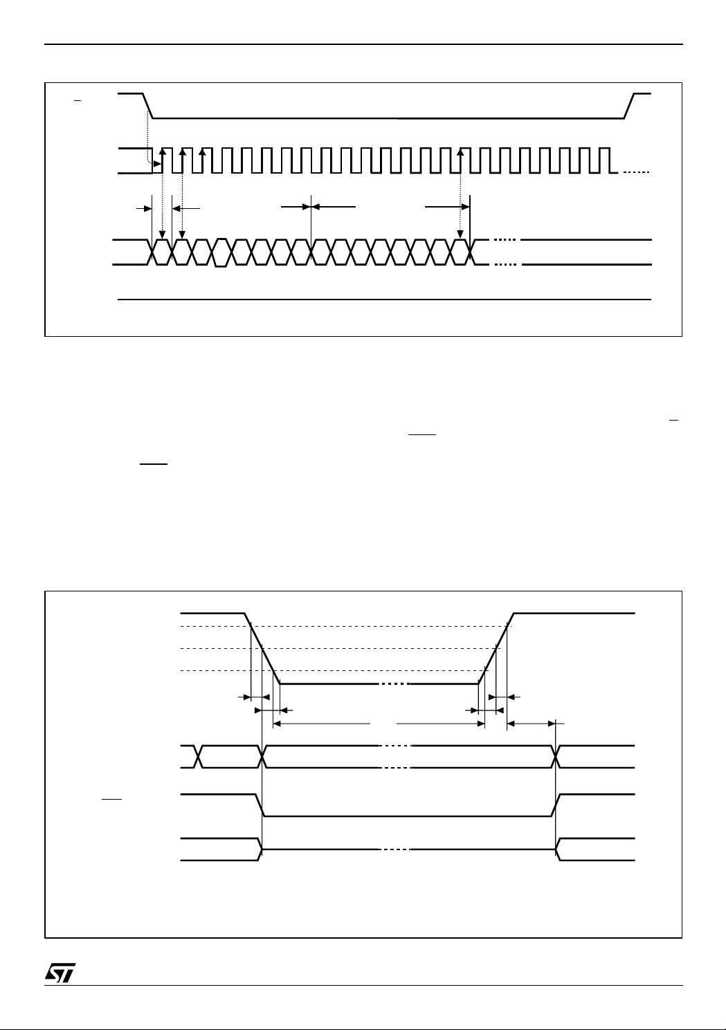
Figure 13. WRITE Mode S equence
E
M41T94
7
0
8
7
MSB
SCL
SDI
SDO
W/R BIT
7
MSB
1
2
0
7 BIT ADDR
443321
665
5
Data Retention Mode
With valid V
applied, the M41T94 can be ac-
CC
cessed as described above with REA D or WRI TE
cycles. Should the supply voltage decay, the
M41T94 will auto matic ally dese lect , wr ite pr otec ting itself when V
V
(min) (see Figure 14, pag e 15). At this time,
PFD
the R eset pin (RS T
main active until V
When V
(V
SO
falls below the switch-over voltage
CC
), power input is switched from the VCC pin to
falls between V
CC
(max) and
PFD
) is driven active and will re-
returns to nominal levels.
CC
the SNAPHAT battery (or external battery for
SO16) at this time, and the clock registers are
9
10
DATA BYTE
4321
65
HIGH IMPEDANCE
15
0
7
maintained from the attached battery supply. All
outputs become high impedance. On power up,
when V
tion continues for t
The RST
returns to a nominal value, write protec-
CC
by internally inhibiting E.
REC
signal also remains active during this
time (see Figure 14, page 15). Before the next active cycle, Chip Enable should be taken high for at
EHEL
, then lo w .
least t
For a further more detailed review of battery life-
time calculations, please see Application Note
AN1012.
AI04636
Figure 14. Power Down/Up Mode AC Waveforms
V
CC
V
(max)
PFD
V
(min)
PFD
VSO
INPUTS
RST
OUTPUTS
tF
VALID VALID
(PER CONTROL INPUT)
tFB
tDR
DON'T CARE
HIGH-Z
tRB
tR
tREC
RECOGNIZEDRECOGNIZED
(PER CONTROL INPUT)
AI03687
15/31
Page 16

M41T94
Table 9. Power Down/Up AC Characteristics
Symbol
(2)
t
F
t
FB
t
R
t
RB
t
REC
t
DR
Note: 1. Va lid for Ambi ent Operat in g T emperat ure: TA = –40 to 85°C ; VCC = 2.7 to 5. 5V (except where note d).
2. V
3. V
4. At 25°C, V
5. Programmable (see Table 14, page 23)
V
(max) to V
PFD
(3)
V
(min) to VSS VCC Fall Time
PFD
V
(min) to V
PFD
VSS to V
(5)
Power up Deselect Time 40 200 ms
Expected Data Retention Time
(max) to V
PFD
200µs after V
(min) to VSS fall time of less than tFB may cause corruption of RAM data.
PFD
= 0V (when using SOH28 + M4T2 8-BR12 S H SNAPHAT top).
CC
(min) VCC Rise Time
PFD
(min) fall time of less than tF may result in deselection/write protection not occurring until
PFD
passes V
CC
Parameter
(min) VCC Fall Time
PFD
(max) VCC Rise Time
PFD
(min).
PFD
CLOCK OPERATIONS
The eight byte clock register (s ee Table 10, p age
17) is used to both set the clock and t o read the
date and time from the clock, in a binary coded
decimal format. Tenths/Hundredths of Seconds,
Seconds, Minutes, and Hours are contained within
the first four registers. Bits D6 and D7 of Clock
Register 03h (Century/Hours Register) contain the
CENTURY ENABLE Bit (CEB) and the CENTURY
Bit (CB). Setting CEB to a '1' will cause CB to toggle, either from '0' to '1' or from '1' to '0' at the turn
of the century (depending upon its initial state). If
CEB is set to a '0,' CB will not toggle. Bits D0
through D2 of Register 04h contain the Day (day
of week). Registers 05h, 06h, and 07h contain the
Date (day of month), Month and Years. The ninth
clock register is the Control Register (this is described in the Clock Calibration section). Bit D7 of
Register 01h contains the STOP B it (ST). Set ting
this bit to a '1' will cause the oscillator to stop. If the
device is expected to s pend a significant amount
of time on the shelf, the oscillator may be stopped
to reduce current drain. When reset to a '0' the oscillator restarts within one second.
The eight Clock Registers may be read one byte at
a time, or in a sequential block. T he Cont rol Register (Address location 08h) may be accessed independently. Provision has been made to assure
that a clock update does not occur while any of the
eight clock addresses are being read. If a clock address is being read, an update of the clock regis-
(1)
Min Typ Max Unit
300 µs
10 µs
10 µs
1µs
(4)
10
ters will be halte d. This will pr event a trans ition of
data during the READ.
Note: When a power failure occurs, the Halt Update Bit (HT) will automatically be set to a '1.' This
will prevent the clock f rom u pdat ing t he clock registers, and will allow the user to read the exact time
of the power-down event. Resetting the HT Bit to
a '0' will al low th e cloc k to upd ate the c lock r egisters with the current time.
TIMEKEEPER
®
Registers
The M41T94 offers 20 internal registers which
contain Clock, Alarm, Watchdog, Flag, Square
Wave and Control data (see Table 10, page 17).
These registers are memory locations which contain external (user accessible) and internal copies
of the data (usually referred to as BiPORT
KEEPER cells). The external copies are independent of internal functions except that they are
updated periodically by the simultaneous transfer
of the incremented internal copy. The internal divider (or clock) chain will be reset upon the completion of a WRITE to any clock address.
The system-to-user transfer of clock data will be
halted whenever the clock addresses (00h to 07h)
are being written. The update will resume either
due to a deselect condition or when the pointer increments to a non-clock or RAM address.
TIMEKEEPER and Alarm Registers store data in
BCD. Control, Watchdog and Square Wave Registers store data in Binary format.
YEARS
™
TIME-
16/31
Page 17
Table 10. TIMEKEEPER® Register Map
M41T94
Addr
D7 D6 D5 D4 D3 D2 D1 D0
Function/Ra nge
BCD Format
00h 0.1 Seconds 0.01 Seconds Seconds 00-99
01h ST 10 Seconds Seconds Seconds 00-59
02h 0 10 Minutes Minutes Minutes 00-59
03h CEB CB 10 Hours Hours (24 Hour Format) Century/Hours 0-1/00-23
04h TR 0 0 0 0 Day of Week Day 01-7
05h 0 0 10 Date Date: Day of Month Date 01-31
06h 0 0 0 10M Month Month 01-12
07h 10 Years Year Year 00-99
08h OUT FT S Calibration Control
09h WDS BMB4 BMB3 BMB2 BMB1 BMB0 RB1 RB0 Watchdog
0Ah AFE SQWE ABE Al 10M Alarm Month Al Month 01-12
0Bh RPT4 RPT5 AI 10 Date Alarm Date Al Date 01-31
0Ch RPT3 HT AI 10 Hour Alarm Hour Al Hour 00-23
0Dh RPT2 Alarm 10 Minutes Alarm Minutes Al Min 00-59
0Eh RPT1 Alarm 10 Seconds Alarm Seconds Al Sec 00-59
0Fh WDF AF 0 BL 0 0 0 0 Flags
10h 0 0 0 0 0 0 0 0 Reserved
11h 0 0 0 0 0 0 0 0 Reserved
12h 0 0 0 0 0 0 0 0 Reserved
13h RS3 RS2 RS1 RS0 0 0 0 0 SQW
Keys : S = Sign Bit
FT = Frequency Test Bit
ST = Stop Bit
0 = Must be set to zero
BL = Battery Low Flag (Read only)
BMB0-BMB4 = Watchdog Multiplier Bits
CEB = Century Enable Bit
CB = Centur y B i t
OUT = Output level
AFE = Alarm Flag Enable Flag
RB0-RB 1 = Watchdog R esolution Bits
WDS = Watchdog Steeri ng Bit
ABE = Alarm in Battery Back-Up Mode Enable Bit
RPT1-RPT5 = Alarm R epeat Mode Bits
WDF = Watchdog flag (Read only)
AF = Alarm f l ag (Read only)
SQWE = Square Wave Enable
RS0-RS 3 = S Q W Frequency
HT = Halt Up date Bit
REC
Bit
TR = t
17/31
Page 18

M41T94
Setting Alarm Clock Registers
Address locations 0Ah-0Eh contain the alarm se ttings. The alarm can be configured to go off at a
prescribed time on a specific mont h, date, hour,
minute, or second, or repeat every year, month,
day, hour, minute, or second. It can al so be programmed to go off while the M41T94 is in the battery back-up to serve as a system wake-up call.
Bits RPT5-RPT1 put the alarm in the repeat mode
of operation. Table 11, p age 1 8 shows the possible configurations. Codes not listed in the table default to the once per second mode to quickly alert
the user of an incorrect alarm setting.
When the clock information matches the alarm
clock settings based on the m atch criteria d efined
by RPT5-RPT1, the AF (Alarm Flag) is set. If AFE
(Alarm Flag Enable) is also set, the alarm condition activa te s th e IR Q
/FT/OUT pin.
Note: If the address pointer is allowed to increment to the Flag Register address, an alarm condition will not cause the Interrupt/Flag to occur until
the address pointer is moved to a different ad-
Table 11. Alarm Repeat Mode
RPT5 RPT4 RPT3 RPT2 RPT1 Alarm Setting
dress. It should also be noted that if the last address written is the “Alarm Seconds,” the address
pointer will increment to the Flag address, causing
this situation to occur.
To disable the alarm, write '0' to the Alarm Dat e
Register and to RPT1–5. The IRQ
is cleared by a READ to the Flags Regist er. This
READ of the Flags Register will also reset the
Alarm Flag (D6; Register 0Fh). See Figure 15,
page 18.
The IRQ
/FT/OUT pin can also be activated in the
battery back-up mode. The IRQ
low if an alarm occurs and both ABE (Alarm in Battery Back-up Mode Enable) and A FE are set . The
ABE and AFE Bits are reset during power-up,
therefore an alarm generated during power-up will
only set AF. The user can read the Flag Register
at system boot-up to determine if an alarm was
generated while the M41T94 was in the deselect
mode during power-up. Figure 16, page 19 illustrates the back-up mode alarm timing.
/FT/OUT output
/FT/OUT will go
11111Once per Second
11110Once per Minute
11100Once per Hour
11000Once per Day
10000Once per Month
00000Once per Year
Figure 15. Alarm Interrupt Reset Waveforms
ACTIVE FLAG
IRQ/FT/OUT
0Fh0Eh 10h
HIGH-Z
AI03664
18/31
Page 19
Figure 16. Back-up Mode Alarm Waveforms
V
CC
V
PFD
V
SO
ABE, AFE Bits in Interrupt Register
AF bit in Flags Register
IRQ/FT/OUT
M41T94
tREC
HIGH-Z
Watchdog Timer
The watchdog timer can be used to detect an outof-control microprocessor. The user programs the
watchdog timer by setting the desired amount of
time-out into the Watchdog Register, address 09h.
Bits BMB4-BMB0 store a binary multiplier and the
two lower order bits RB1-RB0 select the resolution, where 00 =
1
/16 second, 01 =1/4 second,
10 = 1 second, and 11 = 4 seconds. The amount
of time-out is then determined to be the multiplication of t he five -bit m ult iplie r valu e w ith t he reso lution. (For example: writing 00001110 in the
Watchdog Register = 3*1 or 3 seconds).
Note: Accuracy of timer is within ± the selected
resolution.
If the processor does not reset the timer within the
specified period, the M41T94 sets the WDF
(Watchdog Flag) and generates a watchdog interrupt or a microprocessor reset. WDF is reset by
reading the Flags Register (0Fh).
The most significant bit of the Watchdog Register
is the Watchdog Steering Bit (WDS). When set to
a '0,' the wa tchdog will activ ate the IRQ
/FT/OUT
pin when timed-out. When WDS is set to a '1,' the
watchdog will output a negative pulse on the RS T
pin for t
. The Watchdog register and the AFE,
REC
ABE, SQWE, and FT Bits will reset to a '0' at the
HIGH-Z
AI03920
end of a Watchdog time-out when the W DS Bit is
set to a '1.'
The watchdog timer can be reset by two methods:
1. a transition (high-to-low or low-to-high) can be
applied to the Watchdog Input pin (WDI), or
2. the microprocessor can perform a WRITE of the
Watchdog Register.
The time-out period then starts over. The WDI pin
should be tied to V
if not used. In order to per-
SS
form a software reset of the watchdog timer, the
original time-out period can be written into the
Watchdog Register, effectively restarting the
count-down cycle.
Should the watchdog timer time-out, and the WDS
Bit is programmed to output an interrupt, a value of
00h needs to be written to the Watchdog Register
in order to clear the IRQ
/FT/OUT pin. This will also
disable the watchdog funct ion until i t is agai n programmed correctly. A READ of the Flags Register
will reset the Watchdog Flag (Bit D7; Register
0Fh).
The watchdog function is automatically disabled
upon power-up and the Watchdog Register is
cleared. If the watchdog function is set to output to
the IRQ
/FT/OUT pin and the Frequency Test (FT)
function is activated, the watchdog function prevails and the Frequency Test function is denied.
19/31
Page 20
M41T94
Square Wave Output
The M41T94 offers the user a programmable
square wave function which is output on the SQW
pin. RS3-RS0 bits located in 13h establish the
square wave output frequency. These frequencies
are listed in Table 12. Once the selection of the
Table 12. Square Wave Output Frequency
Square Wave Bits Square Wave
RS3 RS2 RS1 RS0 Frequency Units
0 0 0 0 None –
0 0 0 1 32.768 kHz
0 0 1 0 8.192 kHz
0 0 1 1 4.096 kHz
0 1 0 0 2.048 kHz
0 1 0 1 1.024 kHz
0 1 1 0 512 Hz
0 1 1 1 256 Hz
SQW frequency has been completed, the SQW
pin can be turned on and o ff under sof tware control with the Square Wave Enabl e Bit (SQWE) located in Register 0Ah.
1 0 0 0 128 Hz
100164Hz
101032Hz
101116Hz
11008Hz
11014Hz
11102Hz
11111Hz
20/31
Page 21
M41T94
Power-on Reset
The M41T94 continuously monitors V
falls to the power f ail detect t rip point, t he RST
V
CC
. When
CC
pulls low (open drain) and remains low on powerup for t
after VCC passes V
REC
(max). The RST
PFD
pin is an open drain output and an appropriate
pull-up resistor should be chosen to control rise
time.
Figure 17. RSTIN1
RSTIN1
RSTIN2
RST
and RSTIN2 Timing Waveform s
tRLRH1
(1)
tR1HRH tR2HRH
Reset Inputs (RSTIN1
& RSTIN2)
The M41T94 provides two independent inputs
which can generate an output reset. The duration
and function of these resets is identical to a reset
generated by a power cycle. Table 13, page 21
and Figure 17, page 21 illustrate the AC reset
characteristics of this function. Pulses shorter than
t
RLRH1
tion. RSTIN1
pulled up to V
tRLRH2
and t
will not generate a reset condi-
RLRH2
and RSTIN2 are each internally
through a 100kΩ resistor.
CC
AI03665
Table 13. Reset AC Characteristics
Symbol
(2)
t
RLRH1
(3)
t
RLRH2
(4)
t
R1HRH
(4)
t
R2HRH
Note: 1. Va lid for Ambi ent Operat in g T emperat ure: TA = –40 to 85°C ; VCC = 2.7 to 5. 5V (except where note d).
2. Pulse width less than 50ns will result in no RESET (for noise immunity).
3. Pulse width less than 20ms will result in no RESET (for noise immunity).
4. Programmable (see Table 14, page 23).
RSTIN1 Low to RSTIN1 High 200 ns
RSTIN2 Low to RSTIN2 High 100 ms
RSTIN1 High to RST High 40 200 ms
RSTIN2 High to RST High 40 200 ms
Parameter
(1)
Min Max Unit
21/31
Page 22

M41T94
Calibrating the Clock
The M41T94 is driven by a quartz-controlled oscillator with a nominal frequency of 32,768 Hz. Uncalibrated clock accuracy will not exceed ±35 PPM
(parts per million) oscillator frequency error at
25°C, which equates to abou t ±1.53 minutes per
month. When the Calibration circuit is properly employed, accuracy improves to better than +1/–2
PPM at 25°C.
The oscillation rate of crystals changes with temperature (see Figure 18, page 24). Therefore, the
M41T94 design employs periodic counter correction. The calibration circuit adds or subtracts
counts from the oscillator divider circuit at the divide by 256 stage, as shown in Figure 19, page 24.
The number of times pulses are blanked (subtracted, negative calibration) or split (added, positive
calibration) depends upon the value loaded into
the five Calibration Bits found in the Control Register. Adding counts speeds the clock up, subtracting counts slows the clock down.
The Calibration Bits occupy the five lower order
bits (D4-D0) in the Control Register (8h). T hese
bits can be set to represent any value between 0
and 31 in binary form. Bit D5 is a Sign Bit; '1' indicates positive calibration, '0' indicates negative
calibration. Calibration occurs within a 64 m inute
cycle. The first 62 m inutes i n t he c ycle m ay , onc e
per minute, have one second either shortened by
128 or lengthened by 256 oscillator cycles. If a binary '1' is loaded into the register, only the first 2
minutes in the 64 minute cycle will be modified; if
a binary 6 is loaded, t he first 12 will be affected,
and so on.
Therefore, each cal ibration step has the effect of
adding 512 or subtracting 256 oscillator cycles for
every 125,829,120 actual oscillator cycles, that is
+4.068 or –2.034 PPM of adjustm ent per calibration step in the cal ibration registe r. Ass um ing that
the oscillator is running at exactly 32,768 Hz, each
of the 31 increments in the Calibration byte would
represent +10.7 or –5.35 seconds per month
which corresponds to a total range of +5.5 or –2.75
minutes per month.
Two methods are available for ascertaining how
much calibration a given M41T94 may require.
The first involves setting the clock, letting it run for
a month and comparing it to a known accurate reference and recording deviation over a fixed period
of time. Calibration values, including the number of
seconds lost or gained in a given period, can be
found in Application Note AN934: TIMEKEEPER
CALIBRATION. This allows the designer to give
the end user the ability to calibrate the clock as the
environment requires, even if the final product is
packaged in a non-user serviceable enclosure.
The designer could provide a simple utility that accesses the Calibration Byte.
The second approach is better suit ed to a manufacturing environment, and involves the use of the
/FT/OUT pin. The pin will toggle at 512 Hz,
IRQ
when the Stop Bit (ST, D7 of 1h) is '0,' the Frequency Test Bit (FT, D6 of 8h) is '1,' the Alarm Flag
Enable Bit (AFE, D7 of Ah) is '0,' and the Watchdog Steering Bit (WDS, D7 of 9h) is '1' or the
Watchdog Register (9h = 0) is reset.
Any deviation from 512 Hz i ndicates the degree
and direction of oscillator frequency shift at the test
temperature. For example, a reading of
512.010124 Hz would indicate a +20 PPM oscillator frequency error, requiring a –10 (XX001010) to
be loaded into the Calibration Byte for correction.
Note: Setting or changing the Calibration Byte
does not affect the Frequency Test output frequency.
The IRQ
/FT/OUT pin is an open drain output
which requires a pull-up resistor for proper operation. A 500 to 10kΩ resistor is recommended in order to control the rise time. The F T Bit is cleared
on power-down.
Century Bit
Bits D7 and D6 of Clock Register 03h contain the
CENTURY ENABLE Bit (CEB) and the CENTURY
Bit (CB). Setting CEB to a '1' will cause CB to toggle, either from a '0' to '1' or from '1' to '0' at the turn
of the century (depending upon its initial state). If
CEB is set to a '0,' CB will not toggle.
Output Driver Pin
When the FT Bit, AFE Bit and Wat chdog Regi ster
are not set, the IRQ
/FT/OUT pin becomes an output driver that reflects the contents of D7 of the
Control Register. In other words, when D7 (OUT
Bit) and D6 (FT Bit) of address location 08h are a
'0,' then the IRQ
Note: The IRQ
/FT/OUT p in w ill be dr iv en lo w .
/FT/OUT pin is an open drain which
requires an external pull-up resistor.
22/31
Page 23

Battery Low Warning
The M41T94 automatically performs battery voltage monitoring upon power-up and at factory-programmed time intervals of approximately 24
hours. The Battery Low (BL) Bit, Bit D4 of Flags
Register 0Fh, will be asserted if the battery voltage
is found to b e less than approximately 2.5V. T he
BL Bit will remain asserted until completion of battery replacement and subsequent battery low
monitoring tests, either during the nex t power-up
sequence or the next scheduled 24-hour interval.
If a battery low is generated during a power-up sequence, this indicates that the battery is below approximately 2.5 volts and may not be able to
maintain data integrity in the SRAM. Data shou ld
be considered suspect an d verified as correct. A
fresh battery should be installed.
If a battery low indication is generated during the
24-hour interval check, this indicates that the battery is near end of life. However, data is not compromised due to the fact that a nominal V
CC
is
supplied. In order to insure data integrity during
subsequent periods of bat tery back-up m ode, the
battery should be replaced. The SNAPHAT top
may be replaced while V
is applied to the de-
CC
vice .
M41T94
Note: This will cause the clock to lose time during
the interval the SNAPHAT battery/crystal top is
disconnected.
The M41T94 only monitors the battery when a
nominal V
cations which require extensive durations in the
battery back-up mode should be powered-up periodically (at least once every few months) in order
for this technique to be beneficial. Additionally, if a
battery low is indicated, data integrity should be
verified upon power-up via a checksum or other
technique.
Bit
t
REC
Bit D7 of Clock Register 04h contains the t
(TR). t
the deselect time aft er V
lows for a voltage setting time before WRITEs may
again be performed to the device after a powerdown condition. The t
set the length of t his deselect tim e as defined by
Table 14.
Initial Power-on Defaults
Upon initial application of power to the device, the
following register bits are set to a '0' state: Watchdog Register, TR, FT, AFE, ABE, and SQWE. The
following bits are set to a '1' state: ST, OU T, and
HT (see Table 15).
is applied to the device. Thus appli-
CC
refers to the automatic continuation of
REC
reaches V
CC
Bit will allow the user to
REC
PFD
Bit
REC
. This al -
Table 14. t
t
REC
Note: 1. Def ault Sett i ng
Definitions
REC
Bit (TR)
0 0 96 98 ms
0140
1 X 50 2000 µs
Table 15. Default Values
Condition TR ST HT Out FT AFE ABE SQWE
Initial Power-up
(Battery Attach for SNAPHAT)
Subsequent Power-up (with
battery back-up)
Note: 1. BMB0-BMB4, RB0, RB1.
2. State of other contro l b its undefined.
3. UC = Unchanged
(3)
t
Time
STOP Bit (ST)
01110000 0
(2)
UC UC 1 UC 0 0 0 0 0
Min Max
REC
200
(1)
Units
ms
WATCHDOG
Register
(1)
23/31
Page 24
M41T94
Figure 18. Crystal Accuracy Across Temp eratur e
Frequency (ppm)
20
0
–20
–40
–60
–80
–100
–120
–140
–160
0 10203040506070
∆F
F
Temperature °C
= -0.038 (T - T
ppm
2
C
T0 = 25 °C
)2 ± 10%
0
80–10–20–30–40
AI00999
Figure 19. Cal ib rat i on Waveform
NORMAL
POSITIVE
CALIBRATION
NEGATIVE
CALIBRATION
AI00594B
24/31
Page 25
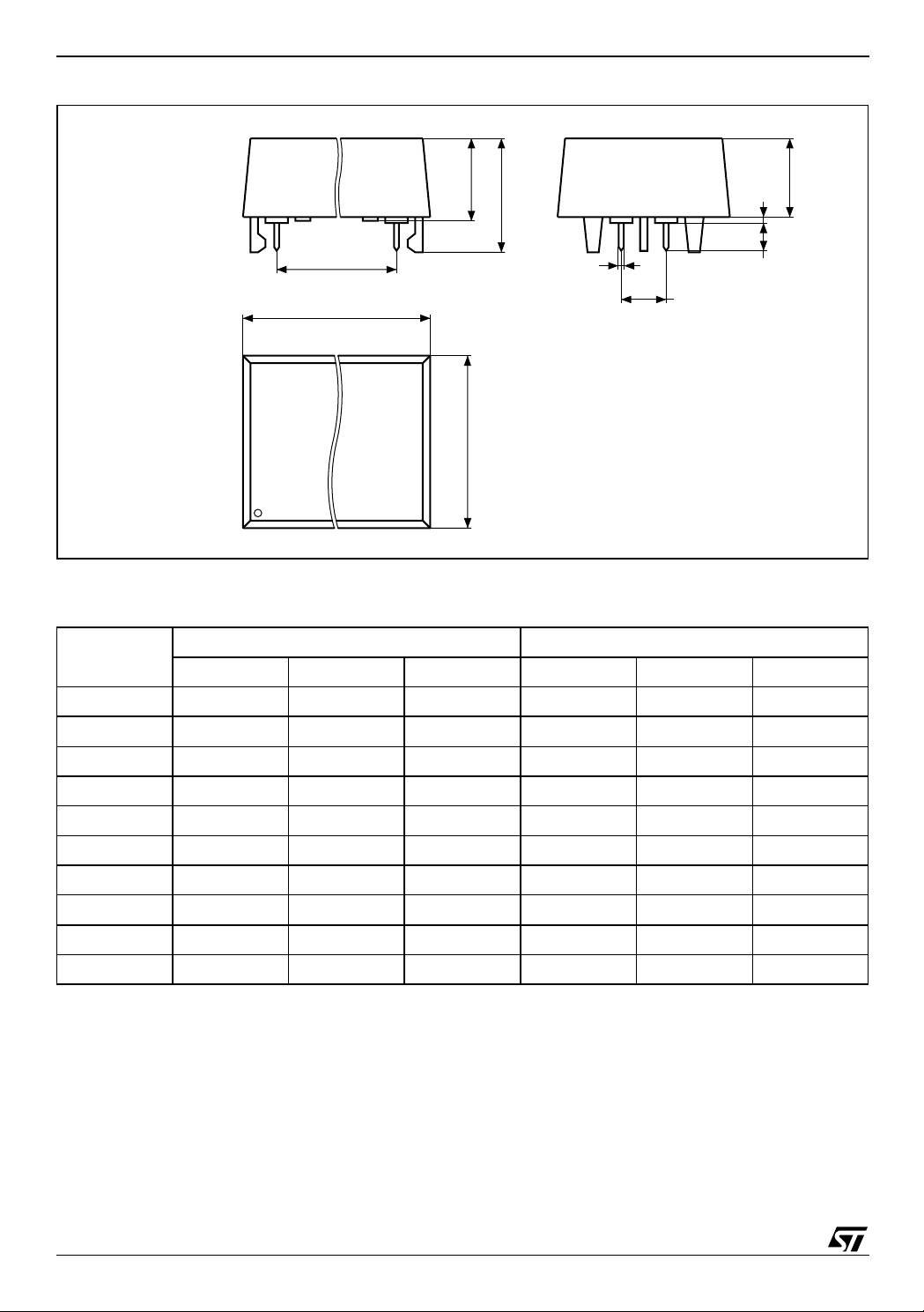
PACKAGE MECHANICAL INFORMATION
Figure 20. SO16 – 16-lead Plastic Small Outline Pac kage Ou tline
M41T94
A2
A
B
e
CP
D
N
E
H
1
SO-b
Note: Drawing is not to scale.
Table 16. SO16 – 16-lead Plastic Small Outline Packag e Mec han ical Data
Symbol
Typ. Min. Max. Typ. Min. Max.
A – – 1.75 – – 0.069
A1 – 0.10 0.25 – 0.004 0.010
millimeters inches
C
LA1 α
A2 – – 1.60 – – 0.063
B – 0.35 0.46 – 0.014 0.018
C – 0.19 0.25 – 0.0 07 0.010
D – 9.80 10.00 – 0.386 0.394
E – 3.80 4.00 – 0.150 0.158
e 1.27 – – 0.050 – –
H – 5.80 6.20 – 0.2 28 0.244
L – 0.40 1.27 – 0.016 0.050
a – 0° 8° – 0° 8°
N16 16
CP – – 0.10 – – 0.0 04
25/31
Page 26

M41T94
Figure 21. SOH28 – 28-lead Plastic Small Outline, Battery SNAPHAT, Package Outline
A2
A
C
Be
eB
CP
D
N
E
H
LA1 α
1
SOH-A
Note: Drawing is not to scale.
Table 17. SOH28 – 28-lead Plastic Small Outline, battery SNAPHAT, Package Mecha nical Data
Symbol
Typ Min Max Typ Min Max
millimeters inches
A – – 3.05 – – 0.120
A1 – 0.05 0.36 – 0.002 0.014
A2 – 2.34 2.69 – 0.092 0.106
B – 0.36 0.51 – 0.014 0 .020
C – 0.15 0.32 – 0.006 0.012
D – 17.71 18.49 – 0. 697 0.728
E – 8.23 8.89 – 0.324 0 .350
e 1.27 – – 0.0 50 – –
eB – 3.20 3.61 – 0.126 0.142
H – 11.51 12.70 – 0.453 0.500
L – 0.41 1.2 7 – 0.016 0.050
α –0°8°–0°8°
N 28 28
CP – – 0.10 – – 0.004
26/31
Page 27

Figure 22. SH – 4-pin SNAPHAT Housing for 48mAh Battery & Crystal, Package Outline
M41T94
A2
A3
L
eA
D
A1
A
B
eB
E
SHTK-A
Note: Drawing is not to scale.
Table 18. SH – 4-pin SN AP HAT Housing for 48mAh B atter y & Crystal, Package Mechanical Data
Symbol
T yp Min Max Typ Min Max
A – – 9.78 – – 0.385
millimeters inches
A1 – 6.73 7.24 – 0.265 0.285
A2 – 6.48 6.99 – 0.255 0.275
A3 – – 0.38 – – 0.015
B – 0.46 0.56 – 0.018 0.022
D – 21.21 21.84 – 0.835 0.8560
E – 14.22 14.99 – 0.556 0.590
eA – 15.55 15.95 – 0.612 0.628
eB – 3.20 3.61 – 0.126 0.142
L – 2.03 2.29 – 0.080 0.090
27/31
Page 28
M41T94
Figure 23. SH – 4-pin SNAPHAT Housin g f or 120mAh Battery & Crystal, Package Outline
A2
A3
L
eA
D
A1
A
B
eB
E
SHTK-A
Note: Drawing is not to scale.
Table 19. SH – 4-pin SNAPHAT Housing f o r 120mAh Bat tery & Cryst al, Package Mechanical Data
Symbol
T yp Min Max Typ Min Max
A – – 10.54 – – 0.415
A1 – 8.00 8.51 – 0.315 0.335
millimeters inches
A2 – 7.24 8.00 – 0.285 0.315
A3 – – 0.38 – – 0.015
B – 0.46 0.56 – 0.018 0.022
D – 21.21 21.84 – 0.835 0.860
E – 17.27 18.03 – 0.680 0.710
eA – 15.55 15.95 – 0.612 0.628
eB – 3.20 3.61 – 0.126 0.142
L – 2.03 2.29 – 0.080 0.090
28/31
Page 29
M41T94
PART NUMBERING
Table 20. Ordering Information Scheme
Example: M41T 94 MH 6 TR
Device Type
M41T
Supply Voltage and Write Protect Voltage
94 = V
= 2.7 to 5.5V
CC
THS = V
THS = V
; 4.20V ≤ V
CC
; 2.55V ≤ V
SS
PFD
PFD
≤ 4.50V
≤ 2.70V
Package
MQ = SO16
(1)
MH
= SOH28
Temperature Rang e
6 = –40 to 85°C
Shipping Method for SOIC
blank = Tubes
TR = Tape & Reel
Note: 1. T he 28-pin SO I C package (S OH28) re quires the battery/c rystal package (SNAPHAT®) which is ordered separately under the part
number “M 4T XX-BR12S HX” in plas tic tube or “M4T X X-BR12 SH XTR” in Tape & Reel form .
Caution: Do NOT place the SNAPHAT bat tery package “ M4TXX-BR12SH” in c onductive foam a s it will drain th e lithiu m but ton-cell
battery.
For a list of available options (e.g., Speed, Package) or for further information on any aspect of this device,
please contact the ST Sales Office nearest to you.
Table 21. SNAPHAT Battery Table
Part Number Description Package
M4T28-BR12SH Lithium Battery (48mAh) and Crystal SNAPHAT SH
M4T32-BR12SH Lithium Battery (120mAh) and Crystal SNAPHAT SH
29/31
Page 30

M41T94
REVISION HIST ORY
Table 22. Document Revision History
Date Rev. # Revision Details
April 2002 1.0 First edition
25-Apr-02 1.1 Adjust graphic (Figure 6); fix table text (Table 3, 20); adjust characteristics (Table 6. 7)
03-Jul-02 1.2
06-Nov-02 1.3 Correct dimensions (Table 19)
26-Mar-03 1.4 Update test condition (Table 9)
28-Apr-03 2.0 New Si changes (Figure 6;Table 9, 13, 14, 15)
Modify DC, Crystal Electrical Characteristics footnotes, Default Value table (Tables 6,
7, 15)
30/31
Page 31

M41T94
Information furnished is believed to be accurate and reliable. However, STM ic roelectronics assu m es no responsibility for the consequences
of use of such information nor for any infringement of patents or other rights of third parties which may result from its use. No license is granted
by implic ation or o th erwise under any patent or patent rights of STMi croelectronics. Sp ecifications menti oned in thi s publicati on are subject
to change without notice. This publication supersedes and replaces all information previously supplied. STMicroelectronics produ ct s are not
authorized for use as cri tical comp onents in lif e support dev i ces or systems wi thout exp ress written approval of STMicroel ectronics.
The ST log o i s registered trademark of STMicroelectronics
All other names are the property of their respective ow ners.
© 2003 STMicroelectronics - All Rights Reserved
STMicroelectron ics GROUP OF COMPANIES
Australi a - Brazil - Canada - China - Finland - F rance - Germ any - Hong Ko ng - India - Israel - Italy - Ja pan - Malaysia -
Malta - Mor occo - Singapore - Spain - Sweden - S witzerlan d - United Kingdom - U.S. A.
www.st.com
31/31
 Loading...