

Page 1

User’s Manual
Model SR844
RF Lock-In Amplifier
email: infor@thinkSRS.com • www.thinkSRS.com
1290-D Reamwood Avenue
Sunnyvale, California 94089
Phone: (408) 744-9040 • Fax: (408) 744-9049
Copyright © 1997, 2007, 2013 by SRS, Inc.
All Rights Reserved.
Revision 2.9 (07/2016)
Page 2

Certification
Stanford Research Systems certifies that this product met its published specifications at the
time of shipment. Stanford Research Systems further certifies that its calibration
measurements are traceable to the United States National Institute of Standards and
Technology (NIST).
Warranty
This Stanford Research Systems product is warranted against defects in materials and
workmanship for a period of one (1) year from the date of shipment.
Service
For warranty service or repair, this product must be returned to a Stanford Research
Systems authorized service facility. Contact Stanford Research Systems or an authorized
representative before returning this product for repair.
Information in this document is subject to change without notice.
Copyright © Stanford Research Systems, Inc., 1997, 2007, 2013, 2016. All rights reserved.
Stanford Research Systems, Inc.
1290-D Reamwood Avenue
Sunnyvale, California 94089
Printed in U.S.A.
SR844 RF Lock-In Amplifier
Page 3

i
Safety and Preparation For Use
WARNING! Dangerous voltages, capable of causing injury or death, are present in this
instrument. Use extreme caution whenever the instrument cover is
removed. Do not remove the cover while the unit is plugged into a live
outlet.
Caution This instrument may be damaged if operated with the LINE VOLTAGE SELECTOR set
for the wrong AC line voltage or if the wrong fuse is installed.
Line Voltage The SR844 operates from a 100V, 120V, 220V, or 240V nominal AC power source
Selection having a line frequency of 50 or 60 Hz. Before connecting the power cord to a power
source, verify that the LINE VOLTAGE SELECTOR card, located in the rear panel fuse
holder, is set so that the correct AC input voltage value is visible.
Conversion to other AC input voltages requires a change in the fuse holder voltage card
position and fuse value. Disconnect the power cord, open the fuse holder cover door and
pull the fuse-pull lever to remove the fuse. Remove the small printed circuit board and
select the operating voltage by orienting the printed circuit board so that the desired
voltage is visible when the circuit board is pushed firmly into its slot. Push the fuse-pull
lever back into its normal position and insert the correct fuse into the fuse holder.
Line Fuse Verify that the correct line fuse is installed before connecting the line cord. For
100V/120V, use a 1 Amp fuse and for 220V/240V, use a 1/2 Amp fuse.
Line Cord The SR844 has a detachable, three-wire power cord for connection to the power source
and to a protective ground. The exposed metal parts of the instrument are connected to
the outlet ground to protect against electrical shock. Always use an outlet which has a
properly connected protective ground.
Service Do not attempt to service or adjust this instrument unless another person, capable of
providing first aid or resuscitation, is present.
Do not install substitute parts or perform any unauthorized modifications to this
instrument. Contact the factory for instructions on how to return the instrument for
authorized service and adjustment.
Fan The fans in the SR844 are required to maintain proper operation. Do not block the vents
in the chassis or the unit may not operate properly.
Warning! Regarding Use With Photomultipliers and Other Detectors
The front end amplifier of this instrument is easily damaged if a photomultiplier is used
improperly with the amplifier. When left completely unterminated, a cable connected to a
PMT can charge to several hundred volts in a relatively short time. If this cable is
connected to the inputs of the SR844 the stored charge may damage the front-end op
ampls. To avoid this problem, always connect the PMT output to the SR844 input before
turning the PMT on.
SR844 RF Lock-In Amplifier
Page 4
ii
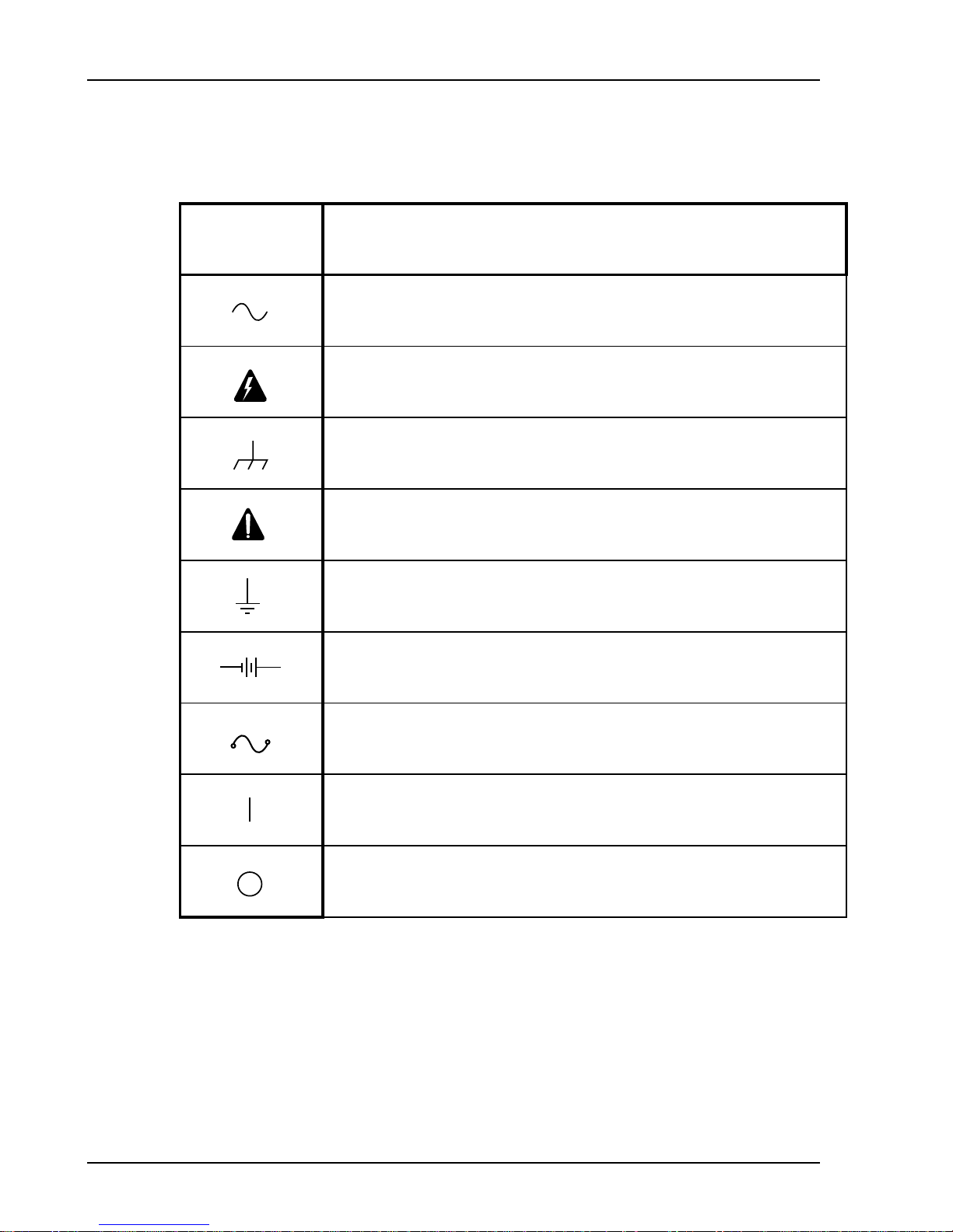
Symbols that may be found on SRS products
Symbol Description
Alternating current
Caution - risk of electric shock
Frame or chassis terminal
Caution - refer to accompanying documents
Earth (ground) terminal
Battery
Fuse
On (supply)
Off (supply)
SR844 RF Lock-In Amplifier
Page 5

iii
Contents
General Information
Safety and Preparation For Use i
Contents iii
Specifications v
Chapter 1 Getting Started
Quick Start 1-3
The Basic Lock-In 1-5
X, Y, R,
Outputs, Offsets and Expands 1-12
Storing and Recalling Setups 1-18
Aux Outputs and Inputs 1-19
Chapter 2 SR844 Basics
What is a Lock-In Amplifier? 2-3
The Functional SR844 2-8
RF Signal Input Path 2-9
Reference Channel 2-10
I.F. Section 2-11
Inside the DSP 2-12
Analog Outputs and Scaling 2-15
What is Dynamic Reserve ? 2-17
Sources of Error 2-19
Using the SR844 as a Double Lock-In 2-22
Noise Measurements 2-23
Intrinsic (Random) Noise Sources 2-24
External Noise Sources 2-25
θ and dBm 1-9
Chapter 3 Operation
Overview 3-3
Signal Input 3-8
Time Constants 3-11
Sensitivity 3-13
CH1 Display and Output 3-15
CH2 Display and Output 3-20
Reference Section 3-26
Save and Recall 3-30
Interface 3-31
Scan and Rel 3-33
Auto Functions 3-40
Shift Functions 3-41
SR844 RF Lock-In Amplifier
Page 6

iv Contents
Chapter 4 Programming
Index of Commands 4-2
Introduction 4-7
Command Syntax 4-10
Status Register Definitions 4-31
Example Program 4-34
Chapter 5 Testing
Getting Ready 5-3
Self Test 5-5
Amplitude Response 5-7
Phase Response 5-9
Frequency Accuracy 5-11
Ref Out Amplitude 5-13
DC Outputs and Inputs 5-15
Input Noise 5-17
SR844 Performance Test Record 5-19
Chapter 6 Circuitry
Service 6-3
Circuit Board Locations 6-4
Circuit Descriptions 6-6
Parts Lists 6-25
Schematic Diagrams 6-80
SR844 RF Lock-In Amplifier
Page 7
v
Specifications
Specifications apply after 30 minutes of warm-up. All specifications are with output filtering enabled (6,
12, 18 or 24 dB/oct) and 2F detection OFF, unless stated otherwise.
Signal Input
Voltage Input single-ended BNC.
Input Impedance 50 Ω or 1 MΩ || 30 pF.
Damage Threshold ±5 V (DC+AC)
Bandwidth 25 kHz to 200 MHz.
Full Scale Sensitivity 100 nV to 1V rms in a 1-3-10 sequence.
Gain Accuracy
< 50 MHz ±0.25 dB
< 200 MHz ±0.50 dB
Gain Stability 0.2%/°C
Coherent Pickup Low Noise Wide Reserve, Sensitivity < 30 mV.
f < 10 MHz < 100 nV (typical)
f < 50 MHz < 2.5 µV (typical)
f < 200 MHz < 25 µV (typical)
Input Noise: 50 Ω Input
100 kHz < f < 100 MHz 2 nV/√Hz (typical), < 4 nV/√Hz (max).
25 kHz < f < 200 MHz < 5 nV/√Hz (typical), < 8 nV/√Hz (max).
Input Noise: 1 MΩ Input
25 kHz < f < 200 MHz 5 nV/√Hz (typical), < 8 nV/√Hz (max).
Dynamic Reserve > 60 dB (expand off)
Reference
External Reference Input 25 kHz to 200 MHz.
Impedance 50 Ω or 10 kΩ || 40 pF.
Level 0.7 Vpp digital or 0 dBm sinusoidal signal.
Pulse Width > 2 ns at any frequency.
Threshold Setting Automatic, set to midpoint of waveform extrema.
Acquisition Time < 10 s (auto-ranging, any frequency).
< 1 s (within same octave).
Internal Reference Oscillator 25 kHz to 200 MHz.
Frequency Resolution 3 digits.
Frequency Accuracy ±0.1 in the 3rd digit.
Phase Noise -90 dBc/Hz at f=100 MHz, ∆f=100 Hz.
Reference Outputs Phase locked to either Internal or External reference.
Front Panel Ref Out 25 kHz to 200 MHz square wave, 1.0 Vpp nominal into 50 Ω.
Rear Panel TTL Out
Harmonic Detect
Phase Resolution 0.02°
Absolute Phase Error
< 50 MHz < 2.5°
< 100 MHz < 5.0°
< 200 MHz < 10.0°
25 kHz to 1.5 MHz, 0 to +5 V nominal, ≥ 3 V into 50
Detect at 50 kHz
≤ 2×Reference ≤ 200 MHz.
Ω.
SR844 RF Lock-In Amplifier
Page 8
vi Specifications
Reference
Relative Phase Error,
Orthogonality
Phase Noise 0.005° rms at 100 MHz, 100 ms time constant.
Phase Drift
< 10 MHz < 0.1°/°C
< 100 MHz < 0.25°/°C
< 200 MHz < 0.5°/°C
< 2.5°
Demodulator
Zero Stability Digital displays have no zero drift.
Analog outputs have < 5ppm/
Filtering
Time Constants 100 µs to 30 ks with 6, 12, 18 or 24 dB/octave roll-off.
None 10 to 20 µs update rate (X and Y outputs), 60 µs (R and θ outputs).
Harmonic Rejection
Odd Harmonics
Other Harmonics and
Sub-harmonics
Spurious Responses
-10 dBc @ 3×Ref, -14 dBc @ 5×Ref, etc.
< -40 dBc
-10 dBc @ Ref ± 2×IF
-23 dBc @ Ref ± 4×IF
< -30 dBc otherwise.
°C drift for all dynamic reserve settings.
Displays
Channel 1 Channel 2 Reference
Type 4½ digit LED 4½ digit LED 4½ digit LED
Displayed X Y Reference Frequency
Quantities R [Volts] θ [degrees] Reference Phase
R [dBm] Y-noise [Volts] Aux Output Voltages
X-noise Y-noise [dBm] Offsets in % of Full Scale
AUX IN 1 AUX IN 2 IF Frequency
Elapsed Settling Time
Ratio The signal may be ratioed with respect to AUX IN 1 or
2. The ratio is applied to both X and Y before
computation of R, R[dBm], X-noise, Y-noise [V, dBm]
and so affects all of these quantities. The ratio input is
normalized to 1 V and has a dynamic range > 100.
Expand The CH1 and CH2 displays and outputs may be
expanded by ×10 or ×100.
SR844 RF Lock-In Amplifier
Page 9
Specifications vii
CH1 and CH2 Outputs
Connectors
Front Panel BNC.
Voltage Range
10V full scale proportional to X, Y or CH1, CH2 displayed quantity.
±11V full scale for phase
Update Rate
X, Y
48 to 96 kHz
R, θ, Aux Inputs
12 to 24 kHz
X Noise, Y Noise
512 Hz
Aux Inputs and Outputs
Connectors
Rear Panel BNC.
Inputs
2
Type
Range
Differential with 1 MΩ input impedance on both signal and shield.
±10V
Resolution
1/3 mV
Bandwidth
3 kHz
Outputs
2
Range
±10V
Resolution
1 mV
Environmental Conditions
Operating
Temperature: +10°C to +40°C
Relative Humidity: <90% Non-condensing
Non-Operating
Temperature: –25°C to +65°C
Relative Humidity: <95% Non-condensing
General
Furnished Accessories
Power Cord
Operating Manual
Interfaces
IEEE-488.2 and RS232 interfaces standard. All instrument functions
can be controlled and read through either interface.
Power
70 Watts, 100/120/220/240 VAC, 50/60 Hz.
Dimensions
17" W x 5.25" H x 19.5" D
Weight
23 lb.
Warranty
One year parts and labor on materials and workmanship.
±
(Specifications apply over +18°C to +28°C)
SR844 RF Lock-In Amplifier
Page 10

viii
SR844 RF Lock-In Amplifier
Page 11

1-1
Chapter 1
Getting Started
The tutorials in this chapter are designed to acquaint the first time user with the SR844 RF Lock-In
Amplifier. The functions and features of the SR844 are grouped together into several short tutorials. You
may choose to do the tutorials selectively depending on your level of experience and your measurement
needs. Do not be concerned that your measurements do not agree exactly with the printed values in the
manual; the focus of these exercises is to learn how to use the instrument.
For all of the tutorials it is expected that you have installed the instrument with the line voltage setting
appropriate to the AC power available. If you have not done so, please see the section Line Voltage
Selection under Safety and Prepar ation for Use (page i) before proceeding further.
The experimental procedures are detailed in two columns. The left column lists the actual steps to be
performed. The right column is an explanation of each step. The front panel Keys, Knob and
READOUTS are denoted in special fonts. Indicators are shown in Bold and connectors in CAPITALS.
In This Chapter
Quick Start 1-3
The Basic Lock-In 1-5
X, Y, R, θθθθ and dBm 1-9
Output s, Off set s and Expands 1-12
Storing and Recalling Setups 1-18
Aux Outputs and Inputs 1-19
SR844 RF Lock-In Amplifier
Page 12

1-2 G et t ing Start ed
SR844 RF Lock-In Amplifier
Page 13

Quick S t art 1-3
Quick Start
This section will lead you through the most basic se tup and use of the SR844 RF lock-in amplifier. You
must have selected the line voltage (page i) and connected AC power in order to proceed further.
For this section you will need one BNC cable .
1 D isc onnect all cables from the SR844. Check
that the power cord is connected.
2 Turn the power on while holding down the
Setup key.
3 Wait until the power-on tests a re c ompleted. The instrument first displays SR844 followed by
4 If any of the tests FAIL, try power-on once
more with the Setup button held d own. If the
test FAILs again, note the ROM version and
Serial Number and contact either the factory
or your local representative.
If the Setup key is pressed during power-on, the
instrument perfo rms po wer-on te s t s a nd re tu rns to
its factory preset settings.
the unit’s serial number (CH1 and CH2 displays)
and the firmware revision number (Reference
display).
Several tes ts a re p erformed after this. T he message
DATA TEST PASS follows a read/write test to
the processor RAM. BATT TEST PASS refers to
a test of the battery-backed-up memory. PROG
TEST PASS follows a test of the instrument
program ROM. DSP T EST PASS refers to the
Digital Signal Processor (DSP). RCAL STD SET
is shorthand for Recall Standard Setup (factory
defaults). N ormally, the Setup button is not pressed
during power-up and the last message will instead
be RCAL USER SET , which means that the
previous User’s setup has been recalled.
5 Connect REF OUT on the front panel to the
SIGNAL IN with the BNC cable.
The SR844 defaults to the internal oscillator set at
1.00 MHz. T he reference mode is indicated by the
INTERNAL LED. In this mode the SR844
generates a reference signal at the selected
frequency and de tects input signals in phase and in
quadrature with this reference. A 1. 0 Vpp square
wave reference signal is available at REF OUT.
SR844 RF Lock-In Amplifier
Page 14

1-4 Quick Start
At 1 MHz, a quarter wavelength is roughly 50
6
Check the readings on the front panel
Press CH1 Display to select R [dBm]. The R[dBm]
meters of BNC cable. Your BNC cable is probably
a lot shorter than this, so the signal input is close to
being in phase with the reference.
displays.
display on CH1 should read +5.6 to +9.6 dBm.
SR844 RF Lock-In Amplifier
Page 15

Th e Basic Lock-I n 1-5
The Basic Lock-In
This measurement is designed to use the interna l os c illa tor to e xplore some of the basic loc k-in
operations. Yo u s hould alrea dy be familiar with the fund amentals of lock-in detection. See C hapter 2 for a
discuss ion of the bas ics of lock-in me as urements.
Specifically, you will measure the amplitude of the reference oscillator at various frequencies,
sensitivities , time constants and phases. You will need a BNC ca ble for this sec tion.
1 D isc onnect all cables from the SR844.
If the power is off, turn it on. Wait for selftests to c omplete.
2 Press Shift then Recall (PRESET) to restore
factory presets.
3 Connect REF OUT on the front pa nel to the
SIGNAL IN with the BNC cable.
Turn on the unit.
We will start with the unit in its factory pres e t
configuration.
The factory preset configuration is Internal
Refere nce mode (shown by the INTERNAL LED)
at 1.00 MHz, shown on the Reference display.
The time constant is 100 ms (shown by the time
constant indicators 1, ××××100 and ms above the Time
Constant Up/Do wn keys) and the sensitivity is 1 V
rms (the indicators a re b elo w the Sensitivity
Up/Down keys).
The SR844 reference output (1.0 Vpp nominal
square wave into 50
measurement range (1 Vrms) so we can connect it
directly to the input. The SR844 input impedance is
set to 50 Ω
appropriate for the REF OUT.
(shown by the 50
Ω
) is within the unit’s
ΩΩΩΩ
indicator) which is
The BNC cable has a small phase shift at 1 MHz
(the free-space wavelength is 300 m), so the input
signal should be mostly X (in-phase) with a small Y
(quadrature) component.
The CH1 Display is set to X and should s how
something close to 0.54 V. The CH2 display is set
to Y and should show le s s than
±
0.05 V.
SR844 RF Lock-In Amplifier
Page 16

1-6 T he Basic Lock-In
Reme mber, the s ignal is a 0.5 Vpk (1.0 Vpp) s qua re
wave. A square wave is composed of signa ls at all
odd harmonics. The SR844 is a square wave
detecting lock-in and detects all of the odd
harmonics of the fundamental. T he amplitude of the
fundame ntal (at 1. 00 MHz) is 4/
π
x Vpk. The
contribution from all odd harmonics is
1 + (1/3)2 + (1/5)2 + (1/7)2 + ... ≈ 1.19
The detected amplitude is 4/
π
x 0.5 Vpk x 1. 19 or
0.759 Vpk. The SR844 reads the s ignal in units of
Vrms (0.707 x Vpk) or 0.537 Vrms .
The CH1 display may not read exa ctly 0. 54 V for a
number of reasons:
• The REF OUT amplitude is only a nominal
specification.
• The basic accuracy of the unit is
±
0.25 dB
(3%).
• Since the phase may not be exactly 0
°
, X=Rcos
is slightly less than R (amplitude ).
4 Press Shift then Phase to perform
AutoPhase.
This adjusts the reference phase inside the
instrument. (The phase at which the signal is
detected changes, but Ref Out remains unchanged.)
This should set the value of Y (on the C H2 display)
to zero.
5 Press Phase. Display the reference phas e. It should be close to
zero.
θ
6
Press the +90° key.
7Use the knob to adjust the reference phase
until Y is zero and X is e qu al to the pos itive
amplitude.
SR844 RF Lock-In Amplifier
This adds 90° to the reference phase. The value of
X should drop to ne ar zero, while Y cha nges to
about –0.54 V (ne gative of the previous X rea ding).
While the reference phase is being displayed, the
knob can be used to change it. The adjustment
described should result in the phase returning to
nearly zero again.
In general, the knob is used to ad jus t the quantity
displayed in the Reference display (if it can be
changed). The keys be low the display are used to
selec t the des ired q ua ntity.
Page 17

Th e Basic Lock-I n 1-7
8 Press Freq. Now the display shows the reference frequency, still
1.00 MHz.
9 Rotate the knob left to get to 999 kHz and
998 kHz.
Rotate the knob right to get to 1.01 MHz and
1.02 MHz.
The internal frequency may be adjus ted with 3-digit
resolution.
The actual frequ ency is within 1 c ou nt in the 4th
digit of the displayed frequency. For example, when
set to 4. 5 6 MHz, the a ctua l freque ncy is within
0.001 MHz of 4.56 MHz.
10 Use the knob to adju s t the frequency to
The X reading s hould vary less than 10%.
96 kHz.
11 Press Sensitivity Down. The sensitivity changes to 300 mV (indica ted be low
the Sen s itivity Down key). T he OVLD indicators
in the CH1 and CH2 displays indicate that the
readings may be invalid due to an overload
condition. OVLD indicators in the Input, Time
Constant and Sensitivity area s a re us e d to p inpoint
the source of the overload.
12 Press Shift then Se nsitivity Up to perform
AutoSensitivity.
This adjus ts the se nsitivity so that the measured
magnitude, R, is a sizable percentage of full scale.
The instrument should end up on the 1 V s ca le and
the displays showing their previous values.
13 Disconnect the cable at the SIGNAL IN
connector.
Watch the CH1 display bargraph drop down to zero.
The time constant is 100 ms, the bargraph falls
quickly but not instantaneously.
14 Reconnect the cable to SIGNAL IN. Watch the CH1 bargraph come back up.
15 Press Time Constant Down six times until
the time constant is 100
µ
s.
The Time Constant is adjus te d us ing the le ft hand
pair of keys in the T ime Constant area. The
100,
indicated time c onstant should be 1,
x
CH1 and CH2 values remain nea rly unchanged but
may be noisy in the la s t digit.
16 Disconnect the cable at the SIGNAL IN
The bargraph falls and rises nearly instantaneously.
connector, then reconnect it.
17 Press Time Constant Up until the time
const ant i s 3 s.
18 Disconnect the cable at the SIGNAL IN
The indicated time constant should be 3, x1,s. The
CH1 and CH2 displa ys remain nearly unchanged.
The bargra ph falls slowly.
connector. Wait until the C H1 reading drops
to zero.
s . The
µµµµ
SR844 RF Lock-In Amplifier
Page 18

1-8 T he Basic Lock-In
19 Reconnect the cable to SIGNAL IN. The bargraph rises s lowly. In fact, with a filter slope
of 12 dB/oct, it takes about 5 time constants to get
to within 1% of the final reading. In this case , this
takes more tha n 15 s.
20
Press Slope/Oct DOWN until 24 dB is
selected.
The filter slope is a djusted us ing the right ha nd pair
of keys in the Time Constant area. T he filter rolloff
can be 6, 12, 18 or 24 dB/oct.
With 24 dB/oct rolloff, it take s about 12 time
constants to get within 1% of the final re ad ing.
Remembe r, both the time c onstant and filter slope
affect the output se ttling time.
21
Press Slope/Oct UP until NO FILTER is
selected.
No filtering is als o a vaila ble . In this c ase, the
demodulator outputs are amplified but not filtered.
The high output bandwidth in this ca s e requires that
the outputs be taken from the CH1 or CH2
OUTPUT fro m the front panel a nd not from the
displays.
22
Press Slope/Oct DOWN until 12 dB is
12 dB/oct works well in most s itu ations.
selected.
SR844 RF Lock-In Amplifier
Page 19

X, Y, R, θθθθ and dBm 1-9
X, Y, R, θθθθ and dBm
This measurement is designed to use the interna l os c illa tor and an external signal source to explore some
of the signal types. You will need a synthe s ized signal generator cable of providing 200 mVrms (0 dBm)
sine waves at 100 kHz into a 50
BNC cables.
Specifically you will display the lock-in outputs when measuring a s ignal tha t has a frequency close to,
but not equal to, the internal reference frequency.
Note: The last few items in this s e ction require that the signal generator have a Sync output; if you are
using a signal generator that has a s ingle output only, you ca n split the output using a BNC T e e (or a
power splitter or a directional coupler).
Ω
load (the DS335 from Stanford Research Systems will s uffice), and
1 D isc onnect all cables from the SR844.
If the power is off, turn it on. Wait for selftests to c omplete.
2 Press Shift then Recall (PRESET) to restore
factory presets.
3Use the knob to adjust the SR844 reference
frequency to 100 kHz.
4 Press Sensitivity Down.
Press Time Constant Down twice until the
time constant is 10 ms.
5 Tur n on t he ext er nal signal generato r a nd set
the fre quency to 100 kHz exactly, and the
amplitude to 200 mVrms , 0 dBm, or
600 mVpp into 50
real ly matte r. Low-frequency signal generators
may have waveform selection (select sine
wave) a nd DC o ffs et (s e t i t t o zero ). If the
signa l generator offers modulation, make sure
it’s off.
Ω
. The exact value doesn’t
Turn on the unit.
The factory preset configuration is:
1 Vrms s e nsitivity.
100 ms, 12 dB/oct time constant.
Internal Reference at 1.00 MHz.
Signal Input 50
We are using a low reference frequency so that the
intrinsic frequency difference between the SR844
and the signal generator has a smaller abs olute
value.
The SR844 sensitivity should now be 300 mVrms.
We need a shorter time constant to measure the
output signal.
While not phase-locke d, the signal ge nerator and
SR844 should be at very nearly the s ame frequency;
the slight freque ncy difference will be manifested a s
a changing relative phase.
Ω
.
SR844 RF Lock-In Amplifier
Page 20

1-10 X, Y, R, θθθθ and dBm
6 Connect the signal generator output to the
SR844 SIGNAL IN conne ctor with a BNC
cable.
The CH1 and C H2 readings s hould both vary
between positive and negative values in a correlate d
fashion that reflects the changing relative phase
between the two instrume nts.
7 Adjust the signal gene rator freque ncy if
The extent of adjustment should be les s than 10 Hz.
necessa ry to be tte r match the signal generator
frequency to the SR844.
8 Adjust the signal gene rator freque ncy in steps
of 1 Hz (or less) until the CH1 and CH2
The CH1 and C H2 display bargraphs should now
oscilla te s lo wly.
readings oscillate with a period of a few
seconds.
9 Press CH1 Display once to s ele c t R [V]. R is the signal amplitude and is independent of
2+y2
refere nce p has e ( R=√(x
) ). T he re a d ing of R
does not osc illate .
10 Press C H1 Display to selec t R [dBm]. T he R[dBm] display on CH1 s hould read within a
few dB of 0 dBm (0.224 Vrms) depending upon the
amplitude setting of the s ignal generator.
11 Adjus t the signal gene rator a mplitude to half
The R[dBm] dis play s hould drop by 6 dBm.
the original amplitude (100 mVrms, –6 dBm,
or 300 mVpp).
12 Press C H1 Display se ve ral times until R [V]
is selected once again.
The Display key cycles through the available
choices.
13 Press C H2 Display to se le ct θ. CH2 now shows the signal phase θ. The phase is
changing line arly with a rate equal to the frequency
difference between the signal generator and the
SR844. The readout and bargraph ramp linearly and
smoothly from –180
each period. When displaying
CH2 display is scaled from -180
+180
°
(extreme right).
°
to +180° (or vice-versa) once
θ
, the bargraph on the
°
(extreme left ) to
14 Press the Source key (above REF OUT). Switch the SR844 to External Reference Mode.
Since there is no external reference input connected
yet, the Referenc e D ispla y should read about
19 kHz (the internal oscillator pulls to its lowest
frequency) and the red OUT OF RANGE and
UNLOCK indic a tors s hould be lit.
SR844 RF Lock-In Amplifier
Page 21

X, Y, R, θθθθ and dBm 1-11
15 Connect the Sync output of the s ignal
generator to the REF IN connector of the
SR844 with a BNC cable.
Note: If you are using a s ignal generator with
a single output, split the output using a BNC
Tee , or a power splitter or 10 to 20 dB
directional coupler. (If you use a directional
coupler the straight-through output should go
to REF IN and the c oupled output should go
to the SIGNAL IN.) You may need to adjust
the signa l generator amplitude to provide the
SR844 with enough signal to lock, and you
may ne ed to a djus t the SR844 sensitivity so
that the signal amplitude, R, is a sizable
fraction of the full s cale range.
16 Change the si gnal gener ato r f req ue ncy t o 1 .00
MHz.
The SR844 locks to the s ignal generator frequency,
and the R and
θ
displays are both stable. Check that
the UNLOCK error indicator (above the knob) is
off.
If the REF IN signal is noisy or too small, the
SR844 may not be able to lock. T he reference
signa l should be greater than 0.6 Vpp. If the signal
generator Sync output cannot drive 50
Ω
to a large
enough amplitude, try changing the Reference Input
ΩΩΩΩ
Impedance to 10 k
by pressing the Ref Z- In key.
The SR844 UNLOCK error indicator comes on
briefly, then goes off to indicate tha t the SR844 has
locked to the ne w frequency. The ne w frequency
should be correctly displayed in the Reference
display.
The displayed value of R should not change
(depending upon the a mplitude flatness of the signal
generator and the accuracy of the SR844). The
value of
θ
may cha nge a few de grees depending
upon the s ignal generator Sync phase and cable
lengths.
SR844 RF Lock-In Amplifier
Page 22

1-12 Output s, Offset s and E xpands
Outputs, Offsets and Expands
This measurement is designed to use the interna l os c illa tor to e xplore some of the basic loc k-in outputs.
You will need BNC cables and a digital voltmeter (DVM).
Specifically, you will me as ure the amplitude of the reference os cilla tor and provide analog outputs
proportional to the measurement. T he effect of offsets and expands on the displayed values and the analog
outputs will be explored.
1 Disconnect all cables from the Lock-In.
If the power is off, turn it on. Wait for selftests to c omplete.
2 Press Shift then Recall (PRESET) to restore
factory presets.
3 Connect REF OUT on the front panel to the
SIGNAL IN with the BNC cable.
Turn on the unit.
The factory preset configuration is:
1 Vrms s e nsitivity.
100 ms, 12 dB/oct time constant.
Internal Reference at 1.00 MHz.
Signal Input 50
Ω
.
The SR844 reference output (1.0 Vpp nominal
square wave into 50
Ω
) is within the unit’s
measurement range (1 Vrms) so we can connect it
directly to the input. The SR844 input impedance is
set to 50 Ω
(shown by the 50
ΩΩΩΩ
indicator) which is
appropriate for the REF OUT.
The CH1 Display is set to X and should s how
something close to 0.54 V. The CH2 display is set
to Y and should show le s s than
±
0.05 V.
Reme mber, the s ignal is a 0.5 Vpk (1.0 Vpp) s qua re
wave. A square wave is composed of signa ls at all
odd harmonics. The SR844 is a square wave
detecting lock-in and detects all of the odd
harmonics of the fundamental. T he amplitude of the
fundame ntal (at 1. 00 MHz) is 4/
π
x Vpk. The
contribution from all odd harmonics is
SR844 RF Lock-In Amplifier
1 + (1/3)
The detected amplitude is 4/
2
+ (1/5)2 + (1/7)2 + ... ≈ 1.19
π
x 0.5 Vpk x 1. 19 or
0.759 Vpk. The SR844 reads the s ignal in units of
Vrms (0.707 x Vpk) or 0.537 Vrms .
Page 23

Outp uts, Off set s and E xpands 1-13
The CH1 display may not read exa ctly 0. 54 V for a
number of reasons:
• The Ref Out amplitude is only a nominal
specification.
4 Connect the CH1 OUTPUT to the DVM. Set
the DVM to rea d DC Volts, on the 20 Vdc
scale.
5 Press CH1 Offset Auto (this key is two keys
left of the CH1 OUTPUT connector).
• The basic accuracy of the unit is
±
0.25 dB
(3%).
• Since the phase may not be exactly 0
°
, X=Rcos
is slightly less than R (amplitude ).
The CH1 output is preset to X as indica ted by the X
LED above the CH1 OUTPUT. T he output voltage
is given by the formula:
(X/Sens itiv ity – Xoffset) × Expand × 10V
In this cas e X ≅ 0.54 Vrms, Sensitivity = 1.0 Vrms,
Xoffs e t = 0, Expand = 1 (no output expand), so we
expect the DC output voltage to be about 5.4 V.
The DVM s hould read about this value (depending
upon the exact X reading).
X, Y and R may all be offset and expande d
independently.
Since Channel 1 is dis p lay ing X, the Offset (On/Off,
Auto and Modify) and Expand keys below the
Channel 1 Display set the offset and expand for X.
The dis play s e le ction determines whic h quantity the
Offset and Expand keys operate on.
θ
Offset Auto auto matically a djus ts the offset of the
displaye d qu antity to make the result zero. In this
case, X is o ffset t o ze ro. (Y i s a l s o offset to zero .
See below for an explanation of X and Y offsets.)
The offset affects both the displa yed va lue of X and
the CH1 analog output (X). Thus, after the auto
offset function is performed, both the displayed
value of X and the DVM should s how readings very
close to zero.
The XYOffs indicator in the C hannel 1 Display has
turned on to indica te that the display qua ntity is
affected by XY offsets.
Offsets are useful for making relative measurements
or to cancel the contribution from an unwanted
phase coherent signal. In analog lock-ins, offsets
SR844 RF Lock-In Amplifier
Page 24

1-14 Output s, Offset s and E xpands
were ge nerally used to remove DC output errors
from the lock-in itself. The SR844 demodulator is
digital and ha s no DC output errors, however, it
does have some coherent pickup at high
frequencies, which can be canceled using offsets.
Important!
Xoffset and Yoffset are applied to the X and Y
demodulator outputs directly. R and
θ
are computed
from the offset values of X and Y. O ffsetting X or
Y changes the measurement of R and
θ
.
In additio n, changing the Reference Pha s e will
modify the values of Xoffset and Yoffset. T hink of
(Xoffset, Yoffset) as a signal vector relative to the
Reference (internal or external) which cancels an
actual s ignal at the input. This cancellation is
preserved even when the detection phase (Reference
Phas e) is changed. This is done by circularly
rotating the values of Xoffset and Yoffset by minus
the Reference Phase. This preserves the phase
rela tio nship b e twee n (Xoffse t, Y o ffs e t ) a nd the
signal input.
6 Press Phase to display the Reference Phase
in the Reference Dis pla y.
Press the +90° key.
Since the vector (Xoffset, Yoffset) is used to cancel
a real signal at the input, Xoffs et and Yoffset are
always turned on and off together. Turning either X
or Y offset on (or off) t urns o n (or off) both offset s .
Auto offsetting either X or Y perfo rms a u to offset
on both X and Y. These statements are true even if
only one of the quantities X or Y is currently being
displayed.
Since auto offset has set (Xoffset, Yoffset) to cancel
the s ignal input, changing the Reference Phase does
not affect the X and Y readings.
X and Y remain zero even as the phase is changed.
This allows phase c oherent signa ls a t the input to be
completely canceled. For example, to cancel
coherent pickup, turn the e xperimental signal off
while leaving all of the signal cabling in place,
perform aut o offset X (or Y ) a nd then turn on the
experimental signal and proceed normally. The
effects of the cohe rent pickup are removed at the
input. The amplitude and phase of the experimental
signal are now measured normally.
Press the Zero key to retu rn the phase to zero.
SR844 RF Lock-In Amplifier
Page 25

Outp uts, Off set s and E xpands 1-15
7 Press CH1 Offset Modify. The offset of the CH1 display quantity is shown on
the Reference display. The reading is in percent of
full scale. In this case, the Xoffset should be about 54% (of 1 Vrms).
Note!
The entered offset percentage does not change when
the sensitivity is changed. Howe ve r, it does c hange
if the reference phase is changed (se e above ).
8Use the knob to adju s t the offset until the X
display is 0.1 V.
9 Press CH1 Expand.
The displayed value of X should be close to
0.1 Vrms . T he offset should be about 44% and the
CH1 output voltage (s ee the formula in step 4
above) should be
(0.54 V/1.0 V - 0. 44) × 1 × 10V = 1.0 V
or nearly so.
With an expand of ××××10, the displa y has one more
digit of resolution (100 mV full scale). T he
Expand indicator turns on at the bottom of the
Channel 1 dis pla y to indicate that the displaye d
quantity has been expanded. The output voltage
should now be
(0.54 V/1.0 V - 0. 44) × 10 × 10V = 10 V
or nearly so.
The expand allows the output gain to be increased
by 10 or 100. To use output Expand, it is necessary
to have a displa y rea ding that is les s than 10% or
1% of the full scale se nsitivity. T his ca n be
achieved using offsets if necessary.
The maximum output is limited to 110% of the
display full s c a le (Sensitivity
÷
Expand). Any
greater output will turn o n the OVLD indicator
above the CH1 OUT PUT connector. The OVLD
indicator within the CH1 display will also turn on.
With offset and expand, the output voltage gain and
offset can be programmed to provide control of
feedback signals with prope r bias a nd gain for a
variety of situations.
Offsets add and subtract from the display. Expand
increases the resolutio n of the display and the gain
of the analog output.
SR844 RF Lock-In Amplifier
Page 26

1-16 Output s, Offset s and E xpands
10
Press CH1 Output to s e le c t DISPLAY.
11
Press CH1 Display once to select R(V).
This key toggles the CH1 analog output function
between the sele c ted dis pla y qua ntity and X. In
other words, it is poss ible to have a signal
proportional to X on the analog output while the
display s hows R (or some other quantity).
In this cas e , with the d is pla y s e t to X, X remains the
CH1 analog output quantity and the DVM re ad s the
same.
This sele c ts R (Volts) as the CH1 display q uantity.
Since the CH1 Output is set to DISPLAY, R is now
also the CH1 ana log output.
Remember that Xoffset and Yoffset are applied
directly to the demodulator outputs, the value of R
is computed from the offset va lues of X and Y. The
XYOffs indicator in the CH1 display indicates that
the displayed value is affected by XY offsets.
At the present time, Y is offset to zero and X is
offset to 100 mV. T he resultant R is 100 mV and
the CH1 display should read about 0.1 V. Expand is
off since the display quantity R has not been
expanded.
The CH1 ana log output should be
(0.1 V/1.0 V - 0. 0) × 1 × 10V = 1 V
or 10% of full scale.
The Channel 1 Offset and Expand keys now se t the
offse t a nd expa nd for R.
12
Press CH1 Output to s e le c t X. The CH1 ana log output returns to X. The offset and
expand for X are s till in effect, even though R is the
displaye d qu antity. T hus, the DVM reads 10 V.
The CH1 display is unchange d. It still shows R and
0.1 V.
13 Press C H1 Offset On/Off.
This t urns Roffset on. T he ROffs indicator within
the CH1 display turns on to s how that the displayed
quantity is affected by Roffset. (T he XYOffs
indicator within the CH1 display means that XY
offsets are on and also affect the CH1 displayed
quantity.)
14 Press C H1 Offset M o dify. T he offset of the CH1 display q ua ntity, R(V), is
shown on the Reference display. The reading is in
percent of full scale.
SR844 RF Lock-In Amplifier
Page 27

Outp uts, Off set s and E xpands 1-17
15 Use the knob to adju s t the offset until the
CH1 display is 0.0 V.
The offset should be about -10%. (R was 0. 1 V or
10% of full scale).
Pressing Expand will increase the resolutio n of the
R measurement. T he R offset and expand do not
affect either X or Y. Note that the DVM still reads
10 V for the X output.
16 Press C H1 Offset On/Off again.
This t urns o ff t he R offs e t. T he C H1 ROffs
indicator turns off and the dis playe d R returns to
0.1 V. The XYOffs indicator remains on because
XY offsets are s till on.
17
Press D is pla y four times to return to X
display.
The CH1 display retu rns to showing X with Xoffset
and Expand on.
18 Press Expand twice to turn Expand off. Turn off X expand. T he Expand key cyc les through
none, x10 and x100.
19 Press C H1 Offset On/Off once. Turn off X offset. This a lso tu rns o ff Y o ffset. T he
XYOffs indicators turn off and the displays s how
the original meas urement of the REF OUT signal.
This completes this exercise . For more informatio n
see Chapter 3, CH1 D isplay and O utput.
SR844 RF Lock-In Amplifier
Page 28

1-18 Storing and Recalling Setups
Storing and Recalling Setu ps
The SR844 can store 9 complete instrument s etups in non-volatile memory.
1 Press Shift then Recall (PRESET) to restore
factory presets.
2 Press Sensitivity Down twice.
Press Time Constant Up twice.
3 Press Save. The CH1 and C H2 displays s how SAVE n where n
4Use the knob to select setup number 3. The knob selects the setup number (shown in the
5 Press Save again. The second time Save is press e d c ompletes the
This restores the SR844 to its factory presets.
The factory preset configuration is:
1 Vrms s e nsitivity.
100 ms, 12 dB/oct time constant.
Internal Reference at 1.00 MHz.
Signal Input 50
Change the lock-in setup so that we have a different
setup to save .
These keypres se s s ele c t 100 mV sensitivity and 1 s
time constant.
is a number from 1 to 9.
CH2 display).
operati on. The me ssage DONE is appe ars briefly in
the Re ference display. A ny other key pressed a t this
time aborts the Save.
Ω
.
The current setup is now saved as setup number 3.
6 Press Shift then Recall to restore factory
presets.
7 Press Recall. The CH1 and C H2 displays s how RCAL n where n
8Use the knob to select setup number 3. The knob selects the setup number.
9 Press Recall again. The second time Recall is p res s e d c ompletes the
The sensitivity and time constant revert to 1 V and
100 ms respectively. Now let’s recall the setup that
we just saved.
is a number from 1 to 9.
operati on. The me ssage DONE is a ppea rs briefly in
the Re ference display. A ny other key pressed a t this
time aborts the Recall.
The time constant and sensitivity should have
reverted back to their saved values of 100 mV a nd
1 s respectively.
SR844 RF Lock-In Amplifier
Page 29

Aux Outputs and Inputs 1-19
Aux Outputs and Inputs
This measurement is designed to illustrate the use o f the Aux Outputs and Inputs o n the rear panel. You
will ne e d BNC c ab les a nd a digital voltmeter (DVM).
Specifically, you will set the Aux Output voltages and measure them with the DVM. These outputs will
then be connected to the Aux Inputs to simulate external DC voltages which the lock-in can measure.
1 Press Shift then Recall to restore factory
presets.
2 Connect AUX OUT 1 on the rear panel to the
DVM. Set the DVM to re ad DC Volts, either
auto-ranging or on the 20 Vdc scale.
3 Press AuxOut once or until the Reference
Display shows the leve l of AUX OUT 1, as
shown by the AxOut1 indicator beneath the
display.
4Use the knob to adjust the level to 10.000 V. Change the output to 10 V. The DVM s hould read
5Use the knob to adjust the level to –5.000 V. Change the output to –5 V. The DVM s hould read
This restores the SR844 to its factory presets.
The Aux Outputs can provide programmable DC
voltages between –10. 5 a nd 10.5 Volts. The outputs
may be set from the front pa nel, or via the c omputer
interface.
Show the level of AUX OUT 1 on the Reference
display. T he default value is 0. 000 V.
very close to 10.000 V.
very close to –5.000 V.
The auxiliary outputs are us e ful for controlling other
parameters in an experiment, such as pressure,
temperature, wavelength, etc. The AuxOut voltages
may be set remotely over the GPIB or RS-232
interface.
6 Press CH1 Display four times or until
AUX IN 1 is selected.
7 Disconnect AUX OUT 1 from the DVM. We will use AUX OUT 1 to provide an analog
8 C onnect AUX OUT 1 to AUX IN 1 on the
rear panel.
Pressing Display cycles the CH1 Display through
the five available q ua ntities. AUX IN 1 s hows the
voltage at AUX IN 1. The two Aux inputs can each
read an analog voltage in the
inputs may be us ed for monitoring and meas uring
other parameters i n an experiment, su c h as p re s sure ,
temperature, position, etc. T he Aux In voltages may
be read remotely over the GPIB or RS-232
interface.
voltage to measure.
The CH1 display shows the voltage at AUX IN 1
(close to -5.000 V).
±
10.5 V range. These
SR844 RF Lock-In Amplifier
Page 30

1-20 Aux Outputs and Inputs
9 Use the knob to adjust AUX OUT 1 to
-6.500 V.
The CH1 display should now read close to
-6.500 V.
Besides reading basic DC voltages, the Aux In voltages may be used to normalize the signal. In Ratio
mode, the X and Y signals are multiplied by (1.000V/AUX IN 1) or (1.000V/AUX IN 2) prior to time
constant filtering. Ratio mode is fully e xplained in Chapter 3, CH 1 Display and Output.
Another application of the AUX IN voltages is to provide a se cond de modulation, sometimes known a s
the Double Lock-In Technique. This is de s c ribed in Chapter 2.
The displays may be stored in the internal data buffers at a programmable sampling rate. This allows
storage of not only the lock-in outputs (X, Y, R or
θ
) but also the values of the AUX IN voltages. See
Chapter 4, Data Storage, for more information.
SR844 RF Lock-In Amplifier
Page 31

Chapter 2
SR844 Basics
In This Chapter
2-1
Wha t is a Lo c k -In Amplifie r ? 2- 3
Why Use a Lock-in Amplifier ? 2-3
What is Phase-Sensitive Detection ? 2-3
Units 2-4
RMS or Peak ? 2-4
Degrees or Radians ? 2-4
Volts or dBm ? 2-5
What About Signals at Other Frequencies ? 2-5
What About DC Offset and Drift ? 2-6
Where Does the Reference Come From ? 2-6
The Funct ional SR844 2-8
RF Signal Input Path 2- 9
Input Impedance 2-9
200 MHz Low Pass Filter 2-9
20 dB Attenuator 2-9
20 kHz High Pass Filter 2-9
20 dB Gain 2-9
Reference Channel 2-10
Auto-Threshold Comparator 2-10
Phase Locked Loop and Divider Chain 2-10
20 MHz Reference/ Synthesizer 2-10
X and Y Reference Generator 2-10
IF Section 2-11
180 kHz Low Pass Filter 2-11
Gain Stages 2-11
Anti-Aliasing Filter 2-11
16-Bit ADC 2-11
Inside the DSP 2- 12
Inputs 2-12
Demodulators 2-12
Phase Adjust 2-12
Offsets 2-13
Ratio 2-13
Time Constant Filters 2-13
R, θ, dBm Computation 2-14
Output Select 2-14
The Host Processor 2-14
Analog O utputs and Scaling 2-15
CH1 and CH2 Outputs 2-15
Output Scales 2-15
Output Offset and Expand 2-15
Display Scales 2-16
What is Dynamic Reserve ? 2- 17
Wide and Close Reserves 2-17
Sources of Error 2-19
Spurious Responses 2-19
Square Wave Response 2-19
IF Sidebands 2-19
Coherent Pickup 2-20
Using the SR844 as a Double Lock-In 2-22
Noise Measurements 2-23
How Does a Lock-in Measure Noise ? 2-23
Noise Estimation 2-23
Intrinsic (Random) Noise Sources 2-25
Johnson Noise 2-25
Shot Noise 2-25
1/f Noise 2-25
Total Noise 2-25
External Noise Sources 2-26
Capacitive coupling 2-26
Inductive coupling 2-27
Resistive coupling or Ground Loops 2-27
Microphonics 2-28
SR844 RF Lock-In Amplifier
Page 32

2-2 SR844 Basics
SR844 RF Lock-In Amplifier
Page 33

What is a Lock- In Amplifier ?
Lock-In amplifiers are used to detect and measure very small AC signals — all the way
down to a few nanovolts. Accurate measurements may be made even when the small
signa l is obs cured by noise source s many thous ands of times larger.
Lock-in amplifiers us e a te c hnique known as phase s e nsitive de te ctio n to single out the
component of the s ignal at a specific reference frequency and phase. Noise signals at
frequencies other than the reference frequency are rejected and do not affect the
measurement.
Wh y Use a Lock- in Ampli fier ?
Let’s consider an example. Suppose the signal is a 1 µV sine wave at 10 MHz. Clearly
some amplification is required. A good low nois e a mplifier will have a bout 3 nV/
input noise. If the amplifier bandwidth is 200 MHz and the gain is 1000, then we ca n
expect our output to be 1 mV of signal and 43 mV of broadband noise ( 3 nV/
√
200 MHz × 1000 ). We won’t have much luck mea s uring the output signa l unless we
single out the frequency of interest.
SR844 Basics 2-3
√
Hz of
√
×
Hz
Now try following the amplifier with a phase s e nsitive de tec tor (PSD). The PSD can
detect the signal at 10 MHz with a bandwidth as narrow as 0.01 Hz (or even narrower if
you have the patience to wait for several time constants). Using a 1 Hz detection
bandwidth, the output noise will be only 3
considerable le s s than the amplified signal of 1 mV. T he signal to noise ratio is now
300 and accurate measurement is possible.
Wh at is Ph ase- S ensit ive Detection ?
Lock-in measurements require a frequency reference. Typically an experiment is excited
at a fixed freq ue ncy (from an osc illato r or fu nction generator) and the lock-in amplifier
detects the response from the experiment at the reference frequency. Suppose the
refere nce signal is a squa re wav e a t fre q ue ncy
function generator. If the sine output from the function gene rator is us e d to e xcite the
experiment, the response might be V
The lock-in amplifier multiplie s the signal by the reference V
(Note: T he SR844 uses a more complicated reference signal for reasons discus s ed below,
but the principle is the s ame.) The mixer generates the product of its two inputs as its
output V
V
M1
M1
.
=
=
sin(ωRt+θI)sin(ωRt+θR)
V
IVR
½ V
cos(θR–θI) + ½ VIVRsin(2ωRt+θR+θI)
IVR
sin(
I
µ
V ( 3 nV/√Hz
ω
. This might be the sync output from a
R
ω
θ
t+
) where VI is the signal amp litude .
R
I
× √
1 Hz × 1000 ) which is
sin(ωRt+
R
θ
) u sing a mi xer .
R
(2–1)
(2–2)
Since the two inputs to the mixer are at exactly the s a me frequency, the first term in the
mixer output is at DC. T he sec ond term is at a frequency 2
frequency and can be readily removed using a low pass filter. Afte r filtering
V
M1+FILT
ω
, whi ch i s at a hi gh
R
=
½ V
cos(θR–θI)
IVR
(2-3)
SR844 RF Lock-In Amplifier
Page 34

2-4 SR844 Basics
which is proportional to the cosine of the phas e difference between the input and the
reference. Hence the term phas e s e nsitive de te ctio n.
In order to measure V
reference,
θ
θ
–
R
I
mixers, with the refe re nce i nputs 90
mixer i s V
V
M2
sin(
R
ω
=
using Eqn (2-3), the phase difference between the signal and
I
, mus t be s ta ble and known. The SR844 solves this problem by us ing two
°
out of phase. The reference input to the second
θ
t+
–π/2) and the output of the second mixer is
R
R
½ V
cos(θR–θI–π/2) + ½ VIVRsin(2ωRt+θR+θI–π/2)
IVR
(2-4)
After filtering,
V
M2+FILT
=
½ V
=
½ V
cos(θR–θI–π/2)
IVR
sin(θR–θI)
IVR
(2-5)
(2-6)
The amplitude and pha s e of the input signal can be determined from the two mixer
outputs , Eqn (2-3) and (2-6). These computations are handled by the DSP chip in the
SR844.
Amplitude R =
Phase
In-Phase
θ
–θ
R
I
X=
(2/V
R
=tan-1(V
R co s (θ
) × √[ (V
M2+FILT/VM1+FILT
–θI)
R
M1+FILT
)2 + (V
M2+FILT
)2 ]
) (2-8)
(2-7)
(2-9)
Component
Units
Quadrature
Y=
R si n (θ
–θI)
R
(2-10)
Component
RM S or Peak ?
Lock-in amplifiers as a general rule measure the input signal in Volts rms. When the
SR844 displays a magnitude of 1 V (rms), the s ine component of the input signal at the
reference frequency has an amplitude of 1 Vrms or 2.8 Vpk-pk. This is important to
remember whenever the input signal is not a sine wave. For example, if the signal input is
a square wave with a 1 Vpk (2 Vpk-pk) amplitude, the s ine component at the fundamental
frequency has a pe ak a mplitude of 4/
(Vpk/
√
2) or 0.9 Vrms.
π ×
1 Vpk. The lock-in displa ys the rms amplitude
Degrees o r Radians ?
In this discussion, frequenc ies have been referred to as f [Hz] and ω [radian/sec] .
=
ω
2πf
This is because it is customary to measure frequency in Hertz, while the math is most
ω
conve nient usi ng
. For purposes of measurement, the SR844 re ports frequency in kHz
and MHz. T he equ ations us e d to e xplain the calculations are often written using
simplify the expressions.
(2-19)
ω
to
SR844 RF Lock-In Amplifier
Page 35

Phase is always reporte d in degrees. A gain, the e qua tions are usually written as if θ wer e
in radians.
Volts or dBm ?
The SR844 permits us ers to dis play s ome output quantities in either Vrms or dBm. T he
quantities that may be displaye d in dBm are R (amplitude of the inpu t s ignal) and Ynoise. Note that X and Y ma y only be dis pla ye d in Volts — they are the components of
the input signal in re cta ngular coordinates and may be both positive and negative. A ny
conversion to dBm would be artificial, and pos s ibly misleading. T he SR844 assumes
50
Ω
while c omputing d Bm, so that the R[dBm] quantity indicates the power that would
be dissipated if the input voltage we re applied to a 50
signal load is actua lly 50
Ω
. When using the 1 MΩ signal input, this is unlikely to be the
true power in the s ignal.
What About Signals at Other Frequencies ?
In the above calculation we assumed that the input signal was at the reference frequency,
whic h is always the case for the signal of interest in a lock-in measurement. However,
there is always noise, and often time s s pu rious s ignals at other frequencies. It is
instructive to follow such a signal through a mixer.
SR844 Basics 2-5
Ω
load. This is only accurate if the
The signal inpu t is V
X
sin(
ω
θ
t+
) and the refe re nce input is VRsin(
X
X
ω
θ
t+
) as b e fo re .
R
R
Then the mixer output is
V
MX
=
½ V
XVR
+ ½ V
cos( (ωR–ωX)t + θR – θX)
sin( (ωR+ωX)t + θR + θX)
IVR
(2-11)
The sec ond term will always be a high frequency term and will no t pa s s through the low
pass filte r. Whether the first term makes it through or not depends upon the filter
bandwidth compared to the frequency difference between the s purious s ignal and the
refere nce . Fo r (ω
V
MX+FILT
≅
) much greater than the filter bandwidth,
R–ωX
0 (2-12)
We see that the output low pass filte r directly d ete rmines the bandwidth of the lock-in
amplifier. The relationship between the filter time constant and the low-pass filte r
bandwidth is
∆F
LP
Here ∆F
=
1 / (2π τ)
is the bandwidth of the low-pass filter and τ is the instrume nt time constant.
LP
(2-13)
Since frequencies both above and below the reference frequency can mix down into the
low-pass filter bandwidth, the measurement bandwidth at the reference frequency is twice
the low-pass filter ba ndwidth.
∆F
INPUT
=
=
2 ∆F
LP
1 / (π τ)
(2-14)
(2-15)
SR844 RF Lock-In Amplifier
Page 36

2-6 SR844 Basics
Signals closer than ∆FLP to the reference frequency will appear at the output and obscure
the output from the actual s ignal. For
filtered output is
ω
very c l ose t o t he re fe re nce fre q ue ncy , the
X
V
MX+FILT
=
½ V
cos( (ωR–ωX)t + θR – θX)
XVR
The filtered output of the sec ond mixer is
V
M2X+FILT
=
½ V
sin( (ωR–ωX)t + θR – θX)
XVR
Spurious signals very close to the reference frequency are detected by a lock-in amplifier;
the phase appears to rotate s lowly at the difference frequency.
What About DC Offset and Drift ?
The classic lock-in described above s uffers from a serious drawback, namely DC drift.
For weak input signals, typical of many lock-in measureme nts, the DC output of the
mixers may be very small. This voltage can be less than the input offset of even a very
good DC amplifier. Furthermore, there is the DC output offset of the mixer itself. While it
is possible to null these offsets once, or even periodically, these offsets drift over time
and temperature making it very difficult to make measurements with the sensitivity and
accuracy demanded of lock-in amplifiers.
The solution used in the SR844 is to chop the mixer reference signals. T his means that the
mixer reference s i gnals re v e rs e their po la ri ty a t t he c hop fre qu e ncy . A signal at the
reference frequency generates a mixer output that also changes s ign at the chop frequency.
Thus, the mixer output is at the chop frequency and not at DC. While its amplitude may
still be small, the post-mixer amplifier can now be AC couple d, eliminating problems of
DC offset and drift completely. The chop frequency in the SR844 is derived from the
reference frequency, and is in the range of 2 – 12 kHz. T his is fast enough to permit
measurement time constants of 1 ms or eve n 100
s i gnal f r equ ency .
(2-16)
(2-17)
µ
s, yet is always slow compared to the
The recovery of the signal a mplitude and phase from the chopped signa ls is a little more
complicated tha n equations (2-7) and (2-8) above. In effect, chopping the reference puts
the mixer outputs at an IF (intermediate frequency) equal to the chop frequency. T he
mixer is followed by a n IF filte r (the relevant mixe r outputs a re b etween 2 and 12 kHz)
and IF amplifier. The demodulation of the low frequency IF signal is easily handled by the
digital signa l proc es sor.
Wh ere Does th e Ref erence Come From ?
The lock-in reference frequency must be the same as the signal frequency, i.e.
only do the frequencies have to be the same, but the phase between the s ignals cannot
change with time, otherwise cos(
stable. In other words, the lock-in reference needs to be phase-locked to the signal one is
trying to de te ct.
It is common to provide the lock-in amplifier with a reference signal taken from the
experiment. This external reference signal is connected to the front panel reference input
labeled REF IN. In this case the user is responsible for the external reference being phaselocked to the signal of interest.
SR844 RF Lock-In Amplifier
θ
θ
–
) will cha nge and the de te cto r outputs will not be
R
I
ω
ω
=
. Not
R
I
Page 37

SR844 Basics 2-7
The SR844 contains a phase-locked loop that locks to the external reference and
generates reference signals with the correct amplitude, frequency and phase for both the
in-phase and quadrature mixers. Since the SR844 tracks the external reference, changes in
the external reference do not affect the measurement. Furthermore, the measurements
made by the SR844 are independe nt of the amplitude of the externa l reference, with one
exception. The phas e relationship between the external reference and the internally
generated s ignals depends slightly on the a mplitude of the external reference.
It is not nec es s ary to provide an external reference to the SR844. T he SR844 contains a
digital frequency synthesizer that may be us ed a s an internal reference source. T his is a
convenient feature in those cases where an external generator is not available. To use the
internal source, the front panel REF OUT must be used to excite the experiment
appropriately. REF IN is left unconnected. The mixer reference signals are generated from
the sy nthesi zer .
It should be noted t hat high-frequency mixers o p e ra te b y using the reference (o r lo c a l
oscilla tor) signal to switch pairs of diodes or transistors on and off. Conseque ntly it is
more accurate to view the mixer operation as multiplication by a sq uare wave rather than
multiplication by a sine wave. In fac t, the reference signal provided to the mixers in the
SR844 is a square wave.
SR844 RF Lock-In Amplifier
Page 38
2-8 SR844 Basics
put
The Functional SR844
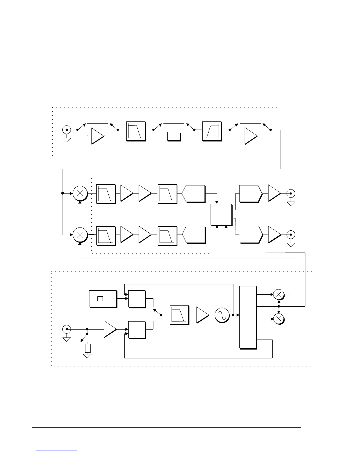
The func tional block diagram of the SR844 RF Lock-In Amplifier is shown below. A
short description of each block follows .
SR844 Block Diagram
RF Signal Path
50 Ω
Signal Input
External
Reference
In
1 MΩ
PreAmp
Mixer 180 kHz
LPF
20 MHz XT AL
Reference
Auto-threshold
Comparator
50 Ω
200 MHz
LPF
I. F . Sec tion
Variable IF
Gain
Anti-alias
Refe r e nc e Cha n ne l
Int Ref
Synthesizer
Ext Ref
Phase
Comparator
20 dB
Attenuator
Filter
Converter
Loop Filter Error
A to D
Amplifier
20 kHz
HPF
X-IF
DSP
Y-IF
200-400 MH z
VCO
20 dB Gain
D to A
Converter
IF Chop
Div id er Chain
CH1
Front Panel
Outputs
CH2
X Ref
IF ChopIF Chop
Y Ref
Ref
SR844 RF Lock-In Amplifier
Page 39

RF Signal Input Path
The path the inpu t s ignal takes from the front panel input to the two mixe rs d epe nds on the
chosen input impedance and wide (RF) reserve. The SR844 accepts input signals in the
range 25 kHz to 200 MHz, with signal le vels up to 1 Vrms (+13 dBm). (T he damage
threshold is 5 V DC+AC.)
Input Impedance
For signal sources with 50 Ω source impedance, the 50 Ω input provide s input matching;
it also provides lower input noise. When using 50
the 50
Ω
input is preferred.
SR844 Basics 2-9
Ω
or other small source impedances,
If the 1 M
preamp with a nominal gain of x2 (+6 dB). The 1 M
source impedance is much greater than 50
Important!
The bandwidth of the 1 MΩ input is limited by its 30 pF input capa citance and the source
impedance. The source impedance (R) and the input capacitance (30 pF) form a s imple
low-pass filter at f
input and not measured accurately by the SR844. Even a 50
106 MHz filter at the 1 M
Ω
|| 30 pF input impedance is selected, the signal is buffered by a FET-input
= 1/2πRC. Signals at frequencies greater than fc are attenuated at the
c
200 M Hz Low Pass F ilt er
This pass ive filter removes signal components above 200 MHz that c ould interfere with
the operation of the SR844.
20 dB Attenuator
This attenuator provides 20 dB (x10) of input signal attenuation. This is useful in cases
whe re the real or interfering s ignals are large. At high sensitivities (near 1 V), the
attenuator is required to s ca le the actua l s ignal to prevent mixer ove rload. A t lower
sensitivities (100 mV and be low), the atte nuator is used to provide wide (RF) dynamic
reserve b y prev enting overloads late r in the signa l pa th. While using the attenuator
deteriorates the noise performance of the instrument, it improves the dynamic reserve.
Ω
input!
Ω
input should only be used if the
Ω
.
Ω
source impedance forms a
20 kHz High Pass Filter
This filter provides a b lock to DC a nd line frequency signals that could interfere with
signal measurement.
20 dB Gain
This gain sta ge can be used to boost low-level signals above the mixer noise floor in
situations where the inte rfering signals a re not too strong. This gain is required for
sensitive measurements (below 100
reserve is needed.
µ
V). It is also used when less wide (RF) dynamic
SR844 RF Lock-In Amplifier
Page 40

2-10 SR844 Basics
Reference Channel
The SR844 accepts sinusoidal and digital signals as external reference inputs, including
low duty-cycle pulse trains. The nominal input levels are 0 dBm sine or 0.7 Vpp pulse.
Larger levels are acceptable. The reference input may be terminated in either 50
10 k
Ω€||€
40 pF.
Auto-Threshold Comparator
The auto-threshold circuit detects the maximum and minimum voltages of the waveform
and sets the thres hold level to the mean of these two voltages. The SR844 uses the
positive tra nsitions through the threshold voltage as its phase reference.
Phase Locked Loop and Divider Chain
The Phase Comparator, Loop Filter, Error A mplifier, VC O a nd Divider Chain form a
classic Phase Locked Loop (PLL). When the output edges of the D ivider Chain coincide
with the output edges of the Auto-T hreshold Compa rator, the loop is phas e -locked.
In the SR844, the VCO always runs be tween 200 and 400 MHz. T he divider chain doe s
succes s ive divide by 2 a ll the way down to 24.4 to 48.8 kHz. In this way, any frequency
within the SR844 operating range ca n be gene rated by s elec ting the appropriate tap from
the chain. In addition, the IF (chopping) frequency is generated synchronously by dividing
the lowes t frequency tap (24–49 kHz) by 3, 4, 12 or 16. The chopping frequency is
between 2–3 kHz for time constants of 1 ms and above, and betwee n 8–12 kHz for 100
and 300
µ
s time constants as well as No Filte r.
Ω
or
20 M Hz Ref erence/ S ynth esizer
In internal reference mode, these components replace the external reference input to the
phase locked loop discuss ed a bove. The synthes izer chip is a phase comparator that can
be programmed to lock when the two inputs (the VCO and the 20 MHz crys tal reference)
are phase-locked at a particular frequency ratio (for example, VCO/194 = 20 MHz/17).
The frequency in inte rnal mode is se t by programming the appropriate ra tio into the
s ynt hesi z er chi p.
Important!
The SR844 provides 3 digits of resolution in setting the internal mode frequency. Because
of the na ture of the fractional arithme tic involved it is not poss ible to generate the exact
frequencies with such a simple configuration. However, the frequency error is less than
0.1 in the 3rd digit. For exa mple, entering an internal frequency of 267 kHz on the front
panel results in a fre quency between 266.9 and 267.1 kHz.
X and Y Reference Generator
The divider chain generates the X and Y squa re wave reference signals , 90° out of phase
at the reference frequency. T hese signals are mixed with the IF chopping signal to produce
the choppe d reference signa ls to the X (in-phase) and Y (quadrature) mixers. T he IF
chopping signa l is pas s e d to the Digital Signal Process or (DSP) to provide the IF
reference.
SR844 RF Lock-In Amplifier
Page 41

IF Section
The mixer outputs contain the in-phase and quadrature components of the input signal,
[shifted to the IF (chopping) frequency (2–12 kHz)] as well as unwanted high-frequency
mixer outp uts a nd contributions from interfering s ignals and input no is e. The IF section
has identical signal paths for the in-phase and quadrature s ignals.
180 kHz Low P ass Fil ter
This pas sive filte r e liminates much of the high-frequency mixer output, principally in
order to ke e p RF out o f the sub s e qu e nt low-frequency a mplifier and filter s ta ges. T his
filter removes the 2f
Gain Stages
A variable IF gain section provides the gain nec e s s a ry to de tec t ve ry weak s ignals. T he
instrument sets the variable gain appropriate to the IF (close) dynamic reserve mode and
overall se nsitivity.
Anti-Aliasing Filter
Digital sampling causes aliasing, where analog signals at high frequencies appear as
digital signa ls a t low frequencies. In ge neral, if the signa l is s ampled at F
signa l at a frequency above F
the anti-aliasing filter is to remove any IF signals above F
mixer output fo r most re fe re nce fre q ue nci e s .
ref
/2 will be aliase d into the interval [0,FS/2]. T he purpose of
S
/2 before digitization.
S
SR844 Basics 2-11
, any input
S
The anti-aliasing filter is a 7th order active C au er filter with a corner at 18 kHz. This filter
is removed when no output filtering is selected .
16-Bit ADC
The analog-to-digital c onverters (AD C s ) digitize the IF outputs for the digital signal
processor (DSP) for further processing. The sampling rate varies be tween 48–96 kHz.
The sampling clock comes from the divider chain in the reference channel and is
synchronous with the reference frequenc y.
SR844 RF Lock-In Amplifier
Page 42
2-12 SR844 Basics
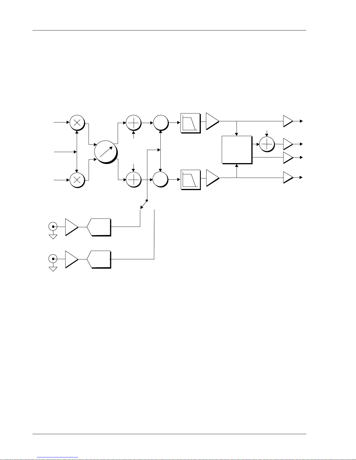
Inside th e DSP
Much of the signal processing in the SR844 occurs ins ide the Digital Signal Processor
(DSP).
I F Demodulator
X-IF
Inside the DSP
÷
X
R offset
IF
Chop
Y-IF
Aux I n 1
Aux I n 2
Inputs
X offset
Ratio
Y offset
Phase
Shift
6, 12, 18, 24
dB/oct Filt er
and G ain
Compute
R an d θ
÷
I F Demodulator
A to D Converter
The DSP receives the digitized X-IF a nd Y-IF signals from the IF s ec tion. In addition
there is an IF chop signal that allows the DSP to demodulate the X-IF and Y-IF signa ls a t
the correct IF frequency.
R
θ
Y
Expands
Demodulators
The two data streams are multiplied by a digital IF chop wa ve form which converts the
X-IF and Y-IF signals back to DC. The advantage of demodulating inside the DSP is to
eliminate the DC output errors of analog mixers.
Phase Adjust
The two demodulated s ignals are subject to a matrix rotation that s e lects the detection
phase (reference phase set by the user) and compensates for phase delays internal to the
ins trument. These phase-rotated signals are hereafter referred to as X and Y.
SR844 RF Lock-In Amplifier
Page 43

Offsets
User entered offsets can be added to X and Y. Thes e offsets are added before taking
ratios, filtering and computing R and
Offsets are useful for making relative measurements or to cancel the contribution from an
unwanted phas e coherent signal. In analog lock-ins, offsets were generally used to remove
DC output errors from the mixer outputs. T he SR844 demodulator is digital and has no
DC output errors, however, it does have coherent pickup a t high frequencies, which can
be canceled using offsets.
Important!
Xoffset and Yoffset are applied to the X and Y before other processing occurs. R and
are computed from the offset values of X and Y. Adding offsets to X or Y changes the
value of R and
In additio n, changing the Reference Pha s e will modify the va lue s of Xoffset and Yoffset.
Think of (Xoffset, Yoffset) as a signal vector relative to the Reference (internal or
external) which cancels an actual signal at the input. This cancellation is preserved even
when the detection phase (Reference Phase) is changed. This is done by circularly rotating
the values of Xoffset and Yoffs et by minus the Reference Phase. This preserves the phase
relationship between (Xoffse t, Yoffset) a nd the signa l input.
SR844 Basics 2-13
θ
.
θ
θ
.
Since the vector (Xoffset, Yoffset) is used to cancel a real signal at the input, Xoffset and
Yoffset are always turned on and off together. T urning either offs e t o n (or off) tu rns o n
(or off) both offs e t s . Au to offset ting either X or Y p e rforms a u to o ffs e t on both quantities.
These s ta tements are true e ven if only one of the q ua ntities X or Y is currently being
displayed.
Ratio
If ratio mode has been selected, the reciprocal of the appropriate input (1.0 V/AUX IN 1
or 1.0 V/AUX IN 2) is computed, and both X and Y are multiplied by this quantity. Since
the value of R is computed after the ratio, R is also scaled by the ratio.
Another application of the Aux Input voltages is to provide a second demodulation,
sometimes known as the Double Lock-In Technique. T his is de s c ribed in the next section.
Time Constant Filters
The signals are filtered by a c hain of simple low-pass filter/amplifiers. Using 1, 2 , 3 or 4
stages provides the selected rolloff of 6, 12, 18 or 24 dB/octave. Dis tributing the gain
among the filte rs a llows near-optimum signal recov ery without causing inte rnal overloads
or losing bits of resolution. The appropriate filte red X and Y are use d for all subse que nt
computations.
The individual filters are the digital equivale nt of an RC low-pass filte r, although be ing
digital they can easily incorporate gain. The numerica l c oe fficients of the filter are chosen
to provide the sele cte d time constant and a gain appropriate to the se nsitivity. Since the
filters are digital, very long time c onstants (up to 30 ks ) are ea s ily a c hievable .
Selecting No Filter removes the filtering operations while leaving jus t gain. This mode is
useful whe n the highest possible analog output bandwidth is required from the X and Y
SR844 RF Lock-In Amplifier
Page 44

2-14 SR844 Basics
outputs. In this c as e , the 18 kHz anti-aliasing filter in front of the IF analog-to-digital
converters is also removed. The output time c onstant is around 20-40
R, θθθθ, dBm Computation
The DSP computes R[Volts] and θ from X and Y, and R[dBm] from R[Volts].
Output Select
Two quantities are s e lec te d for the front panel CH1 and CH2 analog o utputs . These
outputs may be expanded (by 10 or 100) before being s ent to the output digital-to-analog
converters. The outputs are buffered to
The output update rate for X and Y is between 48 and 96 kHz for time constant filter
slopes of 6 and 12 dB/oct as well as No Filter. T he X and Y update rate for 18 and 24
dB/oct filtering is 4 times slower, or 12-24 kHz. The update rate for R and
12-24 kHz.
Two quantities are a ls o s e lec te d for the front panel displa ys . Eac h of these may be
expande d (by 10 or 100) before being se nt to the host proces s or for display and storage.
Th e Host Processor
The host processor provides the interface between the front panel, the instrument
configuration, the DSP and the remote ports (GPIB and RS-232). The host processor
receives the front panel output values from the DSP and displays them and sends the data
to the remote ports. The host also computes X-noise and Y-noise from the X and Y data.
±
10 V.
µ
s in this case.
θ
is als o
SR844 RF Lock-In Amplifier
Page 45

Analog Outputs and Scaling
CH1 and CH2 Ou t put s
The SR844 has two analog outputs, CH1 and CH2, on the front panel. These outputs ca n
be configured to output voltages proportional to the CH1 and CH2 dis plays or X and Y.
X and Y are the traditional outputs of a n analog lock-in. The output vo ltage is
proportional to the X and Y co mponents of the signal with low-pass output filtering,
offset, ratio and expand. In this c as e , a different quantity (R or
shown on the displays.
If the outputs are se t to DISPLAY, the output volta ge is proportional to the quantity
shown on the corresponding display. T he CH1 display can show X, R, R[dBm], Xnoise or
AUX IN 1. The CH2 display can show Y,
ratio and expand may b e a pplie d to many of the s e qua ntities.
Outp ut Scales
The sensitivity of the lock-in is the rms amplitude of an input sine (at the refe rence
frequency) which results in a full scale DC output. Full scale means 10 Vdc at the CH1
or CH2 ana log output. The overall gain (input to output) of the amplifier is then
10 V/sensitivity. T his gain is distributed be tween RF ga in (before the mixer), IF ga in (after
the mixer) and DC gain (in the DSP). Changing the dynamic re s erve a t a given sensitivity
changes the gain distribution while kee ping the ov era ll gain constant.
θ
, Ynoise, Ynoise[dBm] or AUX IN 2. Offset,
SR844 Basics 2-15
θ
for example) may be
The SR844 cons iders 10 Vdc to be full scale for any output proportional to simply X, Y
or R. Values of X, Y and R are always rms values. Noise is also measured in rms Volts
and Xnoise and Ynoise are scaled the same as X and Y.
Phase is a qu antity which ranges from -180
CH2 outputs a voltage proportional to
Outputs proportional to quantities me a s ured in dBm (R[dBm] and Ynoise[ dBm]) have an
output sc ale which is independent of sensitivity. T he output is
20 dBm/V.
Output Offset and Expand
The SR844 ha s the ability to offset the X, Y and R outputs. T his is us e ful when
measuring deviations in the signal around some nominal value. The offset can be set so
that the output is offset to zero. Further changes in the output can then be read directly
from the display or output voltages. The offset is specified as percentage of full scale and
the percentage does not change when the s ensitivity is c hanged. Offsets may be s e t up to
±
110% of full scale. For dBm displays , the offset range is ±110% of 200 dBm or
±
220 dB.
The measured phase may be offset by adjusting the Reference phase.
The X, Y, R and
offset) and multiplies by an expansion factor. T hus, a s ignal which is only 10% of full
scale ca n be expanded to provide 10 V of output rather than only 1 V. The normal use for
θ
outputs may also be expanded. This simply takes the output (minus its
°
to +180° regardless of the sensitivity. When
θ
, the output sc ale is 18°/V or 180° = 10 V.
±
10 V = ±200 dBm or
SR844 RF Lock-In Amplifier
Page 46

2-16 SR844 Basics
expand is to expand the meas urement resolution around some value which is not zero. For
example, suppos e a s ignal has nominal value of 0. 9 mV and we want to measure small
deviations, say 10
to accommodate the nominal signal. If the offset is set to -90% of full scale, the nominal
0.9 mV signal will result in a zero output. T he 10
100 mV of output. If the output is e xpanded by 10, these s mall deviations are ma gnified
by 10 and provide 1 V of output.
The SR844 can e xpand the output by 10 or 100 provided the expanded output does not
exceed full s cale. In the above example, the 10
times before they exceed full scale (1 mV sensitivity).
Outputs proportional to quantities measured in dBm (R[dBm] and Ynoise[ dBm]) may
also be expanded. The expande d output sca les are 2 dB/V and 0.2 dB/V for x10 and x100
expands.
µ
V or so, in the signal. The se nsitivity of the lock-in needs to be 1 mV
µ
V deviations in the signal only provide
µ
V deviations ca n be expanded by 100
The phase output ma y als o be e xpanded on C H2. The expanded output scales are 1.8
and 0.18
°
/V for x10 and x100 expa nds. T he phase output can not be offset. Instead us e
the Reference phase to adjust the detection phase to yield a measured phas e of zero.
Disp lay Scales
Offsets are reflected in the dis played values. For example, if CH1 is displaying X, the X
offset is a pplie d to the dis pla yed va lue . When X is offse t to zero, the displaye d va lue will
drop to zero also. Any displa y which is showing a quantity which is affec te d by XY
offsets will displa y a highlighted XYOffs indicator below the value. If the quantity is
affected by an R offset, the ROffs indicator will be on. Note that both indicators may be
on at the same time.
Output expands do not increase the displayed values. Expand increases the resolution of
the displayed value (not the size of the displa yed s ignal). When X is expanded, the
display is shown with more digits but has the s a me non-expanded value. Any display
whic h is expanded will display a highlighted Expand indicator below the value .
°
/V
SR844 RF Lock-In Amplifier
Page 47

What is Dyn a mic Reserve ?
Dynamic reserve is an important concept for lock-in amplifiers. It is a measure of how
much noise, or interfering s ignals at frequencies other than the re ference, the instrument
can withs ta nd while s till accurately measuring the desired signal at the reference
frequency. More dynamic reserve is b ette r. T he traditional definition of dyna mic rese rve
is the ratio of the largest tolerable noise s ignal (at the input) to the full sc ale s ignal,
expressed in dB. For example, if full scale is 1
means noise as large as 1 mV (1000 time s greater than 1
without overload.
Unfortunately, the word ‘tolerable’ allows some latitude in usage. Even without causing
overloads, large interfering signals can cause distortion and DC output errors in analog
components that can affect the measurement. For this discussion, dynamic reserve is
defined as follows :
The dynamic reserve of a lock-in amplifier at a given full-scale input voltage is the ratio
(in dB) of the Large s t Interfering Signa l to the full-sca le input voltage. The Largest
Interfering Signal is defined as the amplitude of the largest interfering signal (not a t the
reference frequency) that can be applied to the input before the lock-in cannot measure a
signal with its specified accuracy.
µ
SR844 Basics 2-17
V, then a dynamic reserve of 60 dB
µ
V) can be tolerated at the input
While dynamic reserve is quoted as a s ingle number, the a ctual res erve de pends upon the
frequency of the interfering s ignal. The reas on for this has to do with the fact that a lockin amp lifier app lies (1) gain and (2) band width-na rrowing to the input signal, and it does
so in s e veral sta ges . De pending on their frequ e ncy, d iffe re nt interfe ri ng signals are
reje c te d a t d ifferent poi nts. An interferi ng signal se ve ral MHz from the refe re nce p rod u c e s
a mixe r outpu t at s e ve ral MHz; this s ignal is rejected b y the IF low-pa s s filter
immedia t e ly fol lo wing the mixer. A n interfering signal 50 kHz from the refere nce is
rejected b y the anti-aliasing filter before the A-D converter (see the following sectio n for
a detaile d functional desc ription). A clos e -by interfering s ignal is rejecte d by the timeconstant filters in the DSP. Note: What about an interfe ring signal a t 6 Hz offset, when the
time-constant is only 3 ms ? 3 ms corresponds to a bandwidth of a bout 330 s
this signa l is within the instrument bandwidth and by definition is not an i nterf er ing si gnal.
Wi de and Clo se Reserves
The fact that gain and bandwidth-narrowing occur in s everal stages leads to the question
of how best to allocate the gain between the different stages. At one extreme, one could
imagine all the gain to be in the D SP (digital signal processor), which wins with regard to
dynamic reserve since interfering s ignals suffer no amplification and a re le a s t like ly to
caus e ov erloa ds or dis to rtion. The drawback to this is that the signal could get lost in the
noise at the A-to-D converter or mixer. (In analog lock-ins, the DSP gain was replaced by
output DC gain, which caus e d s ubsta ntial problems with DC offset and drift). T he other
extreme is to put the maximum gain as close to the signal input as possible; this approach
wins on noise performance, but has poor dyna mic reserve. Since the interfering s ignals see
lots of gain, a relatively small interfering signal could caus e a n overload.
-1
≅ 50 Hz,
SR844 RF Lock-In Amplifier
Page 48

2-18 SR844 Basics
Recognizing that differe nt experimental situations call for different gain-allocation
strategies, the SR844 provides multiple dynamic res e rve modes se parate ly for both the
RF signal gain (before the mixer) and the IF gain (after the mixer).
Wide Reserve or RF reserve, allocates the RF signal gain before the mixer. See Chapter 3,
Signal Input, for a table of RF gain vs Wide Reserve. The Wide Reserve should be set to
accommodate all interfering s ignals within the 20 kHz - 200 MHz bandwidth of the RF
input. High reserve a pplie s minimum RF ga in preventing la rge interfering signals from
causing amplifier overloads. Low Noise provides maximum RF gain and the best output
signal-to-nois e a nd is les s sus c e ptible to c oherent pick-up. Normal is in between.
Close Reserve or IF reserve, allocates the IF gain after the mixer and before the DSP. The
Close Reserve should be set to accommodate interfering signals closer to the reference
frequency than the IF bandwidth (180 kHz). High res erve a pplies the minimum IF gain
preventing overloads before the DSP. Low Noise provides the maximum IF gain and the
best output signal to noise. Normal is once again somewhere in between. T he maximum
allowable IF gain is proportional to (sensitivity x RF gain)
Choosing the Wide Reserve sets the RF gain (see Chapter 3, Signal Input) and thus
determines the maximum a llowable IF gain. The minimum IF gain is 1.
-1
- up to a maximum of 50 dB.
After sele cting the Wide (RF) and Clo s e (IF) reserve modes, the DSP supplies the
remainder of the ga in required for the correct output sc aling.
Important!
As a general rule, try to use Low Noise reserve modes if pos s ib le. Only increase the
reserve if ove rloa ds oc c ur. T his will provide the best outpu t s ignal-to-noise and have the
least coherent pickup (see below).
Some sensitivity settings do not ha ve three different gain a lloc a tions ava ila ble. For
example, the 1 V se nsitivity ca n only be achieved by a s ingle gain a lloc a tion. Sensitivity
µ
settings below 10
V require all of the available gain. In these cas es two, and sometimes
all three, of the reserve modes actually use the same gain allocation. T he dynamic reserve
of these identical gain allocations is, of course , the same.
Note that the 1 Vrms input specification should never be exceeded in a measurement
situation. T his means that when the sensitivity is 1 Vrms, the re is no room left for
interfering signals, and the dynamic reserve is zero!
SR844 RF Lock-In Amplifier
Page 49

Sources of Error
Spurious Respon ses
It is useful to consider the signal in the frequency domain. Fourier’s theorem states that
any signal can be represented as an infinite sum of sine waves, each with different
frequency, amplitude and phase. In the fre quency domain, a s ignal is described in terms of
its individual frequency components. This is in contrast to the time doma in desc ription,
where the s ignal is described by its value at each point in time, just like one would see on
an oscilloscope. The SR844 circuitry is linear, whic h means that the signal at any point is
the s um of the s ignals due to each frequency component. For the purpose of analysis the
individual frequency components may be treated independently.
The SR844 multiplies the signal by a (choppe d) squa re wave at the reference frequency.
All components of the input signal a re multiplied by the reference frequency
simultaneous ly. Signal and noise at the reference frequency give rise to (chopped) DC. In
general other frequency components give rise to mixer outputs at other frequencies, and
are not detected. There are a few exceptions, whic h constitute the spurious response of
the instrument. It is good for a user to be aware of and understand these limitations .
SR844 Basics 2-19
Spurious responses are outputs due to signals at frequencies other t han the refe re nce
frequency. These outputs are indistinguishable from the output due to a signal at the
refere nce fre q u e ncy.
Square Wave Response
The first class of spurious responses a re harmonics of the reference frequency. Recall that
the mixer multiplies the input signa l by the lock-in reference, whic h is really a s qua re
wave. A s qua re wave a t the reference frequency may be written as
sin(ω
t) + (1/3) sin (3ωRt) + (1/5) sin (5ωRt) + …
R
The lock-in is de tecting signals at all odd harmonics of the reference simultaneously. An
input signal a t 3
at the third harmonic is a fundamental limitation of the tec hnique employed in the SR844.
When the input s ignal is also a square wave (at the reference frequency), all of the odd
harmonics of the signal coincide with the harmonics of the reference and are detected. In
the frequency domain, this is s imply multiplying eqn. 2-18 by its elf a nd keeping tho s e
resultant terms which a re at DC . T hus, the contribution from all odd harmonics is
1 + (1/3)
2
The amplitude of the fundamental sine component of a square wave is 4/
amplitude of the square wave. The detected amplitude is 4/
The SR844 reads the signa l in units of Vrms (0.707 x 1. 53 x peak) or 1.08 x peak (Vrms).
ω
yields an output 1/3 as large as a signa l at
R
+ (1/5)2 + (1/7)2 + ... ≈ 1.2
(2-18)
ω
. This –10 dB response
R
π
x the peak
π
x peak x 1. 2 or 1.53 x peak.
IF Sidebands
The second class of spurious res ponses are c hopping sideba nds at
the chopping fre quency (IF) and N is an integer. To understand these spurious responses,
we need to understand a little more about how chopping works . T he chopping operation
ω
±2N
R
ω
, where
C
ω
is
C
SR844 RF Lock-In Amplifier
Page 50
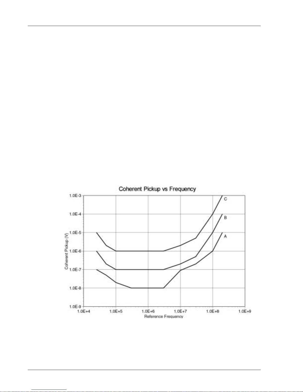
2-20 SR844 Basics
consists of multiplying a signal by a s qu are wave of amplitude 1 and frequency ωC. Half
of the time the output eq ua ls the input. The other half of the time the output is the
negative of the input. Assuming that all chopping operations a re properly synchronized,
we can take a signal, chop it, and chop it again and recover the original signal.
Now let’s take a reference s ignal at
reference input, where it gets multiplied by the signal input. Without c hopping, the mixer
output would have a D C output proportional to the s ignal input. With chopping, the DC
output is multiplied by ±1 at the chopping frequency. If we now chop this output we ca n
recover the DC output. Howeve r, the chopping operations are not ideal and signals a t
frequencies other than the reference can cause DC outputs from the final chopping
operation. The spurious responses are typically –10 dB at a frequency offs e t of
dropping to -30 dB at ±6f
Coherent Pickup
At the high reference frequencie s use d by the SR844, a sma ll amount of referenc e s ignal
pickup occurs in the RF signa l path. This is called c oherent pickup. Sinc e the pickup is
phase coherent with the reference frequency it is detected by the SR844 as if it was a real
s i gnal i npu t. Measuring si gnals whi ch ar e smal l er t han t he i nstrument ’ s own co her ent
pickup requires care and the use of offsets.
The typical amount of coherent pickup in the SR844 is shown below.
ω
ω
≈ ω
(
1
and -42 dB at ±12fC where fC is in the range of 2-12 kHz.
C
), chop it and put it into the mixe r
1
C
±
2fC,
The level of coherent pickup (three curves above) is dependent on the RF input gain. The
choice of Wide (RF) reserve a nd Sensitivity determines the RF gain a nd thus, the level of
coherent pickup. T he following table shows which curve to use.
SR844 RF Lock-In Amplifier
Page 51
SR844 Basics 2-21
50 ΩΩΩΩ Si g Z-In 1 MΩΩΩΩ Si g Z-In
Wide
Reserve
Sensitivity
1 V C C C C C C
300 mV C C C C C C
100 mV C B B C C B
30 mV C B B C B B
10 mV C B A B B A
3 mV C B A B B A
1 mV C B A B A A
300 µV
100 µV
30 µV
10 µV
3 µV
1 µV
300 nV A A A A A A
100 nV A A A A A A
HIGH NORMAL LOW
HIGH NORMAL LOW
NOISE
BA A BA A
BA A BA A
BA A AA A
AA A AA A
AA A AA A
AA A AA A
NOISE
Clearly the Low Noise res e rve s etting should be used whenever possible. For sensitive
measurements, the Low Noise reserve c an provide 60 dB or more of dynamic res e rve
while minimizing the cohe rent pickup.
Another source of coherent pickup is in the expe rimental setup itself. T he signal and
reference cables and grounds are very important, especially at higher reference
frequencies.
The X and Y offsets ca n be used to cancel the coherent pickup as long as the pickup
remains sta ble during the experiment.
SR844 RF Lock-In Amplifier
Page 52

2-22 SR844 Basics
Using th e SR844 as a Dou ble Lock-In
The ratio feature of the SR844 can be used to provide a sec ond stage of demodula tion.
Consider the following application: you ha ve a n experiment providing a signal at
100 MHz. Because the environment is nois y and RF interference is everywhere, you
arrange the experiment so that the s ignal of interest is modulated at a low frequency, sa y
on/off at 100 Hz. T his could be a las er beam with a 100 MHz pulse rate going through a
light chopper spinning at 100 Hz. The problem is to mea s ure the modulated compone nt of
the 100 MHz s ignal.
One solution is to us e a 100 MHz power meter to me as ure the signa l, and put its 100 Hz
output into a traditio nal low-frequency loc k-in suc h as a n SR830 and meas ure the 100 Hz
component. Or you could put the signal into an SR844 and make a narrowband
measurement at 100 MHz, using a 1 ms time constant, and take the 100 Hz analog output
and look at it with either an oscilloscope or a low-frequ e ncy l ock-in. O r you could have
the SR844 dete ct both the 100 MHz and 100 Hz signals a s follows: put the 100 Hz
reference signal into the SR844’s AUX IN 1 input, turn on ra tio mode, and have the
SR844 make the measurement for you directly, say with a 1 s time constant.
The key to this technique, sometime s referred to as a double loc k-in, is putting in a
bipolar square wave into AUX IN 1. Remember that the DSP is dividing the incoming
data by AUX IN 1, and the n low-pass filtering the res ult. If AUX IN 1 is
effectively demodulating the 100 Hz output and averaging it.
±
1 V, the D SP is
In order to get accurate measurements of the 100 Hz modulated component of the
100 MHz signal, it is importa nt that any unmodulated 100 MHz signal be rejec ted. You
can do this by turning off the 100 MHz modulation and adjusting the DC offset of the
AUX IN 1 square wave until the SR844 rea ding is nulled. In the above example , simply
turn off the light chopper and pass the beam 100% of the time. If the AUX IN 1 signal
comes from a s ource that allows independent phase adjustment without disturbing the
experiment, you can also perform the following test: cha nge the phase of the AUX IN 1
source by 180
but stay at the same value.
While the use of AUX IN 1 for demodulation can be a handy technique, it does suffer
from two limitations. First, the AUX IN 1 input is bandwidth limited to about 3 kHz
(minimum sampling rate is 12 kHz), so the modulation signal into AUX IN 1 should be
considerably slower than this, say up to a few hundred Hz. Second, there is no phase
adjustment on the ratio input. Remember, the X and Y outputs are both modulated at the
same phas e of the 100 Hz modulation. In the above example, they both turn on and off
together with the light chopper. If the ratio input is 90° out of phase with the this
modulation, the result is zero on both X a nd Y .
In genera l, u s i ng a low-freque ncy lo c k -in amplifie r i s p re fe rre d . However, in many
instanc es , the SR844 provides a convenient s olution for both modulation frequencies.
°
— if the signal is properly nulled, the instrume nt reading will change sign
SR844 RF Lock-In Amplifier
Page 53
Noise Measurements
Lock-in amplifiers can be used to measure noise. Noise measurements are usually used to
characterize components and detectors.
The SR844 meas ures input signal noise at the reference frequency. Many noise sources have
a frequency dependence which the lock-in can measure.
How Does a Lock-in Measure Noise ?
Remember that the lock-in detects signals close to the reference frequency. How close? Input
signals within the detection bandwidth se t by the time constant and filter rolloff appear at the
output at a frequency f=f
the output with a bandwidth of DC to the detection ba ndwidth.
For Gauss ia n noise, the equivalent noise bandwidth (ENBW) of a low-pass filte r is the
bandwidth of a pe rfec t rec tangular filter which passes the same amount of nois e a s the real
filter. The ENBW is determined by the time constant and s lope a s s hown below.
Slope [dB/octave] ENBW for Time Constant T
SIG–fREF
. Input noise near the reference frequency appears as noise at
6 1/(4T)
12 1/(8T)
18 3/(32T)
24 5/(64T)
SR844 Basics 2-23
Noise Estimation
The noise is simply the standard deviation (root of the mean of the squared deviations) of the
measured X or Y. This formula, while mathematically exact, is not suited to providing a realtime output proportional to the measured noise. Therefore the SR844 uses a s implified
algorithm to estimate the X or Y noise.
The moving average of X is computed over some past history, and subtracted from the
present value X to get the deviation. The Mean Average Deviation (MAD) is computed as a
moving average of the absolute value of the deviations. For Gaussian noise, the MAD is
related to the RMS deviation by a constant factor. The MAD is scaled by this factor and by
the ENBW to obta in noise in units of Vo lts /
Volts/
√
Hz. The average reading is independent of the time constant and slope but the
variations or noisiness in the reading is not. For more stable rea dings, use longer time
constants.
In the SR844 the X a nd Y noise are computed in the host processor; the MAD algorithm is
used because it requires less computation and is a moving average. T he X and Y data values
are s a mple d (fro m the DSP) at a 512 Hz rate; the moving average and MAD a re then
updated. T he moving averages have an exponential time cons tant that varies between 10 to
80 times the filter time constant. Shorter averaging times s e ttle quic kly b ut fluctu ate a lot a nd
yield a poor estimate of the noise, while longer averaging times yield better noise estimates
but take a long time to s e ttle to a s te a dy a nswer.
The SR844 performs the nois e calc ulations all the time, whether or not X or Y noise is being
displayed. T hus, as soon as X noise is displayed, the value shown is up to date and no extra
√
Hz. X and Y noise are displaye d in units of
SR844 RF Lock-In Amplifier
Page 54

2-24 SR844 Basics
settling time is required. If the sensitivity (or other mea s ure ment parameter) is changed, the n
the noise es timate will need to settle to the correct v alu e.
SR844 RF Lock-In Amplifier
Page 55

Intrinsic (Ran dom) Noise Sources
Random noise finds its way into experiments in a variety of ways . Good e xperimental design
can reduce these noise s ource s a nd improve the me as u rement stability and accuracy.
There are a variety of intrinsic noise sources which are present in all electronic signals.
These sources are physical in origin.
Johnson Noise
Every resisto r generates a noise volta ge acros s its terminals due to thermal fluctuations in the
electron density within the res is tor its e lf. These fluctua tions give rise to a n open-circuit noise
voltage
SR844 Basics 2-25
V
(rms) =
NOISE
whe r e k i s Bol tzmann’ s co nstant ( 1.38 x10
√ (4kTR∆f)
–23
JK–1), T is the absolute te mperature (typica lly
300 K), R is the resistance in ohms and ∆f is the measurement bandwidth in Hz.
The amount of noise measured by the lock-in is determined by the measurement bandwidth.
In a loc k-in the equivalent noise bandwidth (ENBW) of the time constant filters se ts the
measurement bandwidth. The ENBW is determined by the time constant and slope as shown
previously.
The Johns on noise of a 50
(rms ) = 0.91 nV × √ (ENBW)
V
NOISE
Ω
input on the SR844 is simply
Shot Noise
Electric current has noise due to the finite nature of the charge carriers. There is always some
non-uniformity in the elec tron flow which gene rate s noise in the current. This noise is ca lle d
shot noise. This can appear as voltage noise when current is passed through a resistor. The
s hot noi se o r cu r r ent no ise i s giv en b y
I
(rms) =
NOISE
where q is the electron charge (1.6×10
measurement bandwidth.
√(2qI
RMS
∆f)
–19
C), I
is the rms current and ∆f is the
RMS
(2-20)
(2-21)
1/f Noise
Every 68 Ω resisto r, no ma tte r what it is made of, ha s the sa me Johnson nois e . However there
is additional noise, asid e from the Johns on noise, which arises from resistance fluctua tions
due to the current flowing through the resistor. This noise has spec tral p ower density
inversely proportional to the frequency, he nce the name. The amount of 1/f nois e is
dependent on the res istor material and even manufac turing details. For ca rbon composition
resisto rs this noise is typic a lly 0. 3
resistors 0.01
Ω
, the µV/V numbers are worse for large resistances.
To t al Noise
All of these noise sou rce s are incoherent. The total random nois e is the square root of the
sum of the squares of all the incoherent noise sources.
µ
V/V per decade of frequency, while for leaded metal film
µ
V/V is more typical. These numbers are for low resis tance values 10–1000
SR844 RF Lock-In Amplifier
Page 56

2-26 SR844 Basics
External Noise Sou rces
In additio n to the intrinsic noise sources d is cu s s e d in the previous se c tion, there are a
variety of external noise s ources within the laboratory.
Many noise sources are asynchronous , i.e. they are not related to the reference and do not
occur at the reference frequency or its harmonics. Examples include lighting fixtures,
motors, cooling units, radios and computer screens . T hese noise sources affect the
measurement by increasing the required dynamic reserve or time cons tant.
Some noise sources , however, are related to the reference and, if picked up in the signal
path, will a dd o r su btrac t from the actual signal and cause errors in the measure ment.
Typical source s of s ynchronous noise are ground loops between the experiment, detector
and lock-in, and electronic pick-up from the refere nce os cilla tor or experimental apparatus
and cables.
Many of these noise sources ca n be reduced with good laboratory prac tice a nd experiment
design. There are several ways in which noise sources a re coupled into the signal path.
Capaci t ive couplin g
An RF or AC voltage from a nearby piece of apparatus can couple to a detector via a
stray capacitance. Although C
a weak experimental signal. T his is es pec ially damaging if the couple d noise is
synchronous (i.e. at t he re fe re nce fre q ue ncy ).
may be very small, the c oupled noise may still exceed
STRAY
Cstray
Detector
Signal
Source
Noise
Source
We can estimate the noise current caused by a stray capacitance by
I=
where
× (dV/dt) = ω⋅ C
C
STRAY
ω/2π
is the noise frequency, V
STRAY
NOISE
⋅V
NOISE
is the noise amplitude, and C
STRAY
(2-22)
is the stray
capacitance. T his type of coupling is e s pec ially damaging since it is proportional to
frequency and the SR844 operates at very high frequencies.
For example, if the noise source is a computer clock line,
V
might be 5 V/2. C
NOISE
capacitor, perhaps 0.1 cm
resu lt ing no ise cur r ent is 0 .5
can be crudely estimated using a parallel plate equivalent
STRAY
2
at a distance of 10 cm, which yields C
µ
A, or 25 µV across 50 Ω.
ω
/2π might be 33 MHz and
–15
STRAY
≅ 10
F. T he
If the noise source is at the reference frequency, then the problem is much worse. The
lock-in rejects nois e at other frequencies, but pick-up at the reference signal appears as
s i gnal !
SR844 RF Lock-In Amplifier
Page 57

Cures for capa citive coupling inc lude :
• Removing or turning off the nois e s ource.
SR844 Basics 2-27
• Keep the noise source far from the experiment (reducing C
cables close to the noise source or reference cables.
• Desi gning t he expe ri ment wit h lo w- imp edanc e det ect ors (so that noi se cu r re nt generate s
small voltages).
• Installing c ap ac itive s hielding by placing both the experime nt and detector in a metal
box.
Inductive coupling
An AC current in a nearby piece of apparatus can couple to the experiment via a magnetic
field. A changing current in a nearby circuit gives rise to a changing magnetic field, which
induces an EMF (d
like a transformer with the experiment–detector loop as the secondary winding.
). Do not bring si gnal
STRAY
Φ
/dt) in the loop conne cting the detec tor to the experiment. This is
B
B(t)
Detector
Signal
Source
Noise
Source
Cures for inductively coupled nois e include:
• Re mo vi ng or tu r ning o ff the i nte rfer ing no ise so ur ce.
• Reducing the area of the pick-up loop by using twisted pairs or coaxial cables.
• Using magne tic shielding to p reve nt the magne tic field from crossing the area of the
experiment.
Resistive coupling or Ground Loops
Cur r ents f l owing t hr ou gh gr ound conne cti ons ca n giv e r ise t o no ise v ol ta ges. This i s
especially a problem with reference frequency ground currents .
Detector
Noise
Source
Signal
Source
SR844 RF Lock-In Amplifier
Page 58

2-28 SR844 Basics
In this illustration, the detector is meas uring the s ignal relative to a ground far from the
rest of the experiment. T he dete c tor s enses the signal plus the voltage due to the noise
source’s ground return passing through the finite res is tance of the ground between the
experiment and the detector. The detector and the experiment are grounded at different
places which, in this case, are at different potentials.
Cures for ground loop problems inc lude:
• Grounding everything to the sa me physical point.
• Using a heavy ground bus to reduce the res ista nce of ground connections.
• Removing sources of large ground currents from the ground bus used for small signals.
Microphonics
Not all sources of noise are electrical in origin. Mechanical noise can be translated into
electrical noise by microphonic effects. Physical changes in the experiment or cables (due
to vibrations , for example ) can result in electrical nois e at the lower end of the SR844’s
operating frequency range.
For example, consider a coaxial cable connecting a detector to the lock-in. T he
capacitance of the cable is a function of its geometry. Mechanical vibrations in the cable
translate into a capacitance that varies in time at the vibration frequency. Since the cable
is governed by Q = C⋅V. Taking the components of this equation at the vibration
frequency , we have Q
the load resistance on the cable, and solve for V
=
V
ν
– C
⋅V
/[C0+j/(ωR)]
ν
0
This assumes a DC voltage (V
= C
ν
⋅V
ν
⋅V
+ C
0
) present on the cable. In general a cable s ubject to
0
. We can also use Vν = R⋅Iν = jωQν, where R is
ν
0
ν
(2-23)
vibration acts as a mixer, generating signal components at the sum and difference of the
vibration frequency and any electrical signal fre quency.
Some ways t o mini mize microphoni c signal s are :
• Eliminate mechanical vibrations near the experiment.
• Tie down cables c a rrying sensitive signals s o they do not move.
• Use a low noise cable that is designed to reduce microphonic effects.
SR844 RF Lock-In Amplifier
Page 59

Chapter 3
Operatio n
In This Chapter
3-1
Overview 3- 3
Power 3-3
Reset 3-3
Keys 3-4
Key-Click On/Off 3-4
Keypad Test 3-4
Knob 3-4
Local Lockout 3-5
Front Panel Display Test 3-5
Display Off Operation 3-5
Front Panel Connectors 3-5
Rear Panel Connectors 3-6
Factory Preset Values 3-7
Signal Input 3-8
Time Constants 3- 11
Sens itivity 3-1 3
CH1 Display and Output 3-15
CH2 Display and Output 3-21
Reference Section 3-27
Save and Recall 3-31
Interface 3-32
Scan and Rel 3-34
Overview 3-34
Using Frequency Scans 3-35
Storing and Using Rel Values 3-36
Scan and Rel Example 3-39
Rels without Scan 3-40
Auto Functions 3-41
Shift Functions 3-42
SR844 RF Lock-In Amplifier
Page 60

3-2 Operation
SR844 RF Lock-In Amplifier
Page 61
Overview
Overview 3-3
CH1 Display CH2 Display Reference Displa y
TIME CONSTANT
TIME CONSTANT
TIME CONSTANT
TIME CONSTANT
TIME CONSTANT
TIME CONSTANT
FILTER OVLD
FILTER OVLD
FILTER OVLD
FILTER OVLD
FILTER OVLD
FILTER OVLD
3x1x10
3x1x10
3x1x10
3x1x10
3x1x10
3x1x10
1
1
1
1
1
1
SETTLE...
SETTLE...
SETTLE...
SETTLE...
SETTLE...
SETTLE...
SIGNAL INPUT
SIGNAL INPUT
SIGNAL INPUT
SIGNAL INPUT
SIGNAL INPUT
SIGNAL INPUT
RF OVLD
RF OVLD
RF OVLD
RF OVLD
RF OVLD
RF OVLD
50 Ω
50 Ω
50 Ω
50 Ω
50 Ω
50 Ω
1 MΩ
1 MΩ
1 MΩ
1 MΩ
1 MΩ
1 MΩ
15 pF
30 pF
30 pF
30 pF
15 pF
30 pF
Sig
Sig
Sig
Sig
Sig
Sig
Z – In
Z – In
Z – In
Z – In
Z – In
Z – In
SIGNAL
SIGNAL
SIGNAL
SIGNAL
SIGNAL
SIGNAL
IN
IN
IN
IN
IN
IN
25 kHz –
25 kHz –
25 kHz –
25 kHz –
25 kHz –
25 kHz –
200 MHz
200 MHz
200 MHz
200 MHz
200 MHz
200 MHz
ks
ks
ks
ks
ks
ks
x100
x100
x100
x100
x100
x100
s
s
s
s
s
s
ms
ms
ms
ms
ms
ms
µs
µs
µs
µs
µs
µs
WIDE RESERVE
WIDE RESERVE
WIDE RESERVE
WIDE RESERVE
WIDE RESERVE
WIDE RESERVE
HIGH
HIGH
HIGH
HIGH
HIGH
HIGH
NORMAL AUTO
NORMAL AUTO
NORMAL AUTO
NORMAL AUTO
NORMAL AUTO
NORMAL AUTO
LOW NOISE
LOW NOISE
LOW NOISE
LOW NOISE
LOW NOISE
LOW NOISE
NO FILTER
NO FILTER
< 1 V rms
< 1 V rms
< 1 V rms
< 1 V rms
< 1 V rms
< 1 V rms
5 V DC+AC
5 V DC+AC
5 V DC+AC
5 V DC+AC
5 V DC+AC
5 V DC+AC
MAX
MAX
MAX
MAX
MAX
MAX
NO FILTER
NO FILTER
NO FILTER
NO FILTER
NO FILTER
NO FILTER
6 dB/Octave
6 dB/Octave
6 dB/Octave
6 dB/Octave
6 dB/Octave
6 dB/Octave
12
12
12
12
12
12
18
18
18
18
18
18
24
24
24
24
24
24
AUTO
AUTO
AUTO
AUTO
AUTO
AUTO
+13dBm
+13dBm
+13dBm
+13dBm
dBm
dBm
dBm
dBm
dBm
dBm
-67
-67
-67
-67
-67
-67
-87
-87
-87
-87
-87
-87
-107
-107
-107
-107
-107
-107
-127
-127
-127
-127
-127
-127
STANFORD RESEARCH SYSTEMS
STANFORD RESEARCH SYSTEMS
STANFORD RESEARCH SYSTEMS
STANFORD RESEARCH SYSTEMS
STANFORD RESEARCH SYSTEMS
STANFORD RESEARCH SYSTEMS
SENSITIVITY
SENSITIVITY
SENSITIVITY
SENSITIVITY
SENSITIVITY
SENSITIVITY
IF OVLD
IF OVLD
IF OVLD
IF OVLD
IF OVLD
IF OVLD
AUTO
AUTO
AUTO
AUTO
AUTO
AUTO
AUTO
AUTO
AUTO
AUTO
AUTO
AUTO
FULL SCALE
FULL SCALE
FULL SCALE
FULL SCALE
FULL SCALE
FULL SCALE
100µ
100µ
100µ
100µ
100µ
100µ
30µ
30µ
30µ
30µ
30µ
30µ
10µ
10µ
10µ
10µ
10µ
10µ
3µ
3µ
3µ
3µ
3µ
3µ
1µ
1µ
1µ
1µ
1µ
1µ
300n
300n
300n
300n
300n
300n
100n
100n
100n
100n
100n
100n
HIGH
HIGH
HIGH
HIGH
HIGH
HIGH
NORMAL
NORMAL
NORMAL
NORMAL
NORMAL
NORMAL
LOW NOISE
LOW NOISE
LOW NOISE
LOW NOISE
LOW NOISE
LOW NOISE
Close
Close
Close
Close
Close
Close
Resrv
Resrv
Resrv
Resrv
Resrv
Resrv
AUTO
AUTO
AUTO
AUTO
AUTO
AUTO
OVLD
OVLD
OVLD
OVLD
OVLD
OVLD
ERROR
ERROR
DIAG
DIAG
V [rms]
V [rms]
V [rms]
V [rms]
V [rms]
V [rms]
1
+13
1
+13
1
+13
1
+13
1
+13
1
+13
300m
300m
300m
300m
300m
300m
100m
-7
100m
-7
100m
-7
100m
-7
100m
-7
100m
-7
30m
30m
30m
30m
30m
30m
10m
-27
10m
-27
10m
-27
10m
-27
10m
-27
10m
-27
3m
3m
3m
3m
3m
3m
1m
-47
1m
-47
1m
-47
1m
-47
1m
-47
1m
-47
300µ
300µ
300µ
300µ
300µ
300µ
Expand
Expand
Expand
Expand
Expand
Expand
CAL
Rel
REL
REL
CAL
Offset
XY Offs R Offs
XY Offs R Offs
XY Offs R Offs
Offset
XY Offs R Offs
X
OVERFLOW
X
OVERFLOW
X
OVERFLOW
X
OVERFLOW
X
OVERFLOW
X
OVERFLOW
UNDERFLOW
UNDERFLOW
UNDERFLOW
UNDERFLOW
UNDERFLOW
UNDERFLOW
R [V]
R [V]
R [V]
R [V]
R [V]
R [V]
R [dBm]
R [dBm]
R [dBm]
R [dBm]
R [dBm]
R [dBm]
X noise
AUX IN 1
X noise
AUX IN 1
X noise
AUX IN 1
X noise
AUX IN 1
X noise
AUX IN 1
X noise
AUX IN 1
AUX IN 1
AUX IN 2
AUX IN 1
AUX IN 2
AUX IN 1
AUX IN 2
AUX IN 1
AUX IN 2
AUX IN 1
AUX IN 2
AUX IN 1
AUX IN 2
Display Ratio Expand Output
Display Ratio Expand Output
Display Ratio Expand Output
Display Ratio Expand Output
Display Ratio Expand Output
Display Ratio Expand Output
OFFSET
OFFSET
OFFSET
OFFSET
OFFSET
OFFSET
On/Off Auto Modify
On/Off Auto Modify
On/Off Auto Modify
On/Off Auto Modify
On/Off Auto Modify
On/Off Auto Modify
REL
x10
x10
x10
x10
x10
x10
x100
x100
x100
x100
x100
x100
CH1 OUTPUT
CH1 OUTPUT
CH1 OUTPUT
CH1 OUTPUT
CH1 OUTPUT
CH1 OUTPUT
CHANNEL ONE
CHANNEL ONE
CHANNEL ONE
CHANNEL ONE
CHANNEL ONE
CHANNEL ONE
OVLDCAL
OVLD
OVLD
OVLD
OVLDCAL
OVLD
DISPLAY
DISPLAY
DISPLAY
DISPLAY
DISPLAY
DISPLAY
X
X
X
X
X
X
<20mA <20mA
<20mA <20mA
<20mA <20mA
<20mA <20mA
<20mA <20mA
<20mA <20mA
Model SR844 RF Lock-In Amplifier
Model SR844 RF Lock-In Amplifier
Model SR844 RF Lock-In Amplifier
Model SR844 RF Lock-In Amplifier
Model SR844 RF Lock-In Amplifier
Model SR844 RF Lock-In Amplifier
OVLD
OVLD
OVLD
OVLD
OVLD
OVLD
Ratio
Ratio
Ratio
Ratio
Ratio
Ratio
V
V
V
V
V
V
mV
mV
mV
mV
mV
mV
TRIG
TRIG
TRIG
TRIG
TRIG
TRIG
µVdBm
µVdBm
µVdBm
µVdBm
µVdBm
µVdBm
FREQ
FREQ
FREQ
FREQ
FREQ
FREQ
nV
nV
nV
nV
nV
nV
pV
pV
pV
pV
pV
pV
Expand
Expand
Expand
Expand
Expand
Expand
CAL
Offset
XY Offs Offset
XY Offs Offset
XY Offs Offset
Offset
XY Offs Offset
Y
Y
Y
Y
Y
Y
θ
θ
θ
θ
θ
θ
CH2 RATIO
CH2 RATIO
CH2 RATIO
CH2 RATIO
Y noise [V]
Y noise [V]
Y noise [V]
Y noise [V]
Y noise [V]
Y noise [V]
Y noise [dBm]
AUX IN 1
Y noise [dBm]
AUX IN 1
Y noise [dBm]
AUX IN 1
Y noise [dBm]
AUX IN 1
Y noise [dBm]
AUX IN 1
Y noise [dBm]
AUX IN 1
AUX IN 2
AUX IN 2
AUX IN 2
AUX IN 2
AUX IN 2
AUX IN 2
AUX IN 2
AUX IN 2
AUX IN 2
AUX IN 2
AUX IN 2
AUX IN 2
Display Expand Output
Display Expand Output
Display Expand Output
Display Expand Output
Display Expand Output
Display Expand Output
Ratio
Ratio
OFFSET
OFFSET
OFFSET
OFFSET
OFFSET
OFFSET
On/Off Auto Modify
On/Off Auto Modify
On/Off Auto Modify
On/Off Auto Modify
On/Off Auto Modify
On/Off Auto Modify
CAL
REL
REL
REL
REL
CAL
CAL
x10
x10
x10
x10
x10
x10
x100
x100
x100
x100
x100
x100
CH2 OUTPUT REF IN REF OUT
CH2 OUTPUT REF IN REF OUT
CH2 OUTPUT REF IN REF OUT
CH2 OUTPUT REF IN REF OUT
CH2 OUTPUT REF IN REF OUT
CH2 OUTPUT REF IN REF OUT
Ratio
Ratio
Ratio
Ratio
Ratio
Ratio
DEG
DEG
DEG
DEG
DEG
DEG
CHANNEL TWO
CHANNEL TWO
CHANNEL TWO
CHANNEL TWO
CHANNEL TWO
CHANNEL TWO
OVLD
OVLD
OVLD
OVLD
OVLD
OVLD
DISPLAY
DISPLAY
DISPLAY
DISPLAY
DISPLAY
DISPLAY
Y
Y
Y
Y
Y
Y
V
V
V
V
V
V
mV
mV
mV
mV
mV
mV
µVdBm
µVdBm
µVdBm
µVdBm
µVdBm
µVdBm
nV
nV
nV
nV
nV
nV
pV
pV
pV
pV
pV
pV
SETUP
SETUP
SETUP
SETUP
SETUP
SETUP
Save Recall
Save Recall
Save Recall
Save Recall
Save Recall
Save Recall
SCAN MODE
SCAN MODE
SCAN MODE
SCAN MODE
SCAN MODE
SCAN MODE
SCAN DONE
SCAN DONE
SCAN DONE
SCAN DONE
SCAN DONE
SCAN DONE
ERROR
ERROR
SCAN – CAL
SCAN – REL
SCAN – REL
SCAN – REL
SCAN – CAL
SCAN – REL
Scan
Scan
Scan
Scan
Scan
Scan
Set
Set
Set
Set
Set
Set
Start/
Start/
Start/
Start/
Start/
Start/
Step
Step
Step
Step
Step
Step
CAL STEP
CLEAR ONE
CLEAR ONE
CLEAR ONE
CAL STEP
CLEAR ONE
INTERFACE
INTERFACE
INTERFACE
INTERFACE
INTERFACE
INTERFACE
ERROR
ERROR
ERROR
ERROR
ERROR
ERROR
ACTIVE
ACTIVE
ACTIVE
ACTIVE
ACTIVE
ACTIVE
SRQ
SRQ
SRQ
SRQ
SRQ
SRQ
REMOTE
REMOTE
REMOTE
REMOTE
REMOTE
REMOTE
Local Setup
Local Setup
Local Setup
Local Setup
Local Setup
Local Setup
PRESET
PRESET
PRESET
PRESET
PRESET
PRESET
XY READY
XY READY
XY READY
XY READY
XY READY
XY READY
R[dBm]θ
R[dBm]θ
R[dBm]θ
R[dBm]θ
R[dBm]θ
R[dBm]θ
CAL/LOCK
REL MODE
REL MODE
REL MODE
CAL/LOCK
REL MODE
Cal
Rel
Rel
Rel
Cal
Rel
Mode
Mode
Mode
Mode
Mode
Mode
CLEAR ALL
CLEAR ALL
CLEAR ALL
CLEAR ALL
CLEAR ALL
CLEAR ALL
Store
Store
Store
Store
Store
Store
X Y
X Y
X Y
X Y
X Y
X Y
STORE R[dBm] θ
STORE R[dBm] θ
STORE R[dBm] θ
STORE R[dBm] θ
STORE R[dBm] θ
STORE R[dBm] θ
GPIB/RS232
GPIB/RS232
GPIB/RS232
GPIB/RS232
GPIB/RS232
GPIB/RS232
ADDRESS
ADDRESS
ADDRESS
ADDRESS
ADDRESS
ADDRESS
BAUD
BAUD
BAUD
BAUD
BAUD
BAUD
PARITY
PARITY
PARITY
PARITY
PARITY
PARITY
QUEUE
QUEUE
QUEUE
QUEUE
QUEUE
QUEUE
START STOP
START STOP
START STOP
START STOP
START STOP
START STOP
PHASE
PHASE
PHASE
PHASE
PHASE
PHASE
Phase
Phase
Phase
Phase
Phase
Phase
AUTO
AUTO
AUTO
AUTO
AUTO
AUTO
Freq
Freq
Freq
Freq
Freq
Freq
I. F.
PRECISE FREQ
PRECISE FREQ
PRECISE FREQ
I. F.
PRECISE FREQ
Hi – Z
10 kΩ 40 pF
10 kΩ 40 pF
10 kΩ 40 pF
Hi – Z
10 kΩ 40 pF
50 Ω
50 Ω
50 Ω
50 Ω
50 Ω
50 Ω
Ref
Ref
Ref
Ref
Ref
Ref
Z – In
Z – In
Z – In
Z – In
Z – In
Z – In
0 dBm MIN
0.7 Vpp / 0 dBm MIN
0.7 Vpp / 0 dBm MIN
0.7 Vpp / 0 dBm MIN
0 dBm MIN
0.7 Vpp / 0 dBm MIN
PRECISE FREQ
PRECISE FREQ
50Ω , 1 Vpp NOM
50Ω , 1 Vpp NOM
50Ω , 1 Vpp NOM
50Ω , 1 Vpp NOM
SR844 FP 97A
SR844 FP 97C
SR844 FP 97D
SR844 FP 97D
SR844 FP 96h 6
SR844 FP 96h 6
1/21/97 RR
3/4/97 RR
4/17/97 RR
4/17/97 RR
9/5/96 RR
9/5/96 RR
FREQ
FREQ
FREQ
FREQ
FREQ
FREQ
+90˚ Zero
+90˚ Zero
+90˚ Zero
+90˚ Zero
+90˚ Zero
+90˚ Zero
–
90˚OFF
–
90˚OFF
–
90˚OFF
–
90˚OFF
–
90˚OFF
–
90˚OFF
AuxOut
AuxOut
AuxOut
AuxOut
AuxOut
AuxOut
I. F.
I. F.
I. F.
I. F.
2 F
2 F
2 F
INTERNAL
EXTERNAL
EXTERNAL
EXTERNAL
INTERNAL
EXTERNAL
EXTERNAL
INTERNAL
INTERNAL
INTERNAL
EXTERNAL
INTERNAL
Source
Source
Source
Source
Source
Source
2 F
50Ω +10dBm
50Ω +10dBm
Offst%
Offs %
Offs %
Offs %
Offst%
Offs %
AxOut1
AxOut1
AxOut1
AxOut1
AxOut1
AxOut1
UNLOCK
UNLOCK
UNLOCK
UNLOCK
UNLOCK
UNLOCK
OUT OF RANGE
OUT OF RANGE
OUT OF RANGE
OUT OF RANGE
OUT OF RANGE
OUT OF RANGE
Signal In CH1 Out CH2 Out Ref In Ref Out
Power
The power switch is on the rear panel. The SR844 is turne d on by pushing the switch up.
The serial number (5 digits) is shown on the CH1 and CH2 displays and the
REFERENCE display shows the firmware vers ion. T he following internal tests a re
performed.
MHz
MHz
MHz
MHz
MHz
MHz
kHz
kHz
kHz
kHz
kHz
kHz
DEG
DEG
DEG
DEG
DEG
DEG
T.C.
T.C.
T.C.
T.C.
T.C.
T.C.
I. F.
I. F.
I. F.
I. F.
I. F.
I. F.
AxOut2
AxOut2
AxOut2
AxOut2
AxOut2
AxOut2
REFERENCE
REFERENCE
REFERENCE
REFERENCE
REFERENCE
REFERENCE
Shift
Shift
Shift
Shift
Shift
Shift
Shift
Shift
Shift
Shift
Shift
Shift
V
V
V
V
V
V
Reset
DATA Performs a rea d/write tes t to the processor RAM.
BATT The nonvolatile ba ckup memory is tested. Instrument settings are stored in
nonvo latile memory and are retained when the power is turned off.
PROG Checks the processor ROM.
DSP C hecks the digital signal processor (DSP).
RCAL If the backup memory check pas s es , then the instrument returns to the s ettings
in effect when the power was last turned off (RCAL USER is displayed). If
there is a memory error, then the stored s ettings are lost and the factory preset
values are used (RCAL STD)
The SR844 may be s et to the factory preset s ettings at any time by press ing Shift–Recall
(Shift then Recall).
To completely reset the unit, hold d own the Setup key while the power is turned on. T he
unit will ignore previous s etu ps a nd use the factory pre s et s e ttings.
SR844 RF Lock-In Amplifier
Page 62

3-4 Overview
Keys
The keys are grouped and labeled according to function. In the manual, keys are referred
to in This Font. A complete description of the keys follows late r in this chapter.
Legends printed in blue below some keys a re s hift key functions. Jus t like on a ca lcula tor,
the Shift key combinations are s e que ntial, e.g. pres s Shift followed by Recall to
PRESET the instrument to its factory default setup. Sequential keypresse s are
designated with a – si gn, e.g. Shift–Recall.
Simultaneous keypres ses are reserved for a few test functions and are designated with a +
s i gn, e.g. Local+Setup.
Invalid keypress es c aus e the SR844 to produce an audible error tone.
Key-Click On/ Off
Press TimeConstUp+TimeConstDown (both keys s imultaneously) to toggle the key-
click on and off.
Knob
Keypad Test
To test the keypad, press the Ref Z-In+Sou rce keys together. The CH1 and C H2
displays will read Pad Code, and a number of LED indicators will be turned on. The
LED’s indicate which keys have not yet been pressed. Pres s all of the keys on the front
panel, one at a time. As each key is pressed, the key code is displayed on the
REFEREN CE display, and the LED nearest that key turns off. When a ll of the keys have
been presse d, the displa y will return to normal. To return to normal ope ratio n withou t
press ing all the keys , simply turn the knob.
The knob is used to adju s t pa rameters in the Reference Display. T he following
parameters ma y be a djuste d:
• Reference Fre qu e ncy (Internal Refere nce Mod e )
• Reference Phase
• Auxiliary Output Voltages
• Interface parameters (GPIB or RS-232)
• Active Remote Inte rface
• All Offse ts
• Manual Scan parameters
• Save/Rec all memory location
• Scrolling the Remote Interface Queue display
SR844 RF Lock-In Amplifier
Page 63

Local Lockout
The front panel keys and the knob may be disabled by remote interface command (GPIB
or RS-232). Attempts to change the settings from the front panel will dis pla y the message
LOCL LOUT indicating that local control is locked out by the remote interface. Note that
the factory preset values leave the front panel keys enabled even during remote operation.
Local/Remote ope ratio n is disc us s e d more fully later in this chapter (see the Local key),
and in Chapter 4, Interface Commands .
Front Panel Display Test
To tes t the front panel displays pre s s Local and Setup together. Some of the front pa nel
LED ’s will turn on. Note that the instrument is s till o pera tional; only the dis p lay is in test
mode. Press +90
the number. Use the knob to move the selected LED’s across the panel. Make sure that
every LED can be turned on. Pressing Zero shows a text message on the display. Press
any key othe r than Phase, +90
Disp lay Off Operat ion
Overview 3-5
°
to increase the number of illumina te d LED’s and Phase to decrease
°
, or Zero to exit this test mode.
Enter the Display Te s t mode as explained above. Press Phase until no LED’s are lit. The
SR844 is still operating, output voltages are updated and the unit res ponds to interface
commands . T o change a setting press any key other than Phase ,+90
AuxOut are good choices) to exit the tes t mode, change the desired parameter, and then
re-enter Display Tes t mode.
Front Panel Connectors
There are five BNC connectors on the front panel.
SIGNAL
INPUT
CH1
OUTPUT
CH2
OUTPUT
REFERENCE
INPUT
°
or Zero (Local or
The measureme nt range of the SR844 is up to 1 Vrms (+13 dBm), over
the fre quency range 25 kHz to 200 MHz. Do not exceed the
5V DC+AC.
damage threshold of
±±±±
The CH1 output provides a ±10V ana log output proportional to either
X or the C H1 display ed qua ntity.
The CH2 output provides a ±10V ana log output proportional to either
Y or the CH2 displayed qua ntity.
The SR844 accepts sinusoidal and digital signals as external reference
inputs, including low-duty c ycle puls e trains. The signal should be a
0 dBm s ine wave or a 0.7 to 5 Vpp pulse. The reference input may be
termina ted in either 50
Ω
or 10 kΩ, 40 pF.
SR844 RF Lock-In Amplifier
Page 64

3-6 Overview
REFERENCE
OUT
Important!
The shields of all the connectors are connected to the ins trument ground and thereby to
chassis ground. Do not under any circumstance attempt to apply voltage to the
connector shields.
Rear Panel Con necto rs
The rear panel has s ix BNC connectors, the power entry module and connec tors for the
GPIB and RS-232 remote interfaces.
Power Entry
Module
The reference out signal is phase coherent with the reference signal
internal to the SR844. It is a s qua re wave, nominally 1 Vpp into 50
Ω
In external reference mode, this signal is phase-locked to the external
reference input, while in interna l mode it is de rived from a frequency
synthesizer and locked to an internal 20 MHz crys tal o s cilla tor.
The power entry module is used to fuse the AC line voltage input, select
the line voltage, and block high-freque ncy noise from entering o r exiting
the i nstr ume nt. Ref er to the begi nning o f the ma nual und er Safety and
Preparation f or U se for instructions on selecting the correct line voltage
and fuse.
.
RS-232 The RS-232 connector is c onfigured a s a DC E (transmit on pin 3, receive
on pin 2). T he baud rate and parity are set with the Setup key. To connect
the SR844 to a s tandard PC/compatible serial port, which is a DTE, use a
s t rai ght -t hr ou gh ser ial cab le.
IEEE-488
(GPIB)
The 2 4 -p i n IEEE-488 connector allows a computer to control the SR844
via the IEEE-488 (GPIB) instrument bus. T he address of the instrument is
set with the Setup key. T he default address is 8.
From left to right, the BNC connectors are
TRIG IN
This TTL input may be used to trigger internal data storage and/or to
start data a cqu is ition. Da ta s to rage is a vaila ble only via the remote
interfaces. If Trigger Start is s elected, then a rising edge will start data
storage. If the sample rate is also Triggered, then samples are recorded at
the first and every subse que nt trigge r. The maximum s ample rate is
512 Hz with a 2 ms trigge r to sample latency.
TTL OUT
This output is a TT L output (0–5 V nominal) at the reference frequency.
It is only available for reference frequenc ies below 1.56 MHz. This
AUX OUT 1
output can drive a 50
This is an auxiliary DC output v olta ge. T he range is ±10.5 V and the
resolution is 1 mV. The output impedance is
Ω
load.
<
1 Ω and the current is
limited to 10 mA.
SR844 RF Lock-In Amplifier
Page 65

Overview 3-7
AUX OUT 2
AUX IN 1
AUX IN 2
Factory Preset V alues
The factory preset values may be set by press ing Shift–Recall, or by sending the *RST
command over either remote interface. The factory preset values are:
Reference/ Ph ase S can/ Rel
Referenc e Source Internal Scan Start 100 kHz
Internal Frequenc y 1.00 MHz Scan Stop 100 MHz
Input Impedance
Referenc e Dis play Frequency Scan Mode Off
Reference Phase
A sec ond auxiliary DC output v oltage, identical to AUX OUT 1.
This is a n auxiliary DC/lo w-frequency input voltage which can be
digitize d by the SR844. The range is
(approx. 0.3 mV). The input impedance is 1 M
limited to about 3 kHz. T he SR844 can report this voltage jus t like a
digital voltmeter, or the volta ge can be us e d to normalize the s ignal in
ratio mode.
A sec o nd auxiliary DC/lo w-frequency input voltage, identical to
AUX IN 1.
50 Ω
0°
±
10.5 V and the resolution is 16 bits
Ω
and the ba ndwidth is
Number of Steps 4
Rel Values Not Se t
Rel Mode Off
RF Signal Input Aux Outputs
Input Impedance
Wide Reserve Normal AUX OUT 2 0.000 V
50 Ω
AUX OUT 1 0.000 V
Gai n /T ime Constan t Remote Int erf aces
Sensitivity 1 Vrms Output to GPIB
Close Reserve Normal GPIB Addres s 8
Time Constant 100 ms RS-232 Baud Ra te 9600
Filter dB/oct 12 dB Parity N one
Override Remote On
Output / Of fset Other
CH1 Output X Alarms On
CH2 Output Y Key-Click On
CH1 Display X Status Enable Registers Cleared
CH2 Display Y Save/ Recall Memories Cleared
All Offsets 0. 00 %
All Expands
Ratio Mode Off Sample Rate 1 Hz
×1
Data Storage
Scan Mode Loop
T r igger St ar ts N o
SR844 RF Lock-In Amplifier
Page 66

3-8 Signal Input
Signal Input
The keys in this sectio n operate on the RF signal input of the instrume nt,
before the signal is mixe d down to the IF (Intermedia te Frequency, 2-12 kHz).
Refer to the Chapter 2, The Functional SR844, for more information.
Sig Z-In This key selects the input impedance of the SR844 Signal Input, either 50 Ω
The indicators above the key show the current se lection.
Ω
mode, the SR844 input is matche d to a 50 Ω source. This is the appropriate
Ω
loa d. It is hi ghly r eco mmende d t o use
Ω
setting is appropriate for high-impeda nce s ourc es , or for situa tions where a
Ω
input is limited by its 30 pF input capacita nce and the
= 1/2πRC. Signals at frequencies greater than fc are attenuated
c
Wide
Dynamic
Reserve
In 50
setting for signal so urce s c ap ab le of driving a 50
50 ohm c a ble s in this mode, since an impedance misma tc h will cause a re flec tion of
power at the location of the mismatch, resulting in a discrepancy between the signal
emana ting from the source and that meas ured by the SR844.
The 1 M
standard 10X scope probe is us ed to measure the voltage at a test point. In this setting,
the input signal is buffered by a pre-amplifier before going through the RF attenuator and
gain stages to the mixers.
Important!
The 1 MΩ input should only be used if the source impedance is much greater than 50 Ω.
The bandwidth of the 1 M
source impedance. The source impedance (R) and the input capacitance (30 pF) form a
simple low-pass filter at f
at the input and are not measured accurately by the SR844.
Wideband Dynamic Reserve or RF reserve, allocates the RF signal gain before the mixer.
The Wide Reserve should be set to accommodate all interfering signals within the 20
kHz - 200 MHz bandwidth of the RF input. High res erve a pplies minimum RF gain
preventing large interfering signals from causing amplifier overloads. Low Noise
provides maximum RF gain and the best output signal-to-nois e and is less s usc eptible to
coherent pick-up. Normal is somewhere in between.
or 1 MΩ.
The overall gain is achieved with a combinatio n of RF ga in (before the mixers ), IF gain
(after the mixers) and DSP gain (in the outp ut filters ). C hanging the sensitivity c hanges
the overall gain while changing the dynamic res erves (Wide and Close) affects the
allocation of gain between RF, IF and DSP gains. See the disc us sion in Cha pte r 2,
Dynamic Reserve, for more information.
SR844 RF Lock-In Amplifier
Page 67

Signal Input 3-9
Important!
The Wide Reserve s etting and the s ensitivity de te rmine the a mount of inte rnal coherent
pickup. See the discuss ion in Chapter 2 on Dynamic Reserve and Coherent Pickup for
more information.
Wide Resrv
Up/Down
These keys set the Wideband Dynamic Reserve mode to either High, Normal or Low
Noise. T he current setting is indicate d by the LEDs above the keys.
The Low Noise mode sele c ts the maximum RF ga in allowed at the current sensitivity.
Low Noise provides the best possible signal-to-noise and the least coherent pickup and
should be used whe never possible.
The instrument s e lec ts RF attenuation or gain d epe nding on the Wide Rese rve mode and
the instrument sensitivity (see below).
AUTO
[Shift–Wide
ResrvDown]
This key s equence selects the Wideband Dynamic Res erve mode automatically. This
function will execute once when the ke ys are pres se d. A tone sounds whe n the function is
complete. T he rese rve will not continu e to change even if the input signal changes
substa ntially. T o a djus t for the change d c onditions, it may be necessary to p e rform the
Aut o f unc ti on aga in, or make manua l change s. The AUTO indicator is on while this
function executes.
RF OVLD The RF OVLD indicator shows that the RF input is overloaded. T his overload occurs in
the RF signal path before the mixe rs . If RF OVLD is on, try a higher wide reserve or a
larger sensitivity.
RF Attenuation (–20 dB) or G ain (+20 dB) for different combinations of Wide Dyna mic Reserve and
Sensitivity is shown in the table be low. 0 dB means that the s ignal goes straight into the mixe r with ne ither
attenuation nor gain. Note that at s e nsitivities be low 30
µ
V, the full dynamic reserve of the instrument is
available e ve n at +20 dB gain, s o there is no reas on to switch in attenuation. Also, at minimum sensitivity
(1 V rms) attenuation is always required to prevent the mixer from overloading.
Sig Z-In 50 ΩΩΩΩ 1 MΩΩΩΩ
Wide
HIGH NORM AL LOW NOISE HIGH NORMAL LOW NOISE
Reserve
Sensitivity
1 V –20 dB –20 dB –20 dB –20 dB –20 dB –20 dB
300 mV –20 dB –20 dB –20 dB –20 dB –20 dB –20 dB
100 mV –20 dB 0 dB 0 dB –20 dB –20 dB 0 dB
30 mV –20 dB 0 dB 0 dB –20 dB 0 dB 0 dB
10 mV –20 dB 0 dB +20 dB 0 dB 0 dB +20 dB
3 mV –20 dB 0 dB +20 dB 0 dB 0 dB +20 dB
1 mV -20 dB 0 dB +20 dB 0 dB +20 dB +20 dB
300 µV
100 µV
30 µV
10 µV
3 µV
0 dB +20 dB +20 dB 0 dB +20 dB +20 dB
0 dB +20 dB +20 dB 0 dB +20 dB +20 dB
0 dB +20 dB +20 dB +20 dB +20 dB +20 dB
+20 dB +20 dB +20 dB +20 dB +20 dB +20 dB
+20 dB +20 dB +20 dB +20 dB +20 dB +20 dB
SR844 RF Lock-In Amplifier
Page 68

3-10 Signal Input
Sig Z-In 50 ΩΩΩΩ 1 MΩΩΩΩ
Wide
Reserve
1 µV
300 nV +20 dB +20 dB +20 dB +20 dB +20 dB +20 dB
100 nV +20 dB +20 dB +20 dB +20 dB +20 dB +20 dB
HIGH NORM AL LOW NOISE HIGH NORMAL LOW NOISE
+20 dB +20 dB +20 dB +20 dB +20 dB +20 dB
SR844 RF Lock-In Amplifier
Page 69

Time Constants
The keys in this sectio n operate on the signal output of the instrument, after
the signa l is mixed down to DC . Refer to C hapter 2, Inside the DSP, for
more information.
Time Constants 3-11
Time
Constant
Time
Constant
Up/Down
Fil ter Slope
The output low-pass filte r directly de termines the bandwidth of the lock-in amplifier. The
relationship between the filte r time constant,
f
is shown in the tab le b elow.
–3 dB
A lock-in output signal a t f
is due to a n interfering input signal at f
o
signal is attenuated by the output low-pass filte r. Signals whose f
τ
, and the low-pass filter ba ndwidth,
± f
. This output
ref
o
is greater than ∆F
o
LP
are attenuated while signals closer than ∆FLP to the reference frequency will appear at the
output (and obscure the output from the a ctual s ignal).
T he l ef t hand UP/DOWN ke ys in this se ctio n selec t the output filter time constant. The
time constant of the SR844 may be set from 100
constant is indicated by a set of indicators, (1x, 3x), (1, 10, 100), and (
µ
s to 30 ks in 1-3-10 steps. The time
s, ms, s, ks).
µµµµ
0 to 4 stages o f output low-pass filte ring may be s e le cte d. These provide up to
24 dB/octave of attenuation for AC signals at the output.
Each filter stage contributes 6 dB/octave of roll-off in the output filter res ponse. Using a
higher slope can decreas e the required time constant and make a measurement faster.
Note that the frequency response of a single filter sta ge is s uc h that the -3 dB point is at
an output fre quency f
response at f
= 1/2πτ will be –9 dB. The correct -3 dB points for more tha n one filter
o
= 1/2πτ , where τ is the time constant. With 3 pole s , the filter
o
stage are given in the following table
Slope Poles f
–3 dB
6 dB/oct 1 1.000/2
12 dB/oct 2 0.644/2
18 dB/oct 3 0.510/2
24 dB/oct 4 0.435/2
πτ
πτ
πτ
πτ
f
[ττττ=1 ms] f
–3dB
–3dB
159 Hz 53.1 Hz
102 Hz 34.2 Hz
81.2 Hz 27.1 Hz
69.2 Hz 23.1 Hz
[ττττ=3 ms]
Important!
The filter slope also de te rmines the output update rate for the X (CH1) a nd Y (CH2)
analog outputs . X and Y update at 48-96 kHz with 6 or 12 dB/oct slope and 12-24 kHz
with 18 or 24 dB/oct slope. T he update rate for R and
filter slope.
Slope
Up/Down
T he r ight hand UP/DOWN keys in this section sele c t the output low-pass filter s lope
(number of pole s ) in the time c onstant filter.
θ
remains 12-24 kHz regardles s of
SR844 RF Lock-In Amplifier
Page 70

3-12 Time Constants
NO FILTER To choose no output filtering, p res s the UP key u ntil the NO FILTER indicator is on.
The time constant indic ato rs tu rn off in this case.
No Filter bypass es the IF and output filters to provide the fastes t res ponse time of the
ins trument. This mode should be used with caution because these bypasse d filters
provide most of the instrume nt’s spurious freque ncy rejec tion. In No Filter mode , the
SR844 is acting more like a tuned receiver than a lock-in amplifier. No Filter mode is
provided for those users who need the faster response time and are not concerned with
limiting the detection bandwidth.
Important!
The update rate for the X and Y analog outputs is 48-96 kHz, depending upon the
reference frequency. The update rate is fastes t at the upper end of each octave, where the
data is sa mpled at about 10
approximately 2 sa mple periods, or about 20
remains 12-24 kHz even in the No Filter mode.
In addition to the update rate, the ins trument has a late ncy of 3 sample periods.
The recommended operating frequencies for the fastest response time are shown in the
following table.
46 kHz 92 kHz 180 kHz 370 kHz 740 kHz 1.4 MHz 2. 9 MHz
µ
s per point. The e-1 response time of the instrume nt is
µ
s best ca s e. T he update rate for R and
θ
Settle...
[Shift–Time
ConstUp]
FILTER
OVLD
5.9 MHz 11 MHz 23 MHz 47 MHz 95 MHz 190MHz
This key s eq ue nce shows the elapse d time (in units of the current Time Constant) in the
Reference Display. The display increments from the time the key sequence is pressed. It
is a useful aid in making measurements with very long time constants where the user can
wait a specified number of time cons tants before recording a measurement. Elapsed
times are displaye d from 0.01 to 99.99 time cons tants.
The FILTER OVLD indicator shows that an overload ha s occ urred in the D SP output
filters. T ry increas ing the time constant or filter slope. A nother solution is to use a larger
full scale s e nsitivity.
SR844 RF Lock-In Amplifier
Page 71
Sensitivity
The keys in this sectio n selec t the overall s e nsitivity of the instrument
(Output/Input). The IF dynamic rese rve is a ls o s e le cte d in this sectio n. Refer to
Chapter 2, What is Dynamic Reserve, for more i nformation.
Sensitivity 3-13
Sensitivity
Sens
Up/Down
AUTO
[Shift–
SensUp]
The overall analog gain (outp ut/input) is 10 VDC output d ivide d by the full sc a le A C
signa l input and ra nges from 10 to 10
of RF signal gain (before the mixers), IF gain (after the mixers) and DSP gain (in the
output filters). C hanging the sensitivity change s the overall gain while c hanging the
dynamic reserves (Wide and Close) affects the allocation of gain between RF, IF and
DSP gains. See the disc us s io n in Chapter 2, What is Dynamic Reserve, fo r more
information.
These ke ys s e le ct the full sc a le s e nsitivity of the instrument. The full scale s e nsitivity
ranges from 100 nVrms (–127 dBm) to 1 Vrms (+13 dBm) in 1-3-10 steps (10 dB). The
sensitivity is indicate d be low the Up/Down keys. Note that the dBm measurements are
calculated as suming a 50
This key s eq ue nce automatically ad jus ts the se nsitivity based on the detected s ignal
magnitude, the instrument reserve se ttings and any overload conditions. This function
executes once when the keys are pres sed. A tone sounds when the function is complete.
The sensitivity will not continue to change even if the re is a s ubs ta ntial change in the
input signal. In the ca s e o f a s ubstantial signal change, it may be necess ary to p erform the
Auto Sensitivity function again, or adjust the sensitivity/reserve manually. It is common
for users to make changes in the re s erve a nd/or sensitivity after the unit has completed
the Auto Sensitivity function. Auto Sensitivity ta ke s more time to complete at larger time
const ants. The AUTO indicator is on while A uto Sensitivity is in progress.
Auto Sensitivity will not execute if the time constant is greater th an 1 s.
Ω
source, and will be incorrect for the 1 MΩ input.
8
. The overa ll gain is achieved with a combina tion
Close
Dynamic
Reserve
Close Reserve or IF reserve, allocates the IF gain after the mixer and before the DSP.
The Clos e Reserve should be set to accommodate interfering signals closer to the
reference frequency tha n the IF bandwidth (180 kHz). High res erve a pplies minimum IF
gain preventing overloads be fore the DSP. Low Noise provides maximum IF gain and the
best outp ut s ignal to noise. Normal is somewhere in b etween.
SR844 RF Lock-In Amplifier
Page 72

3-14 Sensitivity
The overall gain is achieved with a combinatio n of RF ga in (before the mixers ), IF gain
(after the mixers) and DSP gain (in the outp ut filters ). C hanging the sensitivity c hanges
the overall gain while changing the dynamic res erves (Wide and Close) affects the
allocation of gain between RF, IF and DSP gains. See the disc us sion in Cha pte r 2, What
is Dyna mic Rese r ve , fo r more informatio n.
Close Resrv This key cycles through the three Close (IF) Dynamic Reserve modes, High, Normal or
Lo w Noise .
The Low Noise mode sele c ts the maximum IF gain a llowed at the current sensitivity a nd
wide reserve. Low Noise provides the best poss ible output s ignal-to-noise and should be
used whenever possible.
AUTO
[Shift–
Close
Reserve]
This key sequence automatically selects the Close Dynamic Reserve mode. This
function will execute once when the ke ys are pres se d. A tone sounds whe n the function is
complete. T he rese rve will not continu e to change even if the input signal changes
substa ntially. T o a djus t for the change d c onditions, it may be necessary to p e rform the
Aut o f unc ti on aga in, or make manua l change s. The AUTO indicator is on while this
function executes.
IF OVLD The IF OVLD indicator shows that the IF sec tion is overloaded. This overload occurs
after the mixers and is ca used by input signals close to the reference frequency (within
∼
180 kHz with No Filter and within ∼18 kHz with 6-24 dB/oct filtering). If I F OVLD is
on, try a higher close rese rve or a la rger sensitivity.
SR844 RF Lock-In Amplifier
Page 73
CH1 Disp lay and Output 3-15
CH1 Display and Output
The keys in this sectio n selec t the Channel 1 display
quantity and analog C H1 OUTPUT, as well as offse ts ,
expands and ratios.
Display This key se le cts the Channel 1 Dis pla y qu antity. C hannel 1 ma y dis pla y X [Volts], R
[Volts] , R [dBm], Xnois e [ Volts], or AUX IN 1 [ Volts] . The displaye d qu antity appe ars
on a 4½ digit display and also on the accompanying bar-graph dis play. An indicator
shows the currently displaye d qu antity.
Quantity Description
X This is the component of the input signal in-phase with the reference. The
reference phas e may be adjusted; see the section on Reference Phase later in
this chapt e r fo r more informatio n.
R [V] This is the magnitude o f the input signa l, measured in Volts. Note that R is
computed from the filtere d va lue s of X and Y, so that a signal with constant
R and rapidly-varying phase (co mpared to the time constant) will give an
incorrect value for R.
R [dBm] This is the magnitude of the input signal, measured in dBm. The conversion
fr om Vol ts to dB m assumes a 50
Xnoise This is the input signa l noise at the referenc e frequency, and is derived from
the X meas u rements. This qua ntity is dis cu s s e d in greater detail in Chapter
2, Noise Measurements.
AUX IN 1 This is the voltage applied to the rear panel AUX IN 1.
Ω
load.
SR844 RF Lock-In Amplifier
Page 74

3-16 CH1 Display and Ou t put
Key features and parameters for the various d is pla ye d qua ntities a re s hown below.
Quantity
[Unit]
X [Volts]
R [Volts]
R [ d Bm]
Display
Range
Bar
Graph
Range
±
110% f.s.±f.s. Yes
±
110% f.s.±f.s. Yes
±
220 dBm
±
200 dBm Note 1±110% of
Ratio Offset Expand Max Output
Update
Period
±
110% f.s. Yes 22 µs, Note 2
±
110% f.s. Yes 88 µs, Note 2
Yes 88 µs, Note 2
200 dBm
Xnoise
[Volts]
AUX IN 1
±
110% f.s.±f.s. Note 1 No Ye s 1.953 ms,
Note 3
±
10 V
±
10 V No No No 88 µs, Note 2
[Volts]
Note 1 If ratio mode has been selected, the reciprocal of the appropriate input
(1.0V/AUX IN 1 or 1.0V/AUX IN 2) is c omputed, and both X and Y are
multiplied by this quantity. Since the value of R is computed after the ratio,
R is also s c ale d by the ratio. R[ dBm] will show an offset, and Xnoise will be
scaled in the same proportion a s X.
Note 2 This shows the worst-case output update rate for the C H1 analog output.
The update rate is fastes t at the high end of an octave band. See the IF
frequency display in the Reference Section for more d eta ils .
The X output updates 4 times slower when 18 and 24 dB/oct filtering is
used.
The digital display is always updated at a 2 Hz rate. The bar-graphs are
updated at 64 Hz. Display quantities may be read out via remote interface or
stored in the internal data buffers (se e Chapter 4, Data Storage) a t a
maximum rate of 512 Hz.
Note 3
The noise is computed at 512 Hz for all time constants ≤ 30 ms. For longer
time constants the noise is upda ted 25. 6 times per time cons ta nt.
Offset User entered offsets can be added to X and Y. These offsets are added before ta king
ratios, output time-constant filtering, and c omputing R and
θ
.
Offsets are useful for making relative measurements or to cancel the contribution from an
unwanted phas e coherent signal. In analog lock-ins, offsets were generally used to remove
DC output errors from the mixer outputs. T he SR844 demodulator is digital and has no
DC output errors, however, the SR844 does have coherent pickup at high frequencies,
which can be canceled using offsets.
Important points about offsets:
• Xoffset and Yoffset are a pplie d to X and Y before ratios, filtering and expands. R and
θ
are computed from the offset values of X and Y. Adding offsets to X or Y changes
the value of R and
θ
.
SR844 RF Lock-In Amplifier
Page 75

CH1 Disp lay and Output 3-17
• In a dd ition, changing the Reference Pha s e will modify the va lue s of Xoffset and
Yoffs e t. T hink of (Xoffse t , Yo ffs et) as a signal vec t or re l a ti ve t o the Refe re nce
(internal or external) which cancels an actual s ignal at the input. This cancellation is
preserved even when the detection phase (Reference Phase) is changed. This is done
by circularly rotating the values of Xoffset and Yoffs e t by minus the Refe rence
Phas e. T his preserves the phase relationship between (Xoffset, Yoffset) and the signal
input.
• Since the vector (Xoffset, Yoffset) is used to cancel a real signal at the input, Xoffset
and Yoffs et are always turned on and off together. Turning either offset on turns on
both offse ts. A ut o o ffsett ing either X or Y pe rfo rms a u to offset on both quantities.
These s ta tements are true e ven if only one of the q ua ntities X or Y is currently being
displayed.
On/Off This key turns the Offset On or Off for the c urrent CH1 display q ua ntity. As indicated in
the table above, X, R[V] and R[dBm] may be offset, while Xnoise and AUX IN 1 may
not. This key has no effect if the currently displayed qu antity is Xnoise or AUX IN 1.
Whe n Offset is turned On, the offset valu e la s t us e d for the current display qu antity is
applied.
Turning Xoffset on and off a lso tu rns on and off Y o ffs e t . The XYOffs indicator in the
display indicate s that the displaye d qu antity is a ffecte d by X and Y offsets .
Xoffset and Yoffset are applied before R and
θ
are calculated. Thus, the XYOffs
indicator will be on if the display is s howing R and XY offsets are on.
R Offsets (V or dBm) are s imply adde d to the disp lay ed q ua ntities. T he disp lay ed valu e
of R is simply R(display) = R(computed from offset X and Y) + Roffset. The ROffs
indicator in the display indicates that the displa yed value of R has an Roffset applied. T he
R[dBm] offset s imply adds or subtracts a number of dB from the display.
The Offsets can be set by pressing the Modify key and then using the knob, or using the
Auto key. The Offsets can also be set from the remote interface.
Auto This key s ets the Offse t for the displaye d q uantity equa l to the negative of its current
displaye d va lue , so that the display, with offset applied, is equ al to zero. T he Offse t is
turned On if it is not already On. T his key has no effect for quantities that may not be
offset.
Important!
If the display is X, Auto p e rfo rms A ut o O ffset for b o th X and Y and turns on both X and
Y offsets . T his is true e ve n if the CH2 display is not dis play ing Y at the time .
Modif y When Modify is p res s e d, the Offset of the currently displaye d qua ntity appea rs on the
Referenc e Dis play (above the knob), eve n if the Offset is Off. Press Phase, Freq or
AuxOut to return the Reference Displa y to its p reviou s s tate .
The Offset is displayed as a pe rcentage of Full Sc ale . For R[dBm] full scale is 200 dBm
regardless of the sensitivity. The knob ma y be us e d to modify the offset. Tu rn the Offset
on to apply the displa yed offset.
SR844 RF Lock-In Amplifier
Page 76

3-18 CH1 Display and Ou t put
Important!
• Except for R[dBm], the offset is s pe cifie d a s a p erc entage of full scale s e nsitivity.
Changing the s e nsitivity requires the offse ts be changed to offset the same input
signal.
• Changing the Reference Phase will modify the v alu es o f Xoffset and Yoffset.
(Xoffset, Yoffset) is a signal vector relative to the Reference (internal or external)
which cancels an actual signal at the input. This cancellation is preserved even when
the detection phas e (Reference Phase) is changed. This is done by circularly rotating
the values of Xoffset and Yoffset by minus the Reference Phas e. T his preserves the
phase relationship between (Xoffset, Yoffs et) and the s ignal input.
Ratio Ratio mode divides both X and Y by the input voltage AUX IN 1 or AUX IN 2. The ratio
input is normalized to 1.000 Volt, so tha t ratioing by a n Aux Input tha t is a s teady
1.000 V is exactly the sa me as having the ratio mode Off. The useful range of the Aux
Inputs, when in ratio mode, is from about 0. 1 Volt to 10 Volts. Both positive and negative
voltages are pe rmitted.
The Ratio key s e lects the ratio mode. The ratio mode may be Off, divide by AUX IN 1
or AUX IN 2. The AUX IN 1 and AUX IN 2 indicators above the Ratio key show the
ratio mode if it is on. Both indicators are off when ratio mode is Off. T he instrument has a
single ratio mod e, which applies to both X and Y. The CH2 AUX IN 1 and AUX IN 2
indicators follow the CH1 indicators.
OVERFLOW
UNDER-
FLOW
In Ratio M ode, the non-ratioed quantities are not available.
Whe n the ratio mode is on, the ra tio is pe rformed after X and Y offsets are applied and
before the output time constant filters. This allows the offsets to c ancel a s ignal at the
input before applying the ratio.
R and θ are computed from ratioed X and Y. Thus, R is ratioed the same as X and Y. The
ratio shows up as a dBm offs e t in R[dBm] . Xnoise is computed from the ratioed X. For
example, if the ratio mode is AUX IN 2 and the AUX IN 2 input is a s tea dy 2 volts, X and
R[V] will be ½ their non-ratioe d va lue s , R[dBm] will be down by 6 dB and Xno is e will
also be down a factor of 2. Ratio is not applied to AUX IN 1.
Note that the e ffects of ratio mode on Xnoise may be several. A s tea dy Aux Input will
linearly scale the Xnoise as jus t mentioned. If the varia tions of the Aux Input are
positively correla te d with signa l varia tions, as might b e e xpecte d in situations where the
input signal is dependent on the Aux Input, then Xnoise in ratio mode may be much lower
than the no n-ratioed value . If the variations of the A ux Input a re uncorrelate d with signal
variations, or nega tive ly c orrela ted , then the Xnoise in ratio mode may be greater than the
non-ratioe d va lue .
The OVERFLOW indicator shows that the ratio Aux Input exceeds the input range
±
10.5 V). The ratioed outputs are no longer correct in this case.
(
SR844 RF Lock-In Amplifier
Page 77

CH1 Disp lay and Output 3-19
Dividing the s ignal by an Aux Input less than 1.0 V is equiva lent to multiplying the signal
by a value greater tha n 1.0. Small Aux Inputs can cause the ratioed outputs to overload.
±
The UNDERFLOW indicator is on whenever the ratio Aux Input falls below
In both case s it is nece s s a ry to change the s e tup. In ge neral, the Aux Input ratio signal
±
should be conditioned to be clos e to
1 V.
Expand This key s e le cts the Output Expand for the current CH1 display quantity. T his function
×
expands the display quantity by
1 (no expand), x10 or x100 and expands both the
display and on the corresponding ana log CH1 OUTPUT. The Expand for the displayed
quantity is shown b y x10 and x100 indicators above the Expan d key. Neither indicator
is on when the expand is ×
1.
Expand amplifies the CH1 analog output by ×10 or ×100. If the output overloads, the
OVLD indicator above the output BNC turns on.
The value shown on the display remains the same, but is shown with greater resolu tion; 1
×
extra digit at
10, or 2 digits a t ×100. The Expand indicator within the display is on
whe never the display is expanded. Expanding a qua ntity can caus e the displa y to
overload, indic ated by OVLD within the display.
Expand is an output function and has no effect on the internal values used for
computation, i.e. expanding X will not affect R and
θ
. Expand is applied after offsets and
ratios.
50 mV.
Output
The typical us e of the Expand function is in conjunction with the Offset function, to
magnify variations of the measured quantity about a nominal value . Remember, in order
to expand a quantity it mu s t be les s than 10% (
×
10) or 1% (×100) of full scale.
Example: Suppose the X component of the input is 12.345 mV. The SR844 is s et to
100 mV s ensitivity with Offset, Ratio and Expand off. The CH1 display reads
X=12.34 mV. The analog CH1 OUTPUT is 1.234 V (10 V is full scale). The offset is
now turned On and s et to –10%. Since the offset is a pe rcentage of 100 mV full scale, the
offset is -10 mV and the display now reads 2.34 mV. T he XYOffs indicator within the
display turns on. The analog CH1 OUTPUT is now 0.234 V. If Expand is turned on at
x10, the display will read 2.345 mV (extra res olution) and the a nalog CH1 OUT PUT will
be 2.345 V (amplified).
This key s witches the analog CH1 OUT PUT be tween the DISPLAY qua ntity and X.
When set to Display, the analog C H1 OUTPUT provides a signal proportional to the
±
Display qua ntity (as s ele c ted by the Display key). An output of
±
full scale on the display. T he CH1 output has the same offset/ratio /expand that is
10 V corresponds to
applied to the disp lay .
When set to X, the CH1 analog CH1 OUTPUT provides a signal proportiona l to X. An
output of
±
10 V corresponds to ±full scale s e nsitivity. T he output has the
offset/ratio/expand that was s ele c te d for X, either from the front panel keys or via remote
interface. Note that if the Output is set to X and the Display is set to another quantity,
their Expands may be different, and there is no indication of the output expand for the
analog output X.
You cannot have different offset/ratio/expand for X on the display and X on the analog
output. But you can have d ifferent offs e t /e xpa nd for R (on dis p la y ) a nd X (analog out).
SR844 RF Lock-In Amplifier
Page 78

3-20 CH1 Display and Ou t put
OVLD
There are 2 overload indicators for CH1.
The OVLD indicator above the CH1 OUT PUT BNC indicates that the a nalog output is
overloaded (greater than
±
10.5 V).
The OVLD indicator within the CH1 display indicates that the display has overloaded.
The normal range of the display is
±
110% of full scale (without expand). Expand
decreases the range of the display by 10 or 100.
SR844 RF Lock-In Amplifier
Page 79

CH2 Display and
Output
The keys in this sectio n selec t the Channel 2 display
quantity and analog C H2 OUTPUT, as well as offse ts ,
expands and ratios.
CH2 Disp lay and Output 3-21
Display This key se le cts the Channel 2 Dis pla y qu antity. C hannel 2 ma y dis pla y Y [ Volts],
θ€
[Degrees], Ynoise [Volts], Ynoise [dBm], or AUX IN 2 [Volts]. The displayed
quantity appears on a 4½ digit displa y a nd also o n the accompanying bar-graph display.
An ind ica tor s hows the currently displayed qua ntity.
Quantity Description
Y This is the component of the input signal in quadrature with the reference.
The reference phase may be adjusted; see the section on Reference Phase
later in this chapter for more information.
θ
[Deg] This is the phase of the input signal, measured in Degrees.
Ynoise
[Volts]
Ynoise
[dBm]
AUX IN 2 This is the voltage applied to the rear panel AUX IN 2.
This is the input s ignal noise a t the reference frequency, and is derived from
the Y measurements. T his qua ntity is dis cu s s e d in greater detail in Chapter
2, Noise Measurements.
This is the same quantity as above, converted into dBm. T he dBm
computation ass umes a 50
Ω
load.
SR844 RF Lock-In Amplifier
Page 80
3-22 CH2 Display and Ou t put
Key features and parameters for the various d is pla ye d qua ntities a re s hown below.
Quantity
[Unit]
Y [Volts]
θ [Deg] ±
Ynoise
[Volts]
Ynoise
[dBm]
AUX IN 2
Display
Range
±
110% f.s.±f.s. Yes
180°
±
110% f.s.±f.s. Note 1 No Yes 1. 953 ms,
Bar
Graph
Range
±
180°
Ratio Offset Expand Max
Sample
Period
±
110% f.s. Yes 22 µs, Note 4
µ
Note 2 Note 3 Yes 88
s, Note 4
Note 5
±
220 dBm
±
200 dBm Note 1 No No 1.953 ms ,
Note 5
±
10 V
±
10 V No No No 88 µs, Note 4
[Volts]
Note 1 If ratio mode has been selected, the reciprocal of the appropriate input
(1.0V/AUX IN 1 or 1.0V/AUX IN 2) is c omputed, and both X and Y are
multiplied by this quantity.
θ
is computed from Y/X and is unc hanged by
the ratio. Ynoise will be scaled in the same proportion as Y.
Note 2 If ratio mode has been selected, the reciprocal of the appropriate input
(1.0VAUX IN 1 or 1.0V/AUX IN 2) is computed, a nd both X and Y are
multiplied by this quantity.
θ
is computed from Y/X and, except for sign, is
unchanged by the ratio. T he phase will change by 180° if the ratio input is
negative.
Note 3 The detection phase may be modified by adjusting the Reference Phase; this
can be used to adjust or null the dis played phase of the input signal, but it
also modifies X and Y (and their offsets). There is no separate phase offset
adjustment.
Note 4 This shows the worst-case output sample rate for the CH2 analog output.
The sample rate is fastest at the high end of an octave band. See IF
frequency display in the Reference Section for more d eta ils .
The X output updates 4 times slower when 18 and 24 dB/oct filtering is
used.
The digital display is always updated at a 2 Hz rate. The bar-graphs are
updated at 64 Hz. Display quantities may be read out via remote interface
or stored in the inte rnal data b uffers (s e e C hapter 4, Data Storage) a t a
maximum rate of 512 Hz.
Note 5
The noise is computed at 512 Hz for all time constants ≤ 30 ms. For longer
time constants the noise is upda ted 25. 6 times per time cons ta nt.
Offset User entered offsets can be added to X and Y. These offsets are added before ta king
ratios, output time-constant filtering, and c omputing R and
θ
.
SR844 RF Lock-In Amplifier
Page 81

CH2 Disp lay and Output 3-23
Offsets are useful for making relative measurements or to cancel the contribution from an
unwanted phas e coherent signal. In analog lock-ins, offsets were generally used to
remove DC output errors from the mixer outputs. The SR844 demodulator is digital and
has no DC output errors , however, it does have coherent pickup at high fre quencies,
which can be canceled using offsets.
Important points about offsets:
• Xoffset and Yoffset are a pplie d to X and Y before ratios, filtering and expands. R
and
θ
are computed from the offset values of X and Y. Adding offsets to X or Y
changes the value of R and
• In a dd ition, changing the Reference Pha s e will modify the va lue s of Xoffset and
Yoffs e t. T hink of (Xoffse t , Yo ffs et) as a signal vec t or re l a ti ve t o the Refe re nce
(internal or external) which cancels an actual s ignal at the input. This cancellation is
preserved even when the detection phase (Reference Phase) is changed. This is done
by circularly rotating the values of Xoffset and Yoffs e t by minus the Refe rence
Phas e. T his preserves the phase relationship between (Xoffset, Yoffset) and the
signal input.
• Since the vector (Xoffset, Yoffset) is used to cancel a real signal at the input, Xoffset
and Yoffs et are always turned on and off together. Turning either offset on turns on
both offse ts. A ut o o ffsett ing either X or Y pe rfo rms a u to offset on both quantities.
These s ta tements are true e ven if only one of the q ua ntities X or Y is currently being
displayed.
θ
.
• Use the Reference Phase controls to adjust the measured and displayed phase of the
input signal. This is dis c us s e d in the section on Reference Phase late r in this chapter.
Note that reference phase adjustment is not equi va lent to hav ing an o f fset ad ju stment
on the dis pla ye d phas e. This will change the measured value s of X and Y.
On/Off This key turns the Offset On or Off for the c urrent CH2 display q ua ntity. As indicated in
the table above, Y is the only CH2 display quantity whic h may be offset. This key has
no effect if the currently displaye d q uantity is not Y. When Yoffset is turned On, the
Yoffset valu e la s t us e d is a pp lied.
Turning Yoffse t o n and off a lso tu rns on and off Xoffs e t . The XYOffs indicator in the
display indicate s that the displaye d qu antity is a ffecte d by X and Y offsets .
Xoffset and Yoffset are applied before R and
indicator will be on if the display is s howing
θ
are calculated. Thus, the XYOffs
θ
and XYoffsets are on.
The Offsets can be set by pressing the Modify key and then using the knob, or using the
Auto key. The Offsets can also be set from the remote interface.
Auto This key s ets the Yoffse t e qua l to the negative of its current displaye d va lue , so that the
display, with Yoffset applied, is e qua l to zero. T he Yoffse t is turned On if it is not
already On. This key has no effect for CH2 displays other than Y.
Important!
If the display is Y , Auto perfo rms A ut o O ffset for b o th X and Y and turns on both X and
Y offsets . T his is true e ve n if the CH1 display is not dis play ing X a t the time.
SR844 RF Lock-In Amplifier
Page 82

3-24 CH2 Display and Ou t put
Modif y When Modify is pres se d, the Yoffset appears on the Reference Display (above the
knob), even if the Offset is Off. T his key has no effect if the display is not Y. Pres s
Phase, Freq or AuxOut to return the Reference Dis pla y to its previo us s ta te.
The Offset is displayed as a pe rcentage of Full Sc ale . T he knob may be use d to modify
the offs e t. T urn the Offset on to apply the dis played offset.
Important!
• The offset is specifie d a s a p erc entage of full scale s e nsitivity. C hanging the
sensitivity requires the offse ts be changed to offset the same input signal.
• Changing the Reference Phase will modify the v alu es o f Xoffset and Yoffset.
(Xoffset, Yoffset) is a signal vector relative to the Reference (internal or external)
which cancels an actual signal at the input. This cancellation is preserved even when
the detection phas e (Reference Phase) is changed. This is done by circularly rotating
the values of Xoffset and Yoffset by minus the Reference Phas e. T his preserves the
phase relationship between (Xoffset, Yoffs et) and the s ignal input.
Ratio Ratio mode divides both X and Y by the input voltage AUX IN 1 or AUX IN 2. The
ratio input is normalized to 1.000 Volt, so that ratioing by an Aux Input that is a steady
1.000 V is exactly the sa me as having the ratio mode Off. The useful range of the Aux
Inputs, when in ratio mode, is from about 0. 1 Volt to 10 Volts. Both positive and
negative voltages a re p ermitted.
The SR844 has a s ingle ratio mode that is common to both channels. The control for the
ratio mode is the Ratio key in the Channel 1 Displa y s e c tion. T he instrument’s ratio
mode will be applied to the currently displayed C hannel 2 quantity as shown by the
AUX IN 1 and AUX IN 2 indicators. As shown in the table above, ratioing ma y be
applied to Y, Ynoise [Volts] and Ynois e [ dBm], but may not be applied to
θ
and
AUX IN 2.
If the instrument is in Ratio Mode, the non-ratioed quantities are not available.
Whe n the ratio mode is on, the ra tio is pe rformed after X and Y offsets are applied and
before the output time-constant filters. This allows the offsets to ca ncel a s ignal at the
input before applying the ratio.
R and θ are computed from ratioed X and Y. If the ratioing input is negative, the signs o f
X and Y will both be changed, and the phase
θ
will differ by 180° from the non-ratioed
value. Ynoise is computed from the ratioed Y. For example, if the ratio mode is
AUX IN 2 and the AUX IN 2 input is a s te a dy 2 vo lts , Y will be ½ its non-ratioed value,
θ
will be uncha nged and Ynoise will also b e do wn a factor of 2.
Note that the e ffects of ratio mode on Ynoise ma y be s e veral. A s tea dy Aux Input will
linearly scale the Ynoise a s jus t mentioned. If the varia tions of the Aux Input are
positively correla te d with signa l varia tions, as might b e e xpecte d in situations where the
input signal is dependent on the Aux Input, then Ynoise in ratio mode may be muc h lower
than the no n-ratioed value . If the variations of the A ux Input a re uncorrelate d with signal
variations, or nega tive ly c orrela ted , then the Ynoise in ratio mode may be greater than the
non-ratioe d va lue .
SR844 RF Lock-In Amplifier
Page 83

CH2 Disp lay and Output 3-25
OVERFLOW
UNDER-
FLOW
The OVERFLOW indicator shows that the ratio Aux Input exceeds the input range
±
10.5 V). The ratioed outputs are no longer correct in this case.
(
Dividing the s ignal by an Aux Input less than 1.0 V is equiva lent to multiplying the signal
by a value greater tha n 1.0. Small Aux Inputs can cause the ratioed outputs to overload.
±
The UNDERFLOW indicator is on whenever the ratio Aux Input falls below
50 mV.
In both case s it is nece s s a ry to change the s e tup. In ge neral, the Aux Input ratio signal
±
should be conditioned to be clos e to
1 V.
Expand This key s e le cts the Output Expand for the current CH2 display quantity. T his function
×
expands the display quantity by
1 (no expand), x10 or x100 and expands both the
display and on the corresponding ana log CH2 OUTPUT. The Expand for the displayed
quantity is shown b y x10 and x100 indicators above the Expan d key. Neither indicator
is on when the expand is ×
1.
Expand amplifies the CH2 analog output by ×10 or ×100. If the output overloads, the
OVLD indicator above the output BNC turns on.
The value shown on the display remains the same, but is shown with greater resolu tion; 1
×
extra digit at
10, or 2 digits a t ×100. The Expand indicator within the display is on
whe never the display is expanded. Expanding a qua ntity can caus e the displa y to
overload, indic ated by OVLD within the display.
Expand is an output function and has no effect on the internal values used for
computation, i.e. expanding Y will not affect R and
θ
. Expand is applied after offsets and
ratios.
Output
The typical us e of the Expand function is in conjunction with the Offset function, to
magnify variations of the measured quantity about a nominal value . Remember, in order
to expand a quantity it mu s t be les s than 10% (
×
10) or 1% (×100) of full scale.
Example: Suppose the Y component of the input is 12.345 mV. The SR844 is s et to
100 mV s ensitivity with Offset, Ratio and Expand off. The CH2 display reads
Y=12.34 mV. T he analog CH2 OUTPUT is 1.234 V (10 V is full scale). The offset is
now turned On and s et to –10%. Since the offset is a pe rcentage of 100 mV full scale,
the offs e t is -10 mV and the display now reads 2.34 mV. The XYOffs indicator within
the display turns on. The analog CH2 OUTPUT is now 0. 234 V. If Expand is turned on
at
×
10, the display will read 2.345 mV (extra res olution) and the a nalog CH2 OUT PUT
will be 2.345 V (amplified).
This key s witches the analog CH2 OUT PUT be tween the DISPLAY qua ntity and Y.
Whe n set to DISPLAY, the ana log CH2 OUTPUT provides a signal proportiona l to the
Display qua ntity (as s ele c ted by the Display key). An output of ±10 V corresponds to
±
full scale on the display. T he CH2 output has the same offset/ratio /expand that is
applied to the disp lay .
Whe n set to Y, the CH2 analog CH2 OUTPUT provides a signa l proportional to Y. An
output of
±
10 V corresponds to ±full scale s e nsitivity. T he output has the
offset/ratio/expand that was s ele c te d for Y, either from the front panel keys or via re mote
interface. Note that if the Output is set to Y and the Display is set to another quantity,
their Expands may be different, and there is no indication of the output expand for the
analog output Y.
SR844 RF Lock-In Amplifier
Page 84

3-26 CH2 Display and Ou t put
You cannot have different offset/ratio/expand for Y on the display a nd Y on the a nalog
output. But you can have d ifferent expa nd for
θ
(on display) and Y (ana log out).
OVLD
There are 2 overload indicators for CH2.
The OVLD indicator above the CH2 OUT PUT BNC indicates that the a nalog output is
overloaded (greater than
±
10.5 V).
The OVLD indicator within the CH2 display indicates that the display has overloaded.
The normal range of the display is
±
110% of full scale (without expand). Expand
decreases the range of the display by 10 or 100.
SR844 RF Lock-In Amplifier
Page 85
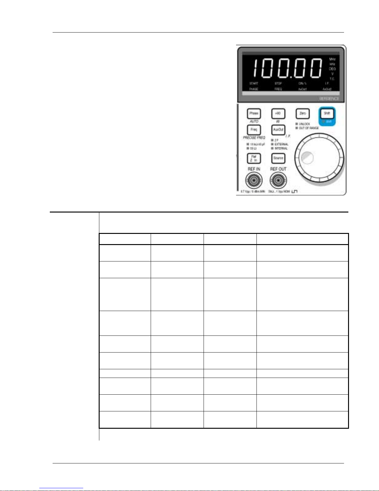
Reference Section
The Reference Section of the front panel contains the Reference
Display, connectors for the External Reference Input and for the
Referenc e Out, and several keys a nd indicators. The knob is also
located here. The display and keys are discus s ed below.
Reference S ect ion 3-27
Reference
Display
The Reference Display is a 4 -½ d igit LED display that shows the following features:
Key Display Knob Adjust? Description
Phase Reference Phase Yes The detection phas e relative to
the refere nce (d e g).
Freq Reference
Frequency
PRECISE
FREQ
I.F. IF Frequency Only in Internal
AuxOut AUX OUT 1, 2 Yes The rear panel Aux Output
CH1/CH2
Offset M o dify
SETTLE... Elapsed Time No Time constants elapsed.
Scan Set Scan Start Yes The start frequency for manual
Scan Set Scan Stop Yes The s top frequency for manual
Scan Set Scan Steps Yes The number of frequency steps
Precise
Reference
Frequency
Offse t Yes The offse t (% f.s . ) fo r t he C H1
Only in Internal
Refere nce Mo de
Only in Internal
Refere nce Mo de
Refere nce Mo de
The detection frequency.
Dis pl a y s the re fe rence
frequency on the Channel 2
and Reference Displays with
extra precision.
The IF (chop frequency) used
in the SR844, provided for
information.
voltages.
or CH2 display qua ntity.
scanning. Note 1
scanning. Note 1
fo r ma nual scanni ng. Note 1
Note 1 See the description of Scan and Rel later in this chapter for more details.
SR844 RF Lock-In Amplifier
Page 86

3-28 Reference Secti on
Freq
PRECISE
FREQ
[Shift–Freq]
This key displays the reference frequency. If the reference mode is EXTERNAL, t he n
the meas ured e xternal reference frequency is dis played. Meas urements are made 6–12
times a second and the display is updated at 5. 7 Hz. The display will be erroneous if the
instrument is UNLOCKed or the frequency is OUT OF RANGE. Indica tors on the front
panel show both of these error conditions. In external reference mode, the kno b s e rves no
function with this dis pla y.
In INTERNAL refere nce mode , the i nternal re fe re nce fre q u e ncy i s d ispla y e d . The
internal reference frequency is adjusted us ing the knob. The SR844 offers 3 digits of
resolution in specifying the internal reference frequency, and 4 digits of accuracy. For
example, frequencies of 1.23 and 1.24 MHz may be selec ted. When 1. 23 MHz is
selecte d, the actual reference frequency will be in the range 1. 229 to 1. 231 MHz.
Use PRECISE FREQ to display the frequency with more resolution (in either reference
mode).
This key sequence shows the reference frequency with 6 or 7 digits of resolution using
the CH2 and Re ference dis pla ys to gether. Read the two displays a s if they were one
single display. The FREQ indicator within the CH2 display turns on whenever the
Precise Frequency is displayed.
To cancel this display mode, choose another reference display (Freq or Phase for
example).
While the internal reference frequency is set to 3 d igits resolu tion, the actual frequency
±
generated in interna l mode may be slightly different (within
1 in the 4th digit).
I.F.
[Shift–
AuxOut]
This key sequence shows the IF frequency on the Reference Display. See Chapter 2,
Sources of Err or , for more information about the IF (chop frequency). This display is
provided as a user convenience. The instrument has weak spurious responses at offsets
of
±2×
IF, ±4×IF, etc. from the reference frequency. Some users may wis h to set up their
experiments to avoid specific IF frequencie s.
When the reference is in internal mode and the IF frequenc y is dis playe d, the knob may
be use d to a djus t the internal reference frequency while showing the IF frequenc y.
Important!
The SR844 covers the operating frequency range in octaves bands. Users can check the
IF frequency to determine whethe r the instrument is a t the high end of an octave band or
the low end of the next band. At the high end of an oc ta ve, the IF frequency will be close
≤
to 3 kHz (12 kHz for time constants
kHz (8 kHz for time constants
≤
300 µs), while at the low end it will be close to 2
300 µs). The IF frequency affects the output update rate
for the a nalog CH1 and CH2 OUTPUTs. T he fastest update rates occ ur at the high end
of each octave band (where the IF is the highest).
AuxOut This key shows the two rear panel Aux output values. Press ing AuxOut alternates
between AUX OUT 1 and AUX OUT 2. The selected output is indicated by AxOut1 or
AxOut2 within the dis pla y. The knob is used to a djust the selec te d outpu t volta ge within
the r ange
±
10.500 Volts.
Phase This key s hows the phase, relativ e to the reference, currently being u s ed for signal
detection. The phase is dis playe d in degrees (–179.99
°
to +180.00°). The knob is used to
adjust the phase. See below for more details.
SR844 RF Lock-In Amplifier
Page 87

The SR844 is calibrated such that an input signal that is in phase with the rising edge of
the External Reference input is measured as having X=R, Y=0 and
Reference Phase is set to 0
°
. If the unit is in Interna l Reference mode, there is no externa l
reference signal; in this case a n input signal in phase with REF OUT yields X=R, Y=0
and
θ=0°
.
The Reference Phas e may be changed to detect the signal at any phas e relative to the
reference. The Reference Phase control is applied inside the DSP (a simple coordinate
rotation), which means that changing the Reference Phase does not change any of the RF,
IF or reference signa ls inside the SR844. The phase control is applied before the output
time-constant filtering.
°
+90
This key adds 90° to the Reference Phase. 360° is subtracted from the phase if necessary
to keep it within range –179.99
°
to +180.00°. This ke y e s s entially exchange s the
measured in-phas e (X) and quadrature (Y) components of the signal.
°
–90°
[Shift– +90°]
This key adds –90
keep it within range –179. 99
to the Reference Phase. 360° is added to the phase if necessary to
°
to +180.00°. This key essentially exchanges the measured
in-phase (X) and quadrature (Y) components of the signal.
Zero This key resets the Reference Phase to 0°.
Reference S ect ion 3-29
θ=0°
when t he
AUTO
[Shift–Phase]
Reference
Mode
Source
2F
[Shift-Source]
This key s equence automatically selects a Reference Phase that matches the phase of the
input signal. This res ults in a measured p hase o f the input signa l that is clo s e to zero.
Note that if the me a s ured phase o f the input signa l is not settle d or is noisy at the time
Shif t-Phase is press e d, the measured phase will not settle to exactly 0
°
.
Auto phase is executed once at the time the keys are pressed. The Reference Phase will
not track changes in the phase of the input signal. Howe ve r the R function a lways
provides the magnitude of the input signal, even as the phase moves , as long as the phase
moves slowly compared to the measurement time cons tant.
In EXTERNAL Reference mode , the SR844 locks to the signal prese nt on the External
Refere nce Input.
In INTERNAL Reference mode, the SR844 gene rates the reference frequency using an
internal synthesizer. It is recommended to leave the External Reference input
disconnected when the unit is in internal mode.
REF OUT
In both reference modes, REF OUT provides a 1 Vpp signal (into 50
Ω
) in phase with the
reference. This signal ca n be used to provide the modula tion necessary in the experiment.
This key sets the Reference mode of the SR844, either EXTERNAL or INTERNAL.
The selected mode is shown by indicators above the key.
This key sequence toggle s 2F harmonic detec tion. 2F mode is shown by the indicator
above the EXTERNAL and INTERNAL indicators.
2F detection is available for both External and Internal Reference modes. In both cases,
the displayed frequency is the 2F detection freque ncy. The frequency of the REF OUT
signa l is a t F or half of the displayed detection frequency. In External mode, the
frequencies of REF IN and REF OUT are both F.
SR844 RF Lock-In Amplifier
Page 88

3-30 Reference Secti on
Important!
The 2F detection frequency is limited to 50 kHz to 200 MHz. This corresponds to a REF
IN and REF OUT frequency range of 25 kHz to 100 MHz.
The absolute phase in 2F mode is not specified. However, the relative phase accuracy
generally applie s .
Ref Z-In
OUT OF
RANGE
UNLOCK
ΩΩΩΩ
This key s elects the impedance of the External Reference Input (REF IN), either 50
10 k
|| 40 pF. The referenc e s ignal should be 0 dBm (sine) or 0.7 Vpp (pulse) for
ΩΩΩΩ
or
proper locking. T he SR844 will lock to othe r amplitudes with possible degradation in
phase accuracy and jitter.
This indicator is on whe never the Externa l Reference input is out of the operating
frequency range (25 kHz to 200 MHz) or is not detected at the input due to insufficient
amplitude or non-periodic pulse shape. This only applies in External Referenc e mode.
This indicator is on whenever the SR844 is not locked.
In External Reference mode, this occurs when the REF IN frequency is changing or
unstable. In Internal Reference mode, this occurs when the internal reference frequency is
changed. The internal synthe s izer requires time to lock to the new frequency.
SR844 RF Lock-In Amplifier
Page 89

Save and Recall 3-31
Save and Recall
Nine setups of the SR844 may be s ave d in non-volatile memory (setup buffers
1-9). The store d s e tups include a ll front panel instrume nt settings, as well as the
remote interface configurations. T he Scan parameters used for manual scans are
sav e d . T he Rel mode d a ta (fre q u e ncie s, configurati ons a nd s to re d Re l v a lu e s)
are not stored. The stored setups do not include any signal history or overload
conditions, nor do they include the internal data buffers .
Save Pressing Save once dis plays SAVE n where n is the last used se tup buffer. A new
setup buffer (1–9) may be se lec ted us ing the knob. The Referenc e dis play s hows YES if
buffer n is in use a nd NO if it is empty.
A second press of the Save key will save the current instrume nt setup in the chosen
setup bu ffer. A co nfirmation me s s a ge SAVE n DONE is displayed briefly.
Any other keypress will abort the save proc ess a nd display the message SAVE NOT
DONE.
Recall Pressing Recall once displays RCAL n where n is the last used se tup buffer. Another
setup buffer (1–9) may be se lec ted us ing the knob. The Referenc e dis play s hows YES if
buffer n is in use a nd NO is it is e mpty.
PRESET
[Shift–Recall]
A second press of the Recall ke y will recall the instrument setup from the chosen setup
buffe r. A conf i rma ti on messa ge RCAL n DONE is displaye d if the recall ope ratio n is
successful. RCAL DATA ERR is displayed if no setup was previously saved in the
selected buffer.
Any other keypress will abort the recall process and display the message RCAL NOT
DONE.
If a remote command is received before the second Recall keypress, the remote
comma nd is proce s s e d normally and the instrument continues to wait for either knob
input or the second Recall keypress.
Important!
• The reca ll ope ration will clear the interna l da ta b uffers (s e e C hapter 4, Data
Storage).
• Recall doe s not affect the stored Rel mode information (see Sca n and Rel later in this
chapter). Thus an instrument configuration may be s ave d at one frequency and
recalled at another frequency, without affecting s tored Rel values.
• Interface setup parameters are not changed.
This key s eq ue nce res tores the instrument to its factory de fau lts (se e ea rlier in this
chapter).
SR844 RF Lock-In Amplifier
Page 90

3-32 Interface
Interface
The SR844 can be interfaced to a host computer via RS232 or GPIB. The keys in
this section configure the interface for proper operation with the host. These
para mete rs mus t b e set before attempting to interface the instrument to the host
computer.
Setup The Setup key cycles through the remote interface configuration parameters. Indicators
above the Setup key indicate whic h parameter is being shown. T he value or setting of
the paramete r is displaye d on the Re ference Display and is adjusted us ing the knob. See
Chapter 4, Introduction, for more information about se tting the c orrec t interface.
Parameter Configuration Notes
GPIB/
RS232
The SR844 outputs data to only one interface at a time. Commands may
be received over both interfaces but responses are directed only to the
selected interface. Use the knob to select either GPIB or R232 for the
output interface.
ADDRESS
BAUD
PARITY
QUEUE
Use the knob to sele ct a G PIB address for the SR844.
Use the knob to sele ct a RS232 baud rate from 300 to 19200 baud.
Use the knob to select EVEN, ODD or NONE for the RS232 pa rity.
The last 256 characters received by the SR844 may be displayed to help
find programming errors. Se tup Qu eu e will displa y 6 hexadecimal
characters at a time (2 each on the Channel 1, Channel 2 and Reference
displays). T urn the knob CC W to move farther back in the buffer and
CW to move towards the most recently received characters. A period ‘.’
is displayed to indicate the ends of the buffer. All characters are
changed to upper-case, spaces are removed, and command delimiters are
changed to linefeeds (0A).
The table below shows the hexa dec imal equivalents of all of the
characters recognized by the SR844.
Hex ASCII Hex ASCII Hex ASCII
0A
2A
2B
2C
2D
2E
30
31
32
33
34
linefeed
*
+
,
–
.
0
1
2
3
4
39
3B
3F
41
42
43
44
45
46
47
48
9
;
?
A
B
C
D
E
F
G
H
4D
4E
4F
50
51
52
53
54
55
56
57
M
N
O
P
Q
R
S
T
U
V
W
SR844 RF Lock-In Amplifier
Page 91

Interface 3-33
35
36
37
38
5
6
7
8
49
4A
4B
4C
I
J
K
58
59
5A
X
Y
Z
L
LOCAL Remote interface commands can put the SR844 into either the Remote state or the Local
Lockout state. It is possible to configure the unit over the remote interface so that the
front pane l is inoperative in these state s . Se e in Chapter 4, Interface Commands , fo r
information on how to do this. Note that the factory preset values are such that the front
panel is not disabled by Remote commands.
Attempts to change the se ttings from the front panel will display the messa ge LOCL
LOUT indicating that local control is locked out by the remote interface.
If the unit is in the Remote state and the front pane l is loc ke d-out, the Local key will
return the unit to the Local state and re-enable the front panel. In the Local Lockout state,
even the Local key is locked o ut. It is not possible to dis tinguish between the Remote
and Local Lockout states from the front pane l indicators, since the REMOTE indicator is
on in both cases. If the Local key does not return the unit to the Local state, the unit is
probably in the Local Lockout state. T here are three wa ys to get out of the Local
Lockout state. One is to turn the power off and back on with the Setup key pres se d; this
restores the factory preset values. The other two methods are by remote commands and
are discussed in greater detail in Chapter 4, Interf ace Commands . LOCL0 ta ke s the unit
out of the Local Lockout state, while OVRM1 e nables the front panel rega rdles s of
Remote or Local Lockout s tate.
REMOT E
SRQ
ACTIVE
ERROR
This indicator shows that the SR844 has been put into either the Remote or Local
Lockout state by receipt of a remote command. Front panel control may not be allowed.
This indicator is on when a GPIB service reque st is generated by the SR844. This
indicator remains o n until a serial poll is co mpleted. See C hapter 4, Status Register
Definitions, fo r more informatio n.
This indicator flashes when there is activity (receive or transmit) on either remote
interface.
This indicator flashes when there is a remote interface error, such as an illegal command,
or a ou t-o f-ra nge para meter.
SR844 RF Lock-In Amplifier
Page 92
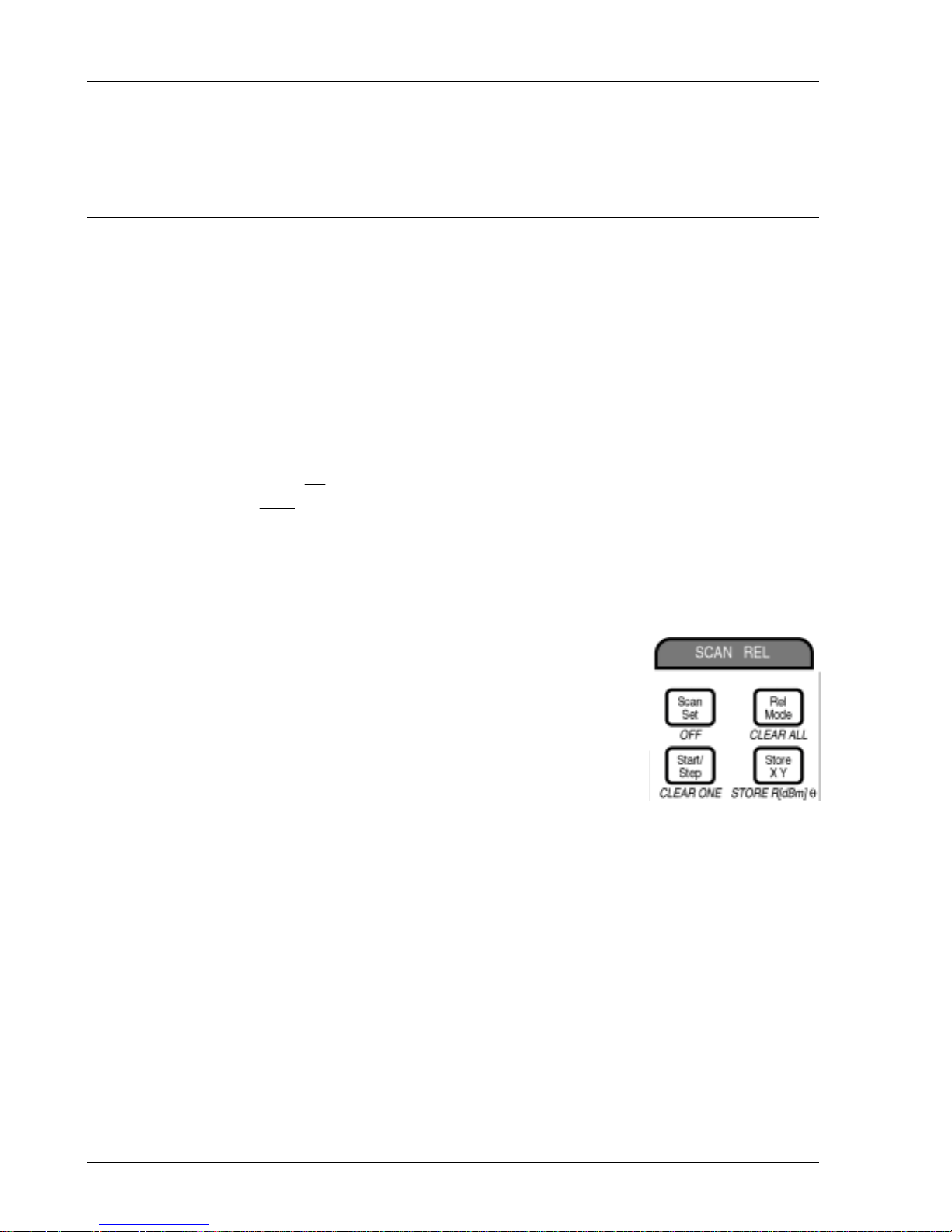
3-34 Scan - Rel
Scan and Rel
Overview
Scans
The SR844 offe rs the facility of doing a manua l frequency scan covering up to 11 frequency points. This
facility is a va ilab le only in the Internal Reference mode. Frequency scans are a convenient method for
making repeated meas urements over a set of frequencies. For example, measurements of device noise or
frequency respons e us ing REF OUT as the signal s ource.
The set of scan frequencies are specified by a start frequency, a stop frequency and the number of points.
The start frequency and s top frequency may be anywhere within the operating range of the instrument,
25 kHz – 200 MHz. The SR844 will se le ct the frequency points by interpolating geometrically between
the start and s top frequencies. T he following equation gives the frequencies F
is the number of points.
i
−1
N
F
FF
=×
istart
stop
F
start
for i=0 to N–1, where N≥2
i
Her e F
start
and F
are the start and stop frequencies respectively. T he geometric interpolation is
stop
appropriate for wide frequency intervals, and is clos e to linear for na rrow frequenc y intervals. The
interpolated frequencies a re rounded to the resolutio n of the inte rnal frequency
source.
The SCAN MODE indicator is on while a scan is in progress. Use the Scan
Set key to setup a s c a n. Scan setup is not permitted while a scan is in progress.
Use the Start/Step key to start a scan and to step through the frequencies. T o
stop a s c a n withou t going through all the frequencies, use OFF (Shift–
Scan Set).
Rels
At each scan frequency, a stored measurement setup, or Rel Configuration
(sensitivity, reserve , etc.), can be recalled . In addition, s tore d offse ts (Rel Values ) may be applie d to the
signal. XY Rel Values are stored X and Y offsets. R
can be stored for each scan frequency.
To store Rel Values at the current s can frequency:
• Use the Store XY key to Auto Offset X and Y and store the offsets as XY Rel offset values. T he
XY REA DY indicator is on when XY Rel Values have been s tored at the current scan frequency. This
also s tores the Rel Configura tion (sensitivity, reserve , etc . ).
θ
Rels are s tored R[dBm] and θ offsets. Rel Values
• Use STORE R[d Bm]θ (Shift–Store XY) to Auto Offset R[dBm] and Auto Phase the reference and
store the results as R[dBm] and
Values have been stored at the current scan frequency. This also stores the Rel Configuration
(sensitivity, reserve , etc.).
SR844 RF Lock-In Amplifier
θ
Rel offset values. The R[dBm]
indicator is on when R[dBm]
θθθθ
θ
Rel
Page 93

Scan - Rel 3-35
Use the Rel Mode key to toggle REL MODE on and off.
In SCAN MODE with REL MODE on, the instrument a utomatically re ca lls the store d Rel Co nfiguration
and Rel Values at each scan frequency. The REL indicator within the CH1 and CH2 displays is on
whenever the recalled Rel Configuration and Rel Values are in effect.
If the current scan frequency does not have a ny stored Rel Values (as indicated by XY READY or
R[dBm]
The stored XY Rel Values are applied as X and Y offsets (adjusted for the current phase). The stored
R[dBm] Rel Value is applied as the R[dBm] offset. The stored
Phase (there is no phase offs et). Offset indicators within the CH1 and CH2 displays are turned on as
appropriate (as well as the REL indicator).
After the Rel Configuration and Rel Values are reca lle d, the instrument setup can be modified using the
front panel or remote interface. Once the configuration is modified, the REL indica tor turns off indicating
that the current configuratio n is not the recalled Rel Configuration. Toggle REL MODE off and back on to
recall the stored Rel Configuration once again.
When REL M ODE is off, stored Rel Configurations and Rel Values are ignored (the c onfiguration and
offsets currently in effect are still applied to the meas urement).
θθθθ)
, the current configuration and offsets remain in effect. The REL indica tor is off in this case.
θ
Rel Value is applied as the Reference
Use the CLEAR ALL key (Shift–Rel Mode) to clear all stored Rel Configurations and Values and
CLEAR ONE (Shift–Start/Step) to clear the Rels at the current scan freque ncy only.
Scan and Rel parameters a re s tored in non-vola tile memory and recalled at power on. They are not stored
with the 9 available stored se tups.
Using Frequency Scans
This section discusses the operation of the frequency Scan Mode. The Scan Mode can be used in
conjunction with Rel Mode as des cribe d in the following section.
Scan Set This key accesses the s can frequency parameters. Successive keypresses are used to
cycle through the Start and Stop frequencies and Number of Points on the Reference
Display. The knob is used at each stage to modify the current parameter.
Changing t he scan p ar amet er s is not permitted if a sc an is in progress (SCA N MODE
indicator on). In such a case the knob has no effect. There are three scan parameters:
Parameter Descri ption
Start The start frequency, F
the START indicator within the dis play . Use the knob to sele ct a s ta rt
frequency in the range 25 kHz – 200 MHz.
Stop The stop frequency F
the STOP indicator within the d is pla y. Use the knob to sele c t a s to p
frequency in the range 25 kHz – 200 MHz.
Number of
Points
The number of points, N, is shown on the Reference Display. There is no
indicator shown in the display. Use the knob to select from 2 to 11 steps .
The number of points include s both the start and stop frequencies, so the
, is shown on the Reference Display, along with
start
, is shown on the Reference Display, along with
stop
SR844 RF Lock-In Amplifier
Page 94

3-36 Scan - Rel
number of interpolated points is N – 2 .
Completing the scan parameter se tup procedure does not start a scan. The frequency
refere nce re mains u nchanged (Internal or External refere nce mode ) a ft e r a ll s c a n
parameters have been set.
Start/Step This key is used to s tep through the s can frequencies. If no sca n has been setup, the
factory preset values are us ed, namely Start = 100 kHz, Stop = 100 MHz, N = 4, which
gives inte rpolated frequencies of 1 MHz and 10 MHz.
The SR844 must be in Internal Refe re nce mode to p e rform a sca n. Start/Step has no
effect unless the unit is in Internal Reference mode.
Successive presses of Start/Step perform the foll owing functions.
Keypress Descripti o n
1st If a scan is not in progress, pressing the Start/Step key will begin one, if
the SR844 is in Internal reference mode. T he frequency is set to the Start
frequency, F
2nd ... Nth Subsequent keypresses step to the next scan frequency, Fi. When the
frequency reaches the Stop frequency, F
turns on.
, and the SCAN M ODE indicator is turned on.
start
,the SCAN DONE indicator
stop
N+1st Another keypress exits the Scan Mode while remaining at the Stop
frequency. The SCAN MODE and SCAN DO NE indicators both turn
off.
N+2nd The ne xt keypress begins another scan, jus t like the 1st keypress a bove.
Important!
During a freque ncy sc a n, changing some front pane l pa rameters will exit Scan Mode.
These are (1) changing the internal frequency and (2) switching to External Reference
mode.
OFF
[Shift–
This key s equence terminates Scan Mode. The SCAN MODE and SCAN DONE
indicators are turned off. It has no effect if SCAN MODE is off.
Scan Set]
Storing and Using Rel Values
This section discusses the storage of Rel Values at the scan frequencies. The Scan and Rel features work
together in a straightforward manner. First, use the Scan keys to specify the frequency scan (Start, Stop
and N) as described previously. T hen, use Start/Step to step through the sc an frequencies while using the
Store keys to store Rel Configurations and Values at each frequency. Changing scan parameters clears all
stored Rels.
XY Rel Values are actually stored X and Y offs ets. R
stored settings of the reference phas e. Rel Values are stored along with the current measurement
configuration. This is because offsets are generally valid only for a specific configuration and are not
SR844 RF Lock-In Amplifier
θ
Rel Values are stored offs ets for R[ dBm] and
Page 95

Scan - Rel 3-37
appropriate for diffe rent configurations. Using stored Rel Values at a scan frequency will also
recall the stored measurement co nfigu ration.
The measurement configuration includes:
• Signal Z-In • Sensitivity
• Wide Reserve • Close Reserve
• Phase (if R
• Ti me Co nstant S lo pe ( bu t no t t he Time Const ant )
Other parameters, suc h as Display, Expand a nd AUX OUT value s a re not included.
Press Rel Mode to turn REL MODE on. In this mode, stored Rel Configurations and Valu es a re
automatically recalled at the current s can frequency (if previously s tored, as indicated by XY READY or
R[dBm]
are turned on. T he XYOffs and ROffs indicators within the displays are turned on and off as a ppropriate.
After a Rel Configuration is recalled, changing the measurement configuration or modifying offsets causes
the REL indicators to turn off. This does not alter the stored Rel Values o r Configuration, it merely
indicates that the current configuration is not the same as the stored configuration. It also does not alter the
offsets currently in use. Use Rel Mode to toggle REL MODE off and back on to recall the stored Rel
Values and Configuration once again.
θ
Rel Values are stored) • Ratio
θθθθ)
. When a Rel Configuration is recalled, the REL indicators within the CH1 and CH2 displays
Changing frequency scan parameters clears all stored Rel Values. Use the CLEAR ALL key (Shift–Rel
Mode) to clear all stored Rel Configurations and Valu es a nd CLEAR ONE (Shift–Start/Step) to clear
the Rels at the current scan frequenc y only.
The Rel Values are saved when the instrument power is turned off. They are not stored with the 9
available stored se tups .
Store XY Performs Auto Offset on both X and Y and stores the XY offsets as XY Rel Values at
the current sc an frequency. X and Y displa ys a nd outputs are offset to zero. Any
previously stored XY Rel Values are replaced. The current measurement configuration is
also save d. Previously stored R
θ
Rel Values are discarded if they were stored with a
measurement configuration which differs from the current one.
The XY READY indic a tor turns on indicating that XY Rel Values a re stored for this
scan frequency.
Store
R[dBm]θ
[Shift–
Store XY]
Performs Auto Phase and Auto Offset on R[dBm] and stores the R[dBm] offset and
reference phas e as R
are offset to zero. Any pre viously s tored R
θ
Rel Values at the current scan frequency. R[dBm] and θ displays
θ
Rel Values are replaced. T he current
measurement configuration is also saved. Previously stored XY Rel Values are
discarded if they were s tored with a measurement configuration which differs from the
current one.
The R[dBm]θθθθ indicator turns on indicating that R
θ
Rel Values are stored for this scan
frequency.
SR844 RF Lock-In Amplifier
Page 96

3-38 Scan - Rel
XY REA DY
R[dBm]θθθθ
Rel Mode
These indicators are on if there are XY or Rθ Rel Values stored for the current scan
frequency. T hey do not imply tha t these Rel Values a re be ing applied to the current
measurement.
This key toggles REL MODE.
In SCAN MODE with REL MODE on, the instrument a utomatically re ca lls the store d
Rel Configura tion and Rel Values at each scan frequency (if previous ly s tored, as
θθθθ)
indicated by XY READY or R[dBm]
. The REL indicator within the CH1 and CH2
displays is on whenever the recalled Rel Configuration and Rel Values are in effect.
If the current scan frequency does not have any stored Rel Values (as indicated by
XY REA DY or R[dBm]
θθθθ)
, the current configuration and offsets remain in effect. The
REL indicator is off in this c a s e .
The stored XY Rel Values are applied as X and Y offsets (adjusted for the current
phase). The stored R[dBm] Rel Value is applied as the R[dBm] offset. The stored
θ
Rel
Value is applied as the Reference Phase (there is no phase offset). Offset indicators
within the CH1 and CH2 displays are turned on as appropria te (a s well as the REL
indicator).
Turning REL MODE off does not change the current measurement. The current
measurement configuration remains in effect. As long as REL MODE is off, stored Rel
Values and Configurations are not recalled at any other scan frequencies.
CLEAR ALL
[Shift–Rel
Mode]
CLEAR O NE
[Shift–Start/
Step]
Any key that
changes the
instrum ent
configuration
Start/Step
This key sequence discards all store d Rel Values and Configurations.
This key sequence discards the s tored Rel Values and Configurations at the current scan
frequency.
All keys in the SIGNAL INPUT and SENSITIVITY sections as well as Slope
Up/Down, Ratio, Recall, Preset, Ref Z-In , Ref Source change the measurement
configu ration and turn the RE L indicators off. This does not affect REL MODE.
This key is us e d to s te p through the scan frequencies. If REL MODE is on, stored Rel
Configurations and Values (if previously s tored) will be app lied.
SR844 RF Lock-In Amplifier
Page 97

Scan - Rel 3-39
Scan and Rel Example
In this example we will make transfer function me a s urements of a devic e– under–tes t, or DUT, using the
SR844 REF OUT signal in Internal Referenc e mode. For this example, we assume that the DUT attenuates
the REF OUT signal. We will make measurements at several freque ncies us ing the Sca n Mode. We will
use Rel Mode to store the meas ured value s when the DUT is by-passed (us ing STO RE R[d Bm]
First, we set the frequency scan parameters to select the scan frequencies. T hen we step through the scan
with the DUT by-passed, storing Rel Configurations and Values at each frequency (using
STORE R[dBm]
through the frequency scan again. This meas ures the transfer response of the DUT directly in dB and
degrees.
If the DUT amplifies the signal, we would need to make the scan with the DUT in the s ignal path first,
storing Rel Values and Configurations. The second scan by-passes the DUT and meas ures the transfer
response (negate both the dB and phase readings). The order is determined by which configuration
(through the DUT or by-pass the DUT) has the larger output signal. This determines the required
measurement configuration at each frequency.
1 Connect the REF OUT signal (appropriately atte nuated and terminated) to the input of the DUT. T he
DUT output should be connec ted to the SIGNAL IN of the SR844.
θ
). This measures the DUT input. Next we pass the signal through the DUT and step
θ
).
Now by-pass the DUT, leave as much of the apparatus in place as possible. It is important to use the
same cabling for both setups (by-pass and through the DUT) in order to preserve phase delays
through the system.
2 Set the frequency scan parameters us ing the Scan Set key and knob as des cribed previously in the
section Using Frequency Scans. Press CLEAR ALL [Shift– Rel Mode] to disca rd any previously
stored Rel Values.
3 Press Start/Step once to begin/continue the frequency scan.
4 Adjust the instrument c onfiguration to measure the signal appropriately. Set the disp lay s to s how
R[dBm] on CH1 and
5
Press STORE R[dBm]θ. This saves the signal phase and the measured value of R[dBm] as well as
the measurement configuration to be used in the next scan.
6 Repeat steps 3–5 until the Scan is done.
7 Now pass the signal thro ugh the DUT.
8 Press Start/Step once more to turn Scan Mode off at the Stop frequency.
9
Press Rel Mode to turn on REL MODE and use the stored Rel Values. The next scan will display
R[dBm] and pha s e rela tive to the original sca n taken with the DUT by-pas sed. T his is exactly the
transfer function we started out to measure.
10 Press Start/Step once to begin/continue the frequency scan.
θ
on CH2. This measures the DUT input.
11 When the measurement is stable, note the readings. In dB and degrees, these give the value of the
transfer function of the DUT at the current frequency.
12 Repeat s teps 10–11 until the Scan is done.
SR844 RF Lock-In Amplifier
Page 98

3-40 Scan - Rel
Rels without Sca n
This sec tion discu s s e s the storage of Rel Values when the unit is not in Scan mode. This is useful for
external reference c o nfiguratio ns or fo r fre q u e ncy p oi nts t hat a re not in a l og series. Up to 1 1 di ffe re nt Rel
Configurations may be stored (at 11 diffe rent frequencies).
To store Rel Values at the current frequency:
• Use the Store XY key to Auto Offset X and Y and store the offsets as XY Rel offset values. T he
XY REA DY indicator is on when XY Rel Values have been s tored at the current frequency. This also
stores the Rel Configuration (sensitivity, reserve, etc.).
• Use STORE R[d Bm]θ (Shift–Store XY) to Auto Offset R[dBm] and Auto Phase the reference and
store the results as R[dBm] and
θ
Rel offset values. The R[dBm]
Values have been stored a t the current frequency. T his als o s tore s the Rel Configuration (s ensitivity,
reserve, etc.).
Use the Rel Mode key to toggle REL MODE on and off.
With REL MODE on, the instrument automatically recalls the s tored Rel C onfiguration and Rel Va lue s
whe never the frequency is within 1% of a frequ ency for which a Rel Configuration and Values has b ee n
stored. The REL indicator within the CH1 and CH2 displays is on whenever the reca lled Rel
Configuration and Rel Values are in effect.
indicator is on when R[dBm]
θθθθ
θ
Rel
If the current fre quency does not have any stored Rel Values (as indicated by XY READ Y or R[dBm]
θθθθ)
the current configuration and offs ets remain in effect. The REL indica tor is off in this case.
The stored XY Rel Values are applied as X and Y offsets (adjusted for the current phase). The stored
R[dBm] Rel Value is applied as the R[dBm] offset. The stored
θ
Rel Value is applied as the Reference
Phase (there is no phase offs et). Offset indicators within the CH1 and CH2 displays are turned on as
appropriate (as well as the REL indicator).
After the Rel Configuration and Rel Values are reca lle d, the instrument setup can be modified using the
front panel or remote interface. Once the configuration is modified, the REL indica tor turns off indicating
that the current configuratio n is not the recalled Rel Configuration. Toggle REL MODE off and back on to
recall the stored Rel Configuration once again.
When REL M ODE is off, stored Rel Configurations and Rel Values are ignored (the c onfiguration and
offsets currently in effect are still applied to the meas urement).
• Pressing CLEAR ALL clears all s tored Rel Configurations, both those stored with a scan and those
stored at s pecific frequencies.
• Pressing the CLEAR ONE clears the Rel Configuration s to red with the current freque ncy (if any).
• The Rel Configurations are indexed by frequency with a 1% tolerance band. Rels stored at 90.0MHz
will be recalled whe never the fre quency falls between 89.1MHz (-1%) and 90. 9MHz (+1%).
,
• You should familiarize yourse lf with the preceding sections before using the Rels without Scan.
SR844 RF Lock-In Amplifier
Page 99

Auto Functions
Auto Functions 3-41
Wide
Reserve
Close
Reserve
Sensitivity Shif t–
Shif t–
WideResrv
Down
Shif t–
CloseResrv
SensUp
Select the Wideband Dynamic Reserve mode auto matically. This function
will execute once when the keys a re press ed. A tone sounds when the
function is complete. T he rese rve will not continu e to c hange even if the
input signal c hanges substa ntially. T o adju s t for the change d co nditions, it
may be neces sary to perform the Auto function again, or make manual
changes. The Wide Reserve AUTO indicator is on while this function
executes.
Select the Clos e D ynamic Reserve mode automatically. This function will
execute once when the keys are pres s ed. A tone sounds when the function is
complete. T he rese rve will not continu e to change even if the input signal
changes s u bs ta ntially. T o ad jus t for the change d c onditions, it may be
necessary to perform the Auto function again, or make manual changes. The
Sensitivity AUTO indicator is on while this function executes.
Automatically adjus t the se nsitivity ba s ed on the detected s ignal magnitude,
instrument reserve se ttings and overload conditions. This function executes
once when the keys are press e d. A tone sounds when the function is
complete. T he se nsitivity will not continue to change even if there is a
substa ntial change in the input signa l. In the ca s e of a s u bs ta ntial signal
change, it may be neces s a ry to perform the Auto Sensitivity function a gain,
or adjust the se nsitivity/res erve manually. Auto Se nsitivity take s more time
to complete at larger time constants. The Sensitivity AUTO indicator is on
while Au to Sensitivity is in progress.
Auto Sensitivity will not execute if the time constant is greater
than 1 s.
Phase Sh ift–Phase Select the Reference Phase that matches the phase of the input signal. A tone
sounds when the function is complete. This res ults in a measured phase of
the input signal that is close to zero. If the measured phase of the input
signal is not settled or is noisy at the time Shift-Phase is presse d, the
Offset CH1 or CH2
Offset Auto
measured phase may not settle to 0
Auto phase is executed once at the time the keys are pressed. The Reference
Phase will not track changes in the phase of the inp ut s ignal. However the R
function always provides the magnitude of the input signal, even as the
phase moves, as long as the phase moves slowly compared to the
measurement time cons tant.
This key s ets the Offset for the displaye d qua ntity equal to the negative of
its current value, so that the display , with offset app lied, is eq ua l to zero.
The Offset is turned On if it is not already On. This key has no effect for
quantities that may not be offset.
Important!
If the display is X or Y, Auto Offset is performed on both X and Y and turns
on both X and Y offsets. This is true e ve n if the othe r dis pla y is not
displaying X or Y at the time.
°
.
SR844 RF Lock-In Amplifier
Page 100

3-42 Shift Functions
Shift Functions
Some keys have shift functions labeled in blue below the key.
SETTLE... Shift–Time
Constant Up
PRESET Shift–Recall This key sequence restores the instrument to its factory defaults (see
–90° [Shift– +90°] This key s equence changes the reference phase by –90°.
I.F. [Shift– AuxOut] T his key se quence shows the IF frequenc y on the Re ference Display.
This key s equence causes the Reference Display to show the elapsed
time (in units of the current Time Constant).
earlier in this chapter).
See Chapter 2, Source s of Error , for more information about the IF
(chop frequency). This display is provided as a use r convenienc e.
The instrument has weak spurious responses at offsets of
±4×
IF, etc. from the refe re nce fre q ue ncy . So me users may wish to set
up their experiments to avoid specific IF frequencie s .
Whe n the reference is in internal mode and the IF frequency is
displayed, the knob may be used to adjus t the internal reference
frequency while showing the IF frequency.
Important!
The SR844 covers the operating frequency range in octave bands.
Users can check the IF frequency to determine whether the instrument
is at the high end of an octave band or the low end of the next band.
At the high end of an octave, the IF frequency will be clos e to 3 kHz
≤
(12 kHz for time cons tants
close to 2 kHz (8 kHz for time constants
affects the output update rate for the analog CH1/CH2 OUTPUT s .
The fastest update rates occ ur at the high end of each octave band
(where the IF i s the highest ) .
300 µs), while at the low end it will be
≤
300 µs). The IF frequency
±2×
IF,
PRECISE
FREQ
Null [Shift–Shift] A second keypres s cancels the first Shift if it is pres s e d b y mistake .
OFF [Shift–
CLEAR ALL [Sh ift–Re l
[Shift– Freq] T his key seque nce shows the reference frequency with 6 or 7 digits
Scan Set]
Mode]
SR844 RF Lock-In Amplifier
resolution using the C H2 and Reference displays to gether. Read the
two displays a s if they were one single dis p lay . While the inte rnal
reference frequency is s et to 3 digits res olution, the actual frequency
generated in interna l mode may be slightly different (within
4th digit).
To cancel this display mode, choose another reference display (Freq
or Phase for example).
This key s equence terminates Scan Mode. It has no effect if SCAN
MODE is off.
This key sequence discards all store d Rel Co nfigurations a nd Values.
±
1 in the
 Loading...