


MODEL SR570
Low-Noise Current Preamplifier
Phone: (408) 744-9040 • Fax: (408) 744-9049
email: infor@thinkSRS.com • www.thinkSRS.com
1290-D Reamwood Avenue
Sunnyvale, California 94089
Copyright © 1997 by SRS, Inc.
All Rights Reserved.
Revision 1.6
(03/2005)


SR570 Low-Noise Current Preamplifier
Table of Contents
Condensed Information
Safety and Use iii
Accessories Furnished iv
Environmental Conditions iv
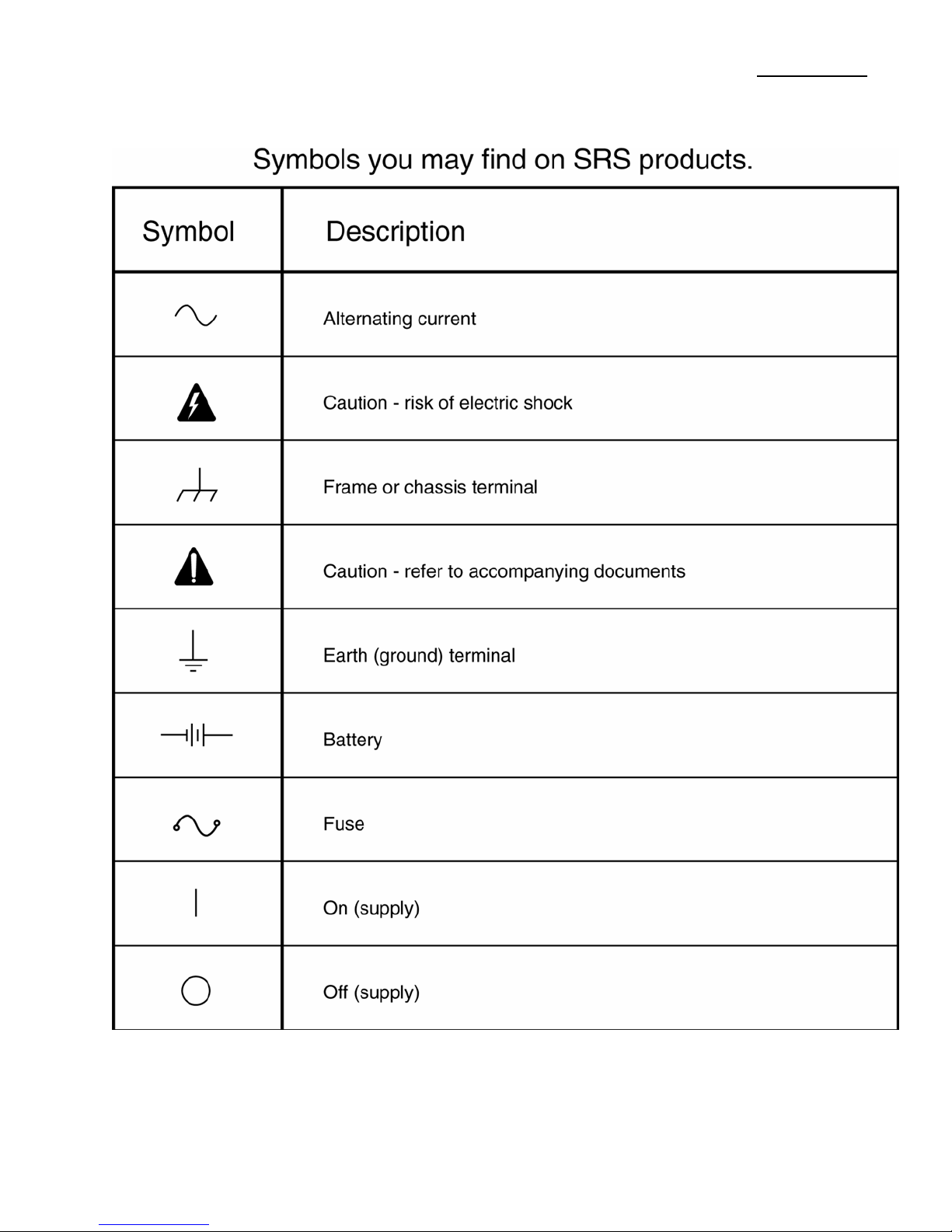
Symbols v
Specifications vi
Verifying Specifications ix
Abridged Command List x
Operation and Controls
Introduction 1
Overview 1
Quick Start Instructions 1
SR570 Block Diagram 2
Front Panel Operation 3
Power 3
Input 3
Defaults 3
Bias Voltage 4
Input Offset Current 4
Invert 4
Filters 4
Gain Mode 5
Sensitivity 5
Output 5
Filter Reset 5
Status 6
Rear Panel Operation 7
AC Power Input 7
Amplifier Power Output 7
Battery Charger 7
Blanking Input 8
Toggling Input 8
RS-232 Interface 8
Battery Care and Usage 8
Recharging 8
Battery Care 8
Programming
Remote Programming 10
Introduction 10
Command Syntax 10
Detailed Command List 10
Sensitivity Control 10
Input Offset Current Control 10
Bias Voltage Control 11
Filter Control 11
Other Commands 11
Programming Examples 12
BASIC 12
Microsoft C 13
SR570 Circuitry
Circuit Description 14
Front-End 14
Filters and Gain 14
Output Stages 14
Overload Detection 15
Microprocessor 15
Battery Charger and Preregs 15
Power Regulators 16
Rear Panel Interfaces 16
Batteries and P.E.M. 16
Front Panel 16
Calibration & Repair 17
Calibration 17
Front-end Replacement 17
Battery Replacement 17
Fuse Replacement 17
Appendices
A. Amplifier Noise Sources
Input Noise A-1
Noise Sources A-1
Johnson Noise A-1
Shot Noise A-1
i

SR570 Low-Noise Current Preamplifier
1/f Noise A-1
Total Noise A-2
External Noise Sources A-2
Capacitive Coupling A-2
Inductive Coupling A-2
Ground Loops A-3
Microphonics A-3
Thermocouple Effects A-3
Baluns A-4
B. Gain Allocation
Front-end Amplifier B-1
Op Amp Allocation B-1
Dynamic Reserve B-1
C. Capacitance Effects
Feedback Capacitance C-1
Input Capacitance C-1
Component Parts List D-1
Main Circuit PC Board D-1
Front & Rear Panel PC Boards D-11
Miscellaneous Parts D-15
Schematic Circuit Diagrams Sheet No.
Input Stage 1/10
Filter and Gain 1 2/10
Filter and Gain 2 3/10
Output Stage 4/10
Microprocessor Section 5/10
Digital I/O & Front Panel Control 6/10
Battery Charger & Preregulators 7/10
Power Regs & Rear Panel Conn. 8/10
Front Panel 9/10
Rear Panel 10/10
ii

SR570 Low-Noise Current Preamplifier
Safety and Preparation for Use
WARNING: Dangerous voltages, capable of causing death, are present in this instrument. Use
extreme caution whenever the instrument covers are removed.
************ CAUTION ************
This instrument may be damaged if operated
with the LINE VOLTAGE SELECTOR set for
the wrong ac line voltage or if the wrong fuse is
installed.
LINE VOLTAGE SELECTION
When the AC power cord is connected to the unit
and plugged into an AC outlet, the unit
automatically switches the amplifier power source
from internal battery operation to line operation.
The internal batteries are charged as long as AC
power is connected.
The SR570 operates from a 100V, 120V, 220V, or
240V nominal AC power source having a line
frequency of 50 or 60 Hz. Before connecting the
power cord to a power source, verify that the
LINE VOLTAGE SELECTOR card, located in the
rear panel fuse holder, is set so that the correct AC
input voltage value is visible.
Conversion to other AC input voltages requires a
change in the fuse holder voltage card position and
fuse value. Disconnect the power cord, open the
fuse holder cover door and rotate the fuse-pull
lever to remove the fuse. Remove the small
printed circuit board and select the operating
voltage by orienting the printed circuit board so
the desired voltage is visible. Push the card firmly
into its slot. Rotate the fuse-pull lever back to its
normal position and insert the correct fuse into the
fuse holder.
LINE FUSE
Verify that the correct line fuse is installed before
connecting the line cord. For 100V/120V, use a
1 Amp fuse and for 220V/240V, use a 1/2 Amp
fuse.
LINE CORD
The SR570 has a detachable, three-wire power
cord for connection to an AC power source and to
a protective ground. The exposed metal parts of
the instrument are connected to the outlet ground
to protect against electrical shock. Always use an
outlet which has a properly connected protective
ground.
CONNECTION TO OTHER INSTRUMENTS
All front panel BNC shields are isolated from the
chassis ground and the power outlet ground via a
1MΩ resistor. Do not apply any voltage to either
the shields or to the outputs. The outputs are not
protected against connection to any potential other
than circuit ground.
VENTILATION
Always ensure adequate ventilation when
operating the SR570. The unit will generate heat
while charging batteries.
POWER-UP
All instrument settings are stored in nonvolatile
memory (battery backed-up RAM) and are
retained when the power is turned off. They are
not affected by the removal of the line cord. If the
power-on self test passes, the unit will return the
settings that were in effect when the power was
last turned off. If an error is detected or if the
backup battery is exhausted, the default settings
will be used. Additionally, if the FILTER RESET
key is held down when the power is turned on, the
instrument settings will be set to the defaults
shown below:
Sensitivity = 1 µA/V, calibrated
Invert = off
Input Offset = +1 pA, calibrated, off
Bias = 0 V, off
Filters = none
Hi Pass Freq = 0.03 Hz
Lo Pass Freq = 1 MHz
Gain Mode = Low Noise
iii

SR570 Low-Noise Current Preamplifier
REPACKAGING FOR SHIPMENT
The original packing materials should be saved for
reshipment of the SR570. If the original packing
materials are not available, wrap the instrument in
polyethylene sheeting or equivalent and place in a
strong box, cushioning it on all sides by at least
three inches of high-density foam or other filler
material.
USE IN BIOMEDICAL APPLICATIONS
Under certain conditions, the SR570 may prove to
be unsafe for applications involving human
subjects. Incorrect grounding, component failure,
and excessive common-mode input voltages are
examples of conditions in which the instrument
may expose the subject to large input currents.
Therefore, Stanford Research Systems does not
recommend or approve the SR570 for such
applications.
WARNING REGARDING USE WITH
PHOTOMULTIPLIERS
The front-end amplifier of this instrument is easily
damaged if a photomultiplier is used improperly
with the amplifier. When left completely
unterminated, a cable connected to a PMT can
charge to several hundred volts in a relatively
short time. If this cable is connected to the inputs
of the SR570, the stored charge may damage the
front-end op amps. To avoid this problem, always
connect the PMT output to the SR570 input before
turning the PMT on.
ACCESSORIES FURNISHED
- Power Cable
- Operating Manual
ENVIRONMENTAL CONDITIONS
OPERATING
Temperature: 10° C to 40° C
Relative Humidity: < 90% Non-condensing
NON-OPERATING
Temperature: -25° C to +65° C Non-condensing
WARNING REGARDING BATTERY
MAINTENANCE.
Batteries used in this instrument are sealed lead
acid batteries. With usage and time these batteries
can leak. Always use and store this instrument in
the feet-down position. To prevent possible
damage to the circuitboard, it is recommended that
the batteries be periodically inspected for any
signs of leakage.
iv
Specifications
v

Specifications
Input
Input Virtual null or user set bias voltage (-5V to +5V).
Input Impedance See Table 1
Input Offset ±1 pA to ±5 mA full scale adjustable dc offset current.
Maximum Input ±5 mA.
Noise See graphs on next page.
Sensitivity 1 pA/V to 1 mA/V in a 1-2-5 sequence. Vernier sensitivity in 1%
steps.
Frequency Response Flat to ±0.5 dB up to 1 MHz (1 mA/V sensitivity ). Frequency response
can be adjusted from the front panel to compensate for the effects of
source capacitance at the input.
Grounding Amplifier ground is fully floating. Amplifier and chassis grounds may be
connected together at rear panel banana plug connectors.
Filters
Signal Filters Two configurable (low or high pass) filters: 6 or 12 dB/octave. The -3 dB
point of each filter is settable in a 1-3-10 sequence from 0.03 Hz to 1 MHz
for lowpass filters and 0.03 Hz to 10 kHz for highpass filters.
Filter Reset Long time constant filters may be reset with a front panel button.
Gain Allocation
Low Noise Most of the gain is allocated in the front end of the instrument to decrease
the magnitude of Johnson noise at the output.
High Bandwidth Front-end gain is reduced to increase the amplifier’s frequency response.
Low Drift A very low input bias current amplifier is used for more accurate
measurements on the higher sensitivity ranges.
Output
Gain Accuracy ±(0.5 % of output + 10 mV [50 mV High BW]) @ 25°C [100 pA/V - 1
mA/V sensitivities]
DC Drift See Table 1
Maximum Output ±5 V into a high impedance load (50W output impedance).
Slew Rate Limit 2 V peak to peak at 1 MHz.
Rear Panel ±12 VDC @200 mA, referenced to amplifier ground.
Interface
RS-232 Listen only, 9600 Baud DCE, 8 bit, no parity, 2 stop bits. All instrument
functions may be controlled. PC compatible serial connector. Optically
isolated.
External Gating TTL inputs to set gain to zero (blanking) or to invert gain polarity
(toggling).
General
Operating Temperatures 0 to 50° C
Power 100, 120, 220 or 240 VAC, 50/60 Hz from line. Internal batteries provide
up to 15 hours between charges. Batteries are charged while connected to
the line. Line power required is 30 watts while batteries are charging and 6
watts once fully charged.
Dimensions 8.3" x 3.5" x 13.0". Rack mounting hardware available.
Weight 15 lbs. (including batteries).
Warranty 1 year.
vi
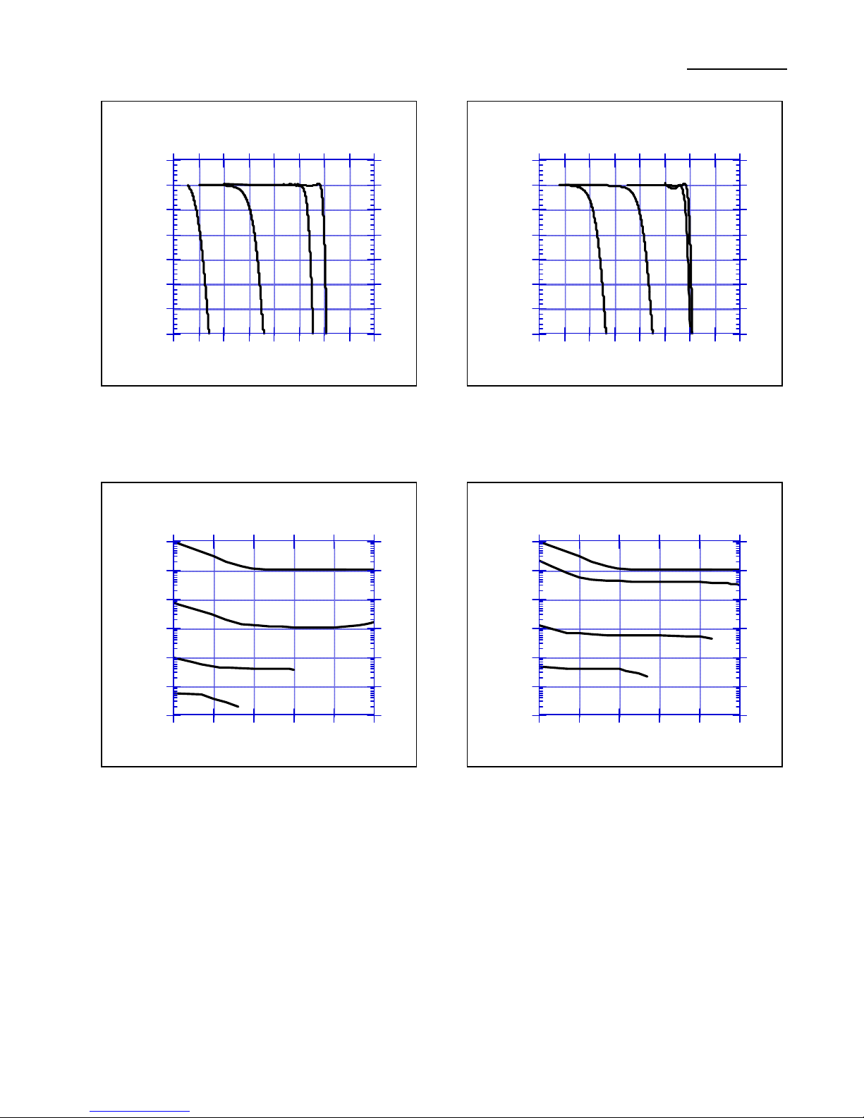
Specifications
Low Noise Mode
High Bandwidth Mode
1
0
-1
-2
1
0
-1
-2
-3
-4
Gain / Nominal Gain (dB)
-5
1 nA/V
100 nA/V
10 µA/V
1 mA/V
-3
-4
Gain / Nominal Gain (dB)
-5
1 nA/V
100 nA/V
10 µA/V
1 mA/V
-6
1 100 10
4
Frequency (Hz)
6
10
8
10
-6
1 100 10
4
Frequency (Hz)
6
10
8
10
Amplifier Bandwidth for several sensitivity settings (typical).
Low Noise Mode
High Bandwidth Mode
-9
10
-11
10
-13
10
Current Noise (Amps/¦Hz)
-15
10
1 10 100 1000 10
1 nA/V
Frequency (Hz)
100 nA/V
1 mA/V
10 µA/V
4
5
10
-9
10
-11
10
-13
10
Current Noise (Amps/¦Hz)
-15
10
110
1 nA/V
Frequency (Hz)
1 mA/V
10 µA/V
100 nA/V
100 1000 10
4
5
10
Current Noise as a function of Frequency for several sensitivity settings (typical).
Note: The amplifier bandwidth and noise data were taken with the front panel frequency compensation
adjusted for flat frequency response over the widest frequency range, with an input capacitance of
100 pF. Either the bandwidth or the noise specification can be improved at the expense of response
flatness.
vii
Specifications
Table 1
Temperature Coefficient
Bandwidth (3 dB) 1 Noise/√Hz
Sensitivity (A/V)
High BW Low Noise Low Noise High BW ±(%input + offset) /°C Impedance
10-3 1.0 MHz 1.0 MHz 150 pA 150 pA 0.01 % + 20 nA 1 Ω
10-4 1.0 MHz 500 kHz 60 pA 100 pA 0.01 % + 2 nA 1 Ω
10-5 800 kHz 200 kHz 2 pA 60 pA 0.01 % + 200 pA 100 Ω
10-6 200 kHz 20 kHz 600 fA 2 pA 0.01 % + 20 pA 100 Ω
10-7 20 kHz 2 kHz 100 fA 600 fA 0.01 % + 2 pA 10 kΩ
10-8 2 kHz 200 Hz 60 fA 100 fA 0.01 % + 400 fA 10 kΩ
10-9 200 Hz 15 Hz 10 fA 60 fA 0.025 % + 40 fA 1 MΩ
10-10 100 Hz 10 Hz 5 fA 10 fA 0.025 % + 20 fA 1 MΩ
10-11 20 Hz 10 Hz 5 fA 10 fA 0.040 % + 20 fA 1 MΩ
10-12 10 Hz 10 Hz 5 fA 5 fA 0.040 % + 20 fA 1 MΩ
1
Frequency Compensation adjusted for flat frequency response (typical values).
2
Average noise in the freq. range below the 3 dB point but above the frequency where 1/f noise is significant.
Note: The values listed above are typical for a 100 pF source capacitance and an infinite source resistance.
Significantly higher values of source capacitance or finite source resistance can degrade these specifications.
Proper use of the “FREQ COMP” adjustment and signal filters allows the user to alter the rated noise or
bandwidth values. The LOW DRIFT mode has a much lower bandwidth than the LOW NOISE and HIGH
BW modes, and should only be used for low frequency measurements.
2
Low Drift (11 ° - 28 °C) DC Input
viii

Specifications
Verifying Specifications
To verify the specifications given for the
SR570 current amplifier, a few
straightforward procedures should be
followed. First, the unit must be warmed up
for about 60 minutes. Second, for best
performance, the input current should produce
an output voltage of about 1 V or less. This
eliminates problems with slew rate limiting in
the various amplifier stages. Finally, care must
be taken in selection of a current source for
any measurement. Since an ideal current
source has infinite impedance, any source
used for measurements should have an
impedance greater than the inverse of the
sensitivity in ohms. Most specifications listed
above were measured with an input
capacitance of 100 pF. Higher input
capacitance will lead to a decrease in
performance.
Lets look at a simple example to illustrate
some of these principles. To test the gain and
frequency response of the instrument at 1
nA/V sensitivity, we might use a 1 V RMS
sine wave across a 1 GΩ resistor and through
1 meter of coax cable into the amplifier frontend. The cable itself has about 100 pF of input
capacitance to ground. Any other sources of
capacitance will only increase this value, and
degrade the noise performance of the
instrument. The 1 GΩ resistor, while a good
current source at DC, will be less accurate at
higher frequencies due to capacitance of the
resistor. A typical resistor will have about 0.1
pF capacitance, which will provide a parallel
impedance of 1 GΩ at about 1.6 kHz. Since
this effect provides an alternate path for
current, the actual current to the amplifier will
be increased and may be misinterpreted as a
peaking in the frequency response of the
amplifier near 1 kHz. These are only a few
examples of what can go wrong when making
a measurement. It is very important that the
current source be completely characterized
before performing specification verification.
Keep in mind the following items when trying
to verify specifications or when making
sensitive measurements:
1. Make sure the source impedance is greater
than the inverse of the sensitivity (e.g.
with a sensitivity of 1 nA/V use a source
impedance greater than 1 GΩ).
2. If using a voltage source and a big resistor
to source the current, use several smaller
resistors in series instead of one larger
value to reduce the shunting capacitance.
3. Adjust the FREQ COMP pot on the front
panel to optimize frequency response for
the source character- istics and for the
sensitivity selected.
4. Use short lengths of high quality coaxial
cable to connect to the amplifier input.
5. Keep the amplifier output below 1 VRMS
to avoid slew rate limiting at high
frequencies.
6. Ground the chassis (green connector on
back) but do not connect the chassis to the
amplifier ground (white connector).
7. For low level measurements, disconnect
the power cord and use the internal
batteries.
ix

Abridged RS-232 Command List
Command Syntax
All RS232 commands consist of four letter codes, followed in most cases, by an integer value (n). Commands
must end with a carriage return and linefeed <CR><LF>.
The SR570 RS232 interface is configured as listen only, 9600 baud DCE, 8 data bits, no parity, 2 stop bits,
and is optically isolated to prevent any noise or grounding problems.
Sensitivity control commands
SENS n Sets the sensitivity of the amplifier. n ranges from 0 (1 pA/V) to 27 (1 mA/V).
SUCM n Sets the sensitivity cal mode. 0 = cal, 1 = uncal.
SUCV n Sets the uncalibrated sensitivity vernier. [0
Input Offset Current control commands
IOON n Turns the input offset current on (n=1) or off (n=0).
IOLV n Sets the calibrated input offset current level. n ranges from 0 (1 pA) to 29 (5 mA).
IOSN n Sets the input offset current sign. 0 = neg, 1 = pos.
IOUC n Sets the input offset cal mode. 0 = cal, 1 = uncal.
IOUV n Sets the uncalibrated input offset vernier. [-1000
Bias Voltage control commands
BSON n Turns the bias voltage on (n=1) or off (n=0).
BSLV n Sets the bias voltage level in the range. [-5000
Filter control commands
FLTT n Sets the filter type. 0=6 HP, 1=12 HP, 2=6 BP, 3=6 LP, 4=12 LP, and 5=none.
LFRQ n Sets the value of the lowpass filter 3dB point. n ranges from 0 (0.03Hz) to 15 (1 MHz).
HFRQ n Sets the value of the highpass filter 3dB point. n ranges from 0 (0.03Hz) to 11 (10 kHz).
ROLD Resets the filter capacitors to clear an overload condition.
Other commands
GNMD n Sets the gain mode of the amplifier. 0=low noise, 1=high bw, 2=low drift.
INVT n Sets the signal invert sense. 0=non-inverted, 1=inverted.
BLNK n Blanks the front end output of the amplifier. 0=no blank, 1=blank.
*RST Resets the amplifier to the default settings.
≤ n ≤ 100] (percent of full scale).
≤ n ≤ +1000] (0 - ±100.0% of full scale).
≤ n ≤ +5000] (-5.000 V to +5.000 V).
x

Operation and Controls
INTRODUCTION
Why use a Current Amplifier?
Many people wonder why current amplifiers are
necessary. Why not simply terminate a current
source with a resistor and amplify the resulting
voltage with a voltage preamplifier? The answer
is twofold. First, to get a large voltage from a
small current, large resistors are necessary. In
combination with cable capacitance and other
stray capacitance, this can lead to unacceptable
penalties in frequency response and phase
accuracy. Current amplifiers have much better
amplitude and phase accuracy in the presence of
stray capacitance. Secondly, using resistive
terminations forces the current source to operate
into possibly large bias voltages–a situation that
is unacceptable for many sources and detectors.
Current amplifiers can sink current directly into
a virtual null, or to a selected DC bias voltage.
Overview
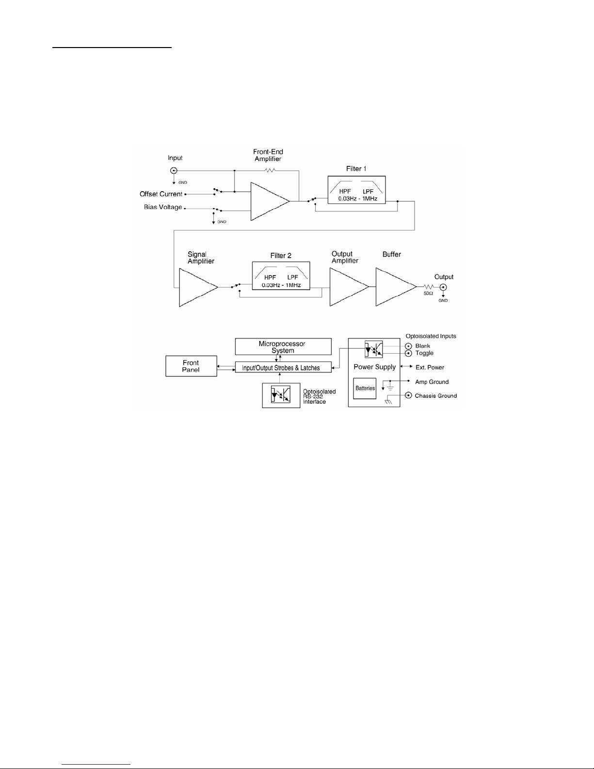
The SR570 is a low-noise current preamplifier,
providing a voltage output proportional to the
input current. Sensitivities range from 1 mA/V
down to 1 pA/V. The general architecture is
diagrammed in figure 1 on the following page.
The DC voltage at the input can be set as a
virtual null or biased from -5V to +5V. An input
offset current from 1pA to 1 mA may also be
introduced. The user can choose between low
noise, high bandwidth, and low drift settings,
and can invert the output relative to the input.
Two configurable R-C filters are provided to
selectively condition signals in the frequency
range from DC to 1 MHz.
The SR570 normally operates with a fully
floating ground with the amplifier ground
isolated from the chassis and the AC power
supply. Input blanking, output toggling and
listen-only RS-232 interface lines are provided
for remote instrument control. These lines are
optically isolated to reduce signal interference.
Digital noise is eliminated by shutting down the
processor clock when not executing a frontpanel button press or an RS-232 command.
Internal sealed lead-acid batteries provide up to
15 hours of line-independent operation. Rear
panel banana jacks provide access to the internal
regulated power supplies (or batteries) for use as a
voltage source.
Use this procedure as a quick orientation to the
instrument's features and capabilities. If you
encounter problems, read the detailed discussions
on operation.
1) Make sure that the correct line voltage has been
selected on the rear panel power entry module.
2) With the unit's power switch "OFF", hold the
"FILTER RESET" key down and turn the unit
"ON". This will return all instrument settings to their
default state.
3) Select a filter from the "FILTER TYPE" menu.
Then use the up/down arrows of the "FILTER
FREQ" menu to choose the filter 3 dB points.
4) If an input offset current is desired, choose a
current level from the "INPUT OFFSET" menu with
the up/down arrow keys. The current will be applied
when the "ON" led is lit.
5) When the bias voltage is off, the amplifier input
is a virtual null. To set a bias voltage, use the
up/down arrow keys of the "BIAS VOLTAGE"
menu. The test point will always reflect the selected
bias voltage, but the bias will only be applied when
the "ON" led is lit.
6) Set the sensitivity and gain mode to the desired
settings for the the amplitude of the signal to be
measured.
7) Adjust the "FREQ COMP" pot near the input
BNC to compensate the amplifier's frequency
response for any input capacitance. An external
square wave signal from the source under test can be
used for precise calibration.
8) Connect the signal to be measured to the
"INPUT" BNC. The signal will be converted to a
voltage, filtered and amplified. The amplifier output
voltage can be accessed from the "OUTPUT" BNC
connector.
1
Operation and Controls
Figure 1: SR570 Block Diagram
2
Operation and Controls
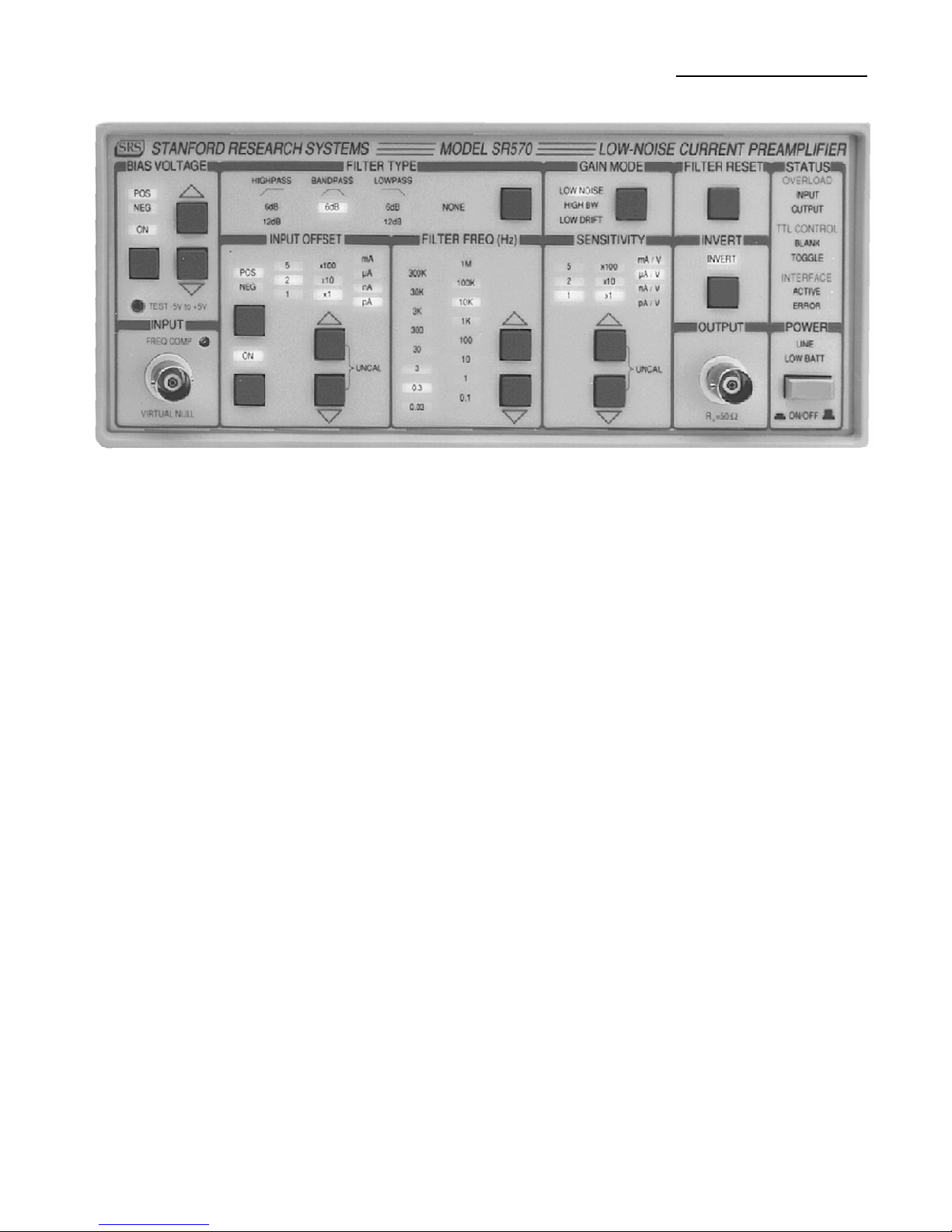
Figure 2: SR570 Front Panel
FRONT PANEL OPERATING SUMMARY
The operation of the SR570 Low-Noise
Preamplifier has been designed to be as simple
and intuitive as possible. The effect of each
keypress on the front panel is reflected in the
change of a nearby LED. All front panel
functions, except power, can be controlled
through the rear-panel RS-232 interface.
Power
The SR570 is turned on by depressing the
POWER switch. When disconnected from AC
power, the unit will operate for approximately
15 hours on internal sealed lead-acid batteries.
Up to 200 mA of unregulated battery power is
available at the rear panel banana jacks as long
as the power switch is in the ON position.
Battery life will be reduced when the unit is
providing external power through the rear panel
jacks. When operating on batteries, the front
panel LINE indicator will not be lit. As the
batteries near depletion, the LOW BATT LED
will light, indicating that the unit should be
connected to AC power to charge the batteries.
When connected to an AC power source,
amplifier power is derived from regulated line
power, and the internal batteries are
automatically charged. When operating on AC
power, the front panel LINE indicator is on to
indicate the source of amplifier power.
Charging status is indicated on the rear panel by the
CHARGE and MAINTAIN LED indicators.
Input
An insulated BNC is provided to connect the signal
of interest to the amplifier. Care should be taken in
choosing a cable to connect to the amplifier input.
Both cable capacitance and dielectric quality will
affect sensitive measurements. Whenever possible,
use low noise coaxial cable and always use the
shortest possible cable length. Above the input BNC
is the FREQ COMP adjustment potentiometer. This
feature allows the user to compensate for any input
capacitance by varying the capacitance across the
front-end amplifier feedback resistor. In this way,
the amplifier bandwidth can be easily adjusted to
compensate for source capacitance by measuring a
square wave signal from the source of interest and
using FREQ COMP to optimize the output
waveform. See Appendix C for further discussion of
the effects of source capacitance.
Defaults
Any changes made to the front panel settings of the
SR570 will be stored even when power is turned off,
as long as the batteries are hooked up. To reset the
SR570 to its default settings, simply turn the power
off, and while depressing the FILTER RESET
button, turn the power on. Alternatively, removing
3

Operation and Controls
the batteries from an SR570 with no AC power
connected will reset the unit to the default state.
The default settings are:
Sensitivity = 1 µA/V, calibrated
Invert = off
Input Offset = +1 pA, calibrated, off
Bias = 0 V, off
Filters = none
Hi Freq = 0.03 Hz
Lo Freq = 1 MHz
Gain Mode = Low Noise
Bias Voltage
In the default configuration, the SR570 is a
virtual null at the input BNC. The bias voltage
provides a variable -5V to +5V voltage (12 bit,
1.22 mV resolution) at the input. This voltage
can be used to bias a photodiode or similar
device. The voltage level is set by the up/down
arrows in the bias voltage section of the front
panel. The up arrow increases the voltage
towards +5V, and the down arrow decreases the
voltage towards -5V. To enable the bias voltage,
simply push the button directly below the bias
ON LED. The selected voltage can be monitored
at the TEST point with a DC voltmeter whether
the bias voltage is turned on or not.
Input Offset Current
The SR570 can provide a DC current offset to
suppress any background currents at the input.
The offset range can be changed from 1 pA to 5
mA (both positive and negative) in discrete
increments. Use the up/down arrow keys in the
Input Offset section to change the current level.
In addition to these fixed settings, the user may
specify arbitrary currents through the UNCAL
feature. To set an uncalibrated offset current, the
user must press both up and down buttons
simultaneously, lighting the UNCAL LED. In
this mode, by pressing the up or down
pushbuttons, the user may reduce the calibrated
current in roughly 0.1% increments from 100%
down to 0% of the selected offset value. In
contrast to other front-panel functions, when in
UNCAL the instrument's key-repeat rate will
start slowly and increase to a limit as long as
either button is depressed. Simultaneously
pressing both Offset buttons once again will
restore the unit to the previously calibrated current
setting, and turn off the UNCAL LED. The sign of
the current is set with the button directly below the
POS and NEG LEDs. A positive offset current is
defined to be a current that will produce a positive
output voltage with no signal connected to the input
BNC and INVERT not selected. The button below
the input offset ON LED turns the offset on and off.
The current level can be adjusted whether the offset
current is turned on or not.
Invert
The INVERT pushbutton allows the user to invert
the output of the instrument with respect to the
input. A positive current will give a negative voltage
and visa versa. The INVERT LED displays the
output sense relative to the input unless the
TOGGLE feature is being used.
Filters
The SR570 contains two identical 1st-order R-C
filters whose cutoff frequencies and configuration
(high-pass or low-pass) are controlled from the front
panel. The maximum bandwidth of the instrument is
1 MHz.
The FILTER CUTOFFS can be configured in the
following six ways:
i. high-pass filter at +6 dB / octave
ii. high-pass filter at +12 dB / octave iii.
high-pass filter at +6 dB / octave, and
low-pass filter at -6 dB / octave (band pass)
iv. low-pass filter at -6 dB / octave
v. low-pass filter at -12 dB / octave
vi. no filters in the signal path
Filter settings are chosen by the FILTER TYPE
pushbutton. Each time the FILTER TYPE
pushbutton is pressed, the instrument configures the
two R-C filters in the progression shown above.
LEDs give a visual indication of the filter
configuration.
The filter cutoff frequencies are controlled by the
up/down arrows in the FILTER FREQ section.
When the FILTER TYPE section is configured
solely as high-pass or low-pass (i, ii, iv and v ), the
cutoff frequency is illuminated by one of sixteen
4

Operation and Controls
LEDs in the range from 0.03 Hz to 1 MHz. High
pass filters are not available for the four highest
frequency settings. When the filter section is
configured as band-pass (iii), the cutoff
frequencies are illuminated by two LEDs. The
lower frequency setting marks the cutoff for the
high-pass filter, and the higher setting is the
cutoff for the low-pass filter.
To change the values of the bandpass cutoff
frequencies, use the up arrow button to change
the lowpass cutoff and the down arrow to
change the highpass cutoff. If the displayed
frequency is already at the highest or lowest
possible choice, then pushing the button again
will cause the frequency to “wrap around” to the
opposite extreme frequency. In this case the two
cutoffs can be set to the same frequency to
provide a narrow bandpass. The highpass
frequency can never exceed the lowpass
frequency. When both filters are removed from
the signal path (vi) all FREQ LEDs are
extinguished and the NONE LED is lit.
Gain Mode
The allocation of gain throughout the instrument
is set using the GAIN MODE pushbutton. The
gain mode feature controls the tradeoffs between
dynamic reserve, bandwidth, and noise in the
amplifier circuits. The Gain Mode is displayed
by three indicator LEDs: LOW NOISE, HIGH
BW, and LOW DRIFT. For a given gain setting,
the LOW NOISE mode allocates gain toward
the front-end in order to quickly "lift" low-level
signals above the instrument's noise floor. The
LOW DRIFT mode allocates the gain just as the
LOW NOISE mode, except the front-end op
amp is switched to one with a very low input
bias current for high sensitivity settings. The
HIGH BW setting allocates more gain toward
the output stages after the filters. Since smaller
values of feedback resistance are needed for the
front-end gain, the bandwidth of the amplifier is
increased over that of the other two settings.
This also prevents signals which are attenuated
by the filters from overloading the amplifier. See
Appendix B for further details of op amp
selection for the different gain modes.
Sensitivity
The instrument's sensitivity is increased or decreased
using the SENSITIVITY section pushbuttons.
Sensitivity settings from 1 pA/V to 1 mA/V are
available and are displayed as the product of a factor
1, 2 or 5 and a multiplier (x1, x10, x100) with the
appropriate units. In addition to these fixed settings,
the user may specify arbitrary sensitivities through
the UNCAL feature.
To set an uncalibrated or arbitrary sensitivity, the
user must press both up and down buttons
simultaneously, lighting the UNCAL LED. In this
mode, by pressing the up or down pushbuttons, the
user may reduce the calibrated sensitivity in roughly
1% increments from 100% down to 0% of the
selected sensitivity. In contrast to other front-panel
functions, when in UNCAL, the instrument's keyrepeat rate will start slowly and increase to a limit as
long as either sensitivity button is depressed.
Simultaneously pressing both sensitivity buttons
again will restore the unit to the previously
calibrated sensitivity setting, and turn off the
UNCAL LED.
Output
The output of the instrument is an insulated BNC
with a 50 ohm output impedance. In most
applications, the instrument will be used to drive
high impedance loads (e.g. voltmeters or
oscilloscopes). Therefore, the instrument's gain is
calibrated for high impedance loads. When driving
a 50 ohm load, the gain of the amplifier is reduced
by a factor of two. The shields of the two front-panel
BNCs are connected together and form the
amplifier's floating ground. In addition, a balun is
used at the output to reduce common mode noise.
See the end of Appendix A for more details about
the output balun.
Filter Reset
If an overload occurs with filter settings of long time
constants, the FILTER RESET pushbutton will
speed the SR570's recovery from overload. The
filters will be discharged by momentarily grounding
the filter capacitors.
The FILTER RESET button is also used to return
the unit to its default settings. Simply hold down the
5
 Loading...