

Page 1

Model SR554
Transformer Preamplifier
email: info@thinkSRS.com • www.thinkSRS.com
1290-D Reamwood Avenue
Sunnyvale, Califor nia 94089
Phone: (408) 744- 9040 • Fax: (408) 744- 9049
Copyright © 1999 by SRS, I nc.
All Rights Re s e r v e d .
Revision 1.2 (10/2001)
Page 2

Page 3

SR554 SPECIFICATIONS
Input s Single ended or differential
Input Impedance 0.5 Ω
Maximum Inputs Transformer and Buffer: 14.0 mV RMS (±20 mV peak)
Transformer only: 350 mV RMS (±0.5 V peak)
Common Mode Range: ± 100 VDC
Rejection: 140 dB @ 100 Hz
Isolation > 40dB DC to 500 MHz
Input Noise 120 pV/√Hz @ 10 Hz (typical)
(Transformer and Buffer) 100 pV/√Hz @ 100 Hz
100 pV/√Hz @ 1000 Hz
(see noise contours, pg. 5)
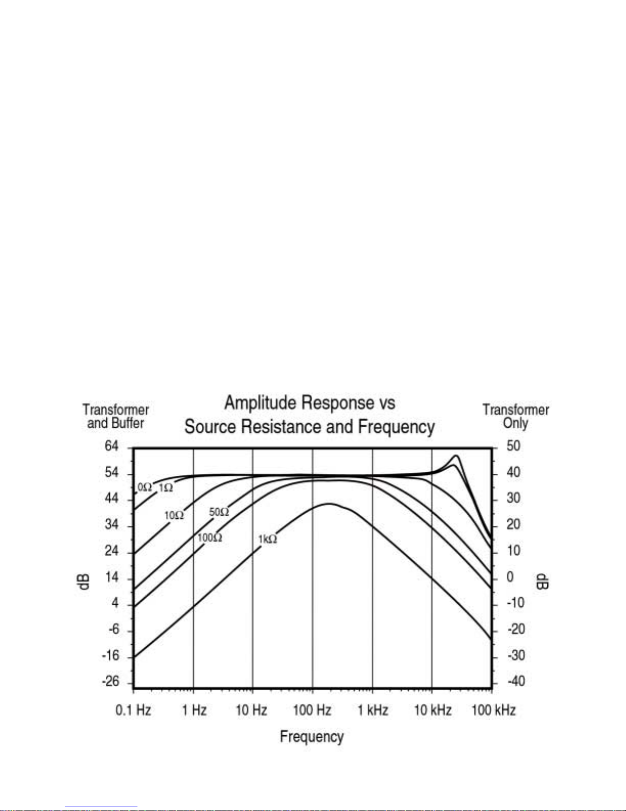
Gain Transformer and Buffer: 500 (nominal)
Transformer only : 100 (nomi nal)
See Amplitude-Frequency Response Curve (pg 6).
Gain Accuracy 5% (with fixed source resistance)
Gain Stability 100 ppm/ °C
Outputs Single ended or differential
Output Impedance Transformer and Buffer: < 1.0 Ω
Transformer only: > 5000 Ω
Maximum Output Transformer and Buffer: 7.1 V RMS (10 Volts peak)
Transformer only: 35.3 V RMS (50 Volts peak)
Power Provided by any SRS lock-in amplifier via the supplied
connector cable or from a ± 20 volts DC @ 100 mA source.
Mechanical 2.9" X 3.8" X 7.5" (HxWxL), 4 lb.
Warranty One year parts and labor on materials and workmanship.
1
Page 4

2
Page 5
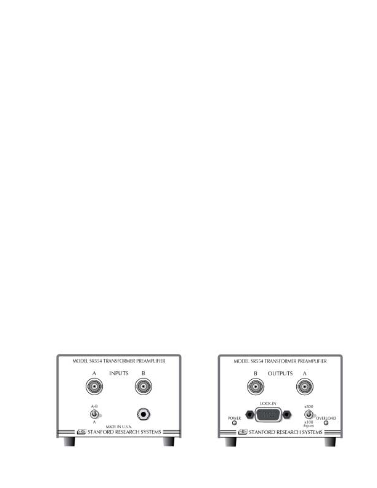
OPERATION
The SR554 Transformer Preamplifier is
desig ned to be used with al l SRS Lock-in
amplifiers. It can reduce input noise of a
lock-in amplifier dramatically (as low as
100 pV/√Hz) and e xte nds the lock-in’s f ul l
scale sensitivity (without expand). It also
nearly elimi nates noi se radiated bac k f ro m
the lock-in amplifier to the users
experiment. When used as a remote
preamplif ier, t he SR554 ca n elimi nate t he
effects of noise pickup on long signal
cables. The SR554 transformer is
designed to be used with its internal
buffer, but the buffer may be by passe d fo r
transformer only operation. When used
as a simple transformer, no power
connection is required.
CONNECTING THE SR554
When the transformer and buff er are used
together, power is s upp lied to the SR554
via the 9 pin connector and cable. This
cable mates with all SRS lock-in amplifiers
through the rear panel connector. To use
the SR554 without an SRS lock-in, the
user must provide their own ±20 VDC
(100 mA) source. Always connect the
power ca ble to t he SR554 while t he loc kin power is off. Attach one end of the
cable to the connecto r on the rear o f the
SR554, and connect the other e nd to t he
PRE-AMP connector on the rear of the
lock-in. If a longer cable is required, any
standard 9 pin cable will s uff ice since al l
connections are straight through. When
the lock-in power is on, the POWER
indicator on the SR554 will light.
The SR554 outp ut s witc h se lects bet ween
buffered mode with a gain of 500,
(transformer and buffer) or bypassed
mode with a gain of 100 (transformer
alone). In the buffered mode, the
transformer secondary goes into a low
noise buffer which drives the output cable.
This is to reduce loading due to the
transformer output impedance (about 5
kΩ) and c ab le c apaci tance (10's o f pf). If
the user prefers not to use the b uffer o r if
power is n’t avai lable f or the pre amp, t hen
the SR554 ca n be used i n the bypassed
mode. I n the bypass ed mo de, the outp ut
impedance of the pre-amp is 5 kΩ and
care must be taken to avoid loading the
output with too much cable capacitance.
Power should not be connected to the
SR554 when used in the bypass mode.
INPUT CONNECTION
Signals into the SR554 c an be co nnected
either single ended through t he (A ) input,
or differentially through the (A-B) inputs.
In the single ended configuration the
shield and center conductor of the (A)
input are connected to the transformer.
For differential connection, the shields of
the input BNC’s are connected to the
SR554 case and the (A) and (B) center
conductors connect to the transformer.
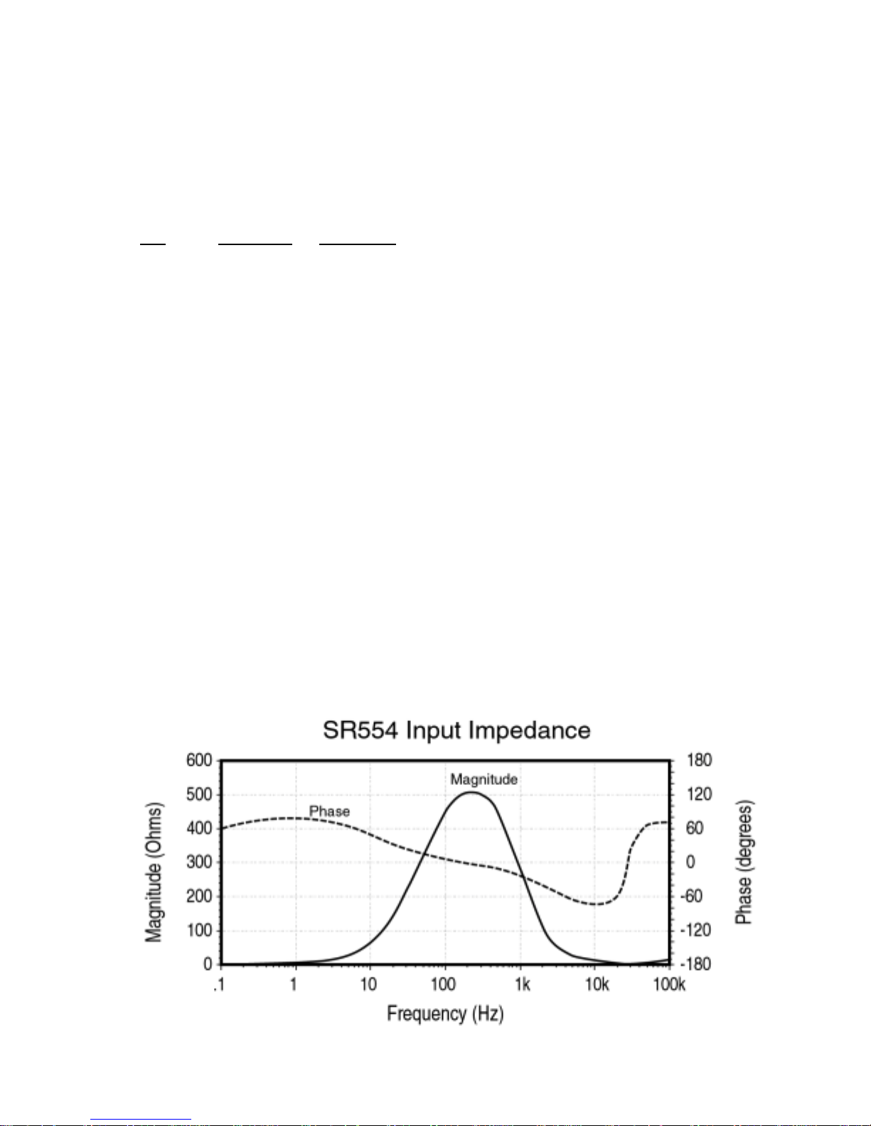
The input i mpedance is a combination of
0.5 Ω and 0.5 H (i n se ries) i n para llel wit h
3
Page 6
1.6 µF. The real portion of the input
impedance (0.5 Ω) determines the noise
performance. See page 7 for detailed
information on input impedance.
The input c an be f loated up t o ±100 VD C
with respect to the chassis. The
maxim um AC i nput bef ore overload is 14
mV RM S (±20 mV peak) whe n the unit i s
in the b uffered mo de. I n eit her mo de, t he
input is clamped at about 350 mV RMS
(±0.5 V peak). Care should be taken when
the unit is used in the bypassed mode,
since a ±0.5 V pea k i np ut becomes ±50 V
at the output.
In the buffered mode, the OVERLOAD
indicator will light when the preamplifier
overloads. An overload that occur after
the preamplifier will be indicated by the
lock-in amplifier’s overload indicator. The
SR554’s overload indicator is only
functional when the unit is in the buffered
mode. If the unit is operated in the
bypassed mo de a nd po wer is app lied, t he
overload LED may light even when the
unit is not overloaded. This does not
indicate an overload, but is due to leakage
current of the buffer amplifier and its
protectio n circuit ry. To avoid thi s, power
should not be co nnected when the unit is
used in the bypassed mode.
OUTPUT CONNECTION
For single ended operat io n the (A) O utp ut
of the SR554 s hould be co nnected to the
(A) Input of the lock-in amplifier. The
center conductor carries the signal and
the shield is ground. For most
applicati ons, this si ngle co nnectio n will be
adequate.
For situations with potential noise pick-up
on the cable, it may be better to operate in
the differential mode. In differential
4
Page 7
operation the (A) and (B) center
conductors carry the signal and shielded
preamp ground, and the shields are tied to
the SR554 chassis. The (A) and (B)
cables should be twisted together to
prevent inductive pick-up.
For most experiments it is preferable to
use the SR554 in the buffered mode. If
the preamplifier is used in the bypass
mode, care m ust be ta ken to not lo ad the
output. The output resistance of the
transformer is at least 5 kΩ (for a 0 Ω
source) and is typically 10,000 times the
input resistance. Therefore, a 50 Ω
source impeda nce wi ll beco me 50 0 kΩ. If
the instrument that the SR554 is
connecte d to has an i np ut impeda nc e o f 1
MΩ, 1/3 of the signal is lost. Any
signifi cant cabl e capacit ance will create a
low-pass filter with this o utput resistance
as well, so short cables should always be
used.
GAIN OF SR554
The actual gain o f the SR554 i s a function
of the source impedance, frequency and
the set gain. In the bypass mo de (x100) ,
the gain will be affec ted by loadi ng on t he
output. T he gai n is f ai r ly flat o ver a ra nge
of input impedances (<10 Ω) and
frequencies (5 Hz-10 kHz). The actual
gain can be determined from the
amplitude-frequency response curves on
page 4. The plot assumes operating the
SR554 in the buffered mode or with no
loading on the output in the bypassed
mode.
5
Page 8

EXTRA LOW NOISE MEASUREMENTS
When making extremely low noise
measurements, it is a good practice to
connect t he gro unding p lug o f the SR554
to a ground point near t he e x perim e nt. If a
good ground is not available near the
experime nt, co nnect a wi re fro m the lo ckin chassis (using a lug under one of the
chassis screws) to the grounding lug of
the SR554.
USING THE SR554 WITH SRS LOCKINS
The SR554 is not sensed through the 9
pin cable by SRS lock-in amplifiers.
Therefore the lock-in does NOT
compensate for the gain of the preamp.
Measurements made using the preamp
must be divided by t he gai n of the SR554.
The actua l gain ca n be obt ained fro m t he
amplitude response curves on page 4.
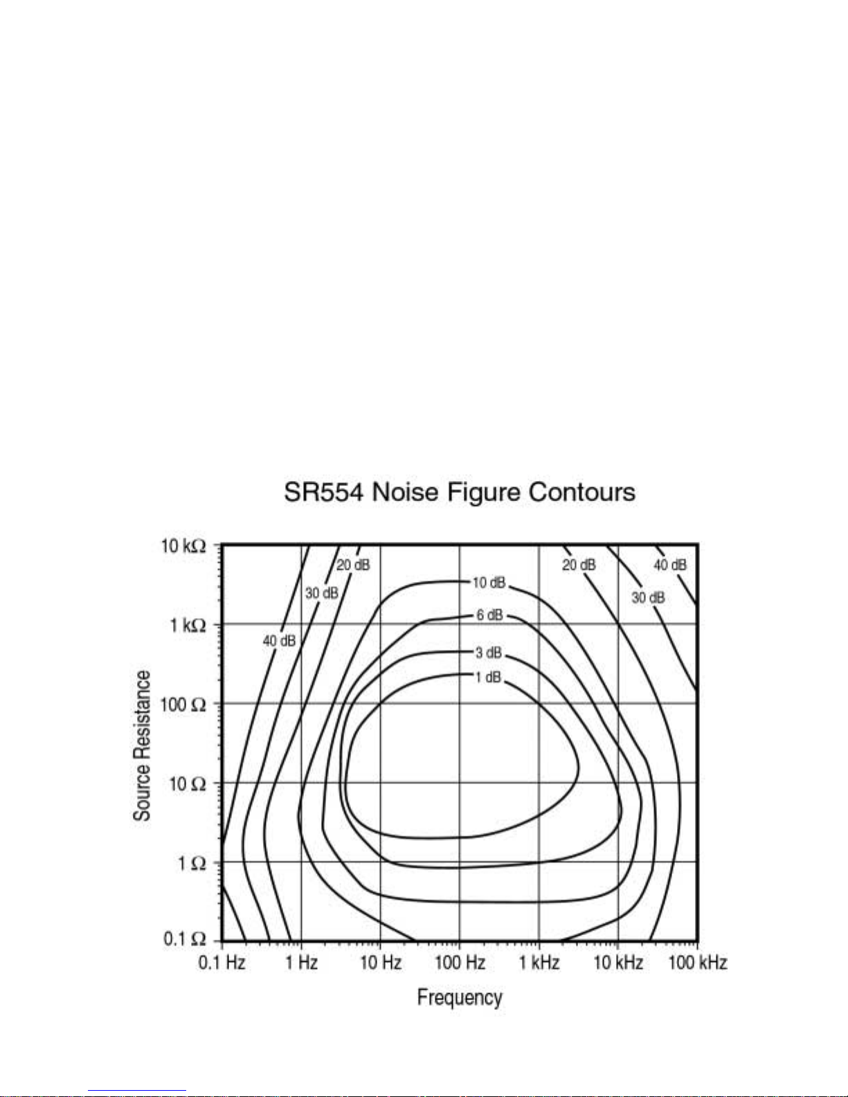
NOISE FIGURE
The noise figure describes the noise
contribution of an amplifier in a
measureme nt when compa red to a n ideal
amplifier.
The expressi on:
where N is t he measured noise, A is the
pre-amp gain and enrs
is the Johnson
noise of the source imp edance, des cribes
the noise figure contours shown below.
The optimum ope rating freq uency can be
determined from this graph.
USING THE SR554 WITH THE
SR810/830/850
For typical measurements the lock-in input
should be set to AC coupled, with the
shield grounded. For low frequency
measurements (<1Hz), set the lock-in to
DC coupled, with the shield grounded,
since the SR554 can sens e signals below
the lock-in’s AC coupling frequency
(0.16 Hz).
USING THE SR554 WITH THE
SR510/530
The SR510/530 is AC coupled from 0.5
Hz to 100 kHz. M easurem ents be low 0.5
Hz are not recommended with the
SR510/530.
6
Page 9
USING THE SR554 WITHOUT AN SRS
LOCK-IN
The SR554 can be powered with an
external power supply. Power is applied
through the 9 pin co nnecto r as described
below.
PIN VOLTAGE
CURRENT
1 +20 V 100 mA
6 -20 V 100 mA
7,8 Ground
Bo th voltages are requi red. Pi ns 7 and 8
should be tied toget her a nd grounded. A l l
other pins should be le ft open.
COMMON MODE REJECTION RATIO
The SR554 has an extreme ly high C MRR
at low freq uencies ( up to 16 0 dB be low 10
Hz). It drops off at higher frequencies due
to capacitive coupling between the
primary and secondary windings and
reduced signal gain. See the graph below
for the relationship between CMRR and
frequency.
ground po int. If a ground i s not avai lable
near the experiment, connect a wire to the
lock-in using a lug under one of the
chassis screws.
INPUT IMPEDANCE
The input impedance of the SR554
appears as a combination of 0.5 Ω and
0.5 H (in series) in parallel with 1.6 µF an d
several parasitic impedances. The
transformer primary has a DC resistance
of 0.2 Ω and a primary inductance of 0.5
H. The secondary has a DC resistance of
3 kΩ a nd a c apacitanc e of about 160 pF.
When the secondary impedance is
converte d over to the primary sid e of the
transf ormer by t he t urns ratio (1:1 00), the
0.5 Ω, 0.5 H and 1.6 µF values are
obtained. The actual values of the
magnitude and phase of the input
impedance is shown in the graph below.
RADIATED NOISE
The SR554 reduces radiated noise from
the lock- in amplifier’s input by 40 dB
(100x) over most freque ncies (DC to 500
MHz ). To minimize radi a ted noi se, a t hi c k
(low impedance) wire should be
connecte d f ro m the gro und p l ug to a q uiet
7
Page 10

8
Page 11

PERFORMANCE TESTS
Performance tests are designed to verify
that the unit is performing within the
specifications.
Necessary Equipment:
1. Lock - In Amp lif ie r Freq
Range 0.1 Hz - 100 kHz
Output Ampl 4 mV rms - 1 Vrms
Output Z 50 Ω
Recommended SRS
SR850/830/810
2. 50 ΩΩΩΩTerminator
3. 50 ΩΩΩΩ, 20 dB Attenuator
The instructions here apply to SRS DSP
lock-ins (SR850/830/810). Other lock-in
amplifiers may be used. However they will
require substantially longer time constants
to arrive at accurate measurements.
1) Connect the 9-pin power cable from
the rear of the lock-in amplifier to the
SR554. Connect the 20 dB attenuator
to the lock-in reference output and a
BNC cable from that to the SR554
(A) input. Connect an other BNC cable
from the SR554's (A) output to the
lock-in’s (A) input. Set SR554 to
buffered mode (X500), (A) input.
2) Power on the lock-in in the default
condition. (SR810/830 Power on
Setup, SR850 Power on Bksp) This
places the loc k-i n i n a known stat e.
The power LED of the SR554 should
light.
4) F or each frequency, the following
amplitude should be observed, ± 5%.
Frequency Amplitude
1.0 Hz 31 mV
10 Hz 252 mV
100 Hz 438 mV
200 Hz 442 mV
500 Hz 439 mV
1 kHz 414 mV
10 kHz 96 mV
100 kHz 11 mV
5) Disconnect the loc k-in refe re nce from
the SR554 input. Connect the 50 Ω
terminator to the SR554 (A) input.
6) Set the lock-in to measure noise.
7) F or each frequency and time constant,
the following rms noise voltage should
be observed (±10%). Set the lock-in
sensitivity to about 5 times the
expected reading and allow it to settle
(10-20 time constants) before making
readings.
Frequency Time Constant
Noise
Voltage
1.0 Hz 3.0 s 480 nV
10 Hz 1.0 s 260 nV
100 Hz 0.1 s 460 nV
200 Hz 0.1 s 460 nV
500 Hz 0.1 s 460 nV
1 kHz 0.03 s 420 nV
10 kHz 0.03 s 120 nV
100 kHz 0.03 s 60 nV
3) Set the input to DC coupled, grounded
shield. Set the time constant to 300
ms (1 s for 1 Hz measurement), 12
dB/oct filter and turn on synchronous
filtering (if available). Set the display
type to magnitude (R) and the
reference sinewave amplitude to 10
mV rms.
9
Page 12

10
Page 13

Part List
Ref. SRS part Value Description
C 101 5-00254-501 130P Capacitor, Ceramic Disc, 50V, 10% , SL
C 102 5-00023-529 . 1U Cap, Monolythic Ceramic, 50V, 20%, Z5U
C 103 5-00023-529 . 1U Cap, Monolythic Ceramic, 50V, 20%, Z5U
C 104 5-00005-501 150P Capacitor, Ceramic Disc, 50V, 10% , SL
C 105 5-00023-529 . 1U Cap, Monolythic Ceramic, 50V, 20%, Z5U
C 106 5-00312-503 . 005U Capacitor, Ceramic Disc, 50V, 20% , Z5U
C 107 5-00016-501 470P Capacitor, Ceramic Disc, 50V, 10% , SL
C 108 5-00044-509 47U Capacitor, Electr olyt ic, 50V, 20% , Rad
C 109 5-00100-517 2. 2U Capacitor, Tantal um, 35V, 20% , Rad
C 110 5-00100-517 2. 2U Capacitor, Tantal um, 35V, 20% , Rad
C 111 5-00023-529 . 1U Cap, Monolythic Ceramic, 50V, 20%, Z5U
C 112 5-00312-503 . 005U Capacitor, Ceramic Disc, 50V, 20% , Z5U
C 113 5-00016-501 470P Capacitor, Ceramic Disc, 50V, 10% , SL
C 114 5-00044-509 47U Capacitor, Electr olyt ic, 50V, 20% , Rad
C 115 5-00100-517 2. 2U Capacitor, Tantal um, 35V, 20% , Rad
C 116 5-00281-521 220U Capacitor, Elect r olyt ic, 25V, 20% , Rad
C 117 5-00281-521 220U Capacitor, Elect r olyt ic, 25V, 20% , Rad
D 101 3-00226-301 1N5822 Diode
D 102 3-00226-301 1N5822 Diode
D 103 3-00403-301 1N459A Diode
D 104 3-00403-301 1N459A Diode
D 105 3-00011-303 RED LED, T1 Package
D 106 3-00010-303 G REE N LED, T1 Package
J 101 1-00003-120 B NC Connector, BNC
J 102 1-00003-120 B NC Connector, BNC
J 103 1-00003-120 B NC Connector, BNC
J 104 1-00003-120 B NC Connector, BNC
J 104 1-00014-160 9 PI N D Connector, D-Sub, Right A ngle PC, Female
J 109 1-00229-102 BINDING Binding Post
L 101 6-00174-630 6611 TYPE 43 Ferrite Beads
L 102 6-00174-630 6611 TYPE 43 Ferrite Beads
PC1 7- 00613- 701 SR554 PREAMP Printed Circ uit Board
R 101 4-00141-407 100 Resistor, M etal Film, 1/8W, 1%, 50PPM
R 102 4-00188-407 4.99K Resistor, M et al Film, 1/8W, 1%, 50PPM
R 103 4-00134-407 1.24K Resistor, M et al Film, 1/8W, 1%, 50PPM
R 104 4-00138-407 10.0K Resistor, M et al Film, 1/8W, 1%, 50PPM
R 105 4-00142-407 100K Resistor, M et al Film, 1/8W, 1%, 50PPM
R 106 4-00166-407 200K Resistor, M et al Film, 1/8W, 1%, 50PPM
R 107 4-00166-407 200K Resistor, M et al Film, 1/8W, 1%, 50PPM
R 108 4-00142-407 100K Resistor, M et al Film, 1/8W, 1%, 50PPM
R 110 4-00063-401 3. 0K Resist or , Carbon Film, 1/4W , 5%
R 111 4-00045-401 2. 0K Resist or , Carbon Film, 1/4W , 5%
R 112 4-00056-401 22 Resistor, Car bon Film, 1/4W, 5%
R 113 4-00056-401 22 Resistor, Car bon Film, 1/4W, 5%
R 114 4-00056-401 22 Resistor, Car bon Film, 1/4W, 5%
SW101 2-00022-217 DPDT Switch, On-None-O n, Toggle, Right A ngle
SW102 2-00027-214 DPDT Switch, Miniature Bat Toggle
T 101 6-00169-610 SR554 Transformer
T 102 6-00173-614 T68- 17 Iron Powder Core
T 103 6-00173-614 T68- 17 Iron Powder Core
U 101 3-00535-340 AD743 Integrated Circuit ( Thr u-hole Pkg)
U 102 3-00193-340 LM 339 Integrated Circuit ( Thr u-hole Pkg)
U 103 3-00118-325 78L15 Transistor , TO-92 Package
U 104 3-00124-325 79L15 Transistor , TO-92 Package
Z 0 0-00025-005 3/ 8" Lugs
11
Page 14

Part List
Ref. SRS part Value Description
Z 0 0-00043-011 4- 40 KEP Nut, Kep
Z 0 0-00079-031 4- 40X3/ 16 M / F Standoff
Z 0 0-00089-033 4" Tie
Z 0 0-00128-053 4" #24 Wire #24 UL1007 Strip 1/4x1/4 Ti n
Z 0 0-00150-026 4- 40X1/ 4PF Screw, Black, All Types
Z 0 0-00187-021 4- 40X1/ 4PP Scr ew, Panhead Phillips
Z 0 0-00208-020 4- 40X3/ 8PF Screw, Flat head Phillips
Z 0 0-00209-021 4- 40X3/ 8PP Scr ew, Panhead Phillips
Z 0 0-00221-000 SR440FOO T Hardware, Misc.
Z 0 0-00263-052 3" #22 W ire #22 UL1007
Z 0 0-00266-052 8- 1/ 2" #22 BLK Wire #22 UL1007
Z 0 0-00304-043 7/ 8X3/ 8X1/ 16 Washer, nylon
Z 0 0-00386-003 SO LDR SLV RG174 Termination
Z 0 0-00440-052 2- 1/ 2" #22 RED W ire #22 UL1007
Z 0 7-00604-720 SR554-1 Fabricated Part
Z 0 7-00605-720 SR554-2 Fabricated Part
Z 0 7-00606-720 SR554-3 Fabricated Part
Z 0 7-00607-709 SR554 Lexan Overlay
Z 0 9-00267-917 G ENERIC Product Labels
12
 Loading...