

Page 1

MODEL SR510
LOCK-IN AMPLIFIER
1290- D Reamwood Av enue
Sunnyvale, CA 940 89 U.S.A.
Phone: ( 408) 744- 9040 • Fax: (408) 744-9049
Email: info@thinkSRS.com • www.thinkSRS.com
Copyright © 1985, 1987, 198 9
Stanford Resear c h S y s tems, I nc .
All Rights Reserved
Revision: 3.3 (11/2003)
Page 2

Page 3

TABLE OF CONTENTS
Condensed Information
SAFETY and Preparation for use 1
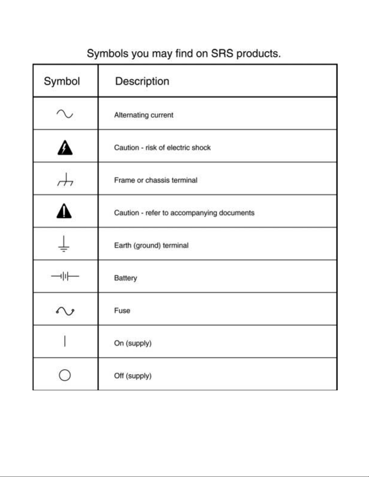
Symbols 2
Specifications 3
Front Panel Summary 5
Abridged Command List 6
Status Byte Definition 7
Configuration Switches 7
Guide to Operation
Front Panel 8
Signal Inputs 8
Signal Filters 8
Sensitivity 8
Dynamic Reserve 9
Status Indicators 9
Display Select 9
Output 9
Expand Function 9
Rel Function 9
Offset 10
Time Constants 10
Noise Measurements 10
Reference Input and Trigger Levels 11
Phase Controls 11
Power Switch 12
Local/Remote Operation 12
Default Settings 12
Rear Panel 13
AC Power 13
GPIB (IEEE-488) Connector 13
RS232 Interface 13
Signal Monitor Output 13
Pre-Amp Connector 13
A/D Inputs and D/A Outputs 13
Ratio Feature 13
Internal Oscillator 13
Guide to Programming
Communications 15
Command Syntax 15
Status LED's 15
RS232 Echo Feature 16
Try-out with an ASCII Terminal 16
Command List 17
Status Byte 20
Errors 20
Reset Command 20
Trouble-Shooting Interface Problems 21
Common Hardware Problems 21
Common Software Problems 21
RS232 Interface
Introduction to the RS232 21
Data Communications Equipment 22
Wait Command 22
Termination Sequence 22
GPIB (IEEE-488) Interface
Introduction to the GPIB 22
GPIB Capabilities 22
Response to Special GPIB commands 22
Serial Polls and SRQ's 23
Echo Mode using the RS232 23
Using Both the RS232 & GPIB 23
Lock-in Technique
Introduction to Lock-in Amplifiers 24
Measurement Example 24
Understanding the Specifications 25
Shielding and Ground Loops 25
Dynamic Reserve 26
Current Input 26
Auto-Tracking Bandpass Filter 26
Notch Filters 27
Frequency Range 27
Noise Measurements 27
Output Filters 27
Ratio Capability 27
Computer Interface 27
Internal Oscillator 27
SR510 Block Diagram
Block Diagram 28
Signal Channel 29
Reference Channel 29
Phase-Sensitive Detector 29
DC Amplifier and System Gain 29
Microprocessor System 29
Circuit Description
Introduction 30
Signal Amplifier 30
Current Amplifier 30
Notch Filters 30
Bandpass Filter 30
Reference Oscillator 31
PSD, LP Filters and DC Amplifier 31
Analog Output 31
A/D's 31
D/A's 32
Expand 32
Front Panel 32
Microprocessor Control 32
i
Page 4

RS232 Interface 32
GPIB Interface 32
Power Supplies 33
Internal Oscillator 33
Calibration and Repair
Introduction 34
Multiplier Adjustments 34
Amplifier and Filter Adjustments 34
CMRR Adjustment 34
Line Notch Filter Adjustment 35
2xLine Notch Filter Adjustment 35
Repairing Damaged Front-End 35
Appendix A: Noise Sources and Cures
Johnson Noise 36
'1/f' Noise 36
Noise Spectrum 36
Capacitive Coupling 37
Inductive Coupling 37
Ground Loops 38
Microphonics 38
Thermocouple Effect 38
Appendix B: RS232
Simplest Case Using the RS232 39
Using Control Lines 39
Baud Rates 39
Stop Bits 40
Parity 40
Voltage Levels 40
'Eavesdropping' 40
Appendix C: GPIB
Introduction to the GPIB 41
Bus Description 41
Appendix D: Program Examples
IBM PC, Microsoft Basic, via RS232 42
IBM PC, Microsoft Fortran, via RS232 43
IBM PC, Microsoft C, via RS232 45
IBM PC, Microsoft Basic, via GPIB 47
HP-85, HP Basic, via HPIB 49
Documentation
Part Numbering and Locations 50
Parts List, Main Assembly 51
Parts List, Internal Oscillator 65
Parts List, Miscellaneous 66
Parts List, Front Panel 67
Schematic Diagrams 71
ii
Page 5

Safety and Preparation for Use
***CAUTION***: This instr um ent m ay be damaged if oper at ed with the LINE VOLTAG E SELECTOR set f or
the wrong applied ac input-sour ce volt age or if the wrong f use is installed.
LINE VOLTAGE SELECTION
The SR510 operates fr om a 100V, 120V, 220V, or
240V nominal ac power source having a line
frequency of 50 or 60 Hz. Before connecting the
power cord to a power source, v erify that the LINE
VOLTAGE SELECTOR car d, located in the rear
panel fuse holder, is set so that the correct ac input
voltage value is visible.
Conversion to other ac input volt ages requires a
change in the fuse holder volt age car d pos ition and
fuse value. Disconnect the power cord, open the
fuse holder cover door and rotat e the fuse-pull lever
to rem ove the fuse. Remove the small printed circuit
board and select t he oper at ing voltage by orienting
the printed c ircuit boar d to position the desir ed
voltage to be visible when pushed firmly into it s slot .
Rotate the fuse-pull lever back into its normal
position and insert t he cor r ect fuse into the fuse
holder.
LINE FUS E
Verify that the correct line fuse is installed befor e
connecting the line cord. For 100V and 120V, use a
½ Amp fuse and for 220V and 240V, use a 1/4 Amp
fuse.
OPERATE WITH COVERS IN
PLACE
To avoid personal injury, do not remov e the
product cov er s or panels. Do not operate the
product without all covers and panels in place.
WARNING REGARDING USE
WITH PH OTOMULTIPLIERS
It is relatively easy to dam age t he signal inputs if
a photomultiplier is used improper ly with t he
lock-in amplifier. W hen left c ompletely
unt erminated, a PMT will charge a c ab le t o a
few hundred volts in a ver y short time. If this
cable is connected to t he lockin, the stored
charge may dam age the front-end transist or s.
To avoid this problem, pr ovide a leakage path of
about 100 KΩ to ground inside the base of the
PMT to prev ent charge acc um ulation.
LINE CORD
This instrument has a det achable, three- wire power
cord with a thr ee- contact plug for connect ion to both
the power sourc e and pr otective gr ound. The
protect ive gr ound cont ac t connect s to the accessible
metal part s of the instr um ent. To prevent electrical
shock, always use a power sour ce out let that has a
properly grounded pr ot ec t ive- gr ound cont act.
1
Page 6
2
Page 7

SR510 Specification Summary
General
Power 100, 120, 220, 240 VAC (50/60 Hz); 35 Watts Max
Mechanical 17" x 17" x 3.5" (Rack Mount Included) 12 lbs.
Warranty Two years parts and labor.
Signal Channel
Inputs Voltage: Single-ended or True Differential
Current: 10
Impedance Voltage: 100 MΩ + 25 pF, ac coupled
Current: 1 kΩ to virtual ground
Full Scale Voltage: 100 nV (10 nV on expand) to 500 mV
Sensitivity Current: 100 fA to 0.5 µA
Maximum Voltage: 100 VDC, 10 VAC damage threshold
Inputs 2 VAC peak-to-peak saturation
Current: 10 µA damage threshold
1 µA ac peak-to-peak saturation
Noise Voltage: 7 nV/√Hz at 1 kHz
Current: 0.13 pA/√Hz at 1 kHz
Common Mode Range: 1 Volt peak; Rejection: 100 dB dc to 1KHz
Above 1KHz the CMRR degrades by 6 dB/Octave
Gain Accuracy 1% (2 Hz to 100KHz)
Gain Stability 200 ppm/°C
Signal Filters 60 Hz notch, -50 dB (Q=10, adjustable from 45 to 65 Hz)
120 Hz notch, -50 dB (Q=10, adjustable from 100 to 130 Hz))
Tracking bandpass set to within 1% of ref freq (Q=5)
Dynamic Reserve 20 dB LOW (1 µV to 500 mV sensitivity)
40 dB NORM (100 nV to 50 mV sensitivity)
60 dB HIGH (100 nV to 5 mV sensitivity)
Bandpass filter adds 20 dB to dynamic reserve
Line Notch filters increase dynamic reserve to 100 dB
6
Volts/Amp
Reference Channel
Frequency 0.5 Hz to 100 kHz
Input Impedance 1 MΩ, ac coupled
Trigger SINE: 100 mV minimum, 1Vrms nominal
PULSE: ±1 Volt, 1 µsec minimum width
Mode Fundamental (f) or 2nd Harmonic (2f)
3
Page 8

Acquisition Time 25 Sec at 1 Hz
6 Sec at 10 Hz
2 Sec at 10 kHz
Slew Rate 1 decade per 10 S at 1 kHz
Phase Control 90° shifts
Fine shifts in 0.025° s t eps
Phase Noise 0.01° r m s at 1 kHz, 100 msec, 12 dB TC
Phase Drift 0.1°/°C
Phase Error Less than 1° above 10Hz
Demodulator
Stab ility 5 ppm /°C on LOW dynamic reserv e
50 ppm/°C on NORM dynamic reserve
500 ppm/°C on HIG H dynam ic reserve
Time Constants Pre: 1msec to 100 s ec (6 dB/Octav e)
Post: 1sec, 0. 1 sec, none (6 dB/Octave) or none
Offset Up to 1X full scale (10X on expand)
Harmonic Rej -55 dB (bandpass f ilter in)
Outputs & Interfaces
Outputs X (RcosØ), X Offset, Noise
Output Meter 2% Precision mirror ed analog m et er
Output LCD Four digit aut o- r anging LCD display shows same values as t he analog m et er s
Output BNC ±10 V output corresponds to full scale input
<1Ω output impedance
Reference LCD Four digit LCD display for r eference phase shift or frequency
RS232 Int er f ace contr ols all funct ions. Baud rates from 300 to 19.2 K
GPI B Inter face cont r o ls a ll f u n c tions. (I EEE-488 Std)
A/D 4 BNC inputs with 13 bit resolution ( ± 10. 24 V)
D/A 2 BNC outputs with 13 bit r esolution ( ± 10. 24 V)
Ratio Ratio output equals 10X output divided by the Denom inator input .
Interna l Oscillat o r Range: 1 Hz to 100 kHz, 1% accuracy
Stability: 150 ppm/°C
Distortion: 2% THD
Amplitude: 1% accurac y, 500 ppm/°C st ability
4
Page 9

Front Panel Summary
Signal Inputs Single Ended (A), Tr ue Diff erential (A-B), or Current (I)
Signal Filters Bandpass: Q-of- 5 Auto-tracking f ilter (In or Out)
Line Notch: Q- of - 10 Notch Filter at line frequency ( I n or Out)
2XLine Notch: Q-of - 10 Notch Filter at twice line frequency ( I n or Out)
Sensitivity Full scale sensitivity f r om 100 nV to 500 mV RMS for voltage inputs
or fr om 100 fA to 500 nA RMS for current inputs.
Dynamic Reserve Select Dynam ic Reserve Stability Sensitivity Rang es
LOW 20 dB 5 ppm 1 µV to 500 mV
NORM 40 dB 50 ppm 100 nV to 50 mV
HIGH 60 dB 500 ppm 100 nV t o 5 mV
Status I ndicat or s OVLD Signal O ver load
UNLK PLL is not locked to the referenc e input
ERR I llegal or Unrecognized command
ACT RS232 or GPIB interface Activity
REM Remot e m ode: front panel has been locked-out
Display Select X Signal Amplitude at t he select ed phase ( AcosØ )
OFST Display the off set which is being added to the signal output
NOISE Compute and display t he noise on t he signal
Analog Meters Displays Signal, Offset, or Noise as a fraction of full scale
Output LCD's Displays Signal, Offset, or Noise in absolute units
Output BNC's Output follows Analog Meter, ± 10 V for ± full scale
Expand Multiplies the Analog Met er and Out put voltage by a factor X1 or X10.
REL Set the Offset to null the output: subsequent readings are relat ive readings.
Offset Enables or Disables Offset, and allows any offset (up to full scale) to be enter ed.
Time Constants Pre-filter has time const ant s from 1 mS to 100 S (6 dB/Octave)
Post-f ilter has time const ant s of 0, 0.1 or 1.0 S (6 dB/Octave)
ENBW Equivalent Noise Bandwidth. Specifies t he bandwidth when making Noise
measurem ent s. (1Hz or 10 Hz ENBW)
Reference I nput 1 MΩ Input, 0. 5 Hz to 100 KHz, 100 mV minimum
Reference Tr igger Trigger on r ising edge, z er o cr os sing, or f alling edge
f/2f Mode PLL can lock t o eit her X1 or X2 of the reference input frequency
Phase Controls Adjust phase in smoothly accelerating 0.025° steps , or by
90° steps. Pres s both 90° buttons to zero the phase.
Reference LCD Display refer enc e phase sett ing or r eference frequenc y
Power Switch Instr um ent settings f r om the last use are recalled on power-up
5
Page 10

Abridged Command List
A Return t he ‘REL’ Status
A0 Turn t he ‘REL’ off
A1 Turn t he ‘REL’ on
B Return Bandpass Filter St at us
B0 Take out t he Bandpass Filter
B1 Put in the Bandpass Filter
C Retur n the Reference LCD Status
C0 Display the Reference Fr equency
C1 Display t he Ref er ence Phase Shift
N Retur n the ENBW sett ing
N0 Select 1 Hz ENBW
N1 Select 1 0 Hz ENBW
O Ret ur n O ffs et Stat us
O0 Turn off Offset
O1,v Turn on Offset, v = offset
P Return t he Phase Set t ing
Pv Set the Phase to v. Abs(v) < 999 deg
D Retur n Dynam ic Reserve Set t ing
D0 Set DR to LOW range
D1 Set DR to NORM range
D2 Set DR to HIGH range
En Return Expand St at us
En,0 Turn Expand off
En,1 Turn Expand on
F Return the Ref er ence Fr equenc y
G Ret ur n t he Sensit ivity Set t ing
G1 Select 10 nV Full-Scale
... (G 1- G3 with SRS preamp only)
G24 Select 500 mV Full-Scale
H Retur n Pr eam p St at us (1=inst alled)
I Ret ur n t he Rem ot e/ Local Status
I0 Select Local: Fr ont panel act ive
I1 Select Remote: Front panel inactive
I2 Sele c t Remote with f u ll lo c k -out
J Set RS232 End-of-Record to <cr>
Jn,m,o,p Set End-of-record to n,m,o,p
K1 Simulates Key-pr ess of button #1
... (see un- abr idged comm and list)
K32 Simulates Key- pr ess of but t on #32
Q Ret ur n t he value shown on t he Output
LCD
R Retur n the trigger mode
R0 Set the trigger for rising edge
R1 Set the trigger for + zero crossing
R2 Set the trigger for falling edge
S Return t he display st at us
S0 Disp lay X = Aco s Ø
S1 Display Offset setting
S2 Dis play Noise
T1 Return pre-filter setting
T1,1 Set the pre-filter TC to 1 mS
...
T1,11 Set the pre-filter TC to 100 S
T2 Return the post-filter sett ing
T2,0 Remove post filter
T2,1 Set the post filter TC to 0.1 S
T2,2 Set the post filter TC to 1.0 S
V Return t he value of the SRQ mask
Vn Set the SRQ Mask to the value n
(See the Stat us Byte def inition)
W Return the RS232 wait inter val
Wn Set RS232 wait interval to nX4mS
L1 Return Stat us of Line Notch Filter
L1,0 Remove Line Notch Filter
L1,1 Insert Line Notc h Filter
L2 Return Stat us of 2XLine Filter
L2,0 Remove 2XLine Notch Filter
L2,1 Insert 2XLine Notch Filter
M Return t he f/2f Stat us
M0 Set refer enc e mode to f
M1 Set refer enc e mode to 2f
Xn Return t he v oltage at the rear panel
analog port n. ( n from 1 to 6)
X5,v Set analog port 5 to voltage v
X6,v Set analog port 6 to voltage v
Y Return t he St at us Byte value
Yn Test bit n of the Status Byte
Z Reset to def ault s ettings and cancel
all pending command
6
Page 11

Status Byte Definition
Bit Meaning
0 Magnitude too small to calculat e
phase
1 Command Parameter is out-of -range
2 No detectable refer ence input
3 PLL is not locked to the reference
4 Signal Overload
5 Auto-off set failed: signal too large
6 SRQ generated
7 Unrecognized or illegal command
Configuration S witches
There are t wo banks of 8 switches, SW1 and
SW2, located on t he rear panel. SW1 sets the
GPIB address and SW2 set s the RS232
paramet er s. The conf igurat ion switches ar e read
continuously and any changes will b e e ffective
immediately.
SW1:GPIB Mode Switches
Bit Example Function
1 } up GPIB Address Switches
2 } up Address 0 to 30 allowed
3 } up 'up' for bit = 1
4 } down 'down' f or bit = 0
5 } up (Most Significant Bit)
6 down 'down' t o echo on RS232
(norm ally 'up')
7 up Not Used
8 up Not Used
If the GPIB mode switches ar e set as shown in the
example column above, t hen the lockin will be
addressed as G PIB device #23, and all GPI B
commands and dat a will b e e c hoed over t he
RS232 for de-bugging purposes.
SW2:RS232 Mode Swi t ches
Bit 1 Bit 2 Bit 3 Baud Rate
up up up 19200
down up up 9600
up down up 4800
down down up 2400
up up down 1200
down up down 600
up down down 300
Bit Setting Explanation
4 up Odd parity
down Even parit y
5 up No par ity
down Parit y enabled
6 up No echo ( f or comput er )
down Echo mode ( for terminal)
7 up Two st op bits
down O ne st op bit
8 unused
Eight data bits ar e always sent, regar dless of the
parity set t ing. The most significant bit is always
zero.
Example: Bit 1 'down' and all others 'up' for
RS232 communication at 9600 baud, no par it y,
two stop bits, and no echo or prom pt s by the
SR510.
7
Page 12

SR510 Guide to Operation
Front Panel
The front panel has been designed to be almost
self-explanator y . The effec t of each key press is
usually reflected in the c hange of a near by LED
indicator or by a change in t he quant it y shown on
a digital display. This discussion explains each
section of t he front panel, pr oceeding left to right .
Signal Inputs
There are t hr ee input connector s locat ed in the
SIGNAL INPUT section of the front panel. The
rocker switch locat ed abov e t he B input selects
the input mode, either single-ended, A, differential,
A-B, or current , I.
The A and B inputs are voltage inputs with 100
MΩ, 25 pF input impedance. Their connector
shields are isolated from t he c hassis gr ound by
10Ω. These inputs are pr otect ed to 100V dc but
the ac input should never ex ceed 10V peak. The
maximum ac input bef ore overload is 1V peak.
The I input is a current input with an input
impedance of 1 KΩ to a virtual ground. The
largest allowable dc curr ent before overload is 1
µA. No current larger than 10 mA should ever be
applied to t his input. The conver sion ratio is 10
V/A, thus , the full scale current sensit ivities r ange
from 100 fA to 500 nA with a max ac input before
overload of 1 µA peak. You should use short
cables when using the cur r ent input.
6
allowable signals at t he inputs . The notch
frequencies ar e set at the factory to either 50 Hz
or 60 Hz. The user can adjust these frequencies.
(See the Maint enance and Repair section for
alignment details.) These f ilter s pr ecede the
bandpass filter in t he signal amplifier.
The bandpass filter has a Q of 5 and a 6 dB roll off
in either direction. Thus, the pass band (between
70% pass points) is always equal to 1/5t h of the
center frequency . The center frequenc y is
continually adjusted t o be equal t o t he internal
demodulator f r equenc y. When the refer ence
mode is f, the filter tracks the reference. When the
mode is 2f, the filter frequency is t wice the
refer ence input frequency. The center frequency
tracks as fast as the reference oscillator c a n s lew
and may be used during frequency sc ans. The
bandpass filter adds up to 20 dB of dynamic
reserve f or noise signals outside the pass band,
and increases the har m onic r ejection by at least
13dB. (2nd harm onic attenuat ed by 13 dB, higher
harmonics at t enuat ed 6dB/ octave more.) If not
needed to improve the dynamic reserve or the
harmonic reject ion t hen t he filter should be left
OUT.
Sensitivity
The sensitivity is displayed as a v alue (1- 500) and
a scale (nV, µV, mV). When using the current
input, which has a gain of 106 V/A, these scales
read fA, pA, and nA. The two keys in the
SENSITIVITY section mov e t he sensit ivity up and
down. If eit he r key is held d o wn, the s en s itivity will
continue to change in the des ired direc t ion four
times a second.
Signal Filters
There are t hr ee user selectable signal filters
available; a line frequency not ch, a 2X line
frequency notch, and an auto-tracking bandpass.
Each of the filters has a pair of indicator LED's and
a function key locat ed in the SIG NAL FILTERS
section of t he front panel. Pres sing a key will
toggle the st at us of the appropr iate filter. The
status of each filter is displayed as IN, filter active,
or OUT, fi l te r in a c tive .
The notch filter s have a Q of 10 and a depth of at
least 50 dB. Thus, the line fr equency not c h is 6
Hz wide and the 2X line notch has a width of 12
Hz. Both of these filters can incr ease the dynamic
reserve up t o 50 dB at the notch frequencies. The
achievable reser ve is limited by the maximum
The full scale sensitivit y can r ange from 100 nV to
500 mV. The sensitivit y indication is not changed
by the EXPAND func t ion. The EXPAND function
increases the out put s ensit ivity ( Volts out / volts in)
as well as the resolution of t he digital output
display.
Not all dynamic reserves ar e av ailable at all
sensitivities. I f the sensitivity is changed to a
setting f or which the dynamic r eser ve is not
allo we d , the dy n a mic res e r v e will c hange t o the
next setting which is allo we d. Sensitivity takes
precedence over the dynamic reserve. The
sensitivity range of eac h dynam ic res er ve is
shown below.
8
Page 13

Dynamic Reserve Sensitivity Ran ge
LOW 1 µV through 500 mV
NORM 100 nV t hr ough 50 m V
HIGH 100 nV thr ough 5 m V
Dynam ic Reserve
REM indicates t hat t he unit is in the remote state
and that the front panel cont r ols ar e not operative.
There are t wo remote stat es. The Remot e-WithLock o ut will not a llow any inputs from the front
panel. The Remote- Wit hout - Lock out comm and
allows you to return the front panel to operation by
pressing the DI SPL AY UP key.
The dynamic reser ve ( DR) is set using the keys in
the DYNAMIC RES ERVE section. The r eser v e is
displayed by the three indicator LED's, HIGH,
NORM, LOW. Only those dynamic reserve
settings available for the sensitivity are allowed
(see above table) . For example, when the
sensitivity is 500 mV, the DR will always b e LOW.
The dynamic reser ve and out put st ability of e a c h
setting ar e shown below.
Setting Dy n amic Reserve Ou tput Sta bility
(ppm/°C)
LOW 20 dB 5
NORM 40 dB 50
HIGH 60 dB 500
Since a higher DR results in degraded output
sta b ility, y ou s hould use t he lowest DR sett ing f or
which there is no overload indication. Note t hat
using the Bandpass Filter prov ides about 20dB of
additional DR and so allows you to oper at e with a
lower DR s etting .
Status
Dip lay Sel ect
The keys in the DISPLAY section select the
paramet er to be displayed on the out put meters
and the output on the OUT PUT BNC connector.
The displayed param et er is indicated by one of t he
three LED’s and can be either t he demodulator
output ( X), the offset (OFST), or the rm s noise
(NOISE). When displaying NOISE, the equivalent
noise bandwidth (ENBW) is se lec ted in t h e TIME
CONSTANT section.
Output
The analog output is available at t he OUTPUT
BNC. The input signal equal t o t he s elected full
scale sensitivity will generate a ± 10V out put when
the EXPAND function is off. With the EXPAND on,
the output is multiplied by 10, eff ectively
increasing the full scale sensitivity by 10. The
ouptut impedanc e is <1Ω and t he output current is
limited to 20 mA.
The analog meter always displays the OUTPUT
voltage. Accur acy is 2% of full scale.
There are f ive STATUS LED's.
OVLD indicates a signa l over load. This condition
can occur when the signal is too large, the
sensitivity is too high, the dynamic reserve is too
low, the off set is on, the expand is on, the time
constant is not lar ge enough, or the ENBW is too
large.
UNLK in d ic ates t h at the referen c e o s c illator is n o t
phase locked to the external refer enc e input. This
can occur if the ref erence amplitude is t oo low, t he
frequency is out of range, or the trigger m ode is
incorrect f or the refer ence s ignal waveform .
ERR flashes when an er r or occ ur s on one of the
computer int erfaces, such as an incorrect
command, invalid parameter, etc.
ACT indicates act ivity on t he com put er interfaces.
This LED blinks every tim e a char act er is received
by the SR510 or transmit t ed by the SR510.
The OUTPUT LC D disp lay pr ovides a r ead- out of
the displayed paramet er in r eal units. The scale of
the displayed quantity is indicated by t he t hr ee
scale LED's to the r ight of the display. This readout auto r anges and will re flect the sens itivity
added when the EXPAND f unc t ion is on.
Expand
The output EXPAND is toggled by pressing the
key in the EXPAND section. The expand status is
indicated by the X10, ex pand on, and the X1,
expand off, LED's.
REL Function
The relative (aut o- zer o) func t ion is toggled by the
key in the REL section. Every time t he rel stat us
LED is turned ON the offset value is set to minus
the value of t he X output, thus zeroing the X
out p ut. This function will work e v en if X is not the
9
Page 14

current ly displayed param et er . If the output is
greater than 1.024 t im es full scale, the REL
fun c tion will not b e a ble to zer o the output and the
ON LED will blink . The of fset v a lue will then be set
to its max value. If NOISE is being displayed when
the REL function is turned on, the noise ouptut will
require a sew seconds to s ettle again.
If the manual OFFSET in ON when the REL
function is tur ned on, t he manual OFFSET will be
turned OFF before the auto zero is done.
The REL func t ion and t he m anual OFFSET are
both ways to ent er the offs et value. When the REL
function is tur ned off using t he REL key the offset
is turned of f but the value is not lost. If the manual
OFFSET is now tur ned ON, the off s et will b e that
set by the REL funct ion.
Offset
The OFFSET section controls the manual
OFFSET. The offset is turned ON and OFF using
the upper key in the OFFSET section. When the
offset is ON, the lower two keys are used to set
the amount of offset. A single key press will
advance the of f set by 0.025% of full scale. If the
key is held down, the off set advances in larger and
larger increments, the largest increment being
10% of full scale. When the offs et is turned OFF
the applied offset r eturns to zero but the offset
value is not lost. The next pres s of the upper
offset key (ret ur ns to ON) sets the offset to the
previously entered value.
If an attempt is made to advance the offset v alue
beyond full scale, the OFFSET ON LED will blin k .
An offset up to 1.024 tim es the full scale sensitivity
may be enter ed. When the expand is on, this is
10X the full scale output.
If the REL function is ON when the manual
OFFSET is t ur ned ON, the REL funct ion is tur ned
OFF but the off set value rem ains the same. The
OFFSET key s m ay now be used t o adjust this
offset value.
Note that the offsets (either manual off set or those
generated by t he REL function) represent a
fract ion of the full scale reading, and so their
absolute value will change when the s ensitivity
scale is changed. A signal which has been nulled
by an offset will n o t be nulled when t he sens itivity
scale is changed. The analog meter and the
output BNC indicate the sam e value given by the
equation:
V
= 10Ae(AvVicosØ+Vos)
out
where...
Ae= 1 or 10 per the Expand setting
Av= 1/Sensitivity
Vi= m agnitude of the signal
Ø = phase between signal & reference
Vos= of f s et (fract ion of FS < 1.024)
Time Constant
There are t wo post demodulator low pass f ilters ,
labeled PRE and POST. The PRE filter precedes
the POST filter in the output amplifier. Each filter
provides 6 dB/oct attenuat ion.
The PRE filter t im e const ant ranges from 1 mS to
100 S and is selected by the two keys below the
PRE filter indicator LED's. Holding down either
key will a d v ance the time constant twic e a s ec o n d
in the desired direction.
The POST filter time constant can be set to 1 S or
0.1 S, or can be removed altogether, NONE, using
the two keys below the ENBW indicators. When
set to NONE, the total attenuat ion is that of the
PRE filter, or 6 dB/ oct. When the POST filter is 1
S or 0.1S, the total attenuation is 12 dB/oct for
frequency c om ponent s beyond the larger of the
POST and PRE f ilter bandwidths ( r ecipr ocal tim e
constant).
Noise
When the DISPLAY is set to NOISE, none of the
PRE and POST ind icat or LED's ar e on. Inst ead,
one of the two ENBW indicator s will be on,
showing the Equivalent Noise Bandwidth of the
rms noise calculation. The ENBW is set using the
keys below the ENBW indicator LED's (same keys
as used to set the POST f ilter ). The PRE filter
keys do nothing in this case. Pressing the upper
key when the bandwidth is already 1 Hz will reset
the rm s noise average (out put) to zero, res t arting
the calculation. Likewise with pr ess ing the lower
key when 10 Hz is already selected.
The noise is the rms dev iation of the out put within
a 1 or 10 Hz equivalent noise bandwidth about the
refer ence frequency . A dc output does not
contribut e t o the noise, the noise is determ ined
10
Page 15

only by the ac 'wiggles' at t he output. By
measuring the noise at dif f erent frequencies, t he
frequency dependenc e of t he noise densit y can be
found. This usually has the form of v
The noise computat ion assum es t hat t he noise
has a Gaussian distr ibution ( such as J ohnson
noise). Since the com put ation takes m any time
constant s (reciproc al bandwidt h) , t he noise output
should be allowed to approach a st eady value
before a r eading is taken. For the 1 Hz ENBW,
this time is on the order of 15 to 30 seconds; for
the 10 Hz ENBW , the o utp ut stabilizes much
fas ter. The n ois e o u tput will var y s lig htly sinc e
the re will alwa y s b e n o is e v a riation s that a r e s lo w
compared t o the bandwidth. Any DC component
in th e ou tput will n o t cont ribute to the noise.
Howeve r , a larg e DC ou tput will c a u s e the nois e
computat ion t o initially rise to a large value bef or e
approaching the f inal answer. As a r esult, t he
com p utatio n will take longer to settle.
To obtain a value for the noise density, t he noise
reading should be divided by the squar e r oot of
the ENBW. Thus, when the ENBW is 1 Hz, the
noise output is the noise densit y, and when t he
ENBW is 10 Hz, the noise density is the noise
output divided by √10. For exam ple, if the input
noise is measured to be 7 nV with the ENBW set
to 1 Hz, the noise density is 7 nV/√Hz . Swit c h in g
the ENBW to 10 Hz results in a faster
measurem ent and a reading of 22 nV on the
output. The noise density is 22 nV/√10 Hz or 7
nV/√Hz. At frequencies » 10 Hz, the noise
density should be independent of t he ENBW.
noise ~
1/f.
Reference and Trigger Level
The REFERENCE I NPUT BNC is lo c a ted in t his
section. The input is ac c oupled and the
impedance is 1 MΩ. The dc voltage at this input
should not exceed 100 V and the largest ac signal
should be less than 10 V peak. The t hree
indicators above the input BNC display t he
TRIGGER MODE. The single key above the input
BNC is used to select the TRIGGER MODE.
If the center TRIGGER MODE LED is on, the
mode is SYMMETRIC and the reference oscillator
will lock to the positive zer o cr oss ings of the ac
refer ence input . The ac signal must be symmetric
(e.g. sine wave, s quar e wave, etc.) and have a
peak to peak amplitude gr eat er t han 100 mV. A
signal with 1 Vrms am plitude is r ecommended.
The phase accuracy of the reference channel is
specified for a 1Vr m s sinewave in the symmetric
trigger m ode.
If the upper TRIGGER MODE LED is on, the
mode is POSITIVE. The trigger threshold is +1V
and the ref erence oscillator will lock t o the positive
going transitions of t he refer ence input . This
mode tr iggers on the rising edges of a TTL type
pulse train. The pulse width mus t be great er than
1 µS.
If the lo w e r TRIGGER MODE LED is on, the mode
is NEGATIVE. The trigger threshold is -1V and
the referen c e o s c illa tor wil l lo c k to the negative
going transitions of t he refer ence input . This
mode tr iggers on a negative pulse tr ain or on the
falling edges of a TTL type pulse t r ain
(rem em ber ing that t he input is ac coupled). The
pulse width must be greater than 1 µS.
Above the TRIGGER MODE indicators are the
REFERENCE MO DE LED's. The key below the
REFERENCE MO DE indicators toggles bet ween f
and 2f. When the MODE is f, the lock-in will
detect s ignals at t he refer ence input fr equency.
When the MODE is 2f, the lock-in det ect s signals
at twice the refer ence input frequency . In either
case , the referen c e os c illa tor ha s a ma x im u m
frequency of 100 KHz, thus, when in the 2f mode,
the ref erence input f r equency may not exceed 50
KHz.
The REFERENCE DIGITAL DISPLAY shows
eith e r the ref erence o s c illa tor f r equenc y or
phaseshift. The displayed parameter toggles
between the t wo whenever t he SELECT key is
pressed. The appr opr iat e sc ale indicator below
the display will be on. It is useful to check the
frequency display t o ver if y that the lock-in has
correct ly locked t o y our ref erence. The reference
frequency is m easur ed to 1 part in 256 resolution.
Phase Controls
The phase shift bet ween t he refer ence osc illator
and the ref erence input is set using the f our keys
in the PHASE section. The t wo keys below the
FINE label increment t he phase setting in small
amounts. A single key press will change t he
phase by 0.025 degrees in the desir ed direction.
Holding the key down will continue to change the
phase with larger and larger s t eps with t he largest
step being 10 degrees. The two 90° keys are
used to change t he phase by 90 degree
increments . The upper key will add 90 degrees
and the lower key will su btract 90 degrees.
Holding both keys down at once s et s the phase
shift back to zero. The REFERENCE DIGITAL
DISPLAY automatically displays t he phas e
11
Page 16

whenever any of t he PHASE key s ar e pr essed.
The phase ranges fr om -180 degr ees to +180
degrees and is the phase delay f r om the refer ence
input signal.
Power
This is the instrume n t's POWER switch. When the
power is turned of f, the front panel settings are
retained so t hat the inst r ument will retur n to the
same settings when the power is next turned on.
When the power is tur ned on, the OUTPUT
DIGITAL DISPLAY will show the SERIAL
NUMBER of the instr ument and REFERENCE
DISPLAY shows the model number of the
instrument. All displays return to normal after 2
seconds.
Local and Remote
When the instr um ent is progr ammed via the
computer int erface t o be in the REMOTE state
WITHO UT LO CK-OUT, the DISPLAY UP key will
return the instrument to LOCAL f ront panel
control. If the instr ument is in the REMOTE WITH
LOCK-OUT state, no front panel key will ret u r n the
status to LOCAL. In this case, a RETURN TO
LOCAL c om m and m ust be s ent over the computer
interfac e or the power must be turned off and back
on.
Defaults
If the REL key is held down when the POWER is
turned on, the instr um ent settings will be s et to the
defaults shown below instead of t he settings in
effect when the power was t ur ned off.
Parameter Setting
BANDPASS OUT
LINE OUT
LINE X 2 OUT
SENSITIVITY 500 mV
DYN RES LOW
DISPLAY X
EXPAND OFF
REL OFF
OFFSET OFF (value=0)
PRE TIME CONSTANT 100 mS
POST TIME CONST ANT 0.1 S
ENBW 1 Hz
REFERENCE MO DE f
TRIGGER MODE SYMMETRIC
REFERENCE DISPLAY FREQUENC Y
PHASE 0°
Whenever def ault values ar e used at power up,
the red ERR LED will turn on f or about 3 seconds.
If the ERR LED is on when the instrument is
powered on without the LOCAL key down, then
the instr um ent is ignoring the ret ained settings.
This can be due to a low battery.
12
Page 17

SR510 Guide to Operation
Pin Voltage Current Available
Rear Panel
AC Power
The ac line voltage selector car d, line fuse, and
line cord receptacle ar e located in t he f use holder
at the left side of the rear panel. See the section,
Preparati on f or Use at the front of this manual for
instruct ions on set t ing t he ac voltage selector and
choosing the corr ect fuse.
GPIB Connector
The SR530 has an IEEE 488 ( G PI B) int er f ace built
in. The GPIB addr ess is set using SW1 located to
the right of t he interface c onnect or s. Refer to
page 7 for switch sett ing details.
RS232 Connector
The SR530 has an RS232 interf ace. The
connector is conf igur ed as a DCE. The baud rate,
parity, st op bits, and echo mode are select ed
using SW2 locat ed t o t he r ight of the interface
connectors . Refer to Page 7 for switch setting
details.
Signal Monitor O utput
1 + 20 100 mA
2 + 5 10 m A
6 - 20 100 mA
7 Signa l gr ound
8 Digital ground
Gene ral Purpose A/D and D/A
There are f our analog input port s, labeled X1
through X4. These inputs may be digitized and
read via the com put er interfaces. The range is -
10.24 V to +10.24 V and the resolution is 2.5 m V.
The input impedance is 1 MΩ. A digitization can
be perfor m ed in about 3 mS but the result may
take longer t o transm it over the interf ac e being
used.
There are t wo analog output ports, labeled X5 and
X6. The voltages at t hese ports m ay be
program m ed via t he computer interfaces. The
range is -10.24 V to +10. 24 V and the resolution is
2.5 mV. The output impedance is <1Ω and the
output cur r ent is limited to 20 mA.
Ratio
Output X5 is the ratio output when not
program m ed by the computer interface or s et via
the fr ont panel. X5 becom es the ratio output
whenever the unit is t ur ned on.
This BNC provides the buf f er ed output of t he
signal amplifiers and f ilter s . This is the signal just
before t he dem odulat or. The output impedanc e is
<1Ω. When a full scale input is applied, the peakto-peak am plitude at this output is 20 mV, 200 mV
or 2 V for dynamic reserve settings of high, norm,
and low, respectively.
Preamp Connector
This 9 pin "D" connector provides power and
control signals to ext er nal per ipherals such as pr eamplifiers. The av ailable power is descr ibed
below.
The voltage at X5 is t he ratio of the det ected
signal output, X, t o the analog voltage at port X1.
An output of 10 V corres ponds to a ratio of 1. The
ratio is comput ed by digitizing the dem odulat or
output and t he voltage at port X1 and then taking
the rat io. The resolution is 0. 0025 V. For best
accuracy, t he sens itivity should be set to provide
at least a 50% full scale signal and the analog
denominator ( X1) should be 5V or greater. The
ratio is updated appr oxim at ely ever y 1. 5 mS. For
the Ratio feat ur e to work, the voltage at the
denominator input m ust ex ceed 40 mV.
Internal Oscillator
The INTERNAL OSCILLATOR is a voltage
controlled oscillat or with a sine wave output . To
use the osc illator as the ref erence s o urce, connect
the REF O UTPUT on the r ear panel to the REF
INPUT on the fr ont panel. The REF OUTPUT is a
1 Vrms sine wave. The SINE OUTPUT may be
used as the st imulus to the experiment . The SINE
13
Page 18

OUTPUT can be set to three amplitudes, 1 V, 100
mV, and 10 mV (rms) using t he amplitude switch.
The output impedanc e is 600Ω. The AMP CAL
screw adjusts t he am plitude.
The oscillator frequency is controlled by the VCO
INPUT voltage. A voltage f r om 0V to 10V will
adjust the f r equency ac cor ding t o the VCO
RANGE select ed. Thr ee r anges ar e available, 1
Hz/V, 100 Hz/V, and 10 KHz/V. The input
impedance is 10 kΩ. Th e FREQUENC Y CAL
screw adjusts t he frequency.
There are f our ways to set the frequency:
1) Connect X5 or X6 (D/A outputs) to the VCO
INPUT. The fr equency is now cont r ollable via the
computer int erfaces by pr ogr amming X5 or X6.
2) If the VCO INPUT is left open, then the
oscillato r will run at the top of its range (i.e. 10 Hz,
1 KHz, or 100 KHz).
3) A 10 KΩ potentiomet er may be connected from
the VCO INPUT to ground. This pot will then set
the fr equency .
4) Connect t he VCO INPUT to an exter nal voltage
source which can provide 0 to 10V.
In all four cases, if the REF OUTPUT is connected
to the REFERENCE I NPUT on the front panel, the
frequency m ay be read on the front panel
REFERENCE DIGITAL DISPLAY or via the
computer int erfaces.
14
Page 19

SR510 Guide to
Programming
An example of a multiple comm and is:
G 5; T 1,4; P 45.10 <cr>
The SR510 Lock-in Amplifier is r em ot ely
program m able via both RS232 and GPI B
interfac es. It may be used with laboratory
computer s or simply with a terminal. All front
panel features ( except signal input selection and
power) may be controlled and read via t he
computer int erfaces. The SR510 can also read
the analog output s of other laboratory instr um ents
using its four gener al pur pose analog input por t s.
There are also two pr ogr ammable analog output
ports available to prov ide general purpos e cont r ol
voltages.
Comm unicating with the SR510
Before using either the RS232 or GPIB interface,
the appropr iate c onf iguration switches need t o be
set. There are two banks of 8 switches, SW1 and
SW2, locat ed on t he rear panel. SW1 sets the
GPIB address and SW2 sets the RS232
paramet er s. The conf igurat ion switches ar e read
continuously and any changes w ill be e ffective
immediately. For details on switch settings, s ee
page 7 at the front of this manual.
Command Syntax
Communications with the SR510 use AS CII
character s . Commands to t he SR510 may be in
eith er UPPER or lower cas e .
It is not necessary to wait between comm ands .
The SR510 has a command input buf f er of 256
character s and pr ocess es the commands in the
order r eceived. Likewise, t he SR510 has an
output buf fer (for each interfac e) of 256
characters.
In general, if a command is sent without
paramet er s, it is inter pr eted as a request to read
the status of the associated f unction or setting.
Values returned by t he SR510 are s ent as a string
of ASCII char act ers t erminated usually by car r iage
retur n, line-feed. For example, after the above
command is sent , the following read commands
would generate the r esponses s hown below.
Command Response from t he SR510
G <cr> 5<cr><lf>
T 1 <cr> 4<cr><lf>
P <cr> 45.10< cr > < lf>
The choice of ter m inat ing characters sent by the
SR510 is determined by which interfac e is being
used and whether t he 'ec ho' feat ur e is in use. The
term inating sequence f or the GPIB interf ace is
always <cr>< lf > (with EOI). The default sequenc e
for RS232 is <cr> when the echo mode is off, and
<cr> < lf> when the echo mode is on. The
term inating sequence f or the RS232 interface may
be changed using the J comm and.
A command t o the SR510 consists of one or two
command letters, arguments or parameters if
necessary, and an ASCII carriage ret ur n (<cr>) or
line-feed (<lf > ) or both. The different part s of the
command do not need to be separated by spaces .
If spac es are included, they will b e ignor ed. I f
more t han one paramet er is required by a
command, the param et ers m ust be separated by a
comma. Examples of commands ar e:
G 5 <cr> set the sensitivity to 200 nV
T 1,4 <cr> set the pre filter to 30 mS
F <cr> read the reference frequency
P 45.10 <cr > set phase shift to 45. 10°
X 5,-1. 23E-1 < cr> set por t X5 to -0.123 V
Multiple commands m ay be sent on a single line.
The commands m ust be separ at ed by a semicolon
(;) character. The commands will n o t be exec u ted
until the ter m inating car r iage return is sent.
Note that the terminating char act er s are sent with
each value retur ned by t he SR510. Thus, the
response to the command string G;T1; P< cr > while
using the RS232 non-echo mode would be
5<cr>4<cr>45.10<cr>.
Front Panel S ta tus LED's
The ACT LE D f lashes whenever t he SR510 is
sending or receiving charact er s ov er the comput er
interfaces.
The ERR LED f lashes whenever an er r or has
occurred, s uch as, an illegal command has been
received, a par am et er is out of range, or a
communicat ion buff er has exceeded 240
character s . This LED flashes for about thr ee
seconds on power-up if t he batt er y voltage is
insufficient t o r et ain pr evious instr um ent settings.
15
Page 20

The REM LED is on whenever t he SR510 is
program m ed to be in the remote state.
RS232 Echo and No Echo
Operation
In order to allow the SR510 to be operat ed from a
term inal, an echo f eature has been included which
causes the unit t o echo back commands rec eived
over the RS232 port . This feature is enabled by
setting switch 6 on SW2 to the DOWN position. In
this mode, the SR510 will send line-feeds in
addition to carr iage returns with each value
retur ned and will a ls o s end the prompts 'OK>' and
'?>' t o indicate that the pr evious com m and line
was either processed or contained an error.
Operat ing t he SR510 fr om a terminal is an ideal
way to learn the commands and r es ponses bef ore
attem pt ing t o program a computer to contr ol the
SR510. When the unit is controlled by a
computer , the ec ho featur e should be turned off t o
prevent t he s ending of spurious characters which
the comput er is not expecting.
Try-Out with an ASCII Terminal
Before at t em pting any detailed program m ing with
the SR510, it is best to try out the commands
using a terminal. Connect a term inal with an
RS232 port to t he RS232 connector on t he rear
panel of the SR510. Set the baud rat e, parit y, and
stop bits t o match the term inal by setting SW2 per
the switch set t ing t able given on page 7. The
echo mode should be enabled (switch 6 DOWN).
After setting SW2 and connecting the term inal,
hold down the REL key whi le turning the unit on.
This causes the SR510 to assum e its def ault
settings so t hat t he following discussion will agree
with the actual re sponses of t he SR510. The ACT
and ERR LED's on t he front panel will f la s h for a
second and the sign-on m essage will appear on
the terminal. Following the m es sage, the prom pt
'O K> ' will be displa y e d. This indicat e s that th e
SR510 is ready to accept commands .
to the terminal.
Now read the gain using the sensitivity r ead
command, G<cr>. The response should be 24
meaning that the sensitivity is at the 24th setting or
500 mV. Change the sensit ivity by typing
G19<cr >. The sensitivity should now be 10 mV.
Check the fr ont panel to mak e sure this is so.
The output of the lock- in is read by typing the
command, Q1<c r >. The response is a signed
floating point number with up t o 5 significant digits
plus a signed exponent. Change the gain to 10 uV
using the G10 com m and. The response to the Q1
command will now be sim ilar to the pre v iou s o n e
except t hat the exponent is differ ent.
Attach a DC voltmeter to the X6 output on the rear
panel. The range should allow for 10V readings.
The voltage at t he X6 output can be set using the
X6 command. Type X6,5.0<cr> and the X6 output
will change to 5.0V. To read this back to the
terminal, just type X6<cr>. When setting the X6
voltage, t he volt age m ay be sent as an integer (5),
real (5.000) , or floating point ( 0. 500E1) num ber.
Now connect the X6 out put to the X1 input (also
on the rear panel). X1 through X4 ar e analog
input ports . To read the voltage on X1, si mply
type X1<cr>. The response 5.000 should appear
on the terminal. The analog port s X1 through X6
can be used by your computer to read outputs of
other inst r um ent s as well as to control other
laboratory par am eters.
At this point, the user should experiment with a
few of the comm ands. A detailed command list
follows.
Type the lett er 'P' followed by a carriage ret ur n
(P<cr> ). The SR510 responds by sending to t he
term inal the char acters 0.00 indicating that t he
phase is set to 0 degrees. In general, a command
with no argument s or param et ers reads a sett ing
of the unit. To set the phase to 45 degrees, type
the comm and, P45<cr >. To see that the phase
did change, use the SELECT k ey on t he front
panel to display the phase on the REFERENCE
DIGITAL DISPLAY. Typing the phase read
command, P< cr>, will now return the s tr in g 45 .00
16
Page 21

SR510 Command List
The first letter in each command sequenc e is the
command. The rest of the sequence consists of
paramet er s. Multiple parameter s ar e separated by
a comma. Those param eters shown in {} are
optional while those without { } ar e required.
Variables m and n represent integer parameters
while v represent s a real number. Parameter s m
and n must be expressed in integer f ormat while v
may be in integer, real, or floating point f ormat .
F
The F command r eads the refer ence frequency.
For example, if the ref erence frequency is 100 Hz,
the F comm and retur ns the string "100. 0". If the
refer ence frequency is 100. 0 kHz, the string
"100.0E+3" is ret ur ned. The F command is a read
only command.
G {n}
If n is included, the G command sets t he gain
(sensitivity) . If n is absent, the gain setting is
returned.
A {n}
If n is "1", the A command causes the auto offset
routine to r un. Every time an "A 1" command is
received, t he aut o offs et function is executed. If n
is "0", then the auto offset is tur ned off. If n is
absent, then the auto offset st atus is returned.
Note that if the manual offset is on, an "A 1"
command will turn o ff the m anual offset befor e
executing the aut o offs et funct ion.
B {n}
If n is "1", the B command sets the bandpass filter
in. If n is "0", the bandpass filter is taken out. If n
is absent, t hen the bandpass f ilter status is
returned.
C {n}
If n is "1", the C command sets the reference LCD
display to show the phase setting. If n is "0", the
LCD will display the refer enc e frequency. If n is
absent, the paramet er being displayed (frequency
or phase) is returned. Note that the P and F
commands ar e used to read the act ual values of
the phase and fr equenc y.
D {n}
If n is included, the D command s ets the dynamic
reserve. If n is absent, the dynamic reserve
setting is ret ur ned.
n Sensitivity
1 10 nV
2 20 nV
3 50 nV
4 100 nV
5 200 nV
6 500 nV
71 µV
82 µV
95 µV
10 10 µV
11 20 µV
12 50 µV
13 100 µV
14 200 µV
15 500 µV
16 1 mV
17 2 mV
18 5 mV
19 10 mV
20 20 mV
21 50 mV
22 100 mV
23 200 mV
24 500 mV
Note that sensit ivity sett ings below 100 nV are
allowed only when a pre-amplifier is connect ed.
n Dyn Res
0LOW
1NORM
2 HIGH
Note that not all dynamic reserv e settings ar e
allowed at every s ensit ivity.
E {n}
If n is "1", the E command turns the output expand
on. If n is "0", the expand is turned off. If n is
absent, the expand status is returned.
H
The H command reads t he pre-ampli f i er stat us.
If a pre-am plifier is connect ed, a "1" is returned,
otherwise, a "0" is r et urned. The H command is a
read only command.
I {n}
If n is included, the I command sets t he remotelocal st atus. If n is absent, the remote-local stat us
is returned.
17
Page 22

n Status
0 Local: all front panel keys ar e oper ative
1 Remote: front panel keys ar e not
operative. The display up key re t urns the
status to local.
20 Quad Down
21 Select Display (f/ phase)
22 Sensitivity Up
23 Sensitivity Down
24 Dyn Res Up
25 Dyn Res Do wn
26 Display Up
27 Display Down
2 Lock-out: front panel keys are not
operative. No key retur ns the status to
local. Another I command is needed t o
return to loc a l.
When using the GPI B interface, the REN, LLO,
and GTL comm ands ar e not implement ed. The I
command is used by bot h interf aces to set the
remot e- local status.
J {n1,n2, n3, n4}
The J command sets the RS232 end-of-record
character s sent by the SR510 to those specif ied
by the ASCII codes n1- n4. If no argument is
included, t he end- of-r ec or d sequence r eturns to
the default ( a carriage return) , other wise, up to
four char acters may be specified. The end- ofrecord r equired by the SR510 when receiving
commands is not affected.
K n
The K command simulat es a front panel key
press. The effect is exactly the same as press ing
the selected key onc e. The paramet er n is
required.
nKey
1 Post Time Constant Up
2 Post Time Constant Down
3 Pre Time Constant Up
4 Pre Time Constant Down
5 Offset Up
6 Offset Down
7 Zero Phase (Simultaneous 90¡ Up and
Down)
8 Line Notch Filter
9 Bandpass Filter
10 Line X 2 Notch Filter
11 Relative (Auto Offset)
12 Offset (On/Off)
13 Expand
14 Local (Display Up when REMOTE)
15 Reference Trigger M ode
16 Reference Mode (f/2f)
17 Degrees Up
18 Degrees Down
19 Quad Up
L m {,n}
The L command set s and reads the status of the
line notch filters. If m is "1", then the 1X line
notch is selected, if m is "2", the 2X line notch is
selected. The par am et er m is required. If n is "1",
the L command sets the selected f ilter in. If n is
"0", the select ed filter is t aken out. If n is absent,
the status of the selected filter is ret urned.
M {n}
If n is "1", the M command sets the reference
mode to 2f. If n is "0", the reference mode is set
to f. If n is absent, the reference mode is returned.
N {m}
If m is "1", the N command sets the ENBW to 10
Hz. If m is "0", the ENBW is set to 1 Hz. If m is
absent, the ENBW setting is retur ned.
O {n} {,v}
If n is "1", the O command turns the offset on. If n
is "0", the offset is tur ned off. If n is absent, the
offset st at us (on or off) is returned. (The value of
the off s et is read using the S and Q commands.)
If n is included, then v may also be sent. v is the
offset value up to plus or minus full scale in units
of volts. For example, to offset half of full scale on
the 100 µV sensitivity, v should be "50. 0E-6" or an
equivalent value. However, if the sensitivit y is
then changed to 200 µV, the off s et is now half of
the new full scale or 100 µV. When the sensitivity
is changed, the offset is retained as a const ant
fract ion of full scale rat her than as a voltage
refer r ed to the input. The expand funct ion will, o n
the other hand, preser v e the value of the offset as
an input refer r ed voltage. Once a value of v is
sent, the of f set may be turned off and on without
losing the offset value by using the O command
without the v par am eter. Note that if the auto
offset is on, an "O 1" command will t u rn the au to
offset of f and tur n the manual offset on without
changing the actual offset value.
P {v}
If v is absent, the P command returns the phase
setting f r om -180 to +180 degrees. When v is
included, t he phase is set to the value of v up to
±999 degrees.
18
Page 23

Q
The Q comm and retur ns the output reading in
units of volts . For an input signal of 50 µV on a full
scale sensitivity of 100 µV, the Q com m a n d will
retur n the string "50.00E-6". The parameter read
is the same as that being shown on the output
display and can be changed with the S command.
R {n}
If n is included, the R command s ets the reference
input t ri gger m ode. If n is absent, the trigger
mode is retur ned.
n Mode
0 Positive
1 Symmetric
2 Negative
S {n}
If n is included, the S comm and select s the
paramet er shown on the analog meter and output
digital display as well as the out put BNC. If n is
absent, the paramet er being displayed is returned.
n Display
0X
1 Offset
2Noise
T m {,n}
The T command sets and reads the stat us of the
tim e const a nt s. If m is "1", the pre time constant
is selected, if m is "2", the post time constant is
selected. The par am et er m is required. If n is
included, t he T c ommand set s the select ed time
constant . If n is absent, the setting of the selected
time const ant is retur ned.
n Pre Time Constant ( m=1)
11mS
23mS
310mS
430mS
5 100mS
6 300mS
71S
83S
910S
10 30 S
11 100S
n Post Time Constant ( m=2)
0 none
1 0.1 S
21 S
U m {,n}
The U command set s and reads the unit's ROM
calibration bytes. m is the address offset of the
byte, 0- 255. If n is absent, the value of the
addressed calibration byt e is r et ur ned. If n is
included, t he addr ess ed calibrat ion byt e is set to
the value of n, 0-255. The new value will be in
effect unt il the power is t urned off or a reset
command is issued. Use of this command is not
recommended.
V {n}
If n is included, the V comm and sets the GPIB
SRQ (s er vice r equest ) mask to t he value n. If n is
absent, the value of the SRQ mask is returned.
W {n}
The W command s et s and reads the RS232
character wait interval. If n is included, the SR510
will wait n*4 mS between charact er s sent over the
RS232 interface. This allows slow comput er
interfac es t o keep up. n can range from 0 to 255.
If n is absent, the wait value is ret urned. The wait
interval is set t o 6 on power-up.
X n {, v}
n designates one of t he 6 general purpose analog
ports locat ed on t he rear panel. If n is 1,2,3, or 4,
the X comm and will r e turn the v o ltage on the
designated analog input por t (X1-X4) in volts. If n
is 5 or 6, then v may also be sent. If v is included,
the designated analog output por t (X5 or X6) will
be set to v volts where v has the range -10.24V to
+10.24V. If v is absent, the output value of the
selected port is retur ned. On power-up, port X5 is
the rat io out put. An "X 5" command will read the
ratio output. An "X 5" command with the
par ameter v will set port X5 to v v o lts, overrid in g
the r a tio outp ut. Port X5 will retur n to the ratio
output on power- up or reset.
Y {n}
The Y command reads the status byte. (See
below for a definition of t he Status Byt e.) n
designates one bit, 0- 7, of the status byt e. If n is
included, t he designat ed bit of t he status byte is
retur ned. The bit which is read is then reset. If n
is absent, t he value of the entire byt e is returned
and all status bits ar e then reset. This status byte
may also be read over the GPIB using the ser ial
poll command.
Z
The Z command caus es an int er nal reset. All
settings r et ur n to their default values. The ERR
19
Page 24

LED will be on for about 2 seconds to indicate that
the stor ed instrum ent set t ings are being ignored.
If the RS232 echo mode is on, the sign-on
message is sent over the RS232 interf ace.
Status Byte
Overload. This bit is set if there is a signal
overload. This can happen when the sensit ivity is
too high, t he dynam ic reserve is too low, the offset
is on, or the expand is on. Overloads on the
general purpose A/D inputs or t he ratio out put are
not detected.
The SR510 maintains an 8-bit st at us r egist er
which the user may r ead to obtain informat ion on
the unit's s t atus. The status byt e may be read in
two ways: by sending the Y command, which
retur ns the value of the byte in ASCII coded
decimal, or, when using the G PIB, by perfor m ing a
serial poll. The retur ned st atus byt e reflect s all of
the status conditions which have occurred since
the last t ime the byte was read. After the status
byte has been read, it is cleared. Thus, the status
byte should be read initially to clear all previous
conditions (especia lly aft er a power up or after
settings have been changed) .
The definitions for each bit of t he status byte are
given below:
Bit 0
Busy. When this bit is set, it indicates the SR510
has unprocessed com m ands pending on its
command queue. For RS232 communicat ions,
this bit is always high since the Y command its elf
will be an unprocessed comm and. This bit is not
reset when read but only when ther e ar e no
pending commands. Since the SR510 buff er s
incoming commands, it is not necessary to read
this bit befor e sending each com m and.
Commands received while t he SR510 is executing
a previous comm and ar e stored unt il all previously
received comm ands have been ex ecut ed.
Bit 5
Auto Offset Out of Range. This bit is set if the
auto off s et function cannot zer o the out put
because the out put exceeded 1.024X f ull scale.
Bit 6
SRQ. This bit is high if the SR510 has generated
an SRQ on the GPIB interface. This bit is reset
after the SR510 has been serial polled. This bit is
set only for stat us reads via a serial poll, ie., Bit 6
always zero for t he RS232.
Bit 7
Command Error. This bit is set when an ill egal
command st r ing is received.
Errors
Whenever a 'par am et er out of range' or an
'unrecognized comm and' er r or occur s, the
appropriate status bits are set and the ERR LED
flashes. I n addition, any com m ands remaining on
the curr ent comm and line (up to the next <cr>) are
lost. The ERR LED will also light if any of the
internal comm unicat ion buffers overflows. This
occurs when 240 charact ers are pending on the
command queue or out put queue. The ERR LED
will go off as soon as all buffers drop below 200
character s again.
Bit 1
Command Parameter Out of Range. This bit is
set if a paramet er associated with a com m and is
not in the allowed range.
Bit 2
No Refe rence. This bit is set when no reference
input is detected, either because the amplitude is
too low or the frequency is out of range.
Bit 3
Unlock. This bit is set when the reference
oscillator is not locked t o the referenc e input. If
there is no referenc e input, bit 2 (no ref erence) will
be set but bit 3 (unlock) may not be.
Bit 4
Reset
The Z command r esets the unit to its default state.
The default f r ont panel sett ings are list ed in the
DEFAULTS section of t he Guide to Operations.
In addition, t he int erface status returns to LOCAL,
the SRQ mask is clear ed, the RS232 charact er
WAIT interval is set to 6, and the terminat ing
sequence is reset t o the proper def aults.
The command and out put buffers are cleared by
the Z comm and. Therefore, it is bad pr actice to
use the Z command before all previous commands
have been processed and all responses have
been received.
20
Page 25

Troubl e-Shooting Interface
Problems
If you are having difficult y get t ing your comput er to
communicat e with t he SR510 look to t he sections
on the RS232 and GPIB inter f aces for some tips
specific to your particular inter f ac e.
An ASCII term inal is a valuable aid for debugging
interfac e pr oblems. You can use it to:
1) bec o m e familiar with the SR510's com m and
structure,
seen Microsof t ' s Interpreted Basic on the IBM
PC occasionally send a curly bracket ( ASCII
253) when it was supposed to have sent a
carriage ret ur n (ASCII 13) .
2) Your computer's baud rate has been changed
and no longer matches t he SR510's baud rate.
3) The initial com m and sent to t he SR510 was
invalid due to a garbage char ac t er left in the
command queue f r om power-up, or, the first
character in you com puter' s UART is garbage,
also due to power-up. It is good practice to
send a few carr iage returns to t he SR510
when your program begins, and have y our
program clear- out its UART at the start of your
program.
2) see GPI B bus transact ions by us ing the GPIB
echo mode,
3) eavesdrop on t r ans act ions when using the
RS232 interface,
4) substit ut e a hum an for the SR510 by using a
null modem cable ( to make the DTE a DCE )
and attaching t he term inal to the port to which
you would normally have connected t he
SR510. This allows you to tes t your program ' s
responses t o inputs which you pr ovide fr om
the terminal.
Common Hardware Problems include:
1) The RS232 or GPIB cables ar e not properly
attached.
2) The configuration switches for the RS232
character ist ics or GPIB addres s ar e not set
correct ly (Make sur e the RS232 echo is off
when using the RS232 interface with a
computer . The GPI B with RS232 echo mode
should be off when not debugging t he G PI B
interface.)
3) Your computer requires an RS232 control line
to be asserted, but your cable does not pass it
between the SR510 and the com put er, or,
your comput er is not ass erting the DTR line on
the RS232.
Commo n Software Problems incl ud e:
1) You have sent t he wrong c ommand t o ask for
data fr om the SR510. Your progr am will wait
forever for a response which is not going to
come. This m ay not be your fault; we have
4) The SR510 is not sending the corr ec t ' end- ofrecord' marker for your computer. For
example, it appear s t hat M icrosoft 's Rev 3.2
FORTRAN on the I BM PC under DOS 2.1
requires two car r iage returns for an end-ofrecord m ar ker. The J command can be used
to set the SR510 end-of- r ec ord mar ker to 2
carriage ret ur ns . [The end-of-recor d m arker is
that sequenc e which indicates that the
response is complet e. Fr om the keyboard, a
single carriage retur n is t he end- of-r ec or d
marker.]
5) Answers are com ing back f r om the SR510 too
fast, over writing t he end- of-r ecor d mark er s,
and causing the comput er to hang waiting for
a complete res ponse. In this case, the W
command can be used to slow down the
response tim e of the SR510 prevent ing
overwriting.
6) Answers are com ing back f r om the SR510 too
slowly due to the W6 default setting f or the
character int er val t ime. Use the W command
to speed up the trans m ission from the SR510.
This can cause problems f or the GPI B
interfac e if the echo mode is on (switch 6 of
SW21).
Th e S R510 with t he RS232 Int erf ace
The RS232 is a popular serial interf ac e st andar d
for bit s erial communication. Despite t he
existence of t he standar d t here are many
permut at ions of contr ol lines, baud r at es, and data
form at s. If you do not have a lot of experience
interfac ing RS232 equipment you should read
Appendix B for a description of the RS232 and
interfac ing tips.
21
Page 26

Data Communications Equipment
(DCE)
The SR510 is configured as DCE so that it may be
connected direct ly t o a term inal. If the SR510 is to
be interfac ed with anot her DCE device, a special
cable (somet imes r eferred to as a 'modem' cable)
is required. To use the RS232 interf ace you m ust
set the s witches in SW2 to match your computer ' s
baud rate, par it y, and number of stop bits. Refer
to Page 7 for details.
Wait Command
The SR510 normally waits unt il the RS232 'Clear
to Send' cont r ol line (CTS) is assert ed bef ore
sending character s. However, some comput er s
do not set and reset the CTS line, possibly
causing the SR510 to send data when t he
computer is not ready to read it. The SR510 may
be 'slowed down' using the W comm and. Sending
'Wn' causes t he unit to wait nX4 mS before
sending each character ov er the RS232 bus. The
command W0 s et s the wait inter val to zero and
results in the fastest tr ansm ission. The wait
interval is set t o 6 (24 mS) on power-up.
Termination Sequences
The default RS232 termination characters ar e
sufficient to interface with most computers,
howev er, it will o c c as ionally be nec e s s a r y to send
special terminating sequences t o f it t he
requirement s of some computers. This can be
done with the J comm and. The format for the
command is:
J {n1,n2, n3,n4}
where n1, n2, n3, and n4 are decimal values
between 0 and 255 corres ponding to t he dec imal
ASCII codes of t he desired termination char act ers.
For instance, if the desired terminat ion sequence
is an asterisk, (ASCII 42), t wo carriage ret ur ns,
(ASCII 13), and a line feed, (ASCII 10) , the
appropriate com m and is:
J 42,13,13,10
Up to four terminating charac t er s may be specified
by the J command. If no arguments are sent with
the J command, the t erminating sequence r et ur ns
to the default ( echo on: <cr>< lf>; ec ho off: <cr>).
The J command does not affect the t erminating
character (<cr >) required at t he end of commands
received by the SR510. It also does not affect the
term inating sequence sent with data over the
GPIB interface.
The SR51 0 with the GP IB
Interface
For a brief introduct ion t o the GPI B standard,
please read Appendix C at the back of this
manual. Befor e using t he GPIB interface you
must set t he switches in SW1 per the instruct ions
on page 7.
GPIB Capabilities
The GPIB capabilit ie s o f the SR510 consist ent
with IEEE standard 488 ( 1978) ar e shown in the
table below. Also shown are the responses of the
SR510 to some standar d c ommands.
Code Function
SH1 Sour ce handshake c apabi lity
AH1 Accept or hands hake capabil it y
T5 Basic Talker, Serial Po ll, Unaddress ed t o
talk if addressed to listen
L4 Basic Listener , Unaddressed to listen if
addressed to talk
SR1 Ser vice reques t capability
PP0 No parallel poll capabil ity
DC1 Device Clear capability
RL0 REN,LLO, GTL not im plement ed.
'I' command sets Remote-Loc al.
SR510 Response to GPIB Commands
Mnemonic Command Response
DCL Device Clear Same as Z com m and
SDC Selected Same as Z com m and
Device Clear
SPE Ser ial Poll Send St at us Byt e,
Enable & clear status byte
If a G command is sent requiring an answer of 24
(sensitivity = 500 m V), the SR510 would respond
with the str ing
24*<cr><cr><lf>
Because the SR510 can be controlled by an
RS232 interface as well as the GPI B, the remotelocal functions are not standard. There is no local
with lock out stat e. When in the local state,
remot e commands ar e processed, even without
the REN command being issued. This is because
22
Page 27

the RS232 interfac e has no pr ovision for bus
commands and r em ote com m ands over the
RS232 interface would never be enabled.
Serial Poll s and Service Requests
The status byt e sent by the SR510 when it is serial
polled is the same stat us byte which is read using
the Y comm and (except for bit 6, SRQ). Of
course, when t he SR510 is serial polled, it does
not encode the stat us byte as a decimal num ber.
The SR510 can be programm ed t o gener ate a
service request ( SRQ) to the G PIB controller ever y
time a given status condition occurs. This is done
using the V{n} com m and. The mask byte, n (0-
255), is t he SRQ mask byte. The mask byte is
always logically anded with the st atus byte. If the
result is non-zer o, the SR510 generates an SRQ
and leaves the stat us byte unchanged until the
controller per f or m s a serial poll to determine the
cause of t he service request . When the unit has
been serial polled, t he st atus byt e is reset to
reflect all of the status conditions which have
occurred since t he SRQ was gener at ed.
For example, if we want to generat e an SRQ
whenever there is an over load or unlock condition,
we need an SRQ mask byte equal to 00011000
binary, or 24 dec imal ("V24" com m and). The byte
00011000 binary corres ponds t o the status byte
with the 'no referenc e' and ' unlock' stat us bit s set.
If an overload occurs, then an SRQ will be
generated. The ser ial poll will return a stat us byte
showing SRQ and overload. If an unlock condition
occurs bef or e the serial poll is concluded, another
SRQ will be generated as soon as t he serial poll is
finished. A second serial poll will reflect t he unlock
condition.
GPIB with RS232 E cho Mode
It is sometimes us ef ul when debugging a GPIB
system to have some way of monitoring exactly
what is going back and fort h over the bus. The
SR510 has the capability t o echo all characters
sent and received over the GPI B to its RS232 port.
This mode of operation is enabled by setting
switch 6 of SW1 t o t he DOWN position. The baud
rate, stop bits, and parit y of the RS232 port are
still s e t by SW2. Of course, the RS232 port
operates at much lower speeds t han t he GPIB and
will slow down the GPI B data rate in this mode.
(Use the W0 command t o allow the RS232
interfac e t o run at full speed, other wise, the G PIB
transactions may take so long that the controller
can hang.) During act ual use, this m ode should
be disabled.
Th e S R510 with BOTH Interfaces
If both inter f aces are connect ed, comm ands may
be received fr om either inter f ace. Responses are
always sent to t he sour ce of the request (except in
GPIB echo mode) . It is unwise to send commands
from the two interfaces at the same time since the
character s from differ ent sour ces can bec om e
interleaved on the com m and queue and r es ult in
'unrecognized comm and' er r or s.
Any SRQ generated by t he 'no ref erence, ' unlock',
'overload', and 'auto over-range' conditions will
also reset t he corresponding bit in t he SRQ m ask
byte. This is to prevent a const ant err or condition
(such as no referenc e applied to t he input) from
continually inter r upt ing t he controller. W hen such
an SRQ occurs, the contr oller should change
some param et er so as to solve the problem, and
then re- enable the SRQ mask bit again using the
V command.
23
Page 28

The Loc k-in Tec hnique
A Measurement Examp le
The Lock-in technique is used to detect and
measure ver y small ac signals. A Lock-in amplifier
can make accur at e measurem ent s of small signals
even when the signals are obscured by noise
sources which may be a t housand t im es larger.
Essentially, a lock- in is a filter with an arbitrar ily
narrow bandwidth which is t uned t o t he frequency
of the signal. Such a filter will reject m o s t
unwanted noise to allow the signal to be
measured. A typical lock-in application m ay
require a center frequenc y of 10 KHz and a
bandwidth of 0. 01 Hz. This 'filter' has a Q of 106 well beyond the capabilit ie s o f passiv e ele c tronic
filters.
In addition to f ilter ing, a lock-in also provides gain.
For example, a 10 nanov olt s ignal can be
amplified to produce a 10 V out put-- a gain of one
billion.
All lock-in measurem ents share a few basic
principles. The technique requires t hat the
experiment be ex cited at a f ixed frequency in a
relatively quiet part of the noise spect r um. The
lock-in then detects the respons e from the
experiment in a ver y narrow bandwidth at the
excitation fr equenc y.
Applications include low level light detection, Hall
probe and str ain gauge meas ur em ent, micro-ohm
meter s, C-V testing in semiconductor research,
electron spin and nuclear m agnet ic res onance
studies, as well as a host of other situat ions which
require the det ec t ion of small ac signals.
Suppose we wish to measur e the res istanc e of a
mater ial, and we have the rest r ict ion that we must
not dissipate very m uch power in the sample. If
the resist ance is about 0.1Ω and the current is
restricted to 1 µA, then we would expect a 100 nV
signal from t he resistor . There ar e many noise
signals which would obscure t his sm all signal -60Hz noise could easily be 1000 times larger , and
dc potentials fr om dissimilar met al junctions could
be lar g e r still.
In the block diagram shown below we use a
1Vrms sine wave generat or at a frequency wr as
our ref er ence s ource. This source is curr ent
limited by the 1 MΩ resistor to prov ide a 1 µA ac
excitation to our 0.1Ω sample.
Two signals are prov ided to the lock-in. The
1VAC reference is used to tell the lock-in the exact
frequency of the signal of inter est. The lock-in's
Phase-Lock Loop (PLL) c ircuit s will track this input
signal frequency without any adjustm ent by the
user. The PLL out put may be phase shifted to
provide an output of cos(wrt+Ø).
The signal from t he sam ple under test is amplified
by a high gain ac coupled differential amplifier.
The output of this am plifier is m ultiplied by the PLL
output in t he Phase-Sensit ive Detect or ( PSD).
This multiplication shif t s each frequency
component of the input signal, ws, by the
refer ence frequency , wr, so that the output of the
PSD is given by:
24
Page 29

Vpsd = cos(wr+Ø) cos(wst)
= 1/2 cos[(wr + ws)t+Ø] +
1/2 cos[ ( wr - ws)t+Ø]
The sum fr equency com ponent is attenuated by
the low pass filter, and only those diff er ence
frequency c om ponent s within t he low pass filter 's
narrow bandwidth will pass thr ough t o t he dc
amplifier. Since the low pass f ilter c an have t im e
constant s up t o 100 seconds, the lock-in can reject
noise which is more t han .0025 Hz away from the
refer ence frequency input.
For signals which are in phase with t he r ef erence,
the phase cont r ol is usually adjusted for zer o
phase differ ence bet ween t he signal and the
refer ence. This can be done by maximizing the
output signal. A m or e sensit ive technique would
be to adjust t he phase to null the signal. This
place s the referen c e os c illa tor at 90 degr ees with
respect to the signal. The phase cont r ol can now
be shifted by 90 degr ees to maximize the signal.
Alternatively, since t he phas e cont r ol is well
calibrated, t he phase of t he signal can be
measured by adding 90 degrees t o the phase
setting which nulls the signal.
single pole f ilter is 1 /4RC. The o utput will c o n v e r g e
exponentially t o t he final value with a 10 second
time const ant . If we wait 50 seconds, the out put
will have come to within 0.7% of its final value.
The dynamic reser ve of 60 dB is required by our
expe c tation that the no is e will b e a thousand times
larger than t he s ignal. Additional dynamic reser v e
is available by using the bandpass and notc h
filters.
A phase-shift er r or of the PLL tracking circuits will
cause a measurem ent error equal to the cosine of
the phase shift error. The SR510’s 1° phase
accu racy will no t make a s ig n ificant c on tribution to
the measur em ent err or.
Specifications for the Example Measurement
Specification Value Error
Full Scale Sensitivity 100 nV
Dynamic Reserve 60 dB
Reference Fr equency 5 kHz
Gain Accuracy 1% 1%
Output Sta b ility 0. 1 % /°C 1%
Front- End Noise < 7 nV/√Hz 1.2%
Output Tim e Const ant > 10 S 0. 7%
Tota l RMS Error 2%
Understanding the Specifications
The table below lists som e specif icat ions for the
SR510 lock-in amplifier. Also listed are the error
contribut ions due to each of these it em s. The
spec ificatio n s will allow a me as u rement with a 2%
accuracy t o be made in one minute.
We have chosen a ref erence frequency of 5 kHz
so as to be in a relatively quiet part of the noise
spectrum . This frequency is high enough to avoid
low frequency '1/ f ' noise as well as line noise. The
frequency is low enough to avoid phase shifts and
amplitude error s due t o the RC time constant of
the source im pedance and t he cable capacit ance.
The full-scale sensitiv it y of 100 nV m atches t he
expected signal from our sample. The sensitivity
is calibrated to 1%. The instrum ent's out put
sta b ility also a ffects the m ea s u rement a c c uracy.
For the r equired dynamic reserve, the output
sta b ility is 0. 1 %/°C. F or a 10°C temperat ure
change we can expect a 1% error .
A front - end noise of 7 nV/√Hz will manife s t itself
as a 1.2 nVrm s noise after a 10 second low-pass
filter since t he equivalent noise bandwidt h of a
Shielding and Ground Loops
In order to achieve t he 2% accuracy given in this
mea s uremen t exam ple , we will have to be careful
to minimize the various noise sources which can
be found in the laborat or y. (See Appendix A for a
brief discussion on noise sources and shield ing)
While intrinsic noise (Johns on noise, 1/f noise and
alike) is not a problem in this m easur ement, other
noise sources could be a problem. These noise
sources can be r educed by proper shielding.
There are t wo methods f or connecting t he lock- in
to the exper im ent: the fir st method is more
convenient, but t he s econd eliminates s pur ious
pick-up more eff ect ively.
In the first met hod, the lock- in uses the 'A' input in
a 'quasi-diff er ent ial' mode. Her e, the lock- in
detects t he signal as the voltage between t he
center and out er conduct or s of the A input. The
lock-in does not for c e A's shield to ground, rather it
is connected to t he lock-in's ground v ia a 10½
resistor . Because the lock-in must sense t he
shield voltage (in order t o avoid t he large gr ound
loop noise between the experiment and t he lockin) any noise pickup on the shield will appear as
noise to the lock- in. For a low impedance source
25
Page 30

(as is the case here) the noise picked up by the
shield will also appear on the cent er c onduct or.
This is good, because the lock- in's 100 dB CMRR
will reject m o s t of this common mode noise.
However, not all of t he noise can be rejected,
especially the high fr equenc y noise, and so t he
lock-in may overload on t he high sensitivity
ranges.
Quasi-Differ ential Connection
The second method of connecting the experiment
to the lock- in is called the 'true- diff er ential' mode.
Here, the lock- in uses t he differ ence bet ween the
center conduc t or s of the A & B inputs as the input
signal. Both of the signal sources are s hielded
from spurious pick-up.
With either m ethod, it is important to minimize both
the comm on mode noise and the common m ode
signal. Notice that t he signal source is held near
ground potent ial in both cases. A signal which
appears on both t he A & B inputs will not b e
perfect ly cancelled: the common mode rejection
ratio (CMRR) spec ifies t he degr ee of cancellation.
For low frequencies t he CMRR of 100 dB indicates
that the comm on mode signal is canceled to 1 part
in 105, but t he CMRR decreases by about 6
dB/octave ( 20 dB/ Decade) s t arting at 1KHz. Even
with a CMRR of 105, a 10 mV common mode
signal behaves like 100nV differential signal.
True-Diff er ent ial Connection
There are som e additional considerat ions in
deciding how to operat e the lock-in am plifier:
Dynamic Reserve (DR) is the r atio of the largest
noise signal that t he lock-in can tolerat e bef ore
overload to t he full scale input. Dynamic reser v e
is usually expressed in dB. Thus a DR of 60 dB
means that a noise source 1000 tim es larger than
a full scale input can be present at the input
without aff ecting the measurement of the signal. A
higher DR results in a degraded output s t ability
since most of the gain is DC gain after the phase
sensitive detect or . In general, the lowest DR
which does not cause an overload should be used.
The Current Input has a 1 kΩ input impedance
and a current gain of 106 Volts /Amp. Cur r e nts
from 500 nA down to 100 fA full scale can be
measured. The impedanc e of the signal sourc e is
the most important factor to consider in deciding
between voltage and curr ent measurements.
For high source impedances, (>1 MΩ) or small
current s, use t he current input. Its relatively low
impedance greatly r educes t he am plitude and
phase error s caus ed by the cable capacitancesource impedance t ime c onst ant. The c able
capacitance should stil l be kept sm all to m inimize
the high frequenc y noise gain of t he current
preamplifier.
For moder at e sour c e impedances or larger
current s, t he voltage input is prefer r ed. A small
value resistor m ay be used to shunt the sour ce.
The lock-in then measur es t he volt age across t his
resistor . Select the resistor value t o keep the
source bias voltage sm all while providing enou gh
signal for the lock- in to measure.
The Auto-Tracki ng Bandpass Filter has a Q of 5
and follows the ref er ence frequency . The
passband is theref or e 1/ 5 of the reference
frequency. The bandpass filter can provide an
additional 20 dB of dynam ic r eser ve for noise
signals at frequencies out s ide the pass band. The
filter also impr oves t he harmonic r eject ion of the
lock-in. The second har m onic is att enuated an
additional 13dB and higher harm onics ar e
attenuat ed by 6 dB/octave m ore. You may wish to
use the bandpass f ilter and select a low dynamic
reserve sett ing in order to achieve a better output
sta b ility. Sinc e the pro c es s o r can only set the
bandpass filter' s center frequency to within 1% of
the ref erence fr equenc y, this f ilter can contribute
up to 5° of phase shift error and up to 5% of
amplitude error when it is used. In addition, the
26
Page 31

bandpass filter adds a few nanovolts of noise to
the fr ont end of the instrument when it is in use.
Line Notch Fi l ters should be used in most
mea s uremen t situa tions. The filter s will re je c t
about 50 dB of line frequenc y noise ( about a factor
of 300). If your reference frequency is one oct ave
away, then t hese filters will in troduce a 10° phase
shift er r or, and a few percent amplitude err or.
Their effec t on your signal is negligible if your
refer ence frequency is mor e than t wo octaves
away.
The frequency ra nge of t he SR510 lock-in
amplifier extends from 0.5Hz to 100KHz. No
additional cards ar e required for the instr um ent to
cover its f ull frequency range. The SR510 can be
used to detec t a signal at the reference fr equenc y
or at twice the reference frequenc y t o allow for
convenient measur em ent of t he harmonic of the
signal.
Noise measurem ent is a feature whic h a llo ws
direct meas ur em ent of the noise density of the
signal at the ref er enc e frequency. This is a useful
featur e to assess at what frequency y ou should
run your exper iment.
Output Fil t er s can have one pole (6 dB per
octave) or two poles (12 dB/ octave). A two-pole
filter pr ovides a signal to noise improv em ent over
a single-pole filter due to it s st eeper roll off and
reduced noise bandwidth. Single-pole filters ar e
prefer r ed when the lock-in is used in a servo
system to avoid oscillation.
In many servo applications, no output filtering is
needed. In this case, the SR510 may be m odified
to reduce t he output time constant to about 20 µS.
Contact t he factor y for details.
Ratio Capability allows the lock-in's output to be
divided by an external voltage input. This f eat ur e
is important in ser vo applications t o m aintain a
constant loop gain, and in experiments to
normalize a signal to the excit at ion level.
Computer I nt er f ace allows a comput er to control
and to recor d data from the instr ument. This is the
single most important feature for extending the
lock-in's capabilities and it' s us ef ul lifetime.
Measurem ent s which are im pr act ical without a
computer becom e s imple when a comput er is
used to coordinat e var ious par t s of the
experiment.
The Inter nal Oscill at or pr ovides a refer ence
source fo r t h e loc k -in. This allo ws the lock -in's
frequency to be set without an additional signal
generator . It also provides a sine wave to be used
as the signal stimulus in an experiment. The
frequency m ay be set via the computer interface
as well as manually.
27
Page 32

SR510 Block Diagram
Several new concepts are used to simplify the
design of SR510 lock-in amplifier . I n addition to
implementing recent adv ances in linear integr at ed
circuit technology, the instrument was designed to
take full advantage of its microprocessor controller
to improve perfor mance and to reduce cost.
As an example of the new techniques used in the
SR510, consider the har m onic reject ion problem .
Previously, lock-in ampl if iers used a PLL with a
square wave output . The Fourier com ponent s of
the square wave cr eat ed a serious problem -- t he
lock-in would respond t o signal and noise at f , 3f,
5f,. ad inf initum . Quite often, one component of
this picket f ence of frequencies would land on
some noise source, giving a spur ious res ult. To
overcome t his difficulty designers employed tuned
amplifiers or het er ody ning techniques. All of t hese
'fix-ups' had dr awbacks, including phase and
amplitude error s , sus cept ibilit y to drift, and cardswapping to change f r equenc ies.
In contr ast, the SR510 detect s the signal by
mixing a refer ence sine wave in a precision analog
multiplier. Because of t he low harmonic content of
this s in e wav e , the in s trum e nt is in s en s itive t o
harmonics. This approac h has eliminated t he
difficulty, per f ormance c om pr om ises, and cost of
the older tec hniques.
28
Page 33

The Signal Channel
The instrument has both current and voltage
inputs. The cur r ent input is a virtual ground, and
the 100 MΩ voltage inputs can be used as singleended or tr ue differential inputs.
There are t hr ee signal filters. Each of thes e filters
may be switched 'in' or 'out' by the user. The first
filter is a line notch f ilter. Set to either 50 or 60 Hz,
this filter pr ov ides 50 dB of rejection at the line
frequency. The second filter pr ov ides 50 dB of
rejection at t he first harmonic of the line frequency.
The third filter is an auto-track ing bandpass f ilter
with a center frequency tuned by the micr oprocessor to the frequency of the signal. These
three f ilter s eliminate most of the noise from the
signal input befor e the signal is amplified.
A high-gain ac amplifier is used to amplify the
signal before enter ing the phas e sensit ive
detector . The high gain which is available fr om this
program m able amplifier allows the lock-in t o
operate with a lower gain in its dc amplifier. This
arrangem ent allows high stability oper ation even
when used on the most sensitive ranges .
Refer ence Chann el
The processor c ont r olled ref er ence input
discriminator c an lock t he instr ument's PLL to a
variety of refer ence s ignals. The PLL can lock to
sine waves or to logic pulses with virtually no
phase error . The PLL output is phase shift ed and
shaped to provide a pr ecision sine wave to the
phase sensitive detect or .
Phase S ensitive Det ector
The Phase Sensitive Detector is a linear multiplier
which mixes the amplified and filter ed signal wit h
the ref erence sine wave. The difference
frequency c om ponent of the multiplier's out put is a
dc signal that is propor t ional to the amplitude of
the signal. The low-pass filter which follows can
reject any frequency components which are more
than a fraction of a Hertz away from the signal
frequency.
DC Amplifier and System Gain
A dc amplifier amplifies the out put of the low pass
filters. The tot al system gain is the product of t he
ac and dc amplifier gains. The partit ioning of t he
system gain between t hese two amplifiers will
affect th e sta b ility and dynamic reser ve of the
instrument. The output is most stable when most
of the gain is in the ac amplifier, however, high ac
gain reduces the dynam ic r eser ve.
For the m ost demanding applications, the user
may specify how t he system gain is partitioned.
However, with pref ilter s t hat are able t o provide up
to 100 dB of dynamic reserv e, and with chopper
sta b iliz e d d c a mplifi e rs, m o s t us e rs will not b e
concerned with just how the system gain is
allocated.
A Microprocesso r Based Design
The instrument was designed to take full
advantage of it s micropr ocessor controller. This
approach provides sever al key advantages...
The instrument may be interfaced to a laboratory
computer over the RS-232 and IEEE-488
interfac es. In addition to simply reading data f r om
the lock-in, t he c omputer can control all of the
instrument settings with simple ASCII c om m ands.
A key featur e of the instrum ent is its four A/D
inputs and two D/A outputs. These analog I/O
ports m ay be used to read and supply analog
voltages to an exper iment or measur ement. All of
the input and out put port s have a full scale range
of ±10. 24VDC with 2.5 mV resolution and 0.05%
accuracy.
Computer control can eliminate set-up errors,
reduce tedium, and allow more com plete data
recording and post m easur em ent analysis. Also,
the comput er can play an active r ole in the data
acquisition by adjusting gains, et c. , in r espons e t o
changing measurement conditions.
The microproces sor based des ign eliminates
many analog component s t o im pr ove
perfor m ance, reliability, and reduce cost. Each
unit is computer calibrat ed at t he factor y, and
calibration constant s ar e placed in the inst r um ent's
read-only mem or y . The SR510 has only one-fift h
of the analog trimm ing components that are found
in older designs.
Creative progr am m ing on the us er's part can
extend the inst r um ent's capabilities. Fo r exam ple ,
the lab comput er can instruct the lock- in to
measure t he signal at zero and ninety degrees of
phase. Doing so allows both the amplitude and
phase of the s ignal of inter est to be measur ed.
29
Page 34

Circuit Description
between the t wo transistor s and therefore their
gain match and com m on mode rejection.
Introduction
The SR510 Lock-in amplifier is an integr at ed
instrument combining state of the art analog
design with advanced microproces sor based
control and inter f ac es. This discussion is intended
to aid the advanced user in gaining a bett er
understanding of t he inst r ument.
The SR510 has 8 main circuit areas: t he signal
amp lifier, the refe rence os c illa tor, the demod ulator, the analog output and controls, the front
panel, the micr opr oces sor , the computer int erfaces, and the power supplies. With the except ion
of the front panel and a few pieces of hardware,
the entire lock- in is built on a single printed circuit
board. Each sect ion is isolated f r om the others as
much as possible to prev ent spurious signal
pickup. To aid in the location of individual
components, the first digit of each part number
generally refer s t o the schem at ic sheet number on
which it occurs. To help f ind the part on the circuit
board, t he parts list includes a location on t he
circuit board f or each com ponent .
Signal Amplifier
Assuming the input select or switch is set to a
voltage input, t he s ignal is coupled in through
capacitors C101 and C102. The input im pedance
is set by the 100 MΩ resistors R101 and R102
over the oper at ing frequency r ange. Note that
R103 isolates t he signal shields from t he
instrument ground forcing the return signal current
back along the cable shields. The signal is then
applied differ ent ially to t he gat es of Q101. Q101 is
a low noise dual JFET. The drain curr ent thr ough
R109 is kept constant by 2/2 U101. The other half
of U101 maintains a virt ual null between the dr ains
of the two transistors and t hus an identical current
flows through R110. Any input that would cause a
differential between the two drains is amplified by
1/2 U101 and fed back via R112 in such a way as
to reduce t hat diff erential. Since the two
transist or s ar e at equal and constant cur r ents,
their gate- s our ce potentials are c onst ant. Thus ,
the fed back signal which appears at t he source of
the right hand trans istor exactly mat ches the input.
Likewise, t his signal will match t he input to the left
hand transist or but with the opposit e sign.
Resistors R112 and R110 attenuate the fed back
signal from t he out put of U101 resulting in a
differential input, single ended output , fixed gain of
10 amplifier. P101 adjusts t he current balance
The output of the pr e-amp is scaled by r esist ors
R119-R122 and analog switch U103 which mak e
up a 1-2-5- 10 attenuat or. The signal is then
amplified by 2/2 U102. I nput overload is sensed
through diodes D101-D104.
Current Amplifier
When the input select or is set to current, the input
to the pre-am p comes from the out put of the
current to voltage converter, 1/2 U102. U102 is a
low voltage-noise bipolar op amp. Q102 serves as
an input buff er to provide low current- noise t o the
input. The op amp always maintains a null at the
gates of Q102 t hus providing an input impedance
of 1KΩ (R128). The input curr ent is convert ed to a
voltage by R135 and the op amp. Q103
bootstr aps out the summing junction capacitanc e
of Q102.
Notch Filters
U107 is a high Q, line frequency, not ch filter which
can be switched in and out by analog switch 1/4
U106. The frequenc y and dept h of the filter can
be adjusted with P102 and P103. Resistors R146R149 and switch U108 make up a selectable
attenuat or . U118 is a line frequency 2nd harmonic
notch filter select ed by 2/4 U106. P104 and P105
adjust the f r equency and depth. The second
notch filter has a gain of 3 and its output is scaled
by U110 and resistors R156-R159. The s ignal
then takes two paths; to invert ing amplifier U111
and to the input of the tracking bandpass filter .
U111 has the same gain as the bandpass filter .
The output of either U111 or the bandpass f ilter is
selected by 3/4 U112 and 4/ 4 U106 and amplified
by U113. U114 and U115 provide a last stage of
gain and scaling and the f inal output is ac coupled
and buffer ed by 4/4 U208.
Band pass Fil t er
The bandpass filter is a t hr ee op amp statevariable active filter . 3/ 4 of U201 make up the
three op am ps of the standar d filter. U203, U204,
and U205 are analog switches which select t he
feedback capacitor s f or the 5 decades of
operation. The two halves of U202 are mat ched
transconduc t ance am plifiers oper at ing as
program m able, volt age controlled, current sources
which take the place of t he normal, frequency
setting, r esist or s. A voltage proport ional to the
30
Page 35

refer ence frequency is conver t ed int o a current by
1/4 U208 and Q201. This current program s the
effective "resistance" of the two transconductance
amplifiers and thus, tunes the center frequency of
the filter to follow the refer ence. The output of the
filter is buffered by 4/4 U201. The two remaining
op amps in U208 are used to detect signal
overloads thr oughout t he am plifier c hain.
Reference Oscillator
The refer ence input signal is ac coupled and
buffer ed by U301. R378 isolates the ref erence
shield from t he lock- in ground to prevent ground
loop currents . 1/2 U303 switches the polarit y of
the ref erence reaching com par at or U304. U305 is
a retr iggerable one-s hot whose out put indicates a
no refer ence condit ion if no com par ator pulses ar e
generated f or 3 seconds.
U309 is a dual transconductance am plifier in a
triangle VCO configuration. U310 selects the
integrating capacit or depending on the frequency
range. The VCO frequency is determined by t he
program m ing curr ent t hr ough R318 and therefor e
by the output voltage of U308. C306 is the phaselocked loop low pass filter which is buff er ed by
U308. U307 is a programm able current sour ce
used to charge and dischar ge C306. The amount
of curr ent available to U307 is determ ined by the
VCO control voltage, thus, the trac king rate of the
VCO is proport ional to t he VCO frequency. The
triangle output is com par ed to a const ant voltage
by U314. 1/2 U313 and 1/2 U312 select f or 2f
operation. This signal is fed back t o the phase
detector U306 t o be compared with the ref erence
output of U304. U315 compar es the triangle
output with a var iable voltage t o gener at e a
square-wave signal phase-shifted fr om the
refer ence. The range of this fine phase shift
control is -5 to 95 degrees.
The output of U315 serves as the ref erence to a
second phase-locked loop. This second PLL uses
a similar proport ional tr acking t r iangle VCO.
Comparator U329 looks at t he square wave output
of the VCO while comparator U328 det ect s the
zero cross ings of the triangle output . 1/2 U327
selects one these c om par at ors to feed back to the
phase detect or , U316. Since the squar e and
triangle output s ar e in quadr at ur e, U327 selects
either an in-phase or quadr at ur e relationship
between the t wo VCO's. Thus, the out put of the
second VCO can be shifted from -5 to 185 deg
from the reference.
The triangle output is divided by R363 and R362
before r eaching t r ansconduc t ance am plifier 2/ 2
U322. The amplitude of the triangle input to this
amplifier is enough to just s at ur ate the input and
provide a sine wave output. 2/2 U325 then
amplifies the sine wave befor e it goes to the
demodulator. U324 is a com par ator which
generates a squar e wave in-phas e with t he sine
output. U326 divides the frequency of the squar e
wave by 8 and 2/2 U327 selects the fr equency of
the square wave chopper .
Demodulator and Low Pass Amplifier
Amplifier U402 and switch U401 select the polarity
of the refer ence s ine wave. This allows phase
shifts up t o 360 degrees from the referenc e input.
The sine wave is ac coupled by U403 and inverted
by U404. U405 selects alter nat ing polarities of t he
sine wave at the chopper frequenc y, f/ 2 or f/16.
This chopped sine wave is then m ultiplied by the
output of the s ignal amplifiers by t he analog
multiplier U406. The synchronous out put of t he
multiplier that c or r esponds to the in-phase signal
is a square wave at the chopper frequency. The
output is ac coupled by U407 to remove the dc
offset of the multiplier. U408 invert s the signal and
U405 chops the square wave t o r ecover a dc
output. U409 buffer s the chopper output bef ore
the first low pass time constant. Op amps U416
and 2/2 U402 make up the first low pass amplifier
with relays U411-U415 and U417 selecting t he
time const ant . The second low pass amplifier is
U419. Analog switch U418 selects the tim e
constant and gain. The full scale output of U418 is
5 volts.
Analog Output and Control
The dc output of t he demodulator/ low pass
amplifiers is passed to the refer ence input of
multiplying DAC U50 2. The DAC is progra mmed
with the appropr iate attenuation to calibrate the
overall gain of the lock-in. Every gain setting in
each dynamic reser ve is calibrat ed independently
and the proper attenuat ions ar e stored in the unit's
ROM.
A/D's
Analog multiplexer U504 selects t he signal to be
digitized by the micropr oces sor . This signal can
be either the lock- in out put or one of the four
independent analog inputs buffered by U501.
These general purpose inputs ar e locat ed on t he
rear panel of the instr um ent. The selected signal
31
Page 36

is sampled and held on capacitor C502 and
buffer ed by 4/4 U508. The A/D conversion is done
by successive approximation using comparator
U514 to compare the sampled and held signal with
known outputs of U505, a 12 bit DAC with a
precision refer ence. Note that the out put of U506,
an 8 bit DAC is summed with the output of U505.
This 8 b it DAC corrects for offse t error s which c a n
accumulate as analog voltages pas s t hr ough
buffer s, S/H am ps, and compar ators . These
offsets are measur ed after each unit is
manufact ur ed, and values to c om pensat e for
these offsets are placed in the unit's ROM. The
polarity of t he offs et-cor r ected 12 bit DAC is set by
2/4 U511 and the SIGN bit yielding 13 bits of
resolution fr om -10.24 t o +10.24 v olts.
D/A's
In addition to pr oviding ref er ence v oltages for A/ D
conversion, t he DAC output volt age m ay be
multiplexed by U507 to one of eight sam ple and
hold amplifiers which prov ide analog output and
control voltages . The microproc essor r efres hes
each S/H amplif ie r every few millise c onds to
prevent dr oop. Two of these output s are available
as general program m able out put s on the rear
panel. Two are used to program the band pass
filter and t he refer ence os cillator phase shift. One
output is subt r acted from the lock-in output in
U508 to provide a variable off set and another is
the rm s noise output. Two output s are not used.
Microprocesso r Control
The microproc essor , U701, is a Z80A CPU
clocked at 4 Mhz. 16K bytes of firmware are
stored in t he ROM, U702. U703 is a 2K byte static
RAM, backed-up by a lithium bat t ery. A powerdown standby circuit, Q701, preserves the RAM
contents when the power is turned off. The
batter y has a life of 5-10 years. The CPU has
power-up and power-down r eset s to prevent
erroneous execution during turn-on or short sags
in the line voltage.
U704 is a 3-channel counter. One channel
generates t he baud r ate for the RS232 interface
while the other two are used to measur e the
frequency or per iod of the refer ence os cillator.
U709 provides a gate pulse to count er 0.
Multiplexer U708 selects whether t he gate is a
single period of the ref erence (period
measurem ent ) or a gate of known duration
(fr equency m eas ur em ent). Counter 1 is a
program m able divide by N counter whose out put
is either counted f or one period of the reference,
or, gener at es the gat e pulse during which
refer ence pulses ar e counted.
I/O address es ar e decoded by U705, U706, and
U707. The micropr ocess or controls t he lock- in
functions t hr ough I/O ports U714-U721. U713
generates an int er r upt to the CPU every 4 msec to
keep the micr opr ocess or executing in real time.
Expand
Amplifier 3/4 U511 is the X10 expand amplifier.
U516 selects the display and output , eit her the
output of U511 or one of the DAC outputs.
Overload is detected by 1/4 and 2/4 U515 and the
signal monitor is driven by 3/ 4 U515.
Front Panel
There are 62 led's on the fr ont panel contr olled by
8 serial-in, parallel-out shif t r egist er s. All 8 shift
registers ar e written t o simultaneously and 8
consecutive write oper at ions ar e r equired to set
the LED's. The liquid cryst al displays are
managed by the display cont r ollers, U601 and
U602. Exclusive-or gat es U605 and U606 drive
the left over segment s. Octal latch U604 provides
the logic bits for these extra segm ent s as well as
the keyboard r ow strobes. U603 reads the switch
closures as the r ows ar e scanned.
RS232 Interface
The RS232 interface uses an 8251A UART, U801,
to send and receive byt es in a bit serial fashion.
Any standard baud r at e from 300 to 19.2K baud
may be selected with t he configurat ion switches.
The X16 transm it and receive clock comes f r om
counter 2 of U704. The RS232 interf ac e is
configured as DCE so that a ter m inal may be
connected with a st andar d cable. When a data
byte is received by t he UART, the RxRDY output
interrupt s the CPU to prevent the data from being
overwritten.
GPIB Interface
The interfac e t o the GPIB is provided by U802, an
MC68488 General Purpose I nterface Adapter
(GPI A). The GPIB data and control lines are
buffer ed by drivers U808 and U811. Because t he
GPIA uses a 1 MHz clock, wait st ates are provided
by U805 to synchronize I /O trans act ions with t he 4
MHz CPU. The GPIA interrupts the CPU
32
Page 37

whenever a GPIB t r ansaction occurs which
requires the CPU’s response. ( The G PIB address
is set by switch bank SW1. )
Power Supplies
The line transfor m er provides two out put s, 40VAC
and 15VAC, both center -tapped. The trans f ormer
has dual primaries which may be selected by the
voltage selector car d in t he fuse holder. The
15VAC is rectified by diode bridge BR2 and
passed to 5V regulator U909. The output of U909
powers the micr opr oces sor and its related
circuitry. The 40VAC output is half-wave rectified
by BR1 and regulated by U901 and U902 to
provide +20V and -20V. Thes e t wo dc voltages
are then r egulated again by 15V regulat or s U903U908. Each 15V regulator powers a separ at e
section of t he lock- in to reduce coher ent pick up
between sections. U911 and U912 provide plus
and minus 7.5V and U910 generates + 5V for the
analog circuits.
Internal Oscillator
The internal oscillator is on a sm all circuit boar d
attached to the rear panel of the instrum ent. Local
regulators, Q1 and Q2, provide power t o the
board. The VCO input is int er nally pulled up by
R12. This pulls the VCO input to 10V when the
VCO input is left open. 2/4 U1 translates the VCO
input voltage to pr ovide a negat ive cont r ol voltage
to U2, the funct ion generator. P3 adjusts the VCO
calibration. U2 is a sine wave generator whose
frequency r ange is select ed by the VCO Range
switch and capacitors, C4-C6. P2 adjusts the sine
wave symmet r y at low frequencies. 4/4 U1 buffer s
the output of U2. P1 adjusts the amplitude of the
output sine wave. The output amplitude on t he
SIne Out is selected by t he amplitude switch. The
output impedanc e is 600Ω.
33
Page 38

Calibration and Repair
This section details calibration of the instrum ent.
Calibration should only be done by a qualified
electronics tec hnician.
Now set the both time const ants to 1S. Adjust
P404 at location F4 to zer o the out put. This
adjustment has a r ange of 20% of full scale on the
HIGH dynamic res er ve sett ing. ( 2% on NORM and
0.2% on LO W). This zeroes t he DC output of the
unit on all dynamic reserve r anges.
********** WARNING **********
The calibration procedure r equir es adjust ing the
instrument with power applied and so there is a
risk of per sonal injury or deat h by electric shock .
Please be careful.
Most of the calibration param et er s ar e determ ined
by a computer aided calibration procedur e af ter
burn-in at t he fact ory. Thes e calibrat ion
paramet er s are quite st able and so will no t need to
be adjusted. Calibration param et er s which may
need field adjustment ar e detailed below.
Multiplier Adjustments
On the HIGH dynamic reserve sett ing, there c an
be some ref erence f r equency feedthr ough. This
section describes how to null this unwanted
output.
This adjustment r equir es an oscilloscope and a
signal generator which can proved a 500Hz
refer ence signal.
Allow the unit to warm up f or about 1 hour.
Reset the unit by turning it off and back on while
holding the REL key down.
Select voltage input A and connect a 50Ω
term inator or shorting plug to t he A input BNC
connector. Connect the 500 Hz reference signal to
the ref erence input. Set the SENSITVITY to 1mV
and DYN RE S to HIGH. The PRE TIME
CONSTANT should be set t o 1mS and the POST
TIME CONSTANT to NONE. Connect the scope
to the OUTPUT on the front panel. Set the scope
to 2V/div and 5mS/ div. Ext ernally trigger t he s cope
using the ref er ence input s ignal.
After about 60 seconds, the scope display should
show a 500 Hz sine wave on a 30 Hz (500/16 Hz)
square wave. Remove t he 4 s crews holding the
top panel on. Slide the top panel back about half
way. Using a small screwdriver, adjust P402 at
location D2 to minimize the 500 Hz output. Adjust
P403 at location C2 to minimize the 30 Hz out put.
Replace the top panel.
Amplifier and Filter Adjustments
This section describes how to adjust t he Comm on
Mode Rejection and Line notch filter f r equencies.
An oscilloscope and a signal generator which can
provide an accurat e line fr equency and twice line
frequency s ignal are requir ed.
Allow the unit to warm up f or about 1 hour.
Reset the unit by turning it off and back on while
holding the REL key down.
Remove the 4 scr ews holding down the top panel.
Slide the panel back about halfway.
CMRR
Set the r eference frequency to 100 Hz. It is
convenient to use t he SYNC output of t he signal
generator as the ref erence input if it is available.
Connect the sine output of the signal generator t o
the A input and set the input select or to A. Wi th
the SENSITIVITY at 100mV, adjust the amplitude
of the input signal to 100m V (full scale).
Now set the input selector to A-B and c onnect the
signal to both the A and B inputs. Set the
SENSITIVITY to 20µµµµV, the DYN RES to NORM
and the BANDPASS fiter IN. Connect t he scope to
the SIGNAL M ONITOR output on the rear panel.
Set the scope to AC coupled, 0.2V/ div, and
10mS/div. Ext er nally tr igger t he scope using the
refer ence input signal.
The CMRR is adjusted by the single turn
potentionmeter located at A1 under the single hole
at the front of the signal shield. (The shield is the
aluminum box on the left side of the main board) .
Using a small screwdriver, car efully adjust the pot
to minimize the 100 Hz out put on the scope. After
nulling the output , set the sensitivity to 2µµµµV and
null the output again.
34
Page 39

Notch Filters
Replacing the Front-End Transistors
Set the r eference frequency to 60.0 Hz (50. 0 Hz).
It is convenient t o use the SYNC output of the
signal generator as t he r eferenc e input if it is
available. Connect t he sine out put of the signal
generator t o the A input and set the input selector
to A. With th e SENSITIVITY at 100mV, adjust the
amplitude of t he input s ignal to 100 mV (full scale).
Set the LINE NOTCH to IN, the SENSITIVITY to
10mV, and the DYN RES to LOW. Connect the
scope to t he SIGNAL MONITOR output on the
rear panel. Set the scope to AC coupled, 0.2V/ div,
10mS/div. Tr igger t he scope exter nally using the
refer ence input signal.
The LI NE NOTCH frequency and dept h ar e
adjusted by the pair of 20 turn potentiometers
located under t he m iddle two holes in the signal
shield (row 4 on the circuit boar d). Using a small
screwdriver, c ar ef ully adjust one pot until the line
output on t he scope is minimized. Then adjust t he
other pot until the output is minimized. Iter ate
between the t wo pots until there is no furt her
improvement. Set the SENSITIVITY to 5mV,
2mV, and 1mV, repeating the adjust m ent s at each
sensitivity.
Repeat this procedur e using a r ef er ence
frequency of 120.0 Hz (100.0 Hz) and the LINEX2
NOTCH filter. The LINEX2 NOTCH is adjusted by
the pair of 20 turn potent iomet er s located under
the back t wo holes in the signal shield (row 5 on
the circuit boar d) .
Replace the top panel.
Both the voltage and c urrent front end tr ansist or s
(Q101 and Q 102) are 2N6485 (IMF6485) dual
JFETS. These trans istor s ar e selected at the
factory to meet the noise specifications.
This section outlines their r eplacem ent pr ocedur e
in the event t hat they become damaged during
use.
1) Remove the AC power cor d f r om the unit.
2) Remove top and bottom panels.
3) Release the signal shields by rem oving t he
four scr ews which hold it onto the circuit
board. Be car eful not to lose the nuts.
Carefully slide the s hields back and then lift
them out.
4) The input tr ans ist or s ar e located on the main
board, just behind the input select or switch.
Q101 is the voltage ( A, A-B) front end, and
Q102 is the current (I) front end. Desolder
and replace the appropr iat e transist or .
5) Replace the signal shields. Be car ef ul t o
check that the shields do not touc h any circuit
board tr aces ar ound their edges.
6) Replace the top and bot t om panels.
7) If Q101, the voltage front end has just been
replaced, t he Comm on M ode Rejection needs
to be readjust ed using the pr oc edur e
described in the Amplifier Adjustm ent s
section.
35
Page 40

Appendix A:
Noise Sources and Cures
And Other s. Other noise sources include flicker
noise found in vacuum tubes , and gener ation and
recombination noise found in sem iconduct or s.
Noise, random and uncor r elat ed f luct uat ions of
electronic signals, f inds its way into exper im ent s in
a variety of ways. Good laborator y practice can
reduce noise sources t o a manageable level, and
the lock-in technique can be used to recover
signals which may st ill be b uried in nois e .
Intrinsic Noise Sources
Johnson Noise. Arising from f luct uat ions of
electron density in a r esist or at finite temper at ure,
these fluct uat ions give r ise to a mean square
noise voltage,
_
V2 = ∫4kT Re[Z(f)] df = 4kTR ∆f
where k=Boltzman' s c onst ant , 1. 38x10-23J/°K; T
is the absolute tem per atur e in Kelvin; the r eal part
of the impedanc e, Re[z(f )] is the resistanc e R; and
we are looking at the noise source with a det ector ,
or ac voltm eter, with a bandwidth of ∆f in Hz . Fo r
a 1MΩ resistor,
_
1/2
(V2)
= 0.13 µV/√Hz
All of these noise sources ar e incoher ent . Thus,
the tot al noise is the square root of the sum of the
squares of all the incoher ent noise sour ces.
Non-Essential Noise Sources
In addition to t he "intrinsic" noise sources listed
above there ar e a variety of "non-ess ent ial" noise
sources, i.e. thos e noise sour ces which can be
minimized with good laborat or y pr act ice. It is
worthwhile to look at what m ight be a typical noise
spectrum enc ount er ed in the laborator y
environment:
To obtain the rm s noise voltage that y ou would
see across t his 1MΩ res is tor, we m u ltiply
0.13µV/√Hz by the s quar e r oot of the detector
bandwidth. If, for example, we were looking at all
frequencies bet ween dc and 1 MHz, we would
expect t o see an rms Johnson noise of
_
1/2
(V2)
'1/f Noise'. Arising from resist ance f luct uat ions in
a current carr ying r esist or, the mean squar ed
noise voltage due to '1/ f' noise is given by
_
V2 = A R2 I2 ∆f/f
where A is a dimensionless constant, 10
carbon, R is the resistance, I the current, ∆f the
bandwidth of our detect or, and f is the frequency
to which the detector is tuned. For a c ar bon
resistor car r ying 10 mA with R = 1k, ∆f = f = 1Hz ,
we have
V
= 0.13 µV/√Hz*(106 Hz)
= 3 µVrms
noise
1/2
= 130 µV
-11
for
Noise Spectrum
Some of t he non-essential noise sources appear
in this spectrum as spikes on the intrinsic
background. Ther e are several ways which these
noise sources work t heir way into an exper im ent.
36
Page 41

Capaciti ve Coupl i ng. A voltage on a nearby
piece of apparat us ( or operat or) can couple t o a
detector v ia a stray capacit ance. Although C
stray
may be very small, t he coupled in noise may st ill
be larger than a weak exper imental signal.
Inducti ve Coupl ing. Here noise couples to the
experiment v ia a magnet ic f ield:
Inductive Noise Coupling
Capacitive Noise Couplin g
To estimat e t he noise current through C
stray
into
the detector we have
i=C
stray
dV = jwC
strayVnoise
dt
where a reasonable approximat ion t o C
stray
can
be made by treating it as parallel plate capacitor.
Here, w is the radian frequency of the noise
source (per haps 2 * π * 60Hz ), V
noise
is the noise
voltage source am plitude ( per haps 120 VAC). For
an area of A = (.01 m)2 and a distance of d =
0.1m, the 'capacitor' will have a v a lu e o f 0.009 pF
and the result ing noise curr ent will b e 400pA. This
meager cur r ent is about 4000 times larger than the
most sens itive cur r ent scale that is available on
the SR510 lock-in.
Cures for c apacitive coupling of noise signals
include:
A changing current in a nearby circ uit gives r ise to
a changing magnetic field which induces an em f in
the loop connecting the detector to the
experiment. (emf = dØB/dt.) This is like a
transf ormer , with the ex per iment-det ec t or loop as
the secondary winding.)
Cures for induct ively coupled noise include:
1) rem oving or turning off t he interf er ing noise
source (dif f icult t o do if the noise is a broadcast
station),
2) reduce t he area of the pick-up loop by using
twisted pairs or c oaxial cables, or even t wisting t he
2 coaxial cables used in differential hook-ups,
3) using magnetic shielding to prev ent t he
magnetic f ield from inducing an emf (at high
frequencies a simple m et al enclosure is
adequate),
4) measur ing currents, not voltages, fr om high
impedance experiment s.
1) rem oving or turning off t he interf er ing noise
source,
2) measur ing voltages with low impedance
sources and meas ur ing curr ents with high
impedance sources t o r educ e the eff ect of i
stray
3) installing capacit ive shielding by placing both
the experiment and the detector in a metal box.
,
37
Page 42

Resisti ve Coupl i ng ( or 'Gr ound Loops' ) .
Currents through common connections can give
rise to noise voltages.
Microphonics provides a path for mechanical
noise to appear as electr ical noise in a circuit or
experiment. Consider the simple circuit below:
The capacitance of a coax ial cable is a function of
its geomet r y so mechanical vibrations will cause
the cable capacitance t o var y with time. Since
C=Q/V, we have
Resistive Couplin g
Here, the detector is measuring the volt age acr os s
the experiment, plus the voltage due to the noise
current pass ing thr ough the f inite res istanc e of the
ground bus. This pr oblem ar ises becaus e we
have used two differ ent grounding points which
are not at exact ly the same potential. Some cur es
for gr ound loop problems include:
1) grounding everything to the same physical
point,
2) using a heavier ground bus t o reduce t he
potential drop along the gr ound bus,
3) rem oving sourc es of large current s from ground
wires used for sm all signals.
C dV + V dC = dQ = i
dt dt dt
so mechanical vibrations will cause a dC/dt which
in turn gives rise to a current i, which will affect the
detector . Ways to eliminate m icrophonic signals
include:
1) eliminate mechanical vibrat ions,
2) tie down ex p e r imenta l c a b les s o they will no t
sway to and fr o,
3) use a low noise cable that is designed to reduc e
microphonic eff ects.
Thermocouple Ef f ect . The emf created by
dissimilar m et al junctions can give rise t o m any
microvolts of dc potent ial, and can be a source of
ac noise if the temperat ure of the junction is not
held constant. This effect is large on t he scale of
many low level measurement s.
38
Page 43

Appendix B:
Introd ucti on to the RS 23 2
The 'RS232' is a standard f or bit ser ial
asynchronous dat a com m unicat ion. The standard
defines the f ormat for data transmission, t he
electrical specifications for the signal levels, and
the mechanical dimensions of c onnect or s.
Despite the definition of a s t andar d, ther e are so
many perm ut ations of control lines, dat a f ormat s,
and transm ission speeds, t hat get t ing two RS232
devices to comm unicat e usually requires som e
work.
In this sec tion, we will pr o v id e s ome basic
informat ion t o aid you in connect ing your RS232
device to the SR510 Computer Interf ace.
CASE 1 - The Simplest Configuration.
the terminal responds t o a c ontrol line, it will
believe that the SR510 is not r eady to accept data
(because the line is not passed in t his exam ple)
and will therefor e not send any dat a.
CASE 2 - RS 232 with Control Lines.
The data lines are the sam e as in Case 1. In
addition to the dat a lines, there ar e two contr ol
lines used:
CTS - Pin 5
"Clear to send" is a signal asserted by t he DCE to
tell the DTE that t he DCE is ready to receive data.
DTR - Pin 2 0
"Data Terminal Ready" is a signal asserted by the
DTE to tell the DCE that the DTE is ready to
receive data.
In this case, one wire is used to send data from
device A to device B and another wire is used to
send data fr om device B to device A. Notice that
pin 2 is an output on device A and an input on
device B. (It is good practice to run the ground,
pin 7, between the devices as well). The RS232
defines two types of devices; DTE (Data Ter m inal
Equipment) and DCE (Data Comm unications
Equipment.) An RS232 port on a comput er may
be either a DTE or DCE but nearly every term inal
with an RS232 port is a DTE. RS232 ports on a
computer which are int ended t o connect t o a
modem, such as the COM1: port on the IBM PC,
are DTE. The SR530 is configured as DCE, and
so it may be directly connect ed t o ASCII terminals
and to the COM: port s on IBM PC's and
compatibles.
As an example, consider connec t ing an RS232
ASCII comput er term inal to the SR510 using a 2
wire link. The term inal is a DTE and the SR510 is
a DCE. To operate correct ly, the SR510 and the
term inal must have the sam e settings for baud
rate, parity, and number of stop bits. The contr ol
lines in the RS232 Standard, which are used to
indicate that a device is r eady t o accept dat a, must
also be connected corr ectly at the term inal end. If
The SR510 responds to the c ont r ol lines as
follows:
1) If the lines are not connec t ed, the SR510
assumes t hat you are ready to receive data.
2) Da t a will n o t b e transmitted fr o m the SR510 if
the DTR lin e (pin 20) is lo w. This is us e ful in th e
case when your progr am is not yet ready to
receive data. If data transm ission is not
suspended, t hen dat a m ay be overwritt en in your
computer ' s UART (as it is not being retrieved by
the progr am and so will be lo s t.) When t his
happens, the ' over -run' flag will be s et in your
computer ' s UART and it may be recognized by the
operating system , generat ing an er r or message
such as "I/O Device Error " (See the "W" command
in the SR510 Command List for another way to
slow data transm ission. )
Baud Rate
The RS232 baud rate of t he SR510 is switch
selectable from 300 t o 19.2K baud (see
configurat ion switch set t ing in the front of this
manual.) 19. 2K baud means that data is
transm it t ed at 19,200 bits/sec ond. With one start
bit, 2 stop bits, 8 data bits, and no parity bits, each
ASCII charact er requires 573 µsec to be
39
Page 44

transm it t ed (11bits/ 19. 2K baud. ) The typical data
string 5. 1270< cr > has 7 character s, requiring 4
msec to be sent.
If a parity opt ion was selected, the parit y bit would
be sent after the 8t h data bit, but before the first
stop bit.
Stop Bits
Generally, select ion of 2 st op bits will re s u lt in
fewer data trans m ission err or s.
Parity
Parity
The Parity bit pr ovides a check against f ault y data
transf er. It is not commonly used in local data
transm ission environm ent s. If the parit y option is
selected, t he SR510 will t ransm it 8 data b its and a
parity bit, however , no parity check of incoming
data is done.
Voltage Levels
The RS232 uses bipolar voltage levels:
Final Tip
When you are trying to get the RS232 to work with
your comput er, it is helpful t o be able to
'eavesdrop' on the RS232 data lines going
between the SR510 and the com put er. This can
be done with an ASCII RS232 terminal and the
following connector :
To test the connect or, place t he hook c lip on pin 2
of the same connect or (shor t ing pin 2 to pin 3.)
Now, when you type at the terminal keyboard,
data tr ansm itted from pin 2 is received at pin 3 and
displayed on the t erminal screen. To use as a
debugging tool, att ach the hook clip to either pin 2
or pin 3 of the RS232 cable on the SR510 to show
either data s ent fr om the Computer or the SR510.
The baud rate, par it y, and stop bits of the terminal
must m atch those of the SR510 and the computer.
If your terminal has a mode which will display
control char act er s (such as carriage ret ur ns and
line feeds) it is helpful to oper at e in that mode.
The control lines use positive log ic. For ex am ple,
the DCE tells the DTE that it is clear to send (CTS)
by placing > +3 VDC on pin 5 of the interface.
Similarly, the DTE can tell the DCE that it is n ot
ready by placing -3 VDC on pin 20 (DTR) of the
interface.
The data lines, pins 2 and 3, use negat ive logic. A
'zero' bit is represent ed by a positive voltage and a
'one' bit is repr esented by a negative voltage. A
start bit is a positive voltage and a stop bit is a
negative voltage. Dat a is transm itted with the
least significant bit f ir st . The lett er 'A', which has
the ASCII code 41H (0100 0001) , would appear as
follows:
A variant of the 'eavesdr opping' appr oac h is
diagrammed below:
With this cable arr angem ent , t he ASCII terminal
can listen to the data passing in both directions.
The on ly d r a wb a c k is that the terminal will display
garbled data if bot h devices transm it dat a at the
same time.
40
Page 45

Appendix C:
Introd uction to the GPIB
The I EEE- 488 St andar d specif ies t he volt age
levels, handshake requirem ent s, timing, hardware
details, pinout and connect or dim ensions f or a 16
line, bit parallel bus. Many instr um ents may be
connected in series t o com m unicat e over the
same cable. Because t he bits are passed in
parallel, the GPI B is fas t er than the RS232.
The controller ( gener ally your com puter)
coordinates dat a t r ansfer on the bus by
designating all part icipating instr um ent s ( including
itself) as eit her a talker or a listener. Listeners c an
receive data placed on t he bus by the Talker.
Devices can have the capacity t o oper ate in either
mode. The addr ess of each device is set by
switches in the device and must be bet ween 0 and
30.
Bus Descr iption
Byte Transfer Cont r ol Group. This consists of 3
negative logic lines that implement the GPIB
handshaking. The NRFD (Not Ready For Data)
line is held low by any designated listener who is
not ready t o accept data. When every listener is
ready, t he line goes high and the talker may
release data t o the bus. After data is on the bus,
the talker pulls the DAV (Data Valid) line down. At
this point, each listener retrieves the data. Before
and during the retrieval of the data, the listener
holds the NDAC (No Data Accepted) line down.
When every listener has r eceived t he data, the
NDAC line goes high, allowing the t alker t o
release the DAV line high. Finally, the listener
pulls down the NDAC line until another t r ansf er is
initiated.
Data Bus : Ther e ar e eight dat a lines which use
negative logic and pass the bits of each byte in
parallel.
General Interface Lines: These five lines operat e
independently of t he hands hake lines and use
negative logic.
1) The EOI (End or Identif y) line is used by the
talker t o designate the end of message.
2) The SRQ (Service Request ) line is used by any
device to ask fo r service. The controller can ser ial
poll each device (each device retur ns an 8 bit
status byt e) to determine who needs attention. It
can also do a parallel poll using the EOI and ATN
lines where each device is assigned a single dat a
line.
3) The ATN (Attention) line makes both talkers
and listeners accept infor m ation and passes
control of the DAV line to the contr oller. This line
is used by the controller to ident ify talkers and
listeners thr ough t heir addr esses .
4) The REN (Remote Enable) line changes the
status of an instrum ent from local to remote.
5) The IFC (Interfac e Clear) line clears t he bus of
all data and activity.
Though GPIB is a very power f ul interface, str ict
protocol mus t be observed f or it to operate
successfully.
41
Page 46

Appendix D:
Program Examples
All of the program examples which follow do the
same thing, only the c omputer, language, or
interfac e is changed. The program s read the
Channel 1 and 2 Out puts and write the result s to
the comput er scr een. In addition, the X6 analog
output por t is ram ped from 0 to 10V.
Program Example 1:
IBM PC, Basic, via RS232
In this exam ple, the I BM PC's ASYNC port (known
as CO M1: or AUX: to DOS user s ) will be u s e d to
communicat e with t he SR510. Only two wires
between the I BM PC's ASYNC port and the
SR510 are needed (pins #2 & #3 of the RS232),
but pins 5,6, 8 and 20 should be connected
together on the connect or at the IBM end.
10 ′ EXAMPLE PROGRAM TO READ THE SR510 OUTPUT AND RAMP THE X6 ANALOG OUTPUT
20 ′ USING IBM PC BASICA AND THE COM1: RS232 PORT.
30 ′
40 ′
50 ′ ON THE REAR PANEL OF THE SR510, SET SWITCH #1 OF SW2 DOWN
60 ′ AND ALL OTHER SWITCHES IN SW2 UP. (9600 BAUD, NO PARITY)
70 ′
80 OPEN ″COM1:9600,N,8,2,CS,DS,CD″ AS #1
90 ′ SET UP COM1: PORT TO 9600 BAUD, NO PARITY, 8 DATA BITS, 2 STOP BITS,
100 ′ IGNORE CTS (CLEAR TO SEND), DSR (DATA SET READY),
110 ′ AND CD (CARRIER DETECT).
120 ′
130 PRINT #1, ″ ″′CLEAR UART BY SENDING SPACES
140 PRINT #1,″Z″′RESET SR510
150 FOR I = 1 TO 200: NEXT I ′WAIT FOR RESET TO FINISH
160 ′
170 X = 0 ′INIT X6 OUTPUT TO ZERO
180 ′
190 PRINT #1, ″Q″′READ OUTPUT
200 INPUT #1,V1 ′INTO V1
210 ′
220 PRINT ″OUTPUT = ″;V1
230 ′
240 X =X + .0025 ′INCREMENT X6 OUTPUT BY 2.5 MV
250 IF X > 10 THEN X = 0 ′RESET X6 RAMP
260 PRINT #1, USING ″X6, ##.###″;X ′SET X6 OUTPUT VOLTAGE
270 ′
280 GOTO 190 ′LOOP FOREVER
42
Page 47

Program Example 2:
IBM PC, Microsoft Fortran
v3.3, via RS232
Machine language routines to int er f ac e t o the
COM1: RS232 port are provided in the file
RS232.OBJ found on t he SR575 disk. These
routines allow for simple inter f acing t o t he SR510
at 19.2 kbaud from FO RTRAN programs.
$storage:2
$include: ′for232.inc′
[ for 232.inc must be included to call subroutines in RS232.OBJ
[ link with RS232.OBJ (on SR565 disk)
[ RS232.OBJ defines:
[ init
[ initializes COM1: to 19.2 kbaud
[ txstr (str) str is a string terminated with ′$′
[ transmits str to COM1:
[ rxstr (str) str must be declared with length of 15 or greater
[ fills str with string received from COM1:
[ if and error occurs, nocom is called.
[ Nocom should be a FORTRAN subroutine in your program.
To use these routines, the file 'for232. inc' ( also on
the SR575 disk) must be 'included' in the
FORTRAN source.
Only two wires between t he IBM PC's ASYNC
port and t he SR530 are needed (pins #2 & #3 of
the RS232), but pins 5, 6,8 and 20 should be
connected t oget her on the connect or at the IBM
end.
program test
character *20 str1,str2
[ Example program to read the SR510 outputs and ramp the
[ X6 analog output using Microsoft FORTRAN v3.3 and the
[ COM1: port. Set all switches in SW2 to UP on SR510
[ for 19.2 kbaud.
[ initialize COM1: port to 19.2 kbaud
call init
[ set character wait interval to zero
call txstr(′w0$′)
[ reset X6 to zero
x6=0.0
[ read output into string variable str1
20 call txstr(′q$′)
call rxstr(str1)
[ convert string variable into real variable v1
read (str1,1000) v1
1000 format (bn,f10.0)
43
Page 48

[ print results to screen
write(*,2000) v1
2000 format(′ Output 1=′,G10.3)
[ ramp x6 by 2.5 mV
x6 = x6 + .0025
if (x6.gt.10) x6 = 0.0
[ make x6 command string
write (str2,3000) x6
3000 format (′x6,′,f7.3,′$′)
call txstr(str2)
[ and loop forever
goto 20
stop
end
[ ***********************************
subroutine nocom
[ in case of a timeout error, this routine runs
[ put your error handler here.
[ write(*,*) char (7)
write(*,*)′RS232 Tiemout Error!′
stop
end
44
Page 49

Program Example 3:
IBM PC, Microsoft C v3.0,
via RS232
Machine language routines to int er f ac e t o the
COM1: RS232 port are prov ided in the file
RS232.OBJ found on t he SR565 disk. These
routines allow for simple inter f acing t o t he SR510
at 19.2 kbaud from C programs.
#include <stdio.h>
/* Compile with >MSC program name/AL;
link with RS232.OBJ (on SR565 disk)
RS232.OBJ defines:
init ()
Initializes COM1: to 19.2 kbaud
txstr (str);
Char *str; str must terminate with ′$′ char
Sends string str to COM1:
rxstr (str); str must be declared with 15 characters
or more length.
Fills str with string received from COM1:
To use these routines, the large model must be
used. Compile with the /AL switch and link with
RS232.OBJ.
Only two wires between t he I BM PC's ASYNC por t
and the SR530 are needed (pins #2 & #3 of the
RS232), but pins 5, 6, 8 and 20 should be
connected t oget her on the connect or at the IBM
end.
*/
main ()
If an error occurs, your procedure nocom() is called.
Nocom() must be a C procedure in your program.
Example program to read the SR510 outputs and ramp the x6 analog
Output using Microsoft C v3.0 (large model) and the COM1: port.
Set all switches in SW2 to UP on SR510 for 19.2 kbaud.
{
char str1[20], str2[20];
float v1,x;
init (); /* init COM1: port to 19.2 kbaud */
txstr (″w0$″); /* set character interval to 0 */
x = 0;
while (1)
{
txstr (″q$″); /* read channel 1 output */
rxstr (str1); /* into str1 */
sscanf (str1, ″%f″, &v1); /* scan str1 for a float variable */
45
Page 50

x += 0.0025; /* increment x6 output by 2.5 mV */
if (x >= 10) x = 0;
sprintf (str2, ″X6,%f$″, x); /* make x6 command string */
txstr (str2); /* send x6 command */
/* print results to screen */
printf (″Output = %10.36\n″, v1);
}
}
/* ********************************************* */
nocom ()
/* error handling routine goes here */
{
printf(″RS232 Timeout Error\n″);
putch (7);
exit ();
}
46
Page 51

Program Example 4:
IBM PC,Microsof t Basic,
via GPIB
This program r equir es t he Capital Equipment
Corporation GPIB card for the IBM PC or XT. It
has firmwar e in ROM to interface high level
languages to the G PI B.
Subro u tine calls in M ic rosof t BASIC are done t o
memor y locat ions specified by t he nam e of the
subroutine. The addr ess is relative to t he segment
address specified by t he DEF SEG st at em ent
preceding CALL.
10 ′ EXAMPLE PROGRAM TO READ THE SR510 OUTPUT AND RAMP THE X6 ANALOG OUTPUT
20 ′ USING IBM PC BASICA AND THE CAPITAL EQUIPMENT CORP. GPIB INTERFACE CARD
30 ′
40 ′
50 ′ ON THE SR510 REAR PANEL, SET SWITCHES #4 AND #6 ON SW1 TO DOWN (DEVICE
60 ′ ADDRESS = 23, RS232 ECHO ON) AND SWITCH # 1 ON SW2 TO DOWN (RS232 BAUD
70 ′ RATE = 9600). ALL OTHER SWITCHES SHOULD BE UP.
80 ′ NOTE THAT THE RS232 ECHO IS FOR DEBUGGING AND DEMOSTRATION PURPOSES,
90 ′ UNDER NORMAL CONDITIONING, SWITCH # 6 OF SW1 SHOULD BE UP SINCE THE RS232
100 ′ ECHO SLOWS DOWN THE GPIB INTERFACE.
110 ′
120 DEF SEG = &HC000 ′BASE ADDRESS OF CEC CARD
130 INIT=0: TRANSMIT=3: RECV=6: ′ADDRESSES OF CEC FIRM WARE ROUTINES
140 ADDR%=21: SYS%=0 ′CONTROLLER ADDRESS
150 INZ$ = ″IFC UNT UNL MTA LISTEN 23 DATA ′Z′ 13″
160 ′
170 Q$ = ″IFC MTA LISTEN 23 DATA ′Q′ 13″
180 X6$ = ″IFC MTA LISTEN 23 DATA ′X6,″
190 LISN$ = ″IFC UNT UNL MLA TALK 23″
200 ′
210 ′
220 CALL INIT(ADDR%,SYS%) ′INIT X6 OUTPUT TO ZERO
230 CALL TRANSMIT(INZ$,STATUS%) ′RESET SR510
240 GOSUB 540 ′CHECK TRANSMIT STATUS
250 ′
260 X = 0 ′INIT X6 OUTPUT TO ZERO
270 ′
280 CALL TRANSMIT(Q$,STATUS%) ′READ OUTPUT
290 GOSUB 540
300 GOSUB 450 ′GET RESULT
310 V1 = VAL(ANS$) ′INTO V1
320 ′
330 ′
340 PRINT ″OUTPUT = ″;V1
350 ′
360 X = X + .0025 ′INCREMENT X6 OUTPUT BY 2.5 MV
370 IF X>10 THEN X 0 ′RESET RAMP
380 X$ = X6$ + STR$(X) + ″′ 13″′MAKE X6 COMMAND STRING
In this program, the CEC card's ROM starts at
OC0000H, the syst em controller's addr ess is 21,
and the SR530 has been assigned as GPIB
address 23.
To monitor the GPIB activity with an RS232
term inal, SW1- 6 should be down, and t he ASCII
term inal should be attac hed t o the rear panel
RS232 connector.
47
Page 52

390 CALL TRANSMIT (X$,STATUS%) ′SET NEW X6 VOLTAGE
400 GOSUB 540
410 ′
420 GOTO 280 ′LOOP FOREVER
430 ′
440 ′ GET AN ANSWER STRING FROM THE SR510
450 CALL TRANSMIT(LISN$,STATUS%) ′MAKE SR510 A TALKER
460 GOSUB 540
470 ANS$=SPACE$(10) ′INIT ANSWER STRING
480 CALL RECV(ANS$,LENGTH%STATUS%) ′READ RESULT INTO ANS$
490 GOSUB 540
500 RETURN
510 ′
520 ′
530 ′ CHECK STATUS OF LAST TRANSMISSION FOR ERRORS
540 IF STATUS%=0 THEN RETURN ′STATUS OKAY
550 PRINT ″STATUS CODE = ″;STATUS%;″ ON GPIB: ERROR″
560 STOP
48
Page 53

Program Example 5:
HP85 via GPIB
This program pr ov ides an example of an HP85
program using the GPIB inter face which could be
used to cont r ol the lockin amplifier. I n this
example, t he SR510 should be addressed as
device #16 by setting t he switch bank SW1 per the
instruct ions Page 7.
10 x=0
20 OUTPUT 716 ; ″Q″
30 ENTER 716 : V1
40 DISP ″OUTPUT = ″ : V1
50 X = X + .0025
60 IF X>10 THEN X+0
70 OUTPUT 716 : ″X6,″:X
80 GOTO 20
49
Page 54

Documentation
This section contains t he par t s lists and
schematics f or the SR510 lock-in amplifier .
The first digit of any part number can be used
to locate t he scematic diagram for the part.
For example, R415 is located on sheet 4 of
the schematic diagrams.
50
Page 55

SR510 PARTS LIST
Main Assembly PCB Parts Li st
NO REF. SRS par t # VALUE DESCRIPTION
1. BR1 3-00062-340 KBP201G/BR-81 D I nt egr at ed Circuit ( Thru-hole Pkg)
2. BR2 3-00062-340 KBP201G/BR-81 D I nt egr at ed Circuit ( Thru-hole Pkg)
3. BT1 6-00001-612 BR-2/ 3A 2PIN PC Bat t er y
4. C 101 5-00069- 513 .1U Capacitor, Mylar/ Poly, 50V, 5%, Rad
5. C 102 5-00069- 513 .1U Capacitor, Mylar/ Poly, 50V, 5%, Rad
6. C 103 5-00038- 509 10U Capacitor, Electr olyt ic, 50V, 20%, Rad
7. C 104 5-00008- 501 22P Capacitor , Cer am ic Disc, 50V, 10% , SL
8. C 105 5-00002- 501 100P Capacitor, Ceram ic Disc, 50V, 10% , SL
9. C 106 5-00008- 501 22P Capacitor , Cer am ic Disc, 50V, 10% , SL
10. C 107 5-00030- 520 2200U Capacitor, Elect r olyt ic, 16V, 20% , Rad
11. C 108 5-00030- 520 2200U Capacitor, Elect r olyt ic, 16V, 20% , Rad
12. C 110 5-00038- 509 10U Capacitor, Electr olyt ic, 50V, 20%, Rad
13. C 111 5-00081- 516 1P Capacitor, Silver Mica, 500V, 5% , DM15
14. C 116 5-00100- 517 2.2U Capacitor, Tantalum, 35V, 20%, Rad
15. C 117 5-00035- 521 47U Capacitor, Electr olyt ic, 25V, 20%, Rad
16. C 118 5-00100- 517 2.2U Capacitor, Tantalum, 35V, 20%, Rad
17. C 120 5-00100- 517 2.2U Capacitor, Tantalum, 35V, 20%, Rad
18. C 121 5-00035- 521 47U Capacitor, Electr olyt ic, 25V, 20%, Rad
19. C 122 5-00100- 517 2.2U Capacitor, Tantalum, 35V, 20%, Rad
20. C 123 5-00060- 512 1.0U Cap, Stac ked M et al Film 50V 5% -40/+85c
21. C 124 5-00060- 512 1.0U Cap, Stac ked M et al Film 50V 5% -40/+85c
22. C 125 5-00030- 520 2200U Capacitor, Elect r olyt ic, 16V, 20% , Rad
23. C 126 5-00030- 520 2200U Capacitor, Elect r olyt ic, 16V, 20% , Rad
24. C 127 5-00057- 512 .22U Cap, Stac ked M et al Film 50V 5% -40/+85c
25. C 128 5-00057- 512 .22U Cap, Stac ked M et al Film 50V 5% -40/+85c
26. C 129 5-00060- 512 1.0U Cap, Stac ked M et al Film 50V 5% -40/+85c
27. C 131 5-00060- 512 1.0U Cap, Stac ked M et al Film 50V 5% -40/+85c
28. C 132 5-00060- 512 1.0U Cap, Stac ked M et al Film 50V 5% -40/+85c
29. C 133 5-00052- 512 .01U Cap, Stac ked M et al Film 50V 5% -40/+85c
30. C 134 5-00052- 512 .01U Cap, Stac ked M et al Film 50V 5% -40/+85c
31. C 136 5-00003- 501 10P Capacitor , Cer am ic Disc, 50V, 10% , SL
32. C 137 5-00003- 501 10P Capacitor , Cer am ic Disc, 50V, 10% , SL
33. C 145 5-00009- 501 24P Capacitor , Cer am ic Disc, 50V, 10% , SL
34. C 146 5-00009- 501 24P Capacitor , Cer am ic Disc, 50V, 10% , SL
35. C 147 5-00003- 501 10P Capacitor , Cer am ic Disc, 50V, 10% , SL
36. C 148 5-00017- 501 47P Capacitor , Cer am ic Disc, 50V, 10% , SL
37. C 201 5-00020- 501 7.5P Capacitor, Ceramic Disc, 50V, 10% , SL
38. C 202 5-00109- 525 150P Capacitor, Polystyr ene, 50V, 5%, Ax
39. C 203 5-00048- 566 .0015U Cap, Polyester Film 50V 5% - 40/+85c Rad
40. C 204 5-00051- 512 .015U Cap, St ack ed M et al Film 50V 5% -40/+85c
41. C 205 5-00055- 512 .15U Cap, Stac ked M et al Film 50V 5% -40/+85c
42. C 206 5-00060- 512 1.0U Cap, Stac ked M et al Film 50V 5% -40/+85c
43. C 207 5-00059- 512 .47U Cap, Stac ked M et al Film 50V 5% -40/+85c
44. C 208 5-00003- 501 10P Capacitor , Cer am ic Disc, 50V, 10% , SL
45. C 209 5-00109- 525 150P Capacitor, Polystyr ene, 50V, 5%, Ax
46. C 210 5-00048- 566 .0015U Cap, Polyester Film 50V 5% - 40/+85c Rad
47. C 211 5-00051- 512 .015U Cap, St ack ed M et al Film 50V 5% -40/+85c
48. C 212 5-00055- 512 .15U Cap, Stac ked M et al Film 50V 5% -40/+85c
49. C 213 5-00060- 512 1.0U Cap, Stac ked M et al Film 50V 5% -40/+85c
51
Page 56

SR510 PARTS LIST
NO REF. SRS par t # VALUE DESCRIPTION
50. C 214 5-00059- 512 .47U Cap, Stac ked M et al Film 50V 5% -40/+85c
51. C 215 5-00060- 512 1.0U Cap, Stac ked M et al Film 50V 5% -40/+85c
52. C 216 5-00056-512 .1U Cap, Stacked Metal Film 50V 5% -40/+85c
53. C 217 5-00038- 509 10U Capacitor, Electr olyt ic, 50V, 20%, Rad
54. C 218 5-00038- 509 10U Capacitor, Electr olyt ic, 50V, 20%, Rad
55. C 230 5-00055- 512 .15U Cap, Stac ked M et al Film 50V 5% -40/+85c
56. C 301 5-00060- 512 1.0U Cap, Stac ked M et al Film 50V 5% -40/+85c
57. C 302 5-00003- 501 10P Capacitor , Cer am ic Disc, 50V, 10% , SL
58. C 303 5-00009- 501 24P Capacitor , Cer am ic Disc, 50V, 10% , SL
59. C 304 5-00110- 525 560P Capacitor, Polystyr ene, 50V, 5%, Ax
60. C 305 5-00038- 509 10U Capacitor, Electr olyt ic, 50V, 20%, Rad
61. C 306 5-00060- 512 1.0U Cap, Stac ked M et al Film 50V 5% -40/+85c
62. C 307 5-00049- 566 .001U Cap, Polyest er Film 50V 5% - 40/ + 85c Rad
63. C 308 5-00058- 512 .33U Cap, Stac ked M et al Film 50V 5% -40/+85c
64. C 310 5-00008- 501 22P Capacitor , Cer am ic Disc, 50V, 10% , SL
65. C 311 5-00008- 501 22P Capacitor , Cer am ic Disc, 50V, 10% , SL
66. C 312 5-00017- 501 47P Capacitor , Cer am ic Disc, 50V, 10% , SL
67. C 313 5-00017- 501 47P Capacitor , Cer am ic Disc, 50V, 10% , SL
68. C 314 5-00056-512 .1U Cap, Stacked Metal Film 50V 5% -40/+85c
69. C 315 5-00038- 509 10U Capacitor, Electr olyt ic, 50V, 20%, Rad
70. C 317 5-00060- 512 1.0U Cap, Stac ked M et al Film 50V 5% -40/+85c
71. C 318 5-00049- 566 .001U Cap, Polyest er Film 50V 5% - 40/ + 85c Rad
72. C 319 5-00058- 512 .33U Cap, Stac ked M et al Film 50V 5% -40/+85c
73. C 320 5-00049- 566 .001U Cap, Polyest er Film 50V 5% - 40/ + 85c Rad
74. C 321 5-00003- 501 10P Capacitor , Cer am ic Disc, 50V, 10% , SL
75. C 322 5-00003- 501 10P Capacitor , Cer am ic Disc, 50V, 10% , SL
76. C 323 5-00035- 521 47U Capacitor, Electr olyt ic, 25V, 20%, Rad
77. C 324 5-00035- 521 47U Capacitor, Electr olyt ic, 25V, 20%, Rad
78. C 325 5-00100- 517 2.2U Capacitor, Tantalum, 35V, 20%, Rad
79. C 326 5-00100- 517 2.2U Capacitor, Tantalum, 35V, 20%, Rad
80. C 327 5-00100- 517 2.2U Capacitor, Tantalum, 35V, 20%, Rad
81. C 328 5-00100- 517 2.2U Capacitor, Tantalum, 35V, 20%, Rad
82. C 329 5-00033- 520 47U Capacitor, Electr olyt ic, 16V, 20%, Rad
83. C 330 5-00100- 517 2.2U Capacitor, Tantalum, 35V, 20%, Rad
84. C 331 5-00100- 517 2.2U Capacitor, Tantalum, 35V, 20%, Rad
85. C 332 5-00100- 517 2.2U Capacitor, Tantalum, 35V, 20%, Rad
86. C 333 5-00100- 517 2.2U Capacitor, Tantalum, 35V, 20%, Rad
87. C 334 5-00100- 517 2.2U Capacitor, Tantalum, 35V, 20%, Rad
88. C 335 5-00016- 501 470P Capacitor, Ceram ic Disc, 50V, 10% , SL
89. C 336 5-00016- 501 470P Capacitor, Ceram ic Disc, 50V, 10% , SL
90. C 337 5-00100- 517 2.2U Capacitor, Tantalum, 35V, 20%, Rad
91. C 338 5-00100- 517 2.2U Capacitor, Tantalum, 35V, 20%, Rad
92. C 401 5-00060- 512 1.0U Cap, Stac ked M et al Film 50V 5% -40/+85c
93. C 402 5-00052- 512 .01U Cap, Stac ked M et al Film 50V 5% -40/+85c
94. C 403 5-00052- 512 .01U Cap, Stac ked M et al Film 50V 5% -40/+85c
95. C 404 5-00060- 512 1.0U Cap, Stac ked M et al Film 50V 5% -40/+85c
96. C 405 5-00060- 512 1.0U Cap, Stac ked M et al Film 50V 5% -40/+85c
97. C 406 5-00052- 512 .01U Cap, Stac ked M et al Film 50V 5% -40/+85c
98. C 407 5-00052- 512 .01U Cap, Stac ked M et al Film 50V 5% -40/+85c
99. C 408 5-00003- 501 10P Capacitor , Cer am ic Disc, 50V, 10% , SL
100. C 409 5-00056- 512 .1U Cap, Stacked Metal Film 50V 5% - 40/+85c
52
Page 57

SR510 PARTS LIST
NO REF. SRS par t # VALUE DESCRIPTION
101. C 410 5-00056- 512 .1U Cap, Stacked Metal Film 50V 5% - 40/+85c
102. C 411 5-00056- 512 .1U Cap, Stacked Metal Film 50V 5% - 40/+85c
103. C 412 5-00056- 512 .1U Cap, Stacked Metal Film 50V 5% - 40/+85c
104. C 413 5-00049- 566 .001U Cap, Polyest er Film 50V 5% - 40/ + 85c Rad
105. C 414 5-00053- 512 .033U Cap, St ack ed M et al Film 50V 5% -40/+85c
106. C 415 5-00072- 513 10U Capacitor, M ylar / Poly, 50V, 5%, Rad
107. C 416 5-00056- 512 .1U Cap, Stacked Metal Film 50V 5% - 40/+85c
108. C 417 5-00060- 512 1.0U Cap, Stac ked M et al Film 50V 5% -40/+85c
109. C 418 5-00052- 512 .01U Cap, Stac ked M et al Film 50V 5% -40/+85c
110. C 419 5-00052- 512 .01U Cap, Stac ked M et al Film 50V 5% -40/+85c
111. C 420 5-00049- 566 .001U Cap, Polyest er Film 50V 5% - 40/ + 85c Rad
112. C 421 5-00013- 501 33P Capacitor , Cer am ic Disc, 50V, 10% , SL
113. C 422 5-00013- 501 33P Capacitor , Cer am ic Disc, 50V, 10% , SL
114. C 501 5-00012- 501 330P Capacitor, Ceram ic Disc, 50V, 10% , SL
115. C 502 5-00136- 519 .01U Capacitor, Polyst yr ene, 50V, 5%, Rad
116. C 503 5-00007- 501 220P Capacitor, Ceram ic Disc, 50V, 10% , SL
117. C 504 5-00002- 501 100P Capacitor, Ceram ic Disc, 50V, 10% , SL
118. C 505 5-00008- 501 22P Capacitor , Cer am ic Disc, 50V, 10% , SL
119. C 506 5-00054- 512 .047U Cap, St ack ed M et al Film 50V 5% -40/+85c
120. C 507 5-00054- 512 .047U Cap, St ack ed M et al Film 50V 5% -40/+85c
121. C 508 5-00054- 512 .047U Cap, St ack ed M et al Film 50V 5% -40/+85c
122. C 509 5-00054- 512 .047U Cap, St ack ed M et al Film 50V 5% -40/+85c
123. C 510 5-00054- 512 .047U Cap, St ack ed M et al Film 50V 5% -40/+85c
124. C 511 5-00054- 512 .047U Cap, St ack ed M et al Film 50V 5% -40/+85c
125. C 512 5-00054- 512 .047U Cap, St ack ed M et al Film 50V 5% -40/+85c
126. C 513 5-00054- 512 .047U Cap, St ack ed M et al Film 50V 5% -40/+85c
127. C 514 5-00049- 566 .001U Cap, Polyest er Film 50V 5% - 40/ + 85c Rad
128. C 515 5-00049- 566 .001U Cap, Polyest er Film 50V 5% - 40/ + 85c Rad
129. C 516 5-00049- 566 .001U Cap, Polyest er Film 50V 5% - 40/ + 85c Rad
130. C 517 5-00002- 501 100P Capacitor, Ceram ic Disc, 50V, 10% , SL
131. C 518 5-00056- 512 .1U Cap, Stacked Metal Film 50V 5% - 40/+85c
132. C 519 5-00049- 566 .001U Cap, Polyest er Film 50V 5% - 40/ + 85c Rad
133. C 520 5-00052- 512 .01U Cap, Stac ked M et al Film 50V 5% -40/+85c
134. C 521 5-00052- 512 .01U Cap, Stac ked M et al Film 50V 5% -40/+85c
135. C 523 5-00052- 512 .01U Cap, Stac ked M et al Film 50V 5% -40/+85c
136. C 525 5-00052- 512 .01U Cap, Stac ked M et al Film 50V 5% -40/+85c
137. C 526 5-00023- 529 .1U Cap, Monolythic Ceramic, 50V, 20% , Z5U
138. C 527 5-00023- 529 .1U Cap, Monolythic Ceramic, 50V, 20% , Z5U
139. C 701 5-00007- 501 220P Capacitor, Ceram ic Disc, 50V, 10% , SL
140. C 702 5-00007- 501 220P Capacitor, Ceram ic Disc, 50V, 10% , SL
141. C 703 5-00040- 509 1.0U Capacitor, Elect r olyt ic, 50V, 20% , Rad
142. C 704 5-00040- 509 1.0U Capacitor, Elect r olyt ic, 50V, 20% , Rad
143. C 705 5-00052- 512 .01U Cap, Stac ked M et al Film 50V 5% -40/+85c
144. C 706 5-00052- 512 .01U Cap, Stac ked M et al Film 50V 5% -40/+85c
145. C 707 5-00052- 512 .01U Cap, Stac ked M et al Film 50V 5% -40/+85c
146. C 708 5-00052- 512 .01U Cap, Stac ked M et al Film 50V 5% -40/+85c
147. C 709 5-00052- 512 .01U Cap, Stac ked M et al Film 50V 5% -40/+85c
148. C 710 5-00052- 512 .01U Cap, Stac ked M et al Film 50V 5% -40/+85c
149. C 711 5-00052- 512 .01U Cap, Stac ked M et al Film 50V 5% -40/+85c
150. C 712 5-00052- 512 .01U Cap, Stac ked M et al Film 50V 5% -40/+85c
151. C 713 5-00014- 501 390P Capacitor, Ceram ic Disc, 50V, 10% , SL
53
Page 58

SR510 PARTS LIST
NO REF. SRS par t # VALUE DESCRIPTION
152. C 714 5-00014- 501 390P Capacitor, Ceram ic Disc, 50V, 10% , SL
153. C 801 5-00012- 501 330P Capacitor, Ceram ic Disc, 50V, 10% , SL
154. C 802 5-00012- 501 330P Capacitor, Ceram ic Disc, 50V, 10% , SL
155. C 803 5-00012- 501 330P Capacitor, Ceram ic Disc, 50V, 10% , SL
156. C 804 5-00052- 512 .01U Cap, Stac ked M et al Film 50V 5% -40/+85c
157. C 805 5-00052- 512 .01U Cap, Stac ked M et al Film 50V 5% -40/+85c
158. C 806 5-00100- 517 2.2U Capacitor, Tantalum, 35V, 20%, Rad
159. C 807 5-00100- 517 2.2U Capacitor, Tantalum, 35V, 20%, Rad
160. C 808 5-00100- 517 2.2U Capacitor, Tantalum, 35V, 20%, Rad
161. C 809 5-00100- 517 2.2U Capacitor, Tantalum, 35V, 20%, Rad
162. C 810 5-00010- 501 270P Capacitor, Ceram ic Disc, 50V, 10% , SL
163. C 901 5-00100- 517 2.2U Capacitor, Tantalum, 35V, 20%, Rad
164. C 902 5-00100- 517 2.2U Capacitor, Tantalum, 35V, 20%, Rad
165. C 903 5-00100- 517 2.2U Capacitor, Tantalum, 35V, 20%, Rad
166. C 904 5-00100- 517 2.2U Capacitor, Tantalum, 35V, 20%, Rad
167. C 905 5-00100- 517 2.2U Capacitor, Tantalum, 35V, 20%, Rad
168. C 906 5-00100- 517 2.2U Capacitor, Tantalum, 35V, 20%, Rad
169. C 907 5-00100- 517 2.2U Capacitor, Tantalum, 35V, 20%, Rad
170. C 908 5-00100- 517 2.2U Capacitor, Tantalum, 35V, 20%, Rad
171. C 909 5-00100- 517 2.2U Capacitor, Tantalum, 35V, 20%, Rad
172. C 910 5-00100- 517 2.2U Capacitor, Tantalum, 35V, 20%, Rad
173. C 911 5-00100- 517 2.2U Capacitor, Tantalum, 35V, 20%, Rad
174. C 912 5-00100- 517 2.2U Capacitor, Tantalum, 35V, 20%, Rad
175. C 913 5-00035- 521 47U Capacitor, Electr olyt ic, 25V, 20%, Rad
176. C 914 5-00035- 521 47U Capacitor, Electr olyt ic, 25V, 20%, Rad
177. C 915 5-00100- 517 2.2U Capacitor, Tantalum, 35V, 20%, Rad
178. C 916 5-00100- 517 2.2U Capacitor, Tantalum, 35V, 20%, Rad
179. C 917 5-00100- 517 2.2U Capacitor, Tantalum, 35V, 20%, Rad
180. C 918 5-00100- 517 2.2U Capacitor, Tantalum, 35V, 20%, Rad
181. C 919 5-00035- 521 47U Capacitor, Electr olyt ic, 25V, 20%, Rad
182. C 920 5-00035- 521 47U Capacitor, Electr olyt ic, 25V, 20%, Rad
183. C 923 5-00192- 542 22U MIN Cap, Mini Electrolytic, 50V, 20% Radial
184. C 924 5-00100- 517 2.2U Capacitor, Tantalum, 35V, 20%, Rad
185. C 925 5-00046- 510 2500U Capacitor, Elect r olyt ic, 50V, 20% , Ax
186. C 926 5-00046- 510 2500U Capacitor, Elect r olyt ic, 50V, 20% , Ax
187. C 927 5-00192- 542 22U MIN Cap, Mini Electrolytic, 50V, 20% Radial
188. C 928 5-00192- 542 22U MIN Cap, Mini Electrolytic, 50V, 20% Radial
189. C 929 5-00034- 526 100U Capacitor, Electr olyt ic, 35V, 20%, Rad
190. C 930 5-00034- 526 100U Capacitor, Electr olyt ic, 35V, 20%, Rad
191. C 931 5-00034- 526 100U Capacitor, Electr olyt ic, 35V, 20%, Rad
192. C 932 5-00034- 526 100U Capacitor, Electr olyt ic, 35V, 20%, Rad
193. C 933 5-00103- 524 1.0U Capacitor, Tantalum, 50V, 20%, Rad
194. C 934 5-00103- 524 1.0U Capacitor, Tantalum, 50V, 20%, Rad
195. C 935 5-00036-522 6800U Cap, Electro. 25V 10% Ax, Mallory TCX
196. C 936 5-00056- 512 .1U Cap, Stacked Metal Film 50V 5% - 40/+85c
197. C 937 5-00056- 512 .1U Cap, Stacked Metal Film 50V 5% - 40/+85c
198. C 938 5-00100- 517 2.2U Capacitor, Tantalum, 35V, 20%, Rad
199. C 939 5-00100- 517 2.2U Capacitor, Tantalum, 35V, 20%, Rad
200. CN801 1-00014-160 9 PIN D Connector, D-Sub, Right Angle PC, Female
201. CN802 1-00016-160 RS232 25 PIN D Connector, D-Sub, Right Angle PC, Female
202. CN803 1-00238-161 G PI B SHIELDED Connector, IEEE488, Rever se, R/A, Female
54
Page 59

SR510 PARTS LIST
NO REF. SRS par t # VALUE DESCRIPTION
203. CY1 6- 00010- 620 4.000 MHZ Cryst al
204. D 101 3-00004- 301 1N4148 Diode
205. D 102 3-00004- 301 1N4148 Diode
206. D 103 3-00004- 301 1N4148 Diode
207. D 104 3-00004- 301 1N4148 Diode
208. D 105 3-00004- 301 1N4148 Diode
209. D 106 3-00004- 301 1N4148 Diode
210. D 201 3-00004- 301 1N4148 Diode
211. D 202 3-00004- 301 1N4148 Diode
212. D 203 3-00004- 301 1N4148 Diode
213. D 204 3-00004- 301 1N4148 Diode
214. D 301 3-00004- 301 1N4148 Diode
215. D 302 3-00004- 301 1N4148 Diode
216. D 303 3-00004- 301 1N4148 Diode
217. D 401 3-00004- 301 1N4148 Diode
218. D 402 3-00004- 301 1N4148 Diode
219. D 403 3-00004- 301 1N4148 Diode
220. D 404 3-00004- 301 1N4148 Diode
221. D 501 3-00004- 301 1N4148 Diode
222. D 502 3-00004- 301 1N4148 Diode
223. D 701 3-00007- 301 1N747A Diode
224. D 702 3-00203- 301 1N5711 Diode
225. D 703 3-00203- 301 1N5711 Diode
226. D 704 3-00004- 301 1N4148 Diode
227. D 901 3-00003- 301 1N4007 Diode
228. D 902 3-00003- 301 1N4007 Diode
229. D 903 3-00003- 301 1N4007 Diode
230. D 904 3-00003- 301 1N4007 Diode
231. FU1 6-00004- 611 1A 3AG Fuse
232. P 101 4-00006- 440 20 Tr im Pot , Single Turn, I n-Line Leads
233. P 102 4-00012- 441 20K Pot, M ult i-Turn Trim, 3/8" Square Top Ad
234. P 103 4-00012- 441 20K Pot, M ult i-Turn Trim, 3/8" Square Top Ad
235. P 104 4-00013- 441 50K Pot, M ult i-Turn Trim, 3/8" Square Top Ad
236. P 105 4-00014- 441 5K Pot , M ult i-Tur n Tr im, 3/8" Square Top Ad
237. P 401 4-00011- 441 10K Pot, M ult i-Turn Trim, 3/8" Square Top Ad
238. P 402 4-00011- 441 10K Pot, M ult i-Turn Trim, 3/8" Square Top Ad
239. P 403 4-00011- 441 10K Pot, M ult i-Turn Trim, 3/8" Square Top Ad
240. P 404 4-00011- 441 10K Pot, M ult i-Turn Trim, 3/8" Square Top Ad
241. P 501 4-00002- 440 100 Trim Pot, Single Turn, In-Line Leads
242. P 502 4-00002- 440 100 Trim Pot, Single Turn, In-Line Leads
243. PC1 7- 00036- 701 SR500 Printed Circuit Board
244. Q 101 3-00016-323 2N6485 Tr ansist or , TO-71 Package
245. Q 102 3-00016-323 2N6485 Tr ansist or , TO-71 Package
246. Q 103 3-00031-325 MPSA18 Tra ns is tor, T O- 92 Pac k a ge
247. Q 201 3-00887-325 MPS2907A Transistor , TO-92 Package
248. Q 202 3-00026-325 2N5210 Tr ansist or , TO-92 Package
249. Q 502 3-00026-325 2N5210 Tr ansist or , TO-92 Package
250. Q 701 3-00026-325 2N5210 Tr ansist or , TO-92 Package
251. Q 702 3-00026-325 2N5210 Tr ansist or , TO-92 Package
252. Q 703 3-00026-325 2N5210 Tr ansist or , TO-92 Package
253. R 101 4-00033- 404 100M Resistor, Carbon Com p, 1/ 4W, 5%
55
Page 60

SR510 PARTS LIST
NO REF. SRS par t # VALUE DESCRIPTION
254. R 102 4-00033- 404 100M Resistor, Carbon Com p, 1/ 4W, 5%
255. R 103 4-00030-401 10 Resist or , Car bon Film, 1/4W, 5%
256. R 104 4-00031- 401 100 Resistor, Carbon Film, 1/ 4W, 5%
257. R 105 4-00031- 401 100 Resistor, Carbon Film, 1/ 4W, 5%
258. R 108 4-00130-407 1.00K Resistor, Met al Film, 1/8W, 1%, 50PPM
259. R 109 4-00199-407 6.81K Resistor, Met al Film, 1/8W, 1%, 50PPM
260. R 110 4-00199-407 6.81K Resistor, Met al Film, 1/8W, 1%, 50PPM
261. R 111 4-00130-407 1.00K Resistor, Met al Film, 1/8W, 1%, 50PPM
262. R 112 4-00130-407 1.00K Resistor, Met al Film, 1/8W, 1%, 50PPM
263 R 113 4-00145-407 110 Resistor, Metal Film, 1/8W, 1%, 50PPM
264. R 114 4-00145-407 110 Resistor, Metal Film, 1/8W, 1%, 50PPM
265. R 115 4-00047-401 2.2 Resistor, Car bon Film, 1/4W, 5%
266. R 116 4-00196-407 6.04K Resistor, Met al Film, 1/8W, 1%, 50PPM
267. R 117 4-00210-407 9.09K Resistor, Met al Film, 1/8W, 1%, 50PPM
268. R 118 4-00130-407 1.00K Resistor, Met al Film, 1/8W, 1%, 50PPM
269. R 119 4-00193-407 499 Resistor, Metal Film, 1/8W, 1%, 50PPM
270. R 120 4-00180-407 301 Resistor, Metal Film, 1/8W, 1%, 50PPM
271. R 121 4-00141-407 100 Resistor, Metal Film, 1/8W, 1%, 50PPM
272. R 122 4-00141-407 100 Resistor, Metal Film, 1/8W, 1%, 50PPM
273. R 126 4-00210-407 9.09K Resistor, Met al Film, 1/8W, 1%, 50PPM
274. R 127 4-00130-407 1.00K Resistor, Met al Film, 1/8W, 1%, 50PPM
275. R 128 4-00021- 401 1.0K Resistor, Carbon Film, 1/4W, 5%
276. R 130 4-00082- 401 470K Resistor , Carbon Film, 1/4W, 5%
277. R 132 4-00082- 401 470K Resistor , Carbon Film, 1/4W, 5%
278. R 133 4-00179-407 30.1K Resistor, Met al Film, 1/8W, 1%, 50PPM
279. R 134 4-00179-407 30.1K Resistor, Met al Film, 1/8W, 1%, 50PPM
280. R 135 4-00131-407 1.00M Resistor, M etal Film, 1/8W, 1%, 50PPM
281. R 138 4-00052-401 20 Resist or , Car bon Film, 1/4W, 5%
282. R 139 4-00052-401 20 Resist or , Car bon Film, 1/4W, 5%
283. R 140 4-00150-407 13.0K Resistor, Met al Film, 1/8W, 1%, 50PPM
284. R 141 4-00174-407 280 Resistor, Metal Film, 1/8W, 1%, 50PPM
285. R 142 4-00168-407 22.6K Resistor, Met al Film, 1/8W, 1%, 50PPM
286. R 143 4-00150-407 13.0K Resistor, Met al Film, 1/8W, 1%, 50PPM
287. R 144 4-00157-407 16.9K Resistor, Met al Film, 1/8W, 1%, 50PPM
288. R 145 4-00157-407 16.9K Resistor, Met al Film, 1/8W, 1%, 50PPM
289. R 146 4-00193-407 499 Resistor, Metal Film, 1/8W, 1%, 50PPM
290. R 147 4-00180-407 301 Resistor, Metal Film, 1/8W, 1%, 50PPM
291. R 148 4-00141-407 100 Resistor, Metal Film, 1/8W, 1%, 50PPM
292. R 149 4-00141-407 100 Resistor, Metal Film, 1/8W, 1%, 50PPM
293. R 150 4-00179-407 30.1K Resistor, Met al Film, 1/8W, 1%, 50PPM
294. R 151 4-00201-407 634 Resistor, Metal Film, 1/8W, 1%, 50PPM
295. R 152 4-00195-407 54.9K Resistor, Met al Film, 1/8W, 1%, 50PPM
296. R 153 4-00176-407 3.01K Resistor, Met al Film, 1/8W, 1%, 50PPM
297. R 154 4-00178-407 3.83K Resistor, Met al Film, 1/8W, 1%, 50PPM
298. R 155 4-00211-407 9.53K Resistor, Met al Film, 1/8W, 1%, 50PPM
299. R 156 4-00193-407 499 Resistor, Metal Film, 1/8W, 1%, 50PPM
300. R 157 4-00180-407 301 Resistor, Metal Film, 1/8W, 1%, 50PPM
301. R 158 4-00141-407 100 Resistor, Metal Film, 1/8W, 1%, 50PPM
302. R 159 4-00141-407 100 Resistor, Metal Film, 1/8W, 1%, 50PPM
303. R 160 4-00033- 404 100M Resistor, Carbon Com p, 1/ 4W, 5%
304. R 161 4-00204-407 750 Resistor, Metal Film, 1/8W, 1%, 50PPM
56
Page 61

SR510 PARTS LIST
NO REF. SRS par t # VALUE DESCRIPTION
305. R 162 4-00188-407 4.99K Resistor, Met al Film, 1/8W, 1%, 50PPM
306. R 163 4-00035- 401 10M Resistor, Carbon Film, 1/4W, 5%
307. R 165 4-00215-407 909 Resistor, Metal Film, 1/8W, 1%, 50PPM
308. R 166 4-00141-407 100 Resistor, Metal Film, 1/8W, 1%, 50PPM
309. R 167 4-00215-407 909 Resistor, Metal Film, 1/8W, 1%, 50PPM
310. R 168 4-00141-407 100 Resistor, Metal Film, 1/8W, 1%, 50PPM
311. R 169 4-00134-407 1.24K Resistor, Met al Film, 1/8W, 1%, 50PPM
312. R 170 4-00144-407 107 Resistor, Metal Film, 1/8W, 1%, 50PPM
313. R 171 4-00182-407 33.2 Resistor, Metal Film, 1/8W, 1%, 50PPM
314. R 172 4-00035- 401 10M Resistor, Carbon Film, 1/4W, 5%
315. R 173 4-00193-407 499 Resistor, Metal Film, 1/8W, 1%, 50PPM
316. R 174 4-00180-407 301 Resistor, Metal Film, 1/8W, 1%, 50PPM
317. R 175 4-00165-407 200 Resistor, Metal Film, 1/8W, 1%, 50PPM
318. R 176 4-00211-407 9.53K Resistor, Met al Film, 1/8W, 1%, 50PPM
319. R 177 4-00130-407 1.00K Resistor, Met al Film, 1/8W, 1%, 50PPM
320. R 178 4-00035- 401 10M Resistor, Carbon Film, 1/4W, 5%
321. R 201 4-00135-407 1.50K Resistor, Met al Film, 1/8W, 1%, 50PPM
322. R 202 4-00194-407 5.11K Resistor, Met al Film, 1/8W, 1%, 50PPM
323. R 203 4-00138-407 10.0K Resistor, Met al Film, 1/8W, 1%, 50PPM
324. R 204 4-00138-407 10.0K Resistor, Met al Film, 1/8W, 1%, 50PPM
325. R 205 4-00153-407 15.0K Resistor, Met al Film, 1/8W, 1%, 50PPM
326. R 206 4-00138-407 10.0K Resistor, Met al Film, 1/8W, 1%, 50PPM
327. R 207 4-00135-407 1.50K Resistor, Met al Film, 1/8W, 1%, 50PPM
328. R 208 4-00130-407 1.00K Resistor, Met al Film, 1/8W, 1%, 50PPM
329. R 209 4-00150-407 13.0K Resistor, Met al Film, 1/8W, 1%, 50PPM
330. R 210 4-00033- 404 100M Resistor, Carbon Com p, 1/ 4W, 5%
331. R 211 4-00138-407 10.0K Resistor, Met al Film, 1/8W, 1%, 50PPM
332. R 212 4-00135-407 1.50K Resistor, Met al Film, 1/8W, 1%, 50PPM
333. R 213 4-00130-407 1.00K Resistor, Met al Film, 1/8W, 1%, 50PPM
334. R 214 4-00150-407 13.0K Resistor, Met al Film, 1/8W, 1%, 50PPM
335. R 215 4-00033- 404 100M Resistor, Carbon Com p, 1/ 4W, 5%
336. R 216 4-00032- 401 100K Resistor , Carbon Film, 1/4W, 5%
337. R 217 4-00032- 401 100K Resistor , Carbon Film, 1/4W, 5%
338. R 218 4-00035- 401 10M Resistor, Carbon Film, 1/4W, 5%
339. R 219 4-00032- 401 100K Resistor , Carbon Film, 1/4W, 5%
340. R 220 4-00177-407 3.48K Resistor, Met al Film, 1/8W, 1%, 50PPM
341. R 221 4-00039- 401 120K Resistor , Carbon Film, 1/4W, 5%
342. R 222 4-00096- 401 62K Resistor , Carbon Film, 1/4W, 5%
343. R 223 4-00039- 401 120K Resistor , Carbon Film, 1/4W, 5%
344. R 224 4-00094- 401 6.8K Resistor, Carbon Film, 1/4W, 5%
345. R 225 4-00063- 401 3.0K Resistor, Carbon Film, 1/4W, 5%
346. R 226 4-00094- 401 6.8K Resistor, Carbon Film, 1/4W, 5%
347. R 227 4-00063- 401 3.0K Resistor, Carbon Film, 1/4W, 5%
348. R 228 4-00021- 401 1.0K Resistor, Carbon Film, 1/4W, 5%
349. R 229 4-00021- 401 1.0K Resistor, Carbon Film, 1/4W, 5%
350. R 301 4-00034- 401 10K Resistor , Carbon Film, 1/4W, 5%
351. R 302 4-00138-407 10.0K Resistor, Met al Film, 1/8W, 1%, 50PPM
352. R 303 4-00138-407 10.0K Resistor, Met al Film, 1/8W, 1%, 50PPM
353. R 304 4-00045- 401 2.0K Resistor, Carbon Film, 1/4W, 5%
354. R 305 4-00032- 401 100K Resistor , Carbon Film, 1/4W, 5%
355. R 306 4-00021- 401 1.0K Resistor, Carbon Film, 1/4W, 5%
57
Page 62

SR510 PARTS LIST
NO REF. SRS par t # VALUE DESCRIPTION
356. R 307 4-00040- 401 13K Resistor , Carbon Film, 1/4W, 5%
357. R 308 4-00193-407 499 Resistor, Metal Film, 1/8W, 1%, 50PPM
358. R 309 4-00073- 401 330K Resistor , Carbon Film, 1/4W, 5%
359. R 310 4-00021- 401 1.0K Resistor, Carbon Film, 1/4W, 5%
360. R 311 4-00021- 401 1.0K Resistor, Carbon Film, 1/4W, 5%
361. R 312 4-00021- 401 1.0K Resistor, Carbon Film, 1/4W, 5%
362. R 313 4-00034- 401 10K Resistor , Carbon Film, 1/4W, 5%
363. R 314 4-00069- 401 300K Resistor , Carbon Film, 1/4W, 5%
364. R 315 4-00099- 401 680K Resistor , Carbon Film, 1/4W, 5%
365. R 316 4-00099- 401 680K Resistor , Carbon Film, 1/4W, 5%
366. R 317 4-00093- 401 6.2K Resistor, Carbon Film, 1/4W, 5%
367. R 318 4-00138-407 10.0K Resistor, Met al Film, 1/8W, 1%, 50PPM
368. R 319 4-00034- 401 10K Resistor , Carbon Film, 1/4W, 5%
369. R 320 4-00034- 401 10K Resistor , Carbon Film, 1/4W, 5%
370. R 321 4-00032- 401 100K Resistor , Carbon Film, 1/4W, 5%
371. R 322 4-00170-407 249K Resistor , Metal Film, 1/8W, 1%, 50PPM
372. R 323 4-00199-407 6.81K Resistor, Met al Film, 1/8W, 1%, 50PPM
373. R 324 4-00199-407 6.81K Resistor, Met al Film, 1/8W, 1%, 50PPM
374. R 325 4-00163-407 2.80K Resistor, Met al Film, 1/8W, 1%, 50PPM
375. R 326 4-00150-407 13.0K Resistor, Met al Film, 1/8W, 1%, 50PPM
376. R 327 4-00159-407 2.10K Resistor, Met al Film, 1/8W, 1%, 50PPM
377. R 328 4-00029- 401 1.8K Resistor, Carbon Film, 1/4W, 5%
378. R 329 4-00088- 401 51K Resistor , Carbon Film, 1/4W, 5%
379. R 330 4-00021- 401 1.0K Resistor, Carbon Film, 1/4W, 5%
380. R 332 4-00161-407 2.49K Resistor, Met al Film, 1/8W, 1%, 50PPM
381. R 333 4-00029- 401 1.8K Resistor, Carbon Film, 1/4W, 5%
382. R 334 4-00197-407 6.49K Resistor, Met al Film, 1/8W, 1%, 50PPM
383. R 335 4-00088- 401 51K Resistor , Carbon Film, 1/4W, 5%
384. R 336 4-00021- 401 1.0K Resistor, Carbon Film, 1/4W, 5%
385. R 337 4-00035- 401 10M Resistor, Carbon Film, 1/4W, 5%
386. R 338 4-00030-401 10 Resist or , Car bon Film, 1/4W, 5%
387. R 339 4-00032- 401 100K Resistor , Carbon Film, 1/4W, 5%
388. R 340 4-00032- 401 100K Resistor , Carbon Film, 1/4W, 5%
389. R 341 4-00025- 401 1.2M Resistor, Carbon Film, 1/ 4W , 5%
390. R 342 4-00073- 401 330K Resistor , Carbon Film, 1/4W, 5%
391. R 343 4-00046- 401 2.0M Resistor, Carbon Film, 1/ 4W , 5%
392. R 344 4-00069- 401 300K Resistor , Carbon Film, 1/4W, 5%
393. R 345 4-00022- 401 1.0M Resistor, Carbon Film, 1/ 4W , 5%
394. R 346 4-00021- 401 1.0K Resistor, Carbon Film, 1/4W, 5%
395. R 347 4-00021- 401 1.0K Resistor, Carbon Film, 1/4W, 5%
396. R 348 4-00021- 401 1.0K Resistor, Carbon Film, 1/4W, 5%
397. R 349 4-00069- 401 300K Resistor , Carbon Film, 1/4W, 5%
398. R 350 4-00093- 401 6.2K Resistor, Carbon Film, 1/4W, 5%
399. R 351 4-00138-407 10.0K Resistor, Met al Film, 1/8W, 1%, 50PPM
400. R 352 4-00032- 401 100K Resistor , Carbon Film, 1/4W, 5%
401. R 353 4-00034- 401 10K Resistor , Carbon Film, 1/4W, 5%
402. R 354 4-00203-407 75.0K Resistor, Met al Film, 1/8W, 1%, 50PPM
403. R 355 4-00187-407 4.53K Resistor, Met al Film, 1/8W, 1%, 50PPM
404. R 356 4-00160-407 2.26K Resistor, Met al Film, 1/8W, 1%, 50PPM
405. R 357 4-00163-407 2.80K Resistor, Met al Film, 1/8W, 1%, 50PPM
406. R 358 4-00034- 401 10K Resistor , Carbon Film, 1/4W, 5%
58
Page 63

SR510 PARTS LIST
NO REF. SRS par t # VALUE DESCRIPTION
407. R 359 4-00045- 401 2.0K Resistor, Carbon Film, 1/4W, 5%
408. R 360 4-00032- 401 100K Resistor , Carbon Film, 1/4W, 5%
409. R 361 4-00084- 401 5.1K Resistor, Carbon Film, 1/4W, 5%
410. R 362 4-00181-407 32.4K Resistor, Met al Film, 1/8W, 1%, 50PPM
411. R 363 4-00132-407 1.10K Resistor, Met al Film, 1/8W, 1%, 50PPM
412. R 364 4-00032- 401 100K Resistor , Carbon Film, 1/4W, 5%
413. R 365 4-00045- 401 2.0K Resistor, Carbon Film, 1/4W, 5%
414. R 366 4-00021- 401 1.0K Resistor, Carbon Film, 1/4W, 5%
415. R 367 4-00151-407 130K Resistor , Metal Film, 1/8W, 1%, 50PPM
416. R 368 4-00156-407 16.2K Resistor, Met al Film, 1/8W, 1%, 50PPM
417. R 369 4-00130-407 1.00K Resistor, Met al Film, 1/8W, 1%, 50PPM
418. R 370 4-00130-407 1.00K Resistor, Met al Film, 1/8W, 1%, 50PPM
419. R 371 4-00030-401 10 Resist or , Car bon Film, 1/4W, 5%
420. R 372 4-00023- 401 1.1M Resistor, Carbon Film, 1/ 4W , 5%
421. R 373 4-00033- 404 100M Resistor, Carbon Com p, 1/ 4W, 5%
422. R 374 4-00033- 404 100M Resistor, Carbon Com p, 1/ 4W, 5%
423. R 375 4-00033- 404 100M Resistor, Carbon Com p, 1/ 4W, 5%
424. R 376 4-00033- 404 100M Resistor, Carbon Com p, 1/ 4W, 5%
425. R 377 4-00187-407 4.53K Resistor, Met al Film, 1/8W, 1%, 50PPM
426. R 378 4-00045- 401 2.0K Resistor, Carbon Film, 1/4W, 5%
427. R 401 4-00217- 408 1.000K Resistor, M et al Film, 1/8W, 0.1%, 25ppm
428. R 402 4-00217- 408 1.000K Resistor, M et al Film, 1/8W, 0.1%, 25ppm
429. R 403 4-00085- 401 5.1M Resistor, Carbon Film, 1/ 4W , 5%
430. R 404 4-00217- 408 1.000K Resistor, M et al Film, 1/8W, 0.1%, 25ppm
431. R 405 4-00217- 408 1.000K Resistor, M et al Film, 1/8W, 0.1%, 25ppm
432. R 406 4-00193-407 499 Resistor, Metal Film, 1/8W, 1%, 50PPM
433. R 407 4-00130-407 1.00K Resistor, Met al Film, 1/8W, 1%, 50PPM
434. R 408 4-00131-407 1.00M Resistor, M etal Film, 1/8W, 1%, 50PPM
435. R 409 4-00022- 401 1.0M Resistor, Carbon Film, 1/ 4W , 5%
436. R 410 4-00217- 408 1.000K Resistor, M et al Film, 1/8W, 0.1%, 25ppm
437. R 411 4-00193-407 499 Resistor, Metal Film, 1/8W, 1%, 50PPM
438. R 412 4-00217- 408 1.000K Resistor, M et al Film, 1/8W, 0.1%, 25ppm
439. R 413 4-00203-407 75.0K Resistor, Met al Film, 1/8W, 1%, 50PPM
440. R 414 4-00080-401 47 Resist or , Car bon Film, 1/4W, 5%
441. R 415 4-00142-407 100K Resistor , Metal Film, 1/8W, 1%, 50PPM
442. R 417 4-00034- 401 10K Resistor , Carbon Film, 1/4W, 5%
443. R 418 4-00132-407 1.10K Resistor, Met al Film, 1/8W, 1%, 50PPM
444. R 419 4-00179-407 30.1K Resistor, Met al Film, 1/8W, 1%, 50PPM
445. R 420 4-00183-407 348K Resistor , Metal Film, 1/8W, 1%, 50PPM
446. R 421 4-00155-407 150K Resistor , Metal Film, 1/8W, 1%, 50PPM
447. R 422 4-00184-407 37.4K Resistor, Met al Film, 1/8W, 1%, 50PPM
448. R 423 4-00212-407 9.76K Resistor, Met al Film, 1/8W, 1%, 50PPM
449. R 424 4-00161-407 2.49K Resistor, Met al Film, 1/8W, 1%, 50PPM
450. R 425 4-00021- 401 1.0K Resistor, Carbon Film, 1/4W, 5%
451. R 426 4-00045- 401 2.0K Resistor, Carbon Film, 1/4W, 5%
452. R 427 4-00131-407 1.00M Resistor, M etal Film, 1/8W, 1%, 50PPM
453. R 428 4-00131-407 1.00M Resistor, M etal Film, 1/8W, 1%, 50PPM
454. R 429 4-00146-407 110K Resistor , Metal Film, 1/8W, 1%, 50PPM
455. R 430 4-00140-407 10.2K Resistor, Met al Film, 1/8W, 1%, 50PPM
456. R 431 4-00032- 401 100K Resistor , Carbon Film, 1/4W, 5%
457. R 432 4-00021- 401 1.0K Resistor, Carbon Film, 1/4W, 5%
59
Page 64

SR510 PARTS LIST
NO REF. SRS par t # VALUE DESCRIPTION
458. R 433 4-00021- 401 1.0K Resistor, Carbon Film, 1/4W, 5%
459. R 501 4-00022- 401 1.0M Resistor, Carbon Film, 1/ 4W , 5%
460. R 502 4-00022- 401 1.0M Resistor, Carbon Film, 1/ 4W , 5%
461. R 503 4-00022- 401 1.0M Resistor, Carbon Film, 1/ 4W , 5%
462. R 504 4-00022- 401 1.0M Resistor, Carbon Film, 1/ 4W , 5%
463. R 505 4-00034- 401 10K Resistor , Carbon Film, 1/4W, 5%
464. R 506 4-00034- 401 10K Resistor , Carbon Film, 1/4W, 5%
465. R 507 4-00034- 401 10K Resistor , Carbon Film, 1/4W, 5%
466. R 508 4-00034- 401 10K Resistor , Carbon Film, 1/4W, 5%
467. R 509 4-00218- 408 10.00K Resistor, M et al Film, 1/8W, 0.1%, 25ppm
468. R 510 4-00219- 408 20.00K Resistor, M et al Film, 1/8W, 0.1%, 25ppm
469. R 511 4-00218- 408 10.00K Resistor, M et al Film, 1/8W, 0.1%, 25ppm
470. R 512 4-00219- 408 20.00K Resistor, M et al Film, 1/8W, 0.1%, 25ppm
471. R 513 4-00166-407 200K Resistor , Metal Film, 1/8W, 1%, 50PPM
472. R 514 4-00207-407 806K Resistor , Metal Film, 1/8W, 1%, 50PPM
473. R 515 4-00021- 401 1.0K Resistor, Carbon Film, 1/4W, 5%
474. R 516 4-00021- 401 1.0K Resistor, Carbon Film, 1/4W, 5%
475. R 518 4-00034- 401 10K Resistor , Carbon Film, 1/4W, 5%
476. R 519 4-00021- 401 1.0K Resistor, Carbon Film, 1/4W, 5%
477. R 520 4-00086-401 51 Resist or , Car bon Film, 1/4W, 5%
478. R 521 4-00086-401 51 Resist or , Car bon Film, 1/4W, 5%
479. R 522 4-00218- 408 10.00K Resistor, M et al Film, 1/8W, 0.1%, 25ppm
480. R 523 4-00218- 408 10.00K Resistor, M et al Film, 1/8W, 0.1%, 25ppm
481. R 524 4-00078- 401 39K Resistor , Carbon Film, 1/4W, 5%
482. R 525 4-00059- 401 22K Resistor , Carbon Film, 1/4W, 5%
483. R 526 4-00032- 401 100K Resistor , Carbon Film, 1/4W, 5%
484. R 527 4-00021- 401 1.0K Resistor, Carbon Film, 1/4W, 5%
485. R 528 4-00034- 401 10K Resistor , Carbon Film, 1/4W, 5%
486. R 529 4-00057- 401 220 Resistor, Carbon Film, 1/ 4W, 5%
487. R 530 4-00210-407 9.09K Resistor, Met al Film, 1/8W, 1%, 50PPM
488. R 531 4-00130-407 1.00K Resistor, Met al Film, 1/8W, 1%, 50PPM
489. R 532 4-00032- 401 100K Resistor , Carbon Film, 1/4W, 5%
490. R 533 4-00032- 401 100K Resistor , Carbon Film, 1/4W, 5%
491. R 534 4-00034- 401 10K Resistor , Carbon Film, 1/4W, 5%
492. R 535 4-00057- 401 220 Resistor, Carbon Film, 1/ 4W, 5%
493. R 536 4-00034- 401 10K Resistor , Carbon Film, 1/4W, 5%
494. R 537 4-00057- 401 220 Resistor, Carbon Film, 1/ 4W, 5%
495. R 538 4-00034- 401 10K Resistor , Carbon Film, 1/4W, 5%
496. R 539 4-00057- 401 220 Resistor, Carbon Film, 1/ 4W, 5%
497. R 540 4-00034- 401 10K Resistor , Carbon Film, 1/4W, 5%
498. R 541 4-00057- 401 220 Resistor, Carbon Film, 1/ 4W, 5%
499. R 542 4-00034- 401 10K Resistor , Carbon Film, 1/4W, 5%
500. R 543 4-00034- 401 10K Resistor , Carbon Film, 1/4W, 5%
501. R 544 4-00042- 401 15K Resistor , Carbon Film, 1/4W, 5%
502. R 545 4-00034- 401 10K Resistor , Carbon Film, 1/4W, 5%
503. R 546 4-00034- 401 10K Resistor , Carbon Film, 1/4W, 5%
504. R 547 4-00042- 401 15K Resistor , Carbon Film, 1/4W, 5%
505. R 548 4-00054- 401 200K Resistor , Carbon Film, 1/4W, 5%
506. R 549 4-00032- 401 100K Resistor , Carbon Film, 1/4W, 5%
507. R 701 4-00031- 401 100 Resistor, Carbon Film, 1/ 4W, 5%
508. R 702 4-00079- 401 4.7K Resistor, Carbon Film, 1/4W, 5%
60
Page 65

SR510 PARTS LIST
NO REF. SRS par t # VALUE DESCRIPTION
509. R 703 4-00027- 401 1.5K Resistor, Carbon Film, 1/4W, 5%
510. R 705 4-00021- 401 1.0K Resistor, Carbon Film, 1/4W, 5%
511. R 706 4-00034- 401 10K Resistor , Carbon Film, 1/4W, 5%
512. R 707 4-00034- 401 10K Resistor , Carbon Film, 1/4W, 5%
513. R 708 4-00069- 401 300K Resistor , Carbon Film, 1/4W, 5%
514. R 709 4-00034- 401 10K Resistor , Carbon Film, 1/4W, 5%
515. R 710 4-00032- 401 100K Resistor , Carbon Film, 1/4W, 5%
516. R 711 4-00034- 401 10K Resistor , Carbon Film, 1/4W, 5%
517. R 712 4-00032- 401 100K Resistor , Carbon Film, 1/4W, 5%
518. R 801 4-00034- 401 10K Resistor , Carbon Film, 1/4W, 5%
519. R 802 4-00034- 401 10K Resistor , Carbon Film, 1/4W, 5%
520. R 803 4-00065- 401 3.3K Resistor, Carbon Film, 1/4W, 5%
521. R 901 4-00107- 402 10 Resistor, Carbon Comp, 1/2W, 5%
522. R 902 4-00107- 402 10 Resistor, Carbon Comp, 1/2W, 5%
523. R 903 4-00060- 401 240 Resistor, Carbon Film, 1/ 4W, 5%
524. R 904 4-00024- 401 1.2K Resistor, Carbon Film, 1/4W, 5%
525. R 905 4-00024- 401 1.2K Resistor, Carbon Film, 1/4W, 5%
526. R 906 4-00060- 401 240 Resistor, Carbon Film, 1/ 4W, 5%
527. R 907 4-00107- 402 10 Resistor, Carbon Comp, 1/2W, 5%
528. R 908 4-00107- 402 10 Resistor, Carbon Comp, 1/2W, 5%
529. R 909 4-00053- 401 200 Resistor, Carbon Film, 1/ 4W, 5%
530. R 910 4-00063- 401 3.0K Resistor, Carbon Film, 1/4W, 5%
531. R 911 4-00063- 401 3.0K Resistor, Carbon Film, 1/4W, 5%
532. R 912 4-00053- 401 200 Resistor, Carbon Film, 1/ 4W, 5%
533. R 913 4-00107- 402 10 Resistor, Carbon Comp, 1/2W, 5%
534. R 914 4-00107- 402 10 Resistor, Carbon Comp, 1/2W, 5%
535. RN401 4-00220-420 10KX8 Resistor Network, DI P, 1/ 4W,2%, 8 Ind
536. RN801 4-00225-425 100KX9 Resist or Networ k SI P 1/4W 2% (Comm on)
537. RN802 4-00225-425 100KX9 Resist or Networ k SI P 1/4W 2% (Comm on)
538. SO702 1-00026-150 28 PIN 600 M I L Socket, THRU-HOLE
539. SW1 2-00014-207 SPSTX8 Swit c h , DIP
540. SW2 2-00014-207 SPSTX8 Swit c h , DIP
541. SW601 2-00017-216 4PDT Switch, Rocker, PCB Mount ( LHS of 510)
542. SW602 2-00004-213 DPDT Switch, Rocker , PCB Mount (RHS of 510)
543. T 1 6-00007- 610 SR510/530 Transf or m er
544. U 101 8-00085- 860 SR513 ASSY SRS sub assemblies
545. U 102 8-00085- 860 SR513 ASSY SRS sub assemblies
546. U 103 3-00076- 340 DG211 Integr at ed Circuit ( Thr u-hole Pkg)
547. U 104 3- 00118- 325 78L15 Transistor, TO-92 Package
548. U 105 3- 00124- 325 79L15 Transistor, TO-92 Package
549. U 106 3-00076- 340 DG211 Integr at ed Circuit ( Thr u-hole Pkg)
550. U 107 3-00130- 340 5532A Int egr at ed Circuit ( Thr u-hole Pkg)
551. U 108 3-00076- 340 DG211 Integr at ed Circuit ( Thr u-hole Pkg)
552. U 109 3-00088- 340 LF353 Integrated Circuit ( Thr u-hole Pkg)
553. U 110 3-00076- 340 DG211 Integr at ed Circuit ( Thr u-hole Pkg)
554. U 111 3-00089- 340 LF357 Integrated Circuit ( Thr u-hole Pkg)
555. U 112 3-00076- 340 DG211 Integr at ed Circuit ( Thr u-hole Pkg)
556. U 113 3-00089- 340 LF357 Integrated Circuit ( Thr u-hole Pkg)
557. U 114 3-00076- 340 DG211 Integr at ed Circuit ( Thr u-hole Pkg)
558. U 115 3-00089- 340 LF357 Integrated Circuit ( Thr u-hole Pkg)
559. U 117 3-00088- 340 LF353 Integrated Circuit ( Thr u-hole Pkg)
61
Page 66

SR510 PARTS LIST
NO REF. SRS par t # VALUE DESCRIPTION
560. U 118 3-00130- 340 5532A Int egr at ed Circuit ( Thr u-hole Pkg)
561. U 201 3-00087- 340 LF347 Integrated Circuit ( Thr u-hole Pkg)
562. U 202 3-00093- 340 LM13600 Integr at ed Circuit ( Thr u-hole Pkg)
563. U 203 3-00073- 340 CD4052 Integr at ed Circuit ( Thr u-hole Pkg)
564. U 204 3-00073- 340 CD4052 Integr at ed Circuit ( Thr u-hole Pkg)
565. U 205 3-00076- 340 DG211 Integr at ed Circuit ( Thr u-hole Pkg)
566. U 206 3-00038- 340 74HC139 I ntegrated Circuit (Thr u-hole Pkg)
567. U 207 3-00038- 340 74HC139 I ntegrated Circuit (Thr u-hole Pkg)
568. U 208 3-00087- 340 LF347 Integrated Circuit ( Thr u-hole Pkg)
569. U 301 3-00088- 340 LF353 Integrated Circuit ( Thr u-hole Pkg)
570. U 303 3-00076- 340 DG211 Integr at ed Circuit ( Thr u-hole Pkg)
571. U 304 3-00094- 340 LM311 Int egr at ed Circuit ( Thr u-hole Pkg)
572. U 305 3-00075- 340 CD4538 Integr at ed Circuit ( Thr u-hole Pkg)
573. U 306 3-00072- 340 CD4046 Integr at ed Circuit ( Thr u-hole Pkg)
574. U 307 3-00093- 340 LM13600 Integr at ed Circuit ( Thr u-hole Pkg)
575. U 308 3-00066- 340 CA3140E Integr at ed Circuit ( Thr u-hole Pkg)
576. U 309 3-00093- 340 LM13600 Integr at ed Circuit ( Thr u-hole Pkg)
577. U 310 3-00076- 340 DG211 Integr at ed Circuit ( Thr u-hole Pkg)
578. U 311 3-00076- 340 DG211 Integr at ed Circuit ( Thr u-hole Pkg)
579. U 312 3-00076- 340 DG211 Integr at ed Circuit ( Thr u-hole Pkg)
580. U 313 3-00049- 340 74HC74 Integr at ed Circuit ( Thr u-hole Pkg)
581. U 314 3-00094- 340 LM311 Int egr at ed Circuit ( Thr u-hole Pkg)
582. U 315 3-00094- 340 LM311 Int egr at ed Circuit ( Thr u-hole Pkg)
583. U 316 3-00072- 340 CD4046 Integr at ed Circuit ( Thr u-hole Pkg)
584. U 317 3-00093- 340 LM13600 Integr at ed Circuit ( Thr u-hole Pkg)
585. U 318 3-00076- 340 DG211 Integr at ed Circuit ( Thr u-hole Pkg)
586. U 319 3-00066- 340 CA3140E Integr at ed Circuit ( Thr u-hole Pkg)
587. U 320 3-00076- 340 DG211 Integr at ed Circuit ( Thr u-hole Pkg)
588. U 321 3-00066- 340 CA3140E Integr at ed Circuit ( Thr u-hole Pkg)
589. U 322 3-00093- 340 LM13600 Integr at ed Circuit ( Thr u-hole Pkg)
590. U 323 3-00093- 340 LM13600 Integr at ed Circuit ( Thr u-hole Pkg)
591. U 324 3-00094- 340 LM311 Int egr at ed Circuit ( Thr u-hole Pkg)
592. U 325 3-00091- 340 LF412 Integrated Circuit ( Thr u-hole Pkg)
593. U 326 3-00068- 340 CD4018 Integr at ed Circuit ( Thr u-hole Pkg)
594. U 327 3-00076- 340 DG211 Integr at ed Circuit ( Thr u-hole Pkg)
595. U 328 3-00094- 340 LM311 Int egr at ed Circuit ( Thr u-hole Pkg)
596. U 329 3-00094- 340 LM311 Int egr at ed Circuit ( Thr u-hole Pkg)
597. U 401 3-00076- 340 DG211 Integr at ed Circuit ( Thr u-hole Pkg)
598. U 402 3-00091- 340 LF412 Integrated Circuit ( Thr u-hole Pkg)
599. U 403 3-00090- 340 LF411 Integrated Circuit ( Thr u-hole Pkg)
600. U 404 3-00106- 340 LT1007 Integr at ed Circuit ( Thr u-hole Pkg)
601. U 405 3-00074- 340 CD4066 Integr at ed Circuit ( Thr u-hole Pkg)
602. U 406 3-00057- 340 AD534 Int egr at ed Circuit ( Thr u-hole Pkg)
603. U 407 3-00090- 340 LF411 Integrated Circuit ( Thr u-hole Pkg)
604. U 408 3-00106- 340 LT1007 Integr at ed Circuit ( Thr u-hole Pkg)
605. U 409 3-00090- 340 LF411 Integrated Circuit ( Thr u-hole Pkg)
606. U 410 3-00084- 340 ICL7650 I nt egr at ed Circuit ( Thr u-hole Pkg)
607. U 411 3-00126- 335 51A05 Relay
608. U 412 3-00126- 335 51A05 Relay
609. U 413 3-00126- 335 51A05 Relay
610. U 414 3-00126- 335 51A05 Relay
62
Page 67

SR510 PARTS LIST
NO REF. SRS par t # VALUE DESCRIPTION
611. U 415 3-00126- 335 51A05 Relay
612. U 416 3-00084- 340 ICL7650 I nt egr at ed Circuit ( Thr u-hole Pkg)
613. U 417 3-00126- 335 51A05 Relay
614. U 418 3-00076- 340 DG211 Integr at ed Circuit ( Thr u-hole Pkg)
615. U 419 3-00090- 340 LF411 Integrated Circuit ( Thr u-hole Pkg)
616. U 420 3-00064- 340 CA3081 I ntegrated Circuit (Thr u-hole Pkg)
617. U 421 3-00035- 340 74C74 Int egr ated Circuit (Thru-hole Pkg)
618. U 501 3-00087- 340 LF347 Integrated Circuit ( Thr u-hole Pkg)
619. U 502 3-00058- 340 AD7524 I ntegrated Circuit (Thr u-hole Pkg)
620. U 503 3-00046- 340 74HC374 I ntegrated Circuit (Thr u-hole Pkg)
621. U 504 3-00077- 340 DG528 Integr at ed Circuit ( Thr u-hole Pkg)
622. U 505 3-00059- 340 AD7542JN Integrated Circuit ( Thr u-hole Pkg)
623. U 506 3-00058- 340 AD7524 I ntegrated Circuit (Thr u-hole Pkg)
624. U 507 3-00077- 340 DG528 Integr at ed Circuit ( Thr u-hole Pkg)
625. U 508 3-00087- 340 LF347 Integrated Circuit ( Thr u-hole Pkg)
626. U 509 3-00076- 340 DG211 Integr at ed Circuit ( Thr u-hole Pkg)
627. U 510 3-00076- 340 DG211 Integr at ed Circuit ( Thr u-hole Pkg)
628. U 511 3-00087- 340 LF347 Integrated Circuit ( Thr u-hole Pkg)
629. U 512 3-00087- 340 LF347 Integrated Circuit ( Thr u-hole Pkg)
630. U 513 3-00087- 340 LF347 Integrated Circuit ( Thr u-hole Pkg)
631. U 514 3-00094- 340 LM311 Int egr at ed Circuit ( Thr u-hole Pkg)
632. U 515 3-00087- 340 LF347 Integrated Circuit ( Thr u-hole Pkg)
633. U 516 3-00076- 340 DG211 Integr at ed Circuit ( Thr u-hole Pkg)
634. U 517 3-00092- 340 LH0071 Integrated Circuit (Thru-hole Pkg)
635. U 701 3-00132- 340 Z80A-CPU Integrated Circuit ( Thr u-hole Pkg)
636. U 703 3-00081- 341 2KX8-100 STATIC RAM, I.C.
637. U 704 3-00491- 340 UPD71054C I nt egr ated Circuit (Thru-hole Pkg)
638. U 705 3-00037- 340 74HC138 I ntegrated Circuit (Thr u-hole Pkg)
639. U 706 3-00037- 340 74HC138 I ntegrated Circuit (Thr u-hole Pkg)
640. U 707 3-00037- 340 74HC138 I ntegrated Circuit (Thr u-hole Pkg)
641. U 708 3-00040- 340 74HC157 I ntegrated Circuit (Thr u-hole Pkg)
642. U 709 3-00049- 340 74HC74 Integr at ed Circuit ( Thr u-hole Pkg)
643. U 710 3-00045- 340 74HC32 Integr at ed Circuit ( Thr u-hole Pkg)
644. U 711 3-00051- 340 74HCU04 I nt egr at ed Circuit ( Thr u-hole Pkg)
645. U 712 3-00047- 340 74HC4040 Integr at ed Circuit (Thru-hole Pkg)
646. U 713 3-00049- 340 74HC74 Integr at ed Circuit ( Thr u-hole Pkg)
647. U 714 3-00042- 340 74HC175 I ntegrated Circuit (Thr u-hole Pkg)
648. U 715 3-00042- 340 74HC175 I ntegrated Circuit (Thr u-hole Pkg)
649. U 716 3-00044- 340 74HC244 I ntegrated Circuit (Thr u-hole Pkg)
650. U 717 3-00046- 340 74HC374 I ntegrated Circuit (Thr u-hole Pkg)
651. U 718 3-00039- 340 74HC14 Integr at ed Circuit ( Thr u-hole Pkg)
652. U 719 3-00046- 340 74HC374 I ntegrated Circuit (Thr u-hole Pkg)
653. U 720 3-00046- 340 74HC374 I ntegrated Circuit (Thr u-hole Pkg)
654. U 721 3-00046- 340 74HC374 I ntegrated Circuit (Thr u-hole Pkg)
655. U 722 3-00045- 340 74HC32 Integr at ed Circuit ( Thr u-hole Pkg)
656. U 801 3-00493- 340 UPD71051C I nt egr ated Circuit (Thru-hole Pkg)
657. U 802 3-00111- 340 MC68488 Int egr at ed Circuit ( Thru-hole Pkg)
658. U 803 3-00044- 340 74HC244 I ntegrated Circuit (Thr u-hole Pkg)
659. U 804 3-00044- 340 74HC244 I ntegrated Circuit (Thr u-hole Pkg)
660. U 805 3-00049- 340 74HC74 Integr at ed Circuit ( Thr u-hole Pkg)
661. U 806 3-00109- 340 MC1488 I nt egr at ed Circuit ( Thr u-hole Pkg)
63
Page 68

SR510 PARTS LIST
No REF. SRS part # VALUE DESCRIPTION
662. U 807 3-00110- 340 MC1489 I nt egr at ed Circuit ( Thr u-hole Pkg)
663. U 808 3-00078- 340 DS75160A Integrated Circuit ( Thr u-hole Pkg)
664. U 809 3- 00117- 325 78L12 Transistor, TO-92 Package
665. U 810 3- 00123- 325 79L12 Transistor, TO-92 Package
666. U 811 3-00079- 340 DS75161A Integrated Circuit ( Thr u-hole Pkg)
667. U 901 3-00095-331 LM317K Voltage Regulator, TO-3 Metal Can
668. U 902 3-00099-331 LM337K Voltage Regulator, TO-3 Metal Can
669. U 903 3-00114-329 7815 Voltage Reg., TO- 220 ( TAB) Package
670. U 904 3-00114-329 7815 Voltage Reg., TO- 220 ( TAB) Package
671. U 905 3-00114-329 7815 Voltage Reg., TO- 220 ( TAB) Package
672. U 906 3-00120-329 7915 Voltage Reg., TO- 220 ( TAB) Package
673. U 907 3-00120-329 7915 Voltage Reg., TO- 220 ( TAB) Package
674. U 908 3-00120-329 7915 Voltage Reg., TO- 220 ( TAB) Package
675. U 909 3-00113- 340 7805CK I ntegrated Circuit (Thr u-hole Pkg)
676. U 910 3- 00116- 325 78L05 Transistor, TO-92 Package
677. U 911 3-00096- 340 LM317L I ntegrated Circuit (Thr u-hole Pkg)
678. U 912 3-00100- 340 LM337L I ntegrated Circuit (Thr u-hole Pkg)
679. Z 0 0-00004- 007 SR510 Heat Sinks
680. Z 0 0-00014- 002 6J4 Power_Entry Har dware
681. Z 0 0-00016-000 TIE ANCHO R Ha rdware, Misc .
682. Z 0 0-00017-002 TRANSCOVER Power_Ent r y Har dware
683. Z 0 0-00019- 003 MI CA Insulators
684. Z 0 0-00025- 005 3/8" Lugs
685. Z 0 0-00043- 011 4-40 KEP Nut, Kep
686. Z 0 0-00048- 011 6-32 KEP Nut, Kep
687. Z 0 0-00064- 027 6-20X5/8P Scr ew, Sheet M etal
688. Z 0 0-00079- 031 4-40X3/16 M / F Standoff
689. Z 0 0-00084- 032 36154 Termination
690. Z 0 0-00089-033 4" Tie
691. Z 0 0-00095- 040 #4 FLAT Washer, Flat
692. Z 0 0-00096- 041 #4 SPLIT Washer, Split
693. Z 0 0-00114- 050 10-1/8"#18 W ire #18 UL1007 Str ipped 3/ 8x3/ 8 No Tin
694. Z 0 0-00117- 053 12" #24 Wir e #24 UL1007 Str ip 1/4x 1/ 4 Tin
695. Z 0 0-00130- 050 5-5/8" #18 Wire #18 UL1007 Stripped 3/8x3/8 No Tin
696. Z 0 0-00132- 053 6-1/2" #24 Wire #24 UL1007 Strip 1/4x1/4 Tin
697. Z 0 0-00135- 050 7-5/8" #18 Wire #18 UL1007 Stripped 3/8x3/8 No Tin
698. Z 0 0-00136- 053 8-1/2" #24 Wire #24 UL1007 Strip 1/4x1/4 Tin
699. Z 0 0-00153-057 GROM M ET2 Grommet
700. Z 0 0-00185- 021 6-32X3/8PP Screw, Panhead Phill ips
701. Z 0 0-00187- 021 4-40X1/4PP Screw, Panhead Phill ips
702. Z 0 0-00207-003 TO-5 I nsulat or s
703. Z 0 0-00222- 021 6-32X1/4PP Screw, Panhead Phill ips
704. Z 0 0-00225- 052 17" #22 BLACK Wire #22 UL1007
705. Z 0 0-00226- 052 17" #22 WHITE Wire #22 UL1007
706. Z 0 0-00227- 052 17" #22 RED Wire #22 UL1007
707. Z 0 0-00228- 052 17" #22 GREEN Wire #22 UL1007
708. Z 0 0-00231- 043 #4 SHOULDER Washer, ny lon
709. Z 0 0-00233- 000 HANDLE1 Hardware, M isc.
710. Z 0 0-00241- 021 4-40X3/16PP Screw, Panhead Phillips
711. Z 0 0-00249- 021 6-32X1-1/ 2PP Screw, Panhead Phillips
712. Z 0 0-00256- 043 #6 SHOULDER Washer, ny lon
64
Page 69

SR510 PARTS LIST
NO REF. SRS par t # VALUE DESCRIPTION
713. Z 0 0-00371- 026 4-40X3/16PF Scr ew, Black, All Types
714. Z 0 0-00500- 000 554808-1 Har dware, M isc.
715. Z 0 0-00521- 048 3" #18 Wire, #18 UL1015 Str ip 3/ 8 x 3/8 No Tin
716. Z 0 0-00526- 048 10-1/2" #18 Wire, #18 UL1015 Strip 3/8 x 3/8 No Tin
717. Z 0 0-00893- 026 8-32X3/8PF Screw, Black, All Types
718. Z 0 1-00003- 120 BNC Connector , BNC
719. Z 0 1-00010- 130 20 PIN ELH Connector, M ale
720. Z 0 1-00029-150 TO-3 Socket , THRU-HOLE
721. Z 0 1-00053- 172 USA Line Cord
722. Z 0 7-00197- 720 SR510-20 Fabricat ed Par t
723. Z 0 7-00201- 720 SR500-32 Fabricat ed Par t
724. Z 0 7-00202- 720 SR500-33 Fabricat ed Par t
725. Z 0 7-00205- 720 SR510-26 Fabricat ed Par t
726. Z 0 9-00188- 917 SR510/530 SER Product Labels
727. Z 0 9-00215- 907 1/16" BLACK Shr ink Tubing
728. Z 0 9-00216- 907 1/8" BLACK Shrink Tubing
729. Z 0 9-00217- 907 3/16" BLACK Shr ink Tubing
Internal Oscillator PCB Parts List
NO REF. SRS par t # VALUE DESCRIPTION
1. C 1 5- 00023- 529 .1U Cap, M onolyt hic Ceram ic, 50V, 20% , Z5U
2. C 2 5- 00023- 529 .1U Cap, M onolyt hic Ceram ic, 50V, 20% , Z5U
3. C 3 5- 00102- 517 4.7U Capacitor, Tant alum, 35V, 20%, Rad
4. C 4 5- 00054- 512 .047U Cap, Stac ked M et al Film 50V 5% -40/+85c
5. C 5 5- 00087- 516 390P Capacitor, Silver Mica, 500V, 5% , DM15
6. C 6 5- 00102- 517 4.7U Capacitor, Tant alum, 35V, 20%, Rad
7. C 7 5- 00014- 501 390P Capacitor, Ceramic Disc, 50V, 10%, SL
8. C 8 5- 00034- 526 100U Capacitor, Electr olytic, 35V, 20% , Rad
9. C 9 5- 00100- 517 2.2U Capacitor, Tant alum, 35V, 20%, Rad
10. C 10 5-00034- 526 100U Capacitor, Electr olyt ic, 35V, 20% , Rad
11. C 11 5-00100- 517 2.2U Capacitor, Tant alum , 35V, 20%, Rad
12. P 1 4-00016-445 10K Pot, M ulti- Tur n, Side Adjust
13. P 2 4-00003-440 100K Trim Pot , Single Turn, I n-Line Leads
14. P 3 4-00016-445 10K Pot, M ulti- Tur n, Side Adjust
15. PC1 7- 00037- 701 SR501 Printed Circuit Board
16. R 1 4- 00079- 401 4.7K Resistor, Carbon Film, 1/ 4W , 5%
17. R 2 4- 00083- 401 47K Resistor , Carbon Film, 1/4W, 5%
18. R 3 4- 00202- 407 698 Resistor, M etal Film, 1/8W, 1%, 50PPM
19. R 4 4- 00189- 407 41.2K Resistor, Met al Film, 1/8W, 1%, 50PPM
20. R 5 4- 00186- 407 4.22K Resistor, Met al Film, 1/8W, 1%, 50PPM
21. R 6 4- 00190- 407 42.2K Resistor, Met al Film, 1/8W, 1%, 50PPM
22. R 7 4- 00186- 407 4.22K Resistor, Met al Film, 1/8W, 1%, 50PPM
23. R 8 4- 00202- 407 698 Resistor, M etal Film, 1/8W, 1%, 50PPM
24. R 9 4- 00078- 401 39K Resistor , Carbon Film, 1/4W, 5%
25. R 10 4-00186- 407 4.22K Resistor, Met al Film, 1/8W, 1%, 50PPM
26. R 11 4-00022- 401 1.0M Resistor, Carbon Film, 1/ 4W , 5%
27. R 12 4-00042- 401 15K Resistor , Carbon Film, 1/4W, 5%
28. R 13 4-00070- 401 30K Resistor , Carbon Film, 1/4W, 5%
29. R 14 4-00034- 401 10K Resistor , Carbon Film, 1/4W, 5%
65
Page 70

SR510 PARTS LIST
NO REF. SRS par t # VALUE DESCRIPTION
30. R 15 4-00022- 401 1.0M Resistor, Carbon Film, 1/ 4W , 5%
31. R 16 4-00079- 401 4.7K Resistor, Carbon Film, 1/4W, 5%
32. R 17 4-00104- 401 82K Resistor , Carbon Film, 1/4W, 5%
33. R 18 4-00034- 401 10K Resistor , Carbon Film, 1/4W, 5%
34. R 19 4-00034- 401 10K Resistor , Carbon Film, 1/4W, 5%
35. R 20 4-00188- 407 4.99K Resistor, Met al Film, 1/8W, 1%, 50PPM
36. R 21 4-00188- 407 4.99K Resistor, Met al Film, 1/8W, 1%, 50PPM
37. R 22 4-00022- 401 1.0M Resistor, Carbon Film, 1/ 4W , 5%
38. R 23 4-00022- 401 1.0M Resistor, Carbon Film, 1/ 4W , 5%
39. R 24 4-00031- 401 100 Resistor, Carbon Film, 1/4W, 5%
40. R 25 4-00031- 401 100 Resistor, Carbon Film, 1/4W, 5%
41. SW1 2-00013-215 DPDT Switch, Toggle R ight Angle PCB Mount
42. SW2 2-00013-215 DPDT Switch, Toggle R ight Angle PCB Mount
43. U 1 3- 00087- 340 LF347 I ntegrated Circuit (Thr u-hole Pkg)
44. U 2 3- 00085- 340 ICL8038 Int egr ated Circuit (Thru-hole Pkg)
45. U 3 3- 00118- 325 78L15 Transistor , TO-92 Package
46. U 4 3- 00124- 325 79L15 Transistor , TO-92 Package
47. Z 0 0-00100- 040 1/4X1/16 Was her , Flat
48. Z 0 0-00122- 053 2-1/4" #24 Wire #24 UL1007 Strip 1/ 4x1/4 Tin
49. Z 0 0-00136- 053 8-1/2" #24 Wire #24 UL1007 Strip 1/ 4x1/4 Tin
Miscellaneous Parts List
NO REF. SRS par t # VALUE DESCRIPTION
1. Z0 7-00204- 720 SR500-35 Fabricat ed Par t
2. U 702 3-00161- 342 27128-150 EPROM/PROM, I.C.
3. Z 0 0-00045- 013 4-40 MINI Nut, M ini
4. Z 0 0-00078- 031 4-40X1 M/ F Standoff
5. Z 0 0-00167- 023 6-32X1/2RP Scr ew, Roundhead Ph illips
6. Z 0 0- 00179- 000 RIGHT FOO T Har dware , M isc.
7. Z 0 0- 00180- 000 LEFT FOOT Hardware, Misc.
8. Z 0 0-00185- 021 6-32X3/8PP Screw, Panhead Phill ips
9. Z 0 0-00187- 021 4-40X1/4PP Screw, Panhead Phill ips
10. Z 0 0-00204-000 REAR FOO T Hard ware, M isc.
11. Z 0 0-00209- 021 4-40X3/8PP Screw, Panhead Phill ips
12. Z 0 0-00247- 026 6-32X1/4 TRUS SP Screw, Black, All Types
13. Z 0 0-00248- 026 10-32X3/8TRU SSP Screw, Black, All Types
14. Z 0 0-00371- 026 4-40X3/16PF Scr ew, Black, All Types
15. Z 0 6-00054- 611 .375A 3AG Fuse
16. Z 0 7-00147- 720 BAIL Fabricat ed Par t
17. Z 0 7-00198- 720 SR510-23 Fabricat ed Par t
18. Z 0 7-00199- 720 SR510-24 Fabricat ed Par t
19. Z 0 7-00200- 720 SR510-25 Fabricat ed Par t
20. Z 0 7-00203- 720 SR500-34 Fabricat ed Par t
66
Page 71

SR510 PARTS LIST
Front Panel Parts List
NO REF. SRS par t # VALUE DESCRIPTION
1. C 601 5-00019- 501 68P Capacitor , Cer am ic Disc, 50V, 10% , SL
2. C 602 5-00019- 501 68P Capacitor , Cer am ic Disc, 50V, 10% , SL
3. C 603 5-00052- 512 .01U Cap, Stac ked M et al Film 50V 5% -40/+85c
4. C 604 5-00052- 512 .01U Cap, Stac ked M et al Film 50V 5% -40/+85c
5. C 605 5-00056-512 .1U Cap, Stacked Metal Film 50V 5% -40/+85c
6. C 606 5-00056-512 .1U Cap, Stacked Metal Film 50V 5% -40/+85c
7. C 607 5-00023-529 .1U Cap, Monolythic Ceramic, 50V, 20% , Z5U
8. D 601 3-00004- 301 1N4148 Diode
9. D 602 3-00004- 301 1N4148 Diode
10. D 603 3-00004- 301 1N4148 Diode
11. D 604 3-00004- 301 1N4148 Diode
12. DS601 3-00012-306 GREEN LED, Rectangular
13. DS602 3-00012-306 GREEN LED, Rectangular
14. DS603 3-00012-306 GREEN LED, Rectangular
15. DS604 3-00012-306 GREEN LED, Rectangular
16. DS605 3-00012-306 GREEN LED, Rectangular
17. DS606 3-00012-306 GREEN LED, Rectangular
18. DS607 3-00012-306 GREEN LED, Rectangular
19. DS608 3-00012-306 GREEN LED, Rectangular
20. DS609 3-00012-306 GREEN LED, Rectangular
21. DS610 3-00012-306 GREEN LED, Rectangular
22. DS611 3-00012-306 GREEN LED, Rectangular
23. DS612 3-00012-306 GREEN LED, Rectangular
24. DS613 3-00012-306 GREEN LED, Rectangular
25. DS614 3-00012-306 GREEN LED, Rectangular
26. DS615 3-00012-306 GREEN LED, Rectangular
27. DS616 3-00012-306 GREEN LED, Rectangular
28. DS617 3-00012-306 GREEN LED, Rectangular
29. DS618 3-00012-306 GREEN LED, Rectangular
30. DS619 3-00012-306 GREEN LED, Rectangular
31. DS620 3-00012-306 GREEN LED, Rectangular
32. DS621 3-00012-306 GREEN LED, Rectangular
33. DS622 3-00012-306 GREEN LED, Rectangular
34. DS623 3-00012-306 GREEN LED, Rectangular
35. DS624 3-00012-306 GREEN LED, Rectangular
36. DS625 3-00012-306 GREEN LED, Rectangular
37. DS626 3-00012-306 GREEN LED, Rectangular
38. DS627 3-00012-306 GREEN LED, Rectangular
39. DS628 3-00012-306 GREEN LED, Rectangular
40. DS629 3-00012-306 GREEN LED, Rectangular
41. DS630 3-00012-306 GREEN LED, Rectangular
42. DS631 3-00012-306 GREEN LED, Rectangular
43. DS632 3-00012-306 GREEN LED, Rectangular
44. DS633 3-00012-306 GREEN LED, Rectangular
45. DS634 3-00012-306 GREEN LED, Rectangular
46. DS635 3-00012-306 GREEN LED, Rectangular
47. DS636 3-00012-306 GREEN LED, Rectangular
48. DS637 3-00012-306 GREEN LED, Rectangular
49. DS638 3-00013-306 RED LED, Rectangular
67
Page 72

SR510 PARTS LIST
NO REF. SRS par t # VALUE DESCRIPTION
50. DS639 3-00013-306 RED LED, Rectangular
51. DS640 3-00013-306 RED LED, Rectangular
52. DS641 3-00012-306 GREEN LED, Rectangular
53. DS642 3-00012-306 GREEN LED, Rectangular
54. DS643 3-00012-306 GREEN LED, Rectangular
55. DS644 3-00012-306 GREEN LED, Rectangular
56. DS645 3-00012-306 GREEN LED, Rectangular
57. DS646 3-00012-306 GREEN LED, Rectangular
58. DS647 3-00012-306 GREEN LED, Rectangular
59. DS648 3-00012-306 GREEN LED, Rectangular
60. DS649 3-00012-306 GREEN LED, Rectangular
61. DS650 3-00012-306 GREEN LED, Rectangular
62. DS651 3-00012-306 GREEN LED, Rectangular
63. DS652 3-00012-306 GREEN LED, Rectangular
64. DS653 3-00012-306 GREEN LED, Rectangular
65. DS654 3-00012-306 GREEN LED, Rectangular
66. DS655 3-00012-306 GREEN LED, Rectangular
67. DS656 3-00012-306 GREEN LED, Rectangular
68. DS657 3-00012-306 GREEN LED, Rectangular
69. DS658 3-00012-306 GREEN LED, Rectangular
70. DS659 3-00012-306 GREEN LED, Rectangular
71. DS660 3-00012-306 GREEN LED, Rectangular
72. DS661 3-00012-306 GREEN LED, Rectangular
73. DS662 3-00012-306 GREEN LED, Rectangular
74. LD1 8-00001-820 FE0206 LCD Display
75. LD2 8-00001-820 FE0206 LCD Display
76. M 1 8-00002-801 #DIV/0! Analog Met er
77. PB601 2-00001-201 D6-01-01 Switch, Moment ar y Push Button
78. PB602 2-00001-201 D6-01-01 Switch, Moment ar y Push Button
79. PB603 2-00001-201 D6-01-01 Switch, Moment ar y Push Button
80. PB604 2-00001-201 D6-01-01 Switch, Moment ar y Push Button
81. PB605 2-00001-201 D6-01-01 Switch, Moment ar y Push Button
82. PB606 2-00001-201 D6-01-01 Switch, Moment ar y Push Button
83. PB607 2-00001-201 D6-01-01 Switch, Moment ar y Push Button
84. PB608 2-00001-201 D6-01-01 Switch, Moment ar y Push Button
85. PB609 2-00001-201 D6-01-01 Switch, Moment ar y Push Button
86. PB610 2-00001-201 D6-01-01 Switch, Moment ar y Push Button
87. PB611 2-00001-201 D6-01-01 Switch, Moment ar y Push Button
88. PB612 2-00001-201 D6-01-01 Switch, Moment ar y Push Button
89. PB613 2-00001-201 D6-01-01 Switch, Moment ar y Push Button
90. PB614 2-00001-201 D6-01-01 Switch, Moment ar y Push Button
91. PB615 2-00001-201 D6-01-01 Switch, Moment ar y Push Button
92. PB616 2-00001-201 D6-01-01 Switch, Moment ar y Push Button
93. PB617 2-00001-201 D6-01-01 Switch, Moment ar y Push Button
94. PB618 2-00001-201 D6-01-01 Switch, Moment ar y Push Button
95. PB619 2-00001-201 D6-01-01 Switch, Moment ar y Push Button
96. PB620 2-00001-201 D6-01-01 Switch, Moment ar y Push Button
97. PB621 2-00001-201 D6-01-01 Switch, Moment ar y Push Button
98. PB622 2-00001-201 D6-01-01 Switch, Moment ar y Push Button
99. PB623 2-00001-201 D6-01-01 Switch, Moment ar y Push Button
100. PB624 2-00001-201 D6-01-01 Switch, Moment ar y Push Button
68
Page 73

SR510 PARTS LIST
NO REF. SRS par t # VALUE DESCRIPTION
101. PB625 2-00001-201 D6-01-01 Switch, Moment ar y Push Button
102. PC1 7- 00038- 701 SR511 Printed Circuit Board
103. R 601 4-00034- 401 10K Resistor , Carbon Film, 1/4W, 5%
104. R 602 4-00034- 401 10K Resistor , Carbon Film, 1/4W, 5%
105. RN601 4-00223-425 22KX7 Resistor Network SI P 1/ 4W 2% (Comm on)
106. RN602 4-00226-425 150X9 Resistor Networ k SI P 1/ 4W 2% (Comm on)
107. RN603 4-00226-425 150X9 Resistor Networ k SI P 1/ 4W 2% (Comm on)
108. RN604 4-00221-425 150X5 Resistor Networ k SI P 1/ 4W 2% (Comm on)
109. U 601 3-00086- 340 ICM7211AM Integrated Circuit ( Thr u-hole Pkg)
110. U 602 3-00086- 340 ICM7211AM Integrated Circuit ( Thr u-hole Pkg)
111. U 603 3-00044- 340 74HC244 I ntegrated Circuit (Thr u-hole Pkg)
112. U 604 3-00046- 340 74HC374 I ntegrated Circuit (Thr u-hole Pkg)
113. U 605 3-00071- 340 CD4030 Integr at ed Circuit ( Thr u-hole Pkg)
114. U 606 3-00071- 340 CD4030 Integr at ed Circuit ( Thr u-hole Pkg)
115. U 607 3-00053- 340 74LS164 I nt egr at ed Circuit ( Thr u-hole Pkg)
116. U 608 3-00053- 340 74LS164 I nt egr at ed Circuit ( Thr u-hole Pkg)
117. U 609 3-00053- 340 74LS164 I nt egr at ed Circuit ( Thr u-hole Pkg)
118. U 610 3-00053- 340 74LS164 I nt egr at ed Circuit ( Thr u-hole Pkg)
119. U 611 3-00053- 340 74LS164 I nt egr at ed Circuit ( Thr u-hole Pkg)
120. U 612 3-00053- 340 74LS164 I nt egr at ed Circuit ( Thr u-hole Pkg)
121. U 613 3-00053- 340 74LS164 I nt egr at ed Circuit ( Thr u-hole Pkg)
122. U 614 3-00053- 340 74LS164 I nt egr at ed Circuit ( Thr u-hole Pkg)
123. Z 0 0-00042- 010 4-40 HEX Nut, Hex
124. Z 0 0-00077- 030 3/16"X5/16"NYL N Spacer
125. Z 0 0-00102- 042 #10 LOCK Washer, lock
126. Z 0 0-00104- 043 #4 NYLON Washer , nylon
127. Z 0 0-00106- 044 CLEAR Window
128. Z 0 0-00111- 053 1-3/4"#24B W ire #24 UL1007 Str ip 1/ 4x1/ 4 Tin
129. Z 0 0-00112- 053 1-3/4"#24R Wire #24 UL1007 Strip 1/4x 1/ 4 Tin
130. Z 0 0-00117- 053 12" #24 Wir e #24 UL1007 Str ip 1/4x 1/ 4 Tin
131. Z 0 0-00128- 053 4" #24 Wire #24 UL1007 Str ip 1/4x 1/ 4 Tin
132. Z 0 0-00129- 053 5" #24 Wire #24 UL1007 Str ip 1/4x 1/ 4 Tin
133. Z 0 0-00132- 053 6-1/2" #24 Wire #24 UL1007 Strip 1/ 4x1/4 Tin
134. Z 0 0-00139- 054 9" #26 X20 W ire #26 UL1061
135. Z 0 0-00203- 032 323914 Ter m ination
136. Z 0 1-00011- 130 20 PIN IDP Connector , Male
137. Z 0 1-00073- 120 INSL Connector, BNC
138. Z 0 1-00145- 131 20 PIN DIF POL Connector , Fem ale
139. Z 0 7-00294- 710 SR510-27 Front Panel
140. Z 0 7-00308- 709 SR510 Lexan Over lay
141. Z 0 9-00554- 913 INDIRECT, MFG MISC. EXPENSE ITEM S - QUICK FI X!
142. Z 0 9-00815- 924 DBL-SIDED 1/2" Tape, All types
69
 Loading...