

Page 1

Operation and Service Manual
Stanford Research Systems
Scaling Amplifier
SIM983
Revision 2.2 • August 28, 2006
Page 2

Certification
Stanford Research Systems certifies that this product met its published specifications at the time
of shipment.
Warranty
This Stanford Research Systems product is warranted against defects in materials and workmanship for a period of one (1) year from the date of shipment.
Service
For warranty service or repair, this product must be returned to a Stanford Research Systems
authorized service facility. Contact Stanford Research Systems or an authorized representative
before returning this product for repair.
Information in this document is subject to change without notice.
Copyrightc Stanford Research Systems, Inc., 2005, 2006. All rights reserved.
Stanford Research Systems, Inc.
1290–D Reamwood Avenue
Sunnyvale, CA 94089 USA
Phone: (408) 744-9040 • Fax: (408) 744-9049
www.thinkSRS.com • e-mail: info@thinkSRS.com
Printed in U.S.A. Document number 9-01598-903
SIM983 Scaling Amplifier
Page 3

Contents
General Information iii
Safety and Preparation for Use . . . . . . . . . . . . . . . . iii
Symbols . . . . . . . . . . . . . . . . . . . . . . . . . . . . . iv
Notation . . . . . . . . . . . . . . . . . . . . . . . . . . . . . v
Specifications . . . . . . . . . . . . . . . . . . . . . . . . . . vi
1 Getting Started 1 – 1
1.1 Introduction to the Instrument . . . . . . . . . . . . . 1 – 2
1.2 Front-Panel Operation . . . . . . . . . . . . . . . . . . 1 – 3
1.3 Connections . . . . . . . . . . . . . . . . . . . . . . . . 1 – 5
1.4 Power-On . . . . . . . . . . . . . . . . . . . . . . . . . 1 –6
1.5 Restoring the Default Configuration . . . . . . . . . . 1 – 6
1.6 SIM Interface . . . . . . . . . . . . . . . . . . . . . . . . 1 – 7
2 Description of Operation 2 – 1
2.1 Signal Connections and Grounding . . . . . . . . . . . 2 – 2
2.2 Autocalibration . . . . . . . . . . . . . . . . . . . . . . 2– 2
2.3 AC Characteristics . . . . . . . . . . . . . . . . . . . . 2 – 3
2.4 Clock Stopping . . . . . . . . . . . . . . . . . . . . . . 2 – 4
3 Remote Operation 3 – 1
3.1 Index of Common Commands . . . . . . . . . . . . . . 3 – 2
3.2 Alphabetic List of Commands . . . . . . . . . . . . . . 3– 4
3.3 Introduction . . . . . . . . . . . . . . . . . . . . . . . . 3– 6
3.4 Commands . . . . . . . . . . . . . . . . . . . . . . . . . 3 – 7
3.5 Status Model . . . . . . . . . . . . . . . . . . . . . . . . 3 – 19
4 Performance Verification 4 – 1
4.1 Verifying the DC Accuracy . . . . . . . . . . . . . . . . 4 – 2
4.2 Verifying AC Performance . . . . . . . . . . . . . . . . 4– 4
4.3 Noise Characteristics . . . . . . . . . . . . . . . . . . . 4 – 6
4.4 Performance Test Record . . . . . . . . . . . . . . . . . 4 – 8
5 Circuit Description 5 – 1
5.1 Circuit Discussion . . . . . . . . . . . . . . . . . . . . . 5 – 2
5.2 Parts List . . . . . . . . . . . . . . . . . . . . . . . . . . 5– 6
5.3 Schematic Diagrams . . . . . . . . . . . . . . . . . . . 5 – 10
i
Page 4

ii Contents
A Index A – 1
SIM983 Scaling Amplifier
Page 5

General Information
The SIM983 Scaling Amplifier, part of Stanford Research Systems’
Small Instrumentation Modules family, performs the function
V
= G × (Vin+ V
out
ofs
)
where Vinand V
output of the instrument, respectively, G is a user-specified gain,
and V
within its resolution.
Safety and Preparation for Use
The front-panel input, front-panel output, and the rear-panel output
coaxial (BNC) connectors in the SIM983 are referenced to the Earth,
and their outer casings are grounded. No dangerous voltages are
generated by the module.
CAUTION
Do not exceed ±15 volts to the Earth at the center terminal of each BNC
connector. Do not install substitute parts or perform unauthorized
modifications to this instrument.
The SIM983 is a single-wide module designed to be used inside the
SIM900 Mainframe. Do not turn on the power to the mainframe or
apply voltage input to the module until the module is completely
inserted into the mainframe and locked in place.
are voltages (up to ±10 V) at the input and the
out
is a user-specified offset voltage. The instrument is accurate
ofs
iii
Page 6
iv General Information
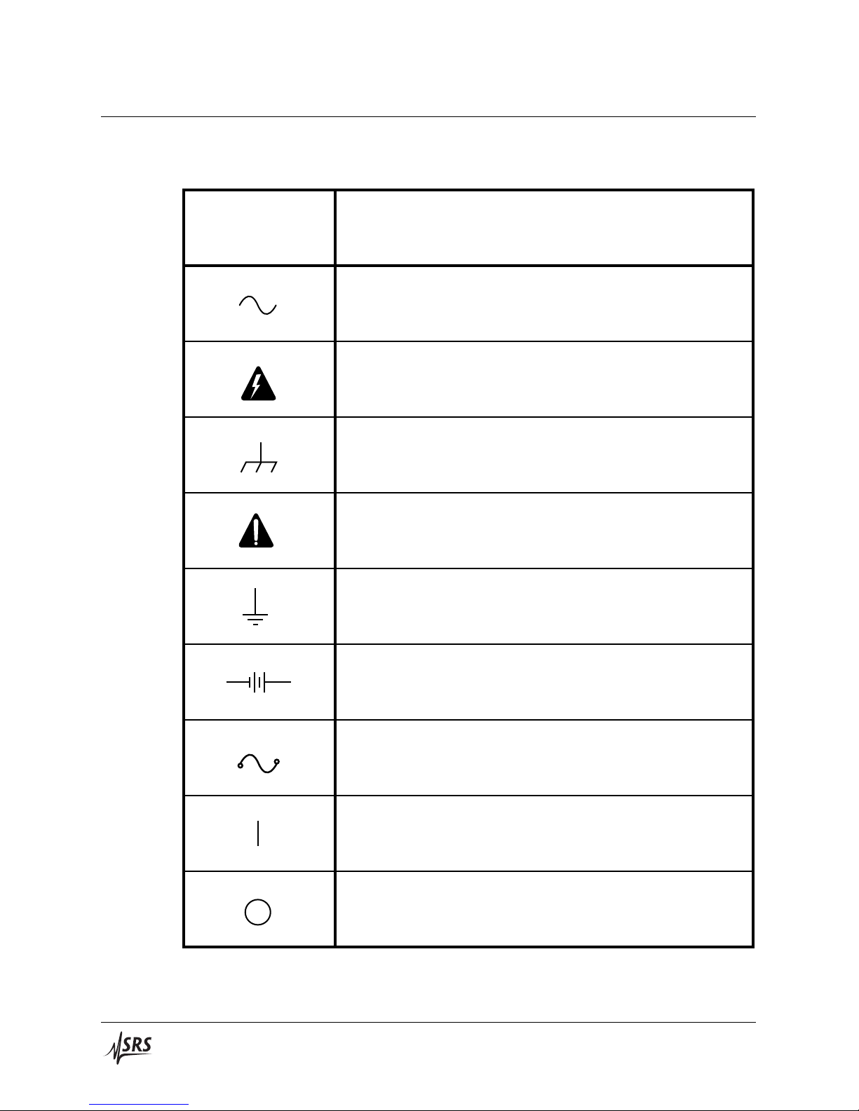
Symbol Description
Alternating current
Caution - risk of electric shock
Frame or chassis terminal
Caution - refer to accompanying documents
Earth (ground) terminal
Battery
Fuse
On (supply)
Off (supply)
Symbols you may Find on SRS Products
SIM983 Scaling Amplifier
Page 7

General Information v
Notation
The following notation will be used throughout this manual:
WARNING
CAUTION
A warning means that injury or death is possible if the instructions
are not obeyed.
A caution means that damage to the instrument or other equipment
is possible.
Typesetting conventions used in this manual are:
• Front-panel buttons are set as [gain ];
[gain ] is shorthand for “[gain ] & [gain ]”.
• Front-panel indicators are set as OVLD.
• Signal names are set as ¬STATUS.
• Signal levels are set as HIGH.
• Remote command names are set as *IDN?.
• Literal text other than command names is set as OFF.
• Special ASCII characters are set as hCRi.
Remote command examples will all be set in monospaced font. In
these examples, data sent by the host computer to the SIM983 are set
as straight teletype font, while responses received by the host
computer from the SIM983 are set as slanted teletype font.
SIM983 Scaling Amplifier
Page 8
vi General Information
Specifications
Performance characteristics
Min Typ Max Units
Input Voltage [1] −10.0 +10.0 V
Coupling DC
Resistance 0.99 1.00 1.01 MΩ
Capacitance 26 pF
Bias current [2] 40 pA
Voltage noise [3, 4], 1 kHz 43 nV/√Hz
10 kHz 38 nV/√Hz
Current noise, 10 kHz 3 fA/√Hz
Terminals Grounded BNC [5]
Gain Absolute value 0.01 19.99
Polarity Inverting, non-inverting
Resolution 0.01
Accuracy [2] ±0.01
Stability ±10 ppm/◦C
Offset [3] Voltage
Resolution, |V
| ≤ 1.999 V 1 mV
ofs
|V
| ≥ 2.00 V 10 mV
ofs
−10.00 +10.00 V
Accuracy [2, 4, 6] ±1 ± 200 mV + ppm
Stability [4] ±20 ± 20 (µV + ppm)/◦C
Settling time [7] 2 s
AC −3dB bandwidth, |G| ≤ 1.00 2.0 MHz
performance Gain-bandwidth product, |G| ≥ 1.00 3.0 MHz
[8] |G| ≥ 2.40 5.0 MHz
|G| ≥ 4.20 10.0 MHz
|G| ≥ 9.60 17.0 MHz
Slew rate 70 V/µs
THD, 1 kHz −90 dB
Output Voltage [1] −10.0 +10.0 V
Maximum current ±100 mA
Short circuit duration Indefinite
Resistance 50 Ω
Terminals Grounded BNC, front [5] and rear [9]
Operating Temperature [10] 0 40
◦
C
Power +5, ±15 V DC
Supply current, +5 V 100 mA
±15 V 300 mA
SIM983 Scaling Amplifier
Page 9

General Information vii
Conditions:
[1] An overload will be detected and the instrument is not guaranteed to
perform properly if these limits are exceeded, or if |Vin+ V
the limits. Continuous application of an input voltage Vinin excess
of ±15 V will damage the instrument.
[2] At 23◦C.
[3] Referred to input.
[4] For |G| ≥ 1. For |G| < 1, the specification applies to the output-referred
noise and offset.
[5] Amphenol 31–10–4052 or similar.
[6] Following an autocalibration at (23±5)◦C within 24 hours; following
a 2-hour warmup.
[7] To within 0.1% of the final value.
[8] The gain-bandwidth product (GBP) determines the −3 dB bandwidth:
For gain G, the bandwidth is GBP/|G|.
[9] Tyco 227169–4 or similar.
[10] Non-condensing.
|exceeds
ofs
General characteristics
Interface Serial (RS–232) through SIM interface
Connectors BNC (2 front [5], 1 rear [9]); DB–15 (male) SIM interface
Weight 1.5 lbs
Dimensions 1.500W × 3.600H × 7.000D
SIM983 Scaling Amplifier
Page 10

viii General Information
SIM983 Scaling Amplifier
Page 11

1 Getting Started
In This Chapter
This chapter gives you the necessary information to get started
quickly with your SIM983 Scaling Amplifier.
1.1 Introduction to the Instrument . . . . . . . . . . . . 1 – 2
1.1.1 Front and rear panels . . . . . . . . . . . . . . 1 – 3
1.2 Front-Panel Operation . . . . . . . . . . . . . . . . . 1 – 3
1.2.1 Polarity . . . . . . . . . . . . . . . . . . . . . 1 – 3
1.2.2 Gain . . . . . . . . . . . . . . . . . . . . . . . 1 – 3
1.2.3 Offset . . . . . . . . . . . . . . . . . . . . . . . 1 – 4
1.2.4 Overload . . . . . . . . . . . . . . . . . . . . . 1 – 4
1.3 Connections . . . . . . . . . . . . . . . . . . . . . . . 1 – 5
1.4 Power-On . . . . . . . . . . . . . . . . . . . . . . . . 1 – 6
1.5 Restoring the Default Configuration . . . . . . . . 1 – 6
1.6 SIM Interface . . . . . . . . . . . . . . . . . . . . . . 1 – 7
1.6.1 SIM interface connector . . . . . . . . . . . . 1 – 7
1.6.2 Direct interfacing . . . . . . . . . . . . . . . . 1 – 7
1 – 1
Page 12
1 – 2 Getting Started
Input BNC
1 kΩ
input protection
1.00 MΩ
High-impedance buffer
Programmable offset
Invert
noninverting
polarity
inverting
polarity
frequency
compensation
Programmable gain
(inverting)
37 Ω
13 Ω
13 Ω
Output BNC,
rear
Output BNC,
front
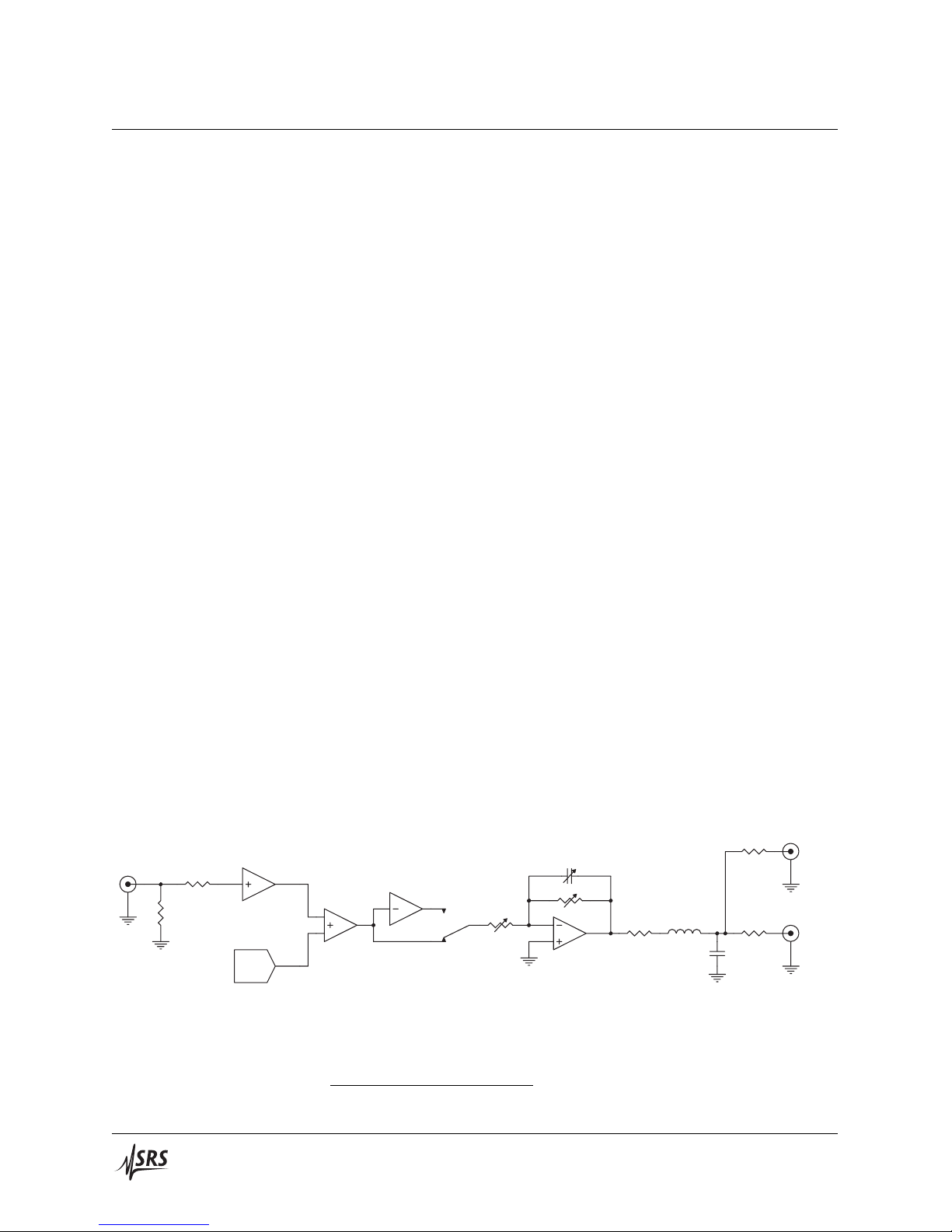
1.1 Introduction to the Instrument
The SIM983 Scaling Amplifier provides fine adjustable gain and
offset control of an analog signal. The gain (0.01 ≤ |G| ≤ 19.99),
its polarity (inverting or non-inverting), and the offset voltage
(−10.00 V ≤ V
or remotely. A remote computer can access the module through theremote interface
SIM900 Mainframe, using RS–232 or GPIB.
The digital control circuitry in the SIM983 is designed with a special
clock-stopping architecture. The microcontroller is turned on only
when the polarity, gain, or offset are being changed, during remote
communications, or when an overload condition occurs. This guarantees that no digital noise contaminates low-level analog signals.
A user-commanded autocalibration procedure allows one to controlDC accuracy
the input-referred offset to within ±1 mV of the desired value.
The amplifier’s high slew rate allows it to output a ±10 V peak-peak
sine wave at a frequency of 1 MHz. The gain stage of the amplifierAC performance
is compensated in a flexible fashion to provide a sensible pulse response, so the bandwidth of the instrument is adjusted according to
its gain.1The ample output current in the SIM983 permits one to
drive a 50 Ω load.
≤ +10.00 V) can be set from either the front panel
ofs
If the maximum input voltage is exceeded, or the gain or offset cause
the output voltage to exceed its maximum, the appropriate overload
LED turns on. If armed, the module also generates a status signal to
alert the user of the overload condition. The SIM983 can be operated
outside the SIM900 Mainframe by powering it with its required DC
voltages.
A block diagram of the amplifier is shown below in Figure 1.1.
Figure 1.1: The SIM983 block diagram.
1
The gain-bandwidth product changes with the gain.
SIM983 Scaling Amplifier
Page 13
1.2 Front-Panel Operation 1 – 3
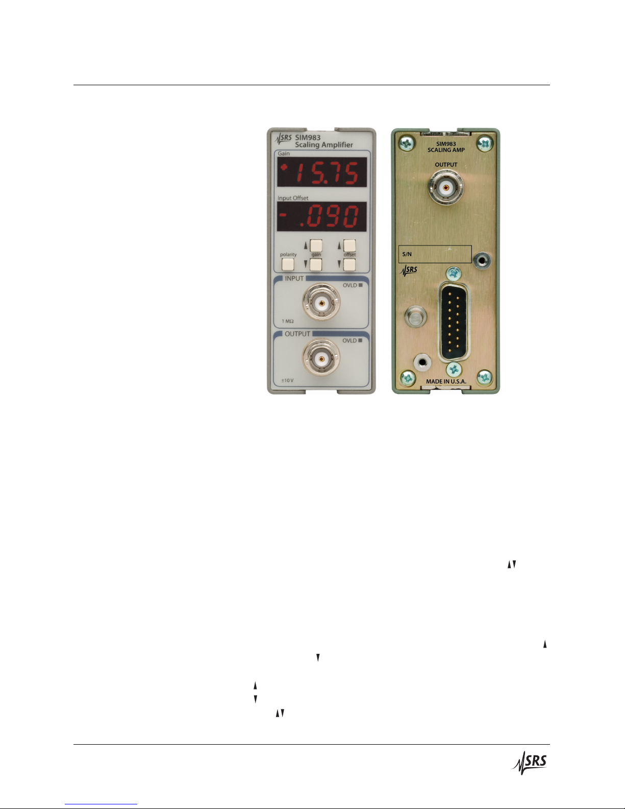
1.1.1 Front and rear panels
1.2 Front-Panel Operation
1.2.1 Polarity
The polarity is the sign of the gain. It is indicated on the upper display
of the front panel. To change the polarity, press the [polarity] button
once. Holding this button has no effect.
Pressing [polarity] has no effect on the input-referred offset. However, a simultaneous press of [polarity] and one of [gain ] has a
special meaning. This press initiates autocalibration (Section 2.2).
1.2.2 Gain
The gain G can be set to an absolute value between 0.01 and 19.99. To
raise or lower the absolute value of the gain, press the button [gain ]
or the button [gain ]. The decimal point position of the gain displayed on the front panel is fixed, so the resolution of the gain is 0.01.
If [gain ] is pressed when the gain G = ±19.99, the press has no effect.
If [gain ] is pressed when G = ±0.01, the press has no effect. Pressing
either [gain ] does not change the polarity.
Figure 1.2: The SIM983 front and rear panels.
SIM983 Scaling Amplifier
Page 14

1 – 4 Getting Started
If one of [gain ] is pressed and held, the gain is continuously adjusted. The rate of the adjustment increases as the button is held. If
the absolute value of the gain is being lowered, the rate of the adjustment changes as |G| crosses 1.00, and possibly again as |G|crosses 0.10.
If both [gain ] and [gain ] buttons are pressed at the same time, theresetting gain
absolute value of the gain is reset to 1.00. This action does not change
the polarity.
Pressing one of [gain ] and [polarity] at the same time has a special
meaning. This press initiates autocalibration (Section 2.2).
1.2.3 Offset
The input-referred voltage offset V
can be set to a value
ofs
between −10.00 V and +10.00V. Its value, in volts, is shown on
the second line of displays on the front panel of the amplifier.
To increase or decrease the offset, press the button [offset ]
or the button [offset ]. Unlike the gain, the “up” and “down”
buttons adjust the offset, not its absolute value. Thus, for
example, pressing [offset ] when V
V
= −5.48 V. If [offset ] is pressed when V
ofs
press has no effect. If [offset ] is pressed when V
= −5.49 V makes
ofs
= +10.00 V, the
ofs
= −10.00 V, the
ofs
press has no effect.
Between the values −2.00 V < V
< +2.00 V, the offset is selected
ofs
with 0.001 V resolution; the position of the decimal point on the frontpanel displays is shifted to the left. Although the resolution is 0.01 V
for |V
Thus, for example, setting V
| ≥ 2.00 V, the accuracy of the offset is still ±1 mV ± 0.02%.
ofs
= −5.48 V produces V
ofs
= (−5.480
ofs
± 0.001 ± 0.001) = (−5.480 ± 0.002) V.
If one of [offset ] is pressed and held, the offset is continuously
adjusted. The rate of the adjustment increases as the button is held.
If the value crosses the threshold V
= ±2.00 V, the rate changes
ofs
appropriately.
1.2.4 Overload
If both [offset ] and [offset ] buttons are pressed at the same time, theresetting offset
offset is reset to 0.000 V.
There are two overload indicators, one OVLD LED in the INPUT block and one OVLD LED in the OUTPUT block of the front
panel. The overload signal can also be asserted on the ¬STATUS pin.
See Section 3.5.
SIM983 Scaling Amplifier
Page 15

1.3 Connections 1 – 5
1.2.4.1 Input overload
An overload condition is recognized and the input OVLD LED is
activated if the absolute value of the voltage applied to the input
exceeds certain limits. These limits are typically ±10.0 V, and areoverload limits
between
1.2.4.2 Output overload
1.3 Connections
−10.4 V ≤ V
≤ −9.9 V, 9.9 V ≤ V
min
max
≤ 10.4 V.
The overloaded state is also recognized, and the input overload LED
activated, if the sum of the input voltage and the commanded offset,
|Vin+V
|, exceeds these limits. To distinguish between the two input
ofs
overload possibilities, use the command OVLD?. The overload LED
stays on for a minimum of 50 ms; after this time it turns off if the
overload condition has ceased.
An overload condition is recognized and the output OVLD LED is
activated if the absolute value |G × (Vin+ V
)| exceeds the limits in
ofs
Section 1.2.4.1. The overload LED stays on for a minimum of 50 ms;
after this time it turns off if the overload condition has ceased.
For a discussion of the front and rear BNC connections, see Section 2.1. The SIM interface connector is discussed in Section 1.6.1.
SIM983 Scaling Amplifier
Page 16

1 – 6 Getting Started
1.4 Power-On
The instrument retains the values of the gain and the offset in nonvolatile memory. Upon power-on, those settings are restored to their
values before the power was turned off.
The power-on configuration of the remote interface is detailed in
Section 3.3.1.
1.5 Restoring the Default Configuration
The default configuration of the SIM983 is G = +1.00, V
= 0.000 V,
ofs
and bandwidth 0 (see Section 2.3.1). This configuration is reached
from the remote interface by issuing the *RST command. To reset
only the gain or the offset to their default values, use button combinations described in Sections 1.2.2 or 1.2.3.
SIM983 Scaling Amplifier
Page 17

1.6 SIM Interface 1 – 7
1.6 SIM Interface
The primary connection to the SIM983 Scaling Amplifier is the rearpanel DB–15 SIM interface connector. Typically, the SIM983 is mated
to a SIM900 Mainframe via this connection, either through one of the
internal mainframe slots or the remote cable interface.
It is also possible to operate the SIM983 directly, without using the
SIM900 Mainframe. This section provides details on the interface.
1.6.1 SIM interface connector
The DB–15 SIM interface connector carries all the power and communication lines to the instrument. The connector signals are specified
in Table 1.1.
Direction
Pin Signal Src ⇒ Dest Description
1 SIGNAL GND MF ⇒ SIM Ground Reference 1
2 ¬STATUS SIM ⇒ MF Status/service request (GND = asserted, +5 V= idle)
3 RTS MF ⇒ SIM HW handshake (unused in SIM983)
4 CTS SIM ⇒ MF HW handshake (unused in SIM983)
5 ¬REF 10MHZ MF ⇒ SIM 10MHz reference (no connection in SIM983)
6 −5V MF ⇒ SIM Power supply (no connection in SIM983)
7 −15V MF ⇒ SIM Power supply
8 PS RTN MF ⇒ SIM Ground Reference 2
9 CHASSIS GND Chassis ground
10 TXD MF ⇒ SIM Async data (start bit = “0”= +5 V; “1” = GND)
11 RXD SIM ⇒ MF Async data (start bit = “0”= +5 V; “1” = GND)
12 +REF 10MHZ MF ⇒ SIM 10MHz reference (no connection in SIM983)
13 +5V MF ⇒ SIM Power supply
14 +15V MF ⇒ SIM Power supply
15 +24V MF ⇒ SIM Power supply (no connection in SIM983)
1.6.2 Direct interfacing
SIM983 Scaling Amplifier
Table 1.1: SIM interface connector pin assignments, DB–15.
The SIM983 is intended for operation in the SIM900 Mainframe, but
users may wish to directly interface the module to their own systems
without the use of additional hardware.
The mating connector needed is a standard DB–15 receptacle, such
as Tyco part number 747909–2 (or equivalent). Clean, well-regulated
supply voltages of ±15.0 V DC, +5.0 V DC must be provided, following the pinout specified in Table 1.1 and the minimum currents in
the table on Page vi. Ground must be provided on Pins 1 and 8, with
chassis ground on Pin 9. The ¬STATUS signal may be monitored
Page 18

1 – 8 Getting Started
on Pin 2 for a low-going TTL-compatible output indicating a status
message. See Section 3.5 for the description of status messages.
CAUTION
The SIM983 has no internal protection against reverse polarity, missing
supply, or overvoltage on the +5 V and the ±15 V power-supply pins. Supply voltages above 5.5 V on Pin 13, above +16 V on Pin 14, or below −16 V
on Pin 7 are likely to damage the instrument. SRS recommends using the
SIM983 together with the SIM900 Mainframe for most applications.
1.6.2.1 Direct interface cabling
If the user intends to directly wire the SIM983 independent of the
SIM900 Mainframe, communication is usually possible by directly
connecting the appropriate interface lines from the SIM983 DB–15
plug to the RS–232 serial port of a personal computer.2Connect RXD
from the SIM983 directly to RD on the PC, TXD directly to TD, and
similarly RTS→RTS and CTS→CTS. In other words, a null-modemstyle cable is not needed.
To interface directly to the DB–9 male (DTE) RS–232 port typically
found on contemporary personal computers, a cable must be made
with a female DB–15 socket to mate with the SIM983, and a female
DB–9 socket to mate with the PC’s serial port. Separate leads from
the DB–15 need to go to the power supply, making what is sometimes
know as a “hydra” cable. The pin connections are given in Table 1.2.
DB–15/F to SIM983 Name
DB–9/F
10 ←→3 TxD
11 ←→2 RxD
5 Computer Ground
to Power Supply
7 ←→ −15 V DC
13 ←→ +5 V DC
14 ←→ +15 V DC
1 ←→ Ground 1 (separate wire to Ground)
8 ←→ Ground 2 (separate wire to Ground)
9 ←→ Chassis Ground (separate wire to Ground)
Table 1.2: SIM983 direct interface cable pin assignments.
The distinct Ground References 1 and 2, and the chassis ground, arenote about grounds
not directly connected within the SIM983. Ground 1 carries the return
2
Although the serial interface lines on the DB–15 do not satisfy the minimum
voltage levels of the RS–232 standard, these lines are typically compatible with
desktop personal computers.
SIM983 Scaling Amplifier
Page 19

1.6 SIM Interface 1 – 9
currents of digital control signals and the power supplies, whereas
the input voltage and the output voltage reference to Ground 2 (Section 2.1.2). When operating in the SIM900, the three grounds are
tied together in the SIM900 Mainframe. Grounds 1 and 2 are connected through back-to-back Schottky diodes, so they cannot be more
than ∼ ±0.35 V apart. The three ground lines should be separately
wired to a single, low-impedance ground source at the power supply.
1.6.2.2 Serial settings
The initial serial port settings at power-on are: baud rate 9600, 8 bits,
no parity, 1 stop bit, and no flow control. The baud rate of the SIM983
cannot be changed. Flow control is not implemented in the SIM983.
The parity may be changed with the PARI command.
SIM983 Scaling Amplifier
Page 20

1 – 10 Getting Started
SIM983 Scaling Amplifier
Page 21

2 Description of Operation
This chapter provides a number of additional details of the operation
of the SIM983.
In This Chapter
2.1 Signal Connections and Grounding . . . . . . . . . 2 – 2
2.2 Autocalibration . . . . . . . . . . . . . . . . . . . . . 2 – 2
2.3 AC Characteristics . . . . . . . . . . . . . . . . . . . 2 – 3
2.4 Clock Stopping . . . . . . . . . . . . . . . . . . . . . 2 – 4
2.1.1 Output drive . . . . . . . . . . . . . . . . . . 2 – 2
2.1.2 Grounds . . . . . . . . . . . . . . . . . . . . . 2 – 2
2.3.1 Bandwidth . . . . . . . . . . . . . . . . . . . . 2 – 3
2.3.2 Slew rate . . . . . . . . . . . . . . . . . . . . . 2 – 3
2 – 1
Page 22

2 – 2 Description of Operation
2.1 Signal Connections and Grounding
2.1.1 Output drive
The output impedance of the SIM983 Scaling Amplifier is 50 Ω.
The amplifier can drive load impedances from ∞ to 50 Ω for the
full ±10 V range of output voltage. When driving a 50 Ω load, the
gain will be half of that displayed on the front panel.
The rear-panel output connector is wired in parallel with the frontpanel output, and shares some of the output impedance (Figure 1.1).
The output stage is not designed to drive two 50 Ω loads simultaneously.
2.1.2 Grounds
Both the input and the output of the SIM983 are referenced to ground.
To maintain the DC accuracy of the instrument, there are two separate ground references. Ground 1 (Pin 1 of the SIM interface connector) provides a return path for digital control signals and the power
supply currents, while Ground 2 (Pin 8 of the interface connector)
serves as the reference point for analog voltages. The outer casings
of the input and the output front-panel BNC connectors are tied to
Ground 2. The output current of the amplifier returns to the power
supply through Ground 2.
2.2 Autocalibration
The outer casing of the rear-panel output BNC is connected to chassis ground, Pin 9 of the DB–15 SIM interface connector. The separate power, analog, and chassis grounds are not directly connected
within the amplifier. When operating in the SIM900 Mainframe, the
three grounds are tied together inside the mainframe, and through
the mainframe to the Earth. Grounds 1 and 2 are connected inside
the SIM983 through back-to-back Schottky diodes, so they cannot be
more than ∼ ±0.35 V apart.
To ensure DC offset accuracy, the amplifier must be self-calibrated
within the 24 hours preceding a measurement. A valid autocalibration must take place at (23 ± 5)◦C with the module warmed up
for at least 2 hours at (23 ± 5)◦C. If the module is being used inside the SIM900 Mainframe, the autocalibration must also be inside
the mainframe. Otherwise, perform the autocalibration with the
same connection to an independent supply as you use for the operation. The autocalibration is only accurate if the output has stabilized
within ±15 mV of zero for at least 2 minutes immediately preceding the calibration. However, the gain and the offset need not be at
SIM983 Scaling Amplifier
Page 23

2.3 AC Characteristics 2 – 3
their default values; after the calibration completes, these values are
restored.
Disconnect all inputs and outputs to the SIM983 while performing the au-
tocalibration. To calibrate, issue the command ACAL, or press the but-
ton [polarity] and one of [gain ] at the same time. The calibration
completes and the instrument is ready for operation within 2 seconds. If autocalibration is unsuccessful, for example because an
external voltage (which cannot be nulled) is applied to the input, the
calibration parameters revert to their original values and the com-
mand LDDE? will return Code 1.
Autocalibration does not affect gain accuracy.
2.3 AC Characteristics
2.3.1 Bandwidth
The gain-bandwidth product (GBP) of the SIM983 is a measure of
its small-signal behavior, and depends on |G|. Four gain ranges
correspond to four values of gain-bandwidth product, as specified in the table on Page vi. For |G| ≥ 1, the −3 dB small-signal
bandwidth of the amplifier is f
f
−3 dB
(G) & f
(G = 1.00).
−3 dB
= GBP/|G|. For |G| < 1,
−3 dB
2.3.2 Slew rate
The gain-bandwidth product is determined by a compensation capacitor in the feedback path of the gain-stage amplifier. It is possible
to override the value of this capacitor, giving the instrument more
bandwidth. To do this, use the command BWTH. If the bandwidth
is altered in this way, the next front-panel button press will return
the bandwidth to the value appropriate for the current gain. Cycling the power or performing an autocalibration will also return the
bandwidth to its default value for the gain.
If the bandwidth is set to a value other than its default, the amplifier may
exhibit slow settling, excessive ringing, or oscillations.
The small-signal settling time of the amplifier is a complex function
of its gain and its bandwidth.
The slew rate of an amplifier is a measure of its large-signal behavior. It is the maximum rate of change of the output voltage,
measured in V/s. The slew rate (SR) determines the maximum undistorted AC signal that can be output; for a sine-wave output at a frequency f , the maximum peak-peak voltage is |V
max−Vmin
| = SR/(π f ).
The SIM983 is designed to be able to output a full-range sine wave
at 1 MHz.
SIM983 Scaling Amplifier
Page 24

2 – 4 Description of Operation
If the output or an intermediate stage of the amplifier is driven beyond the
limits in the table on Page vi, large-signal behavior is not guaranteed.
2.4 Clock Stopping
The microprocessor clock of the SIM983 stops if the module is idle,
“freezing” the digital circuitry. The following actions “wake up” the
clock:
1. A power-on.
2. A press of a front-panel button.
3. Activity (send or receive) at the remote interface.
4. An overload.
The clock runs for as long as is necessary to complete a gain or offset
adjustment, or to communicate the output of a query through the
remote interface. However, the clock will remain active for as long
as the overload condition exists.
This default behavior can be modified with the remote com-
mand AWAK. Setting AWAKON will prevent the clock from stopping.
The module returns to AWAKOFF upon power-on.
SIM983 Scaling Amplifier
Page 25

3 Remote Operation
In This Chapter
This chapter describes operating the SIM983 over the serial interface.
3.1 Index of Common Commands . . . . . . . . . . . . 3 – 2
3.2 Alphabetic List of Commands . . . . . . . . . . . . 3 – 4
3.3 Introduction . . . . . . . . . . . . . . . . . . . . . . . 3 – 6
3.3.1 Power-on configuration . . . . . . . . . . . . 3 – 6
3.3.2 Buffers . . . . . . . . . . . . . . . . . . . . . . 3 – 6
3.3.3 Device Clear . . . . . . . . . . . . . . . . . . . 3 – 6
3.4 Commands . . . . . . . . . . . . . . . . . . . . . . . 3 – 7
3.4.1 Command syntax . . . . . . . . . . . . . . . . 3 – 7
3.4.2 Notation . . . . . . . . . . . . . . . . . . . . . 3 – 8
3.4.3 Examples . . . . . . . . . . . . . . . . . . . . 3 – 8
3.4.4 General commands . . . . . . . . . . . . . . . 3 – 9
3.4.5 Configuration commands . . . . . . . . . . . 3 – 10
3.4.6 Calibration commands . . . . . . . . . . . . . 3 – 11
3.4.7 Status commands . . . . . . . . . . . . . . . . 3 – 11
3.4.8 Interface commands . . . . . . . . . . . . . . 3 – 14
3.4.9 Serial communication commands . . . . . . 3 – 17
3.5 Status Model . . . . . . . . . . . . . . . . . . . . . . 3 – 19
3.5.1 Status Byte (SB) . . . . . . . . . . . . . . . . . 3 – 20
3.5.2 Service Request Enable (SRE) . . . . . . . . . 3 – 20
3.5.3 Standard Event Status (ESR) . . . . . . . . . 3 – 20
3.5.4 Standard Event Status Enable (ESE) . . . . . 3 – 21
3.5.5 Communication Error Status (CESR) . . . . . 3 – 21
3.5.6 Communication Error Status Enable (CESE) 3 – 22
3.5.7 Overload Status (OLSR) . . . . . . . . . . . . 3 – 22
3.5.8 Overload Status Enable (OLSE) . . . . . . . . 3 – 23
3 – 1
Page 26

3 – 2 Remote Operation
3.1 Index of Common Commands
Symbol Definition
f Floating-point value
i Bit number (0–7)
j Unsigned integer (0–255)
m Unsigned integer (0–3)
z Literal token
(?) Required for queries; illegal for set commands
var Parameter always required
{var} Required parameter for set commands; illegal for queries
[var] Optional parameter for both set and query forms
General
HELP(?) 3 – 9 Instrument Help
AWAK(?) {z} 3 – 10 Keep Clock Awake
Configuration
GAIN(?) {f } 3 – 10 Gain
OFST(?) {f } 3 – 10 Offset
BWTH(?) [m] 3 – 11 Bandwidth
Calibration
ACAL 3 – 11 Autocalibration
Status
*CLS 3 – 11 Clear Status
*STB? [i] 3 – 12 Status Byte
*SRE(?) [i,] {j} 3 – 12 Service Request Enable
*ESR? [i] 3 – 12 Standard Event Status
*ESE(?) [i,] {j} 3 – 12 Standard Event Status Enable
CESR? [i] 3 – 12 Communication Error Status
CESE(?) [i,] {j} 3 – 13 Communication Error Status Enable
OLSR? [i] 3 – 13 Overload Status
OLSE(?) [i,] {j} 3 – 13 Overload Status Enable
PSTA(?) {z} 3 – 13 Pulse ¬STATUS Mode
LBTN? 3 – 13 Last Button
OVLD? 3 – 14 Overload
Interface
*RST 3 – 14 Reset
*IDN? 3 – 15 Identify
*TST? 3 – 15 Self Test
SIM983 Scaling Amplifier
Page 27

3.1 Index of Common Commands 3 – 3
*OPC(?) 3 – 15 Operation Complete
CONS(?) {z} 3 – 15 Console Mode
LEXE? 3 – 16 Execution Error
LCME? 3 – 16 Command Error
LDDE? 3 – 17 Device Error
TOKN(?) {z} 3 – 17 Token Mode
TERM(?) {z} 3 – 17 Response Termination
Serial Communications
PARI(?) {z} 3 – 18 Parity
SIM983 Scaling Amplifier
Page 28

3 – 4 Remote Operation
3.2 Alphabetic List of Commands
?
*CLS 3 – 11 Clear Status
*ESE(?) [i,] {j} 3 – 12 Standard Event Status Enable
*ESR? [i] 3 – 12 Standard Event Status
*IDN? 3 – 15 Identify
*OPC(?) 3 – 15 Operation Complete
*RST 3 – 14 Reset
*SRE(?) [i,] {j} 3 – 12 Service Request Enable
*STB? [i] 3 – 12 Status Byte
*TST? 3 – 15 Self Test
A
ACAL 3 – 11 Autocalibration
AWAK(?) {z} 3 – 10 Keep Clock Awake
B
BWTH(?) [m] 3 – 11 Bandwidth
C
CESE(?) [i,] {j} 3 – 13 Communication Error Status Enable
CESR? [i] 3 – 12 Communication Error Status
CONS(?) {z} 3 – 15 Console Mode
G
GAIN(?) {f } 3 – 10 Gain
H
HELP(?) 3 – 9 Instrument Help
L
LBTN? 3 – 13 Last Button
LCME? 3 – 16 Command Error
LDDE? 3 – 17 Device Error
LEXE? 3 – 16 Execution Error
O
OFST(?) {f } 3 – 10 Offset
OLSE(?) [i,] {j} 3 – 13 Overload Status Enable
OLSR? [i] 3 – 13 Overload Status
OVLD? 3 – 14 Overload
SIM983 Scaling Amplifier
Page 29

3.2 Alphabetic List of Commands 3 – 5
P
PARI(?) {z} 3 – 18 Parity
PSTA(?) {z} 3 – 13 Pulse ¬STATUS Mode
T
TERM(?) {z} 3 – 17 Response Termination
TOKN(?) {z} 3 – 17 Token Mode
SIM983 Scaling Amplifier
Page 30

3 – 6 Remote Operation
3.3 Introduction
Remote operation of the SIM983 is through a simple command language documented in this chapter. Both set and query forms of most
commands are supported, allowing the user complete control of the
amplifier from a remote computer, either through the SIM900 Mainframe or directly via RS–232 (see Section 1.6.2.1).
See Table 1.1 for the specification of the DB–15 SIM Interface Connector.
3.3.1 Power-on configuration
The initial settings for the remote interface are 9600 baud with no
parity and no flow control, and with local echo disabled (CONS OFF).
The values of the gain and the offset are retained in non-volatile
memory. Upon power-on, those settings are restored to their values
before the power was turned off. The bandwidth is set to the value
appropriate for the stored gain.
Where appropriate, the default or power-on value for parameters is
listed in boldface in the command descriptions.
3.3.2 Buffers
3.3.3 Device Clear
The SIM983 stores incoming bytes from the host interface in a 64byte input buffer. Characters accumulate in the input buffer until
a command terminator (either hCRi or hLFi) is received, at which
point the message is parsed and executed. Query responses from
the SIM983 are buffered in a 64-byte output queue.
If the input buffer overflows, then all data in both the input buffer
and the output queue are discarded, and an error is recorded in the
CESR and ESR status registers.
The SIM983 host interface can be asynchronously reset to its poweron configuration by sending an RS–232-style hbreakisignal. From the
SIM900 Mainframe, this is accomplished with the SRST command;
if directly interfacing via RS–232, then use a serial break signal. After
receiving the Device Clear, the CONS mode is turned OFF. Note that
this only resets the communication interface; the basic function of
the SIM983 is left unchanged; to reset the amplifier, use *RST.
The Device Clear signal will also terminate the output of the HELP?
command from the SIM983.
SIM983 Scaling Amplifier
Page 31

3.4 Commands 3 – 7
3.4 Commands
This section provides syntax and operational descriptions for remote
commands.
3.4.1 Command syntax
The four letter mnemonic (shown in CAPS) in each command se-
quence specifies the command. The rest of the sequence consists of
parameters.
Commands may take either set or query form, depending on whether
the “?” character follows the mnemonic. Set only commands are
listed without the “?”, query only commands show the “?” after the
mnemonic, and optionally query commands are marked with a “(?)”.
Parameters shown in { } and [ ] are not always required. Parameters
in { } are required to set a value, and should be omitted for queries.
Parameters in [ ] are optional in both set and query commands. Parameters listed without surrounding characters are always required.
Do not send ( ) or { } or [ ] as part of the command.
Multiple parameters are separated by commas. Multiple commands
may be sent on one command line by separating them with semicolons (;) so long as the input buffer does not overflow. Commands
are terminated by either hCRi or hLFi characters. Null commands
and whitespaces are ignored. Execution of the command does not
begin until the command terminator is received.
Token parameters (generically shown as z in the command descrip-tokens
tions) can be specified either as a keyword or as an integer value.
Command descriptions list the valid keyword options, with each
keyword followed by its corresponding integer value. For example,
to set the response termination sequence to hCRi+hLFi, the following
two commands are equivalent:
TERM CRLF —or— TERM 3
For queries that return token values, the return format (keyword or
integer) is specified with the TOKN command.
SIM983 Scaling Amplifier
Page 32

3 – 8 Remote Operation
3.4.2 Notation
The following table summarizes the notation used in the command
descriptions:
Symbol Definition
f Floating-point value
i Bit number (0–7)
j Unsigned integer (0–255)
m Unsigned integer (0–3)
z Literal token
(?) Required for queries; illegal for set commands
var Parameter always required
{var} Required parameter for set commands; illegal for queries
[var] Optional parameter for both set and query forms
3.4.3 Examples
Each command is provided with a simple example illustrating its
usage. In these examples, all data sent by the host computer to
the SIM983 are set as straight teletype font, while responses
received by the host computer from the SIM983 are set as slanted
teletype font.
The usage examples vary with respect to set/query, optional parameters, and token formats. These examples are not exhaustive, and are
intended to provide a convenient starting point for user programming.
SIM983 Scaling Amplifier
Page 33

3.4 Commands 3 – 9
3.4.4 General commands
Instrument HelpHELP(?)
Outputs a condensed version of Section 3.4 to the remote interface.
HELP may be used with or without the query sign, with the same
effects.
HELP?Example:
Notation:
f is a floating-point number;
i is bit number (0..7);
j is an 8-bit unsigned integer (0..255);
m is a 2-bit unsigned integer (0..3);
z is a token
(?) question required for queries, illegal for set commands;
[] = parameter is optional for both set and query forms;
{} = parameter is required to set, illegal for queries;
parameter without brackets is always required;
the brackets themselves should not be sent.
General commands:
HELP? - Send this text.
AWAK(?) {z} - Keep the module clock awake.
Configuration commands:
GAIN(?) {f} - Set/query gain.
OFST(?) {f} - Set/query offset.
BWTH(?) [m] - Output bandwidth.
Calibration commands:
ACAL - One-time autocalibration.
Status commands:
*CLS - Clear Status.
*STB? [i] - Query the Status Byte.
*SRE(?) [i,] {j} - Service Request Enable.
*ESR? [i] - Query Standard Event Status register.
*ESE(?) [i,] {j} - Standard Event Status Enable.
CESR? [i] - Query the Communications Error Status.
CESE(?) [i,] {j} - Communications Error Status Enable.
OLSR? [i] - Query Overload Status register.
OLSE(?) [i,] {j} - Overload Status Enable.
PSTA(?) {z} - Pulse Status or change its level.
LBTN? - Which button last pressed?
OVLD? - Input or output currently overloaded?
SIM983 Scaling Amplifier
Page 34

3 – 10 Remote Operation
Interface commands:
*RST - Reset to known state.
*IDN? - Identify.
*TST? - Does nothing.
*OPC(?) - Operation complete.
CONS(?) {z} - Console OFF/ON.
LEXE? - Last Execution Error.
LCME? - Last Communications Error.
LDDE? - Last Device-Dependent Error.
TOKN(?) {z} - Turn token mode OFF/ON.
TERM(?) {z} - Cmd line end (NONE, CR, LF, CRLF, LFCR).
Serial interface command (baud rate is always 9600):
PARI(?) {z} - Parity (NONE, EVEN, ODD, MARK, SPACE).
Keep Clock AwakeAWAK(?) {z}
Set (query) the SIM983 keep-awake mode {to z = (OFF 0, ON 1)}.
Ordinarily, the clock oscillator for the SIM983 microcontroller is held
in a stopped state, and only enabled during processing of events
(Section 2.4). Setting AWAK ON forces the clock to stay running, and
is useful only for diagnostic purposes.
AWAK ONExample:
3.4.5 Configuration commands
GainGAIN(?) {f }
Set (query) the amplifier gain {to f}. The module accepts signed
floating-point values in the ranges −19.99 ≤ f ≤ −0.01, 0.01 ≤ f
≤ 19.99. The reset value is f = +1.00 .
After a GAIN set command, the bandwidth is set to the value appro-
priate for the new gain. Gain queries do not alter the bandwidth.
GAIN 1.4232E1; GAIN?Example:
+14.23
OffsetOFST(?) {f }
Set (query) the offset of the amplifier {to f volts}. The module accepts
signed floating-point values in the range −10.000 ≤ f ≤ 10.000. The
reset value is f = 0.000 .
Setting or querying the offset does not change the bandwidth.
SIM983 Scaling Amplifier
Page 35

3.4 Commands 3 – 11
OFST -7.032; OFST?Example:
-07.030
BandwidthBWTH(?) [m]
Set (query) the gain-bandwidth product of the amplifier [to m]. Allowed values of the optional parameter are 0 through 3, with a larger
value corresponding to a greater gain-bandwidth. When the gain is
set from the front panel or from the remote interface, the bandwidth
automatically reverts to the following:
Range Bandwidth m GBP, MHz min
0.01 ≤ |G| ≤ 2.39 0 3.0 (|G| ≥ 1.00)
2.40 ≤ |G| ≤ 4.19 1 5.0
4.20 ≤ |G| ≤ 9.59 2 10.0
9.60 ≤ |G| ≤ 19.99 3 17.0
The bandwidth is also automatically selected from this table if the
optional parameter is omitted.
GAIN 17; BWTH 1; BWTH?Example:
1
GAIN 17; BWTH?
3
3.4.6 Calibration commands
AutocalibrationACAL
Perform a self-calibration (Section 2.2). Make sure to disconnect all
inputs and outputs to the SIM983, and to set the output to zero. Remote
commands are not processed until ACAL is complete.
ACALExample:
LDDE?
0
checks for success of an autocalibration.
3.4.7 Status commands
The Status commands query and configure registers associated with
status reporting of the SIM983. See Section 3.5 for the status model.
Clear Status*CLS
*CLS immediately clears the ESR, CESR, and OLSR status registers.
*CLSExample:
SIM983 Scaling Amplifier
Page 36

3 – 12 Remote Operation
Status Byte*STB? [i]
Query the Status Byte register [Bit i].
Execution of the *STB? query (without the optional Bit i) always
causes the ¬STATUS signal to be deasserted. Note that *STB? i will
not clear ¬STATUS, even if Bit i is the only bit presently causing the
¬STATUS signal.
*STB?Example:
16
Service Request Enable*SRE(?) [i,] {j}
Set (query) the Service Request Enable register [Bit i] {to j}.
*SRE 0,1Example:
Standard Event Status*ESR? [i]
Query the Standard Event Status Register [Bit i].
Upon execution of *ESR?, the returned bit(s) of the ESR register are
cleared.
*ESR?Example:
64
Standard Event Status Enable*ESE(?) [i,] {j}
Set (query) the Standard Event Status Enable register [Bit i] {to j}.
*ESE 6,1Example:
ESE?
64
Communication Error StatusCESR? [i]
Query the Communication Error Status Register [Bit i].
Upon executing a CESR? query, the returned bit(s) of the CESR reg-
ister are cleared.
CESR?Example:
0
SIM983 Scaling Amplifier
Page 37

3.4 Commands 3 – 13
Communication Error Status EnableCESE(?) [i,] {j}
Set (query) the Communication Error Status Enable register [Bit i]
{to j}.
CESE?Example:
2
Overload StatusOLSR? [i]
Query the Overload Status Register [Bit i].
Upon executing an OLSR? query, the returned bit(s) of the OLSR reg-
ister are cleared.
OLSR?Example:
3
Overload Status EnableOLSE(?) [i,] {j}
Set (query) the Overload Status Enable register [Bit i] {to j}.
OLSE 4Example:
Pulse ¬STATUS ModePSTA(?) {z}
Set (query) the Pulse ¬STATUS mode {to z = (OFF 0, ON 1)}.
When PSTA ON is set, all new service requests will only pulse the
¬STATUS signal LOW (for a minimum of 1 µs). The default behavior
is to latch ¬STATUS LOW until a *STB? query is received.
A reset does not alter PSTA. The value in boldface above is the
power-on value.
PSTA?Example:
OFF
Last ButtonLBTN?
Query the number of the last button pressed. The response is
LBTN? Last button
1 [polarity]
2 [gain ]
3 [gain ]
4 [offset ]
5 [offset ]
6 Both [gain ] and [gain ] (reset gain)
7 Both [offset ] and [offset ] (reset offset)
8 One of [gain ] and [polarity] (autocalibrate)
SIM983 Scaling Amplifier
Page 38

3 – 14 Remote Operation
The value 0 is returned if no button was pressed since the last LBTN?.
A query of LBTN? always clears the button code, so a subse-
quent LBTN? will return 0.
LBTN?Example:
5
OverloadOVLD?
Query the current overload condition. The response is
OVLD? Overloaded
1 Input
2 Input + offset
4 Output
Combination overloads are reported by summing the values of the individual overload flags. This command complements the OLSR status register described in Section 3.5.7, and the three overload flags
correspond one-to-one with bits in OLSR. However, once cleared
by OLSR? or *CLS, the overload status bits will stay cleared even
though the overload condition may persist and remain reported
by OVLD?.
3.4.8 Interface commands
OVLD?Example:
6
implies that the input is not overloaded; the intermediate stage
(Vin+ V
) is overloaded; and the output is overloaded.
ofs
The Interface commands provide control over the interface between
the SIM983 and the host computer.
Reset*RST
Reset the SIM983 to its default configuration.
*RST sets the following:
• Clock oscillator to stop during idle time (AWAKOFF).
• Gain to +1.00.
• Offset to 0.000 V.
• Bandwidth to 0.
• The token mode to OFF.
*RST does not affect PSTA, CONS, TERM, and all service-enable
registers (*SRE, *ESE, CESE, or OLSE).
SIM983 Scaling Amplifier
Page 39

3.4 Commands 3 – 15
*RSTExample:
CONS?
1
Identify*IDN?
Query the device identification string.
The identification string is formatted as:
Stanford Research Systems,SIM983,s/n******,ver#.###
where SIM983 is the model number, ****** is a 6-digit serial number,
and #.### is the firmware revision level.
*IDN?Example:
Stanford Research Systems,SIM983,s/n004900,ver2.0
Self Test*TST?
There is no internal self-test in the SIM983 after the power-on, so this
query always returns 0.
*TST?Example:
0
Operation Complete*OPC(?)
Sets the OPC flag in the ESR register.
The query form *OPC? writes a 1 into the output queue when com-
plete, but does not affect the ESR register.
*OPC?Example:
1
Console ModeCONS(?) {z}
Set (query) the console mode {to z = (OFF 0, ON 1)}.
CONScauses each character received at the input buffer to be copied
to the output queue.
A reset does not alter CONS. The value in boldface above is the
power-on value. CONSis set to OFF upon Device Clear.
CONS ONExample:
SIM983 Scaling Amplifier
Page 40

3 – 16 Remote Operation
Execution ErrorLEXE?
Query the Last Execution Error code. A query of LEXE? always
clears the error code, so a subsequent LEXE? will return 0. Valid
codes are:
Value Definition
0 No execution error since last LEXE?
1 Illegal value
2 Wrong token
3 Invalid bit
*STB? 12; LEXE?; LEXE?Example:
3
0
The error (3, ”Invalid bit”) is because *STB? only allows bit-specific
queries of 0–7. The second read of LEXE? returns 0.
Command ErrorLCME?
Query the Last Command Error code. A query of LCME? always
clears the error code, so a subsequent LCME? will return 0. Valid
codes are:
Value
Definition
0 No command error since last LCME?
1 Illegal command
2 Undefined command
3 Illegal query
4 Illegal set
5 Missing parameter(s)
6 Extra parameter(s)
7 Null parameter(s)
8 Parameter buffer overflow
9 Bad floating point
10 Bad integer
11 Bad integer token
12 Bad token value
14 Unknown token
*IDNExample:
LCME?
4
The error (4, ”Illegal set”) is due to the missing “?”.
SIM983 Scaling Amplifier
Page 41

3.4 Commands 3 – 17
Device ErrorLDDE?
Query the Last Device-Dependent Error code. A query of LDDE?
always clears the error code, so a subsequent LDDE? will return 0.
Valid codes are:
Value Definition
0 No execution error since last LEXE?
1 Unable to autocalibrate
ACALExample:
LDDE?
0
indicates a successful autocalibration.
Token ModeTOKN(?) {z}
Set (query) the token query mode {to z = (OFF 0, ON 1)}.
If TOKN ON is set, then queries to the SIM983 that return tokens will
return a text keyword; otherwise they return a decimal integer value.
Thus, the only possible responses to the TOKN?query are ON and 0.
TOKN OFFExample:
Response TerminationTERM(?) {z}
Set (query) the htermi sequence {to z = (NONE 0, CR 1, LF 2, CRLF 3,
or LFCR 4)}.
The htermi sequence is appended to all query responses sent by
the module, and is constructed of ASCII character(s) 13 (carriage
return) and 10 (line feed). The token mnemonic gives the sequence
of characters.
A reset does not alter TERM. The value in boldface above is the
power-on value.
TOKN ON; TERM?Example:
CRLF
3.4.9 Serial communication commands
Note that the SIM983 can only support a single baud rate of 9600,
and does not support flow control. A reset does not change the serial
interface settings; use Device Clear.
SIM983 Scaling Amplifier
Page 42

3 – 18 Remote Operation
ParityPARI(?) {z}
Set (query) the parity {to z = (NONE 0, ODD 1, EVEN 2, MARK 3,
SPACE 4)}. The value in boldface is the power-on value.
TOKN ON; PARI?Example:
EVEN
SIM983 Scaling Amplifier
Page 43

3.5 Status Model 3 – 19
7
X
5
4
3
2
1
0
CESB
MSS
ESB
IDLE
undef
undef
undef
OLSB
7
6
5
4
3
2
1
0
Status Byte
SB SRE
7
6
5
4
3
2
1
0
7
6
5
4
3
2
1
0
OPC: Operation Complete
INP: Input Buffer Error
DDE: Device Error
EXE: Execution Error
CME: Command Error
URQ: User Request
PON: Power On
QYE: Query Error
ESR ESE
Standard Event Status
7
6
5
4
3
2
1
0
7
6
5
4
3
2
1
0
PARITY: Parity Error
FRAME: Framing Error
HWOVRN: Hardware Input Overrun
OVR: Input Buffer Overrun
RTSH: RTS Halted
CTSH: CTS Halted
DCAS: Device Clear
NOISE: Noise Error
CESR CESE
Communication Error Status
X
X
X
X
X
2
1
0
X
X
X
X
X
2
1
0
Input
Input + Offset
undef
undef
undef
undef
undef
Output
OLSR OLSE
Overload Status
-
STATUS
3.5 Status Model
The SIM983 status registers follow the hierarchical IEEE–488.2 for-status registers
mat. A block diagram of the status register array is given in Figure 3.1.
Event Registers : These read-only registers record the occurrence of defined
SIM983 Scaling Amplifier
Enable Registers : These read/write registers define a bitwise mask for their cor-
Figure 3.1: Status register model for the SIM983 Scaling Amplifier.
There are two categories of registers in the SIM983 status model:
events. If the event occurs, the corresponding bit is set to 1.
Upon querying an event register, all set bits within it are
cleared. These are sometimes known as “sticky bits,” since
once set, a bit can only be cleared by reading its value. Event
register names end with SR.
responding event register. If a bit position is set in an event
register while the same bit position is also set in the enable
register, then the corresponding summary bit message is set.
Enable register names end with SE.
Page 44

3 – 20 Remote Operation
At power-on, all status registers are cleared.
3.5.1 Status Byte (SB)
The Status Byte is the top-level summary of the SIM983 status model.
When masked by the Service Request Enable register, a bit set in the
Status Byte causes the ¬STATUS signal to be asserted on the rearpanel SIM interface connector.
Weight Bit Flag
1 0 OLSB
2 1 undef (0)
4 2 undef (0)
8 3 undef (0)
16 4 IDLE
32 5 ESB
64 6 MSS
128 7 CESB
OLSB : Overload Summary Bit. Indicates whether one or more of the
enabled flags in the Overload Status Register has become true.
IDLE : Indicates that the input buffer is empty and the command
parser is idle. Can be used to help synchronize SIM983 query
responses.
ESB : Event Status Bit. Indicates whether one or more of the enabled
events in the Standard Event Status Register is true.
MSS : Master Summary Status. Indicates whether one or more of the
enabled status messages in the Status Byte register is true.
CESB : Communication Error Summary Bit. Indicates whether one or
more of the enabled flags in the Communication Error Status
Register has become true.
3.5.2 Service Request Enable (SRE)
Each bit in the SRE corresponds one-to-one with a bit in the SB register, and acts as a bitwise AND of the SB flags to generate MSS. Bit 6 of
the SRE is undefined—setting it has no effect, and reading it always
returns 0. This register is set and queried with the *SRE(?)command.
At power-on, this register is cleared.
3.5.3 Standard Event Status (ESR)
The Standard Event Status Register consists of 8 event flags. These
event flags are all “sticky bits” that are set by the corresponding
events, and cleared only by reading or with the *CLS command.
Reading a single bit (with the *ESR? i query) clears only Bit i.
SIM983 Scaling Amplifier
Page 45

3.5 Status Model 3 – 21
Weight Bit Flag
1 0 OPC
2 1 INP
4 2 QYE
8 3 DDE
16 4 EXE
32 5 CME
64 6 URQ
128 7 PON
OPC : Operation Complete. Set by the *OPC command.
INP : Input buffer error. Indicates data has been discarded from the
input buffer.
QYE : Query Error. Indicates data in the output queue has been lost.
DDE : Device-Dependent Error. Indicates a failed autocalibration.
EXE : Execution Error. Indicates the error in a command that was
successfully parsed. Out-of-range parameters are an example.
CME : Command Error. Indicates a command parser-detected error.
URQ : User Request. Indicates that a front-panel button was pressed.
PON : Power On. Indicates that an off-to-on transition has occurred.
3.5.4 Standard Event Status Enable (ESE)
The ESE acts as a bitwise AND with the ESR register to produce the
single-bit ESB message in the Status Byte Register (SB). The register
can be set and queried with the *ESE(?) command.
At power-on, this register is cleared.
3.5.5 Communication Error Status (CESR)
The Communication Error Status Register consists of 8 event flags;
each of the flags is set by the corresponding event, and cleared only
by reading the register or with the *CLS command. Reading a single
bit (with the CESR? i query) clears only Bit i.
Weight Bit Flag
1 0 PARITY
2 1 FRAME
4 2 NOISE
8 3 HWOVRN
16 4 OVR
32 5 RTSH
64 6 CTSH
128 7 DCAS
SIM983 Scaling Amplifier
Page 46

3 – 22 Remote Operation
PARITY : Parity error. Set by serial parity mismatch on the incoming data
byte.
FRAME : Framing error. Set when an incoming serial data byte is missing
the STOP bit.
NOISE : Noise error. Set when an incoming serial data byte does not
present a steady logic level during each asynchronous bitperiod window.
HWOVRN : Hardware Overrun. Set when an incoming serial data byte is
lost due to internal processor latency. Causes the input buffer
to be flushed, and resets the command parser.
OVR : Input buffer Overrun. Set when the input buffer is overrun by
the incoming data. Causes the input buffer to be flushed, and
resets the command parser.
RTSH : RTS Holdoff Event. Unused in the SIM983.
CTSH : CTS Holdoff Event. Unused in the SIM983.
DCAS : Device Clear. Indicates that the SIM983 received the Device
Clear signal (an RS–232 hbreaki). Clears the input buffer and
the output queue, and resets the command parser.
3.5.6 Communication Error Status Enable (CESE)
The CESE acts as a bitwise AND with the CESR register to produce
the single-bit CESB message in the Status Byte Register (SB). The
register can be set and queried with the CESE(?) command.
At power-on, this register is cleared.
3.5.7 Overload Status (OLSR)
The Overload Status Register consists of 3 event flags; each of the
flags is set by the corresponding overload, and cleared only by read-
ing the register or with the *CLS command. Reading a single bit
(with the OLSR? i query) clears only Bit i.
Weight Bit Flag
1 0 Input
2 1 Input + Offset
4 2 Output
8 3 undef (0)
16 4 undef (0)
32 5 undef (0)
64 6 undef (0)
128 7 undef (0)
SIM983 Scaling Amplifier
Page 47

3.5 Status Model 3 – 23
Input : Input overload. Indicates that |Vin| > 10.0 V (see also Sec-
tion 1.2.4.1).
Input + Offset : Intermediate stage overload. Indicates that |Vin+V
Output : Output overload. Indicates that |V
Reading this register (with the OLSR? query) clears all overload bits
that are set. If the overload condition persists, the bits will remain
cleared until the overload condition ceases and reoccurs. Use OVLD?
to query the current state of the overload.
3.5.8 Overload Status Enable (OLSE)
The OLSE acts as a bitwise AND with the OLSR register to produce
the single-bit OLSB message in the Status Byte Register (SB). The
register can be set and queried with the OLSE(?) command.
At power-on, this register is cleared.
| > 10.0 V.
out
| > 10.0 V.
ofs
SIM983 Scaling Amplifier
Page 48

3 – 24 Remote Operation
SIM983 Scaling Amplifier
Page 49

4 Performance Verification
This chapter describes the tests necessary to verify the SIM983 is
operating correctly and within specified calibration.
In This Chapter
4.1 Verifying the DC Accuracy . . . . . . . . . . . . . . 4 – 2
4.2 Verifying AC Performance . . . . . . . . . . . . . . 4 – 4
4.3 Noise Characteristics . . . . . . . . . . . . . . . . . . 4 – 6
4.4 Performance Test Record . . . . . . . . . . . . . . . 4 – 8
4.1.1 Getting ready . . . . . . . . . . . . . . . . . . 4 – 2
4.1.2 Interpreting the accuracy specifications . . . 4 – 2
4.1.3 Input bias current . . . . . . . . . . . . . . . . 4 – 4
4.2.1 Transfer characteristic . . . . . . . . . . . . . 4 – 4
4.2.2 Step response . . . . . . . . . . . . . . . . . . 4 – 4
4.2.3 Slew rate . . . . . . . . . . . . . . . . . . . . . 4 – 6
4.2.4 Total harmonic distortion . . . . . . . . . . . 4 – 6
4.4.1 DC test . . . . . . . . . . . . . . . . . . . . . . 4 – 8
4.4.2 Noise test . . . . . . . . . . . . . . . . . . . . 4 – 9
4 – 1
Page 50

4 – 2 Performance Verification
4.1 Verifying the DC Accuracy
The gain and the offset of the SIM983 Scaling Amplifier are calibrated
at the factory. Besides self-calibration, there are no user-adjustable
calibration settings.
4.1.1 Getting ready
To verify the DC performance of the SIM983, one needs a DC signal
source (able to output either polarity) and, as a minimum, a voltmeter accurate to ±500 µV or better. Two voltmeters with matched
calibration are most convenient, such as two channels of the Stanford
Research Systems’ SIM970 Quad DVM. The SIM928 Isolated Voltage
Source is recommended as the calibrator; however, the wiper of a
potentiometer connected to a power supply can be a simpler if less
convenient solution. The DC source must be quiet. If the verification
is done with only one voltmeter, cables have to be connected and
disconnected between measurements, so the voltage source must be
stable within the voltmeter’s accuracy. No such stability is required
if two voltmeters are used.
1. Warm up the SIM983 for at least 2 hours.
2. If the voltmeter requires a warmup of a certain duration prior to
establishing its accuracy specifications, or an autocalibration,
be certain to complete these.
3. Perform an autocalibration of the SIM983 as specified in Section 2.2.
In order to perform the measurements, connect the output of the voltage source to the input of the amplifier and to Voltmeter 1. Connect
the output of the SIM983 to Voltmeter 2. If using only one voltmeter,
use it to alternately measure the DC source voltage and the output
voltage of the SIM983.
4.1.2 Interpreting the accuracy specifications
Gain and offset errors specified in the table on Page vi contribute to
the overall output error. The error in V
δV
out
The gain error δG and the offset error δV
dependent contributions, mentioned in the specification table under
“Stability”.
= δG × (Vin+ V
= G × (Vin+ V
out
) + G × δV
ofs
both have temperature-
ofs
ofs
) is
ofs
.
SIM983 Scaling Amplifier
Page 51

4.1 Verifying the DC Accuracy 4 – 3
4.1.2.1 Error budget
Consider, for example, a measurement with G = +13.30,
Vin= 6.192 V, and V
= −5.480 V, performed at a laboratory
ofs
temperature of +28◦C.1The following are the worst-case contributions of the factors specified in the table on Page vi to the output
error:
Specification Contribution to Overall Error, V
Gain accuracy, ±0.01 ±0.01 × (6.192 − 5.480) = ±0.0071
Gain stability,
(28◦C − 23◦C) × (±10 ppm/◦C) = ±50 × 10
Offset accuracy, ±1 mV ± 200 ppm 13.30 × (±0.001 ± 200 × 10−6× (−5.480)) = ±0.0279
Offset stability,
(28◦C − 23◦C) × (±20 µV/◦C ± 20 ppm/◦C)
= ±100 µV ± 100 × 10
−6
−6
13.30 × (±0.0001 ± 100 × 10−6× (−5.480)) = ±0.0086
Total = ±0.0436
±50 × 10−6× (6.192 − 5.480) = ±0.0000
The output of the instrument is therefore
V
= 13.30 × (6.192 V − 5.480 V) ± 0.0436 V = (9.47 ± 0.04) V
out
Gain accuracy, ±0.01 ±0.01 × (−3.954 − 5.480) = ±0.0943
Offset accuracy, ±1 mV ± 200 ppm ±0.001 ± 200 × 10−6× (−0.19) × (−3.954 − 5.480) = ±0.0014
4.1.2.2 Recalibration
if the amplifier is performing within its specifications.
Consider another example, with G = −0.19, Vin= −3.954 V,
and V
= −5.480 V, performed at a laboratory temperature of +23◦C.
ofs
For |G| < 1, the specified offset error term is referenced to the output,
according to Note 4 on Page vii. The worst-case error budget is
Specification Contribution to Overall Error, V
Total = ±0.0957
The stability terms are zero because the test is taken at the calibration
temperature. The output of the SIM983 is therefore
V
= −0.19 × (−3.954 V − 5.480 V) ± 0.0957 V = (1.79 ± 0.10) V
out
if the unit is working according to the specifications.
When interpreting the results of a DC performance test of the SIM983,
always account for the voltmeter accuracy specifications.
If the module fails its DC accuracy specifications, return it to Stanford
Research Systems for a new calibration.
SIM983 Scaling Amplifier
1
Note that the input voltage by itself, or the output voltage by itself, overloads
the amplifier at the chosen gain, but their combination does not.
Page 52

4 – 4 Performance Verification
4.1.3 Input bias current
A simple test of the input current can be done by connecting the
input of the SIM983 to the input of a voltmeter that has a microvolt
range, such as the SIM970. The current will flow through a parallel
combination of the 1 MΩ input resistance of the SIM983 and the input
resistance of the voltmeter, which is typically 10 MΩ in the SIM970
and is that or greater in other voltmeters. Divide the voltmeter
reading by the resistance (e.g. 0.9 MΩ) to obtain the current. A current
that exceeds the specification in the table on Page vi indicates a
damaged front end. The module should then be returned to Stanford
Research Systems for repair.
4.2 Verifying AC Performance
Most information about the AC behavior of the SIM983 Scaling Amplifier can be deduced by observing the response of the instrument
to a square wave at the input. The equipment required for the test is
a function generator with at most 25 ns square-wave rise time, such
as the Stanford Research Systems’ DS345, and an oscilloscope with
at least 100 MHz bandwidth. An FFT spectrum analyzer, such as
the Stanford Research Systems’ SR785, is needed to measure total
harmonic distortion and noise.
4.2.1 Transfer characteristic
It is possible to measure the small-signal bandwidth of the amplifier
by applying a 100 mV peak-peak sine wave to its input, and increasing the frequency of the applied signal until the output amplitude
reduces to −3 dB, i.e.1/
small-signal bandwidth can also be measured from the rise time
of the instrument’s response to a small-input step. For example,
in Figure 4.1 measure the rise time of the output from 10% to 90%,
i.e. −400 mV to +400 mV:
so the small-signal bandwidth
which is consistent with the bandwidth expected from
GBP = 3.0 MHz in the specification table on Page vi.
4.2.2 Step response
Figures 4.1–4.6 illustrate the typical responses of a SIM983 to steps
in the input voltage. Figure 4.2 is for G = 4.00, a value near the
√
2, of its low-frequency value. However, the
t
= 111 ns,
rise
f
−3 dB
(G = 1) =
0.35
t
rise
= 3.1 Mhz,
SIM983 Scaling Amplifier
Page 53

4.2 Verifying AC Performance 4 – 5
TDS 3034 28 Apr 2006 11:38:08
TDS 3034 28 Apr 2006 11:39:28
TDS 3034 28 Apr 2006 11:40:44
TDS 3034 28 Apr 2006 11:41:34
top end of the range for BWTH = 1. According to the discussion in
Section 5.1.2.5, the amplifier is relatively overcompensated, resulting in an increased settling time. Compare with Figure 4.3, with
G = 10.00 at the low end of the range for BWTH = 3. The amplifier is
relatively undercompensated, and the smaller phase margin results
in some overshoot and ringing.
Figure 4.1: Response of the SIM983 to a 1.0 V
peak-peak step, G = +1.00, V
= 0.000 V.
ofs
Figure 4.3: Response of the SIM983 to a 1.0 V
peak-peak step, G = +10.00, V
= 0.000 V.
ofs
The asymmetrical positive-going and negative-going responses
in Figures 4.5 and 4.6 are ultimate artifacts of the single-ended,
as opposed to differential, topology of the input voltage buffer
(Section 5.1.2.1).
Figure 4.2: Response of the SIM983 to a 1.0 V
peak-peak step, G = +4.00, V
= 0.000 V.
ofs
Figure 4.4: Response of the SIM983 to a 1.0 V
peak-peak step, G = +19.99, V
= 0.000 V.
ofs
SIM983 Scaling Amplifier
Page 54

4 – 6 Performance Verification
TDS 3034 28 Apr 2006 11:52:30
TDS 3034 28 Apr 2006 11:53:39
Figure 4.5: Response of the SIM983 to a 20 V
peak-peak step, G = +1.00, V
= 0.000 V.
ofs
4.2.3 Slew rate
Slew rate information is contained within the large-input, largeoutput step response (Figure 4.5).2After an initial delay, the output
rises from −5.4 V to +5.2 V in 120 ns. The slew rate
4.2.4 Total harmonic distortion
Figure 4.7 shows a distortion measurement made on the SR785
FFT Spectrum Analyzer.
4.3 Noise Characteristics
Figure 4.8 shows noise plots of the SIM983 up to f = 100 kHz, measured with an SR785. Note the quite weak dependence of the inputreferenced noise on the gain for |G| ≥ 1. Figure 4.9 shows the time
dependence of the output voltage of the SIM983. The 0.17 Hz singlepole high-pass, and 10 Hz eighth-order low-pass filtering was provided by the SIM965 Analog Filter.
Figure 4.6: Response of the SIM983 to a 20 V
peak-peak step, G = +0.10, V
5.2 − (−5.4)
SR =
120 × 10
= 88 V/µs.
−9
= 0.000 V.
ofs
2
The small-input, large-output step response of Figure 4.4 is limited by
the 1.15 MHz bandwidth at G = 19.99, so no slew-rate limitation is evident.
SIM983 Scaling Amplifier
Page 55

4.3 Noise Characteristics 4 – 7
0 2000 4000 6000 8000 10000 12000
10
-6
10
-5
10
-4
10
-3
10
-2
10
-1
10
0
10
1
Frequency (Hz)
Voltage Response (V rms)
10
0
10
1
10
2
10
3
10
4
10
5
10
100
1000
Frequency (Hz)
Voltage Noise (nV/√ Hz)
G = +1.00
G = +19.99 RTI
G = +0.10 RTO
TDS 3034 28 Apr 2006 14:53:41
Figure 4.7: Response spectrum of
the SIM983 at G = +1.00 to a 1.0 kHz,
1.0 V rms sine wave, showing harmonic
artifacts at < 1 × 10⁻⁵of the principal. The
total THD for 10 harmonics is −96 dB, as
measured by an SR785. The THD does
not degrade with higher gain, or larger
input signal, up to the overload limits of
the SIM983.
Figure 4.8: Noise of the SIM983, referenced
to the input for |G| ≥ 1.
SIM983 Scaling Amplifier
Figure 4.9: 0.1 Hz to 10Hz noise of
the SIM983, G = +19.99, additional gain
of 50.
Page 56

4 – 8 Performance Verification
4.4 Performance Test Record
4.4.1 DC test
Serial number
Lab temperature (◦C) =
G V
V
in
ofs
(V) (V) (V) (Vin+ V
V
out
G × Error Gain Gain Offset Offset Cal
) (V) accuracy stability accuracy stability within
ofs
(V) error (V) error (V) error (V) error (V) spec?
SIM983 Scaling Amplifier
Page 57

4.4 Performance Test Record 4 – 9
4.4.2 Noise test
Serial number
Input bias current (pA) =
Noise volage, nV/√Hz :
G = −0.10 G = +0.10 G = −1.00 G = +1.00 G = −19.99 G = +19.99
f = 1 kHz
f = 10 kHz
SIM983 Scaling Amplifier
Page 58

4 – 10 Performance Verification
SIM983 Scaling Amplifier
Page 59

5 Circuit Description
In This Chapter
This chapter presents a brief description of the SIM983 circuit design.
A complete parts list and circuit schematics are included.
5.1 Circuit Discussion . . . . . . . . . . . . . . . . . . . 5 – 2
5.1.1 Microcontroller interface . . . . . . . . . . . . 5 – 2
5.1.2 The amplifier . . . . . . . . . . . . . . . . . . 5 – 2
5.1.3 Front panel . . . . . . . . . . . . . . . . . . . 5 – 6
5.2 Parts List . . . . . . . . . . . . . . . . . . . . . . . . . 5 – 6
5.3 Schematic Diagrams . . . . . . . . . . . . . . . . . . 5 – 10
5 – 1
Page 60

5 – 2 Circuit Description
5.1 Circuit Discussion
The following sections correspond to schematic pages at the end of
the manual.
5.1.1 Microcontroller interface
The SIM983 is controlled by microcontroller U107.
5.1.1.1 Digital control and clock stopping
A critical aspect of the design is the clock-stop circuitry implemented
by U102 and U105. A simple RC oscillator is enabled or disabled at
Pin 1 of U105. This pin is driven by synchronizing flip-flop U102B to
ensure that no “runt” clock pulses are produced that would violate
the minimum clock period of U107. Four separate clock starting
signals are combined by U103 and U104, as discussed in Section 2.4.
The fast start time of the RC oscillator ensures that incoming serial data will be correctly decoded by the microcontroller’s UART,
even when the clock is started by the serial start bit of the incoming
data. When the microcontroller has completed all pending activity,
it drives the STOP signal HIGH (Pin 71 of U107), effectively halting
its own processor clock. In this way, the SIM983 guarantees that no
digital clock artifacts can be generated during quiescent operation.
5.1.1.2 Power and grounds
5.1.2 The amplifier
5.1.2.1 Input voltage buffer
A separate clean +5 V source is provided by voltage regulator U109
to power the analog circuitry of the amplifier. Each point in the
circuit that connects to Ground 2 (Section 2.1.2) is separately routed
to Pin 8 of interface connector J101, forming a star ground on Layer 3
of the circuit board.
The signal path in the SIM983 Scaling Amplifier consists of five
stages: the high-impedance input voltage buffer, the summing amplifier, the voltage inverter, the programmable gain stage, and the
passive LRC filter. Other parts of the amplifier circuit are the precision voltage reference, the offset voltage generator, and the output
microvoltmeter, used for autocalibration.
The input buffer is a high-impedance (40 pA max bias current), highslew-rate (1200 V/µs typ.), high-speed (105 MHz typ. small-signal
SIM983 Scaling Amplifier
Page 61

5.1 Circuit Discussion 5 – 3
bandwidth) composite operational amplifier, running at gain 1. Cascoded radiofrequency FET Q201 provides the slew rate and the bandwidth, whereas U201, a precision JFET operational amplifier (opamp), disciplines Q201 to a maximum of 900 µV of offset voltage,
12 µV/◦C maximum offset drift, and 8.5 nV/√Hz typical noise.1The
output of the voltage buffer is monitored for overload by comparator U213, which trips at the voltage limits specified in Section 1.2.4.1.
5.1.2.2 Offset voltage generator
The offset voltage is provided by U204, a 16-bit digital-to-analog converter (DAC). Because of the ultralow drift of the DAC and precision
resistor network R215, the temperature stability of the generated
offset is largely determined by the 5 ppm/◦C typical performance
of scaling resistor R217. The integral nonlinearity of U204 puts
a 200 ppm limit on the overall accuracy of the instrument’s offset.
A second, 12-bit DAC U206 allows for fine tuning of the generated
offset, cancelling the contribution of the input offset voltage of U201
and offsets in subsequent stages in order to achieve the specified accuracy. The offset voltage is filtered by the 6.3 kΩ output resistance
of U204 in combination with C206, with f
−3 dB
= 11 Hz.
5.1.2.3 Summing amplifier
The voltages at the outputs of the input buffer and the two offsetgenerating DACs are combined by a summing amplifier built
around U208A. This low-noise, high-speed op-amp is disciplined
by one half of precision op-amp U207, so its input offset contributes
negligibly to the overall offset error and the offset drift. However,
the input bias current of the op-amp does contribute to the error, and
this contribution is partially cancelled by a constant current injected
into the summing node through R219. The remaining contribution
is calibrated out via U204 and U206.
At this stage, three major contributions to the overall noise of
the SIM983 come into play; these contributions are comparable in
magnitude, and add in quadrature. The 1.5 nV/√Hz noise (at 10 kHz)
of U208 faces a noise gain of 6 from R216 and R217. The input
buffer contributes another 9.5 nV/√Hz. Finally, the Johnson noise
of the 2.5 kΩ resistors of R216 and the 604 Ω R217, times the noise
gain, yields 16.5 nV/√Hz, referenced to the input. Therefore, the
total noise at the output of this stage is typically 21 nV/√Hz. The
input bias current of U208, passing through the feedback portion
1
The 9.4 nV/√Hz noise at the output of the input voltage buffer includes the contribution of the 1 kΩ input protection resistor R203.
SIM983 Scaling Amplifier
Page 62

5 – 4 Circuit Description
of R216, only generates a contribution of 3 nV/√Hz, insignificant
when added in quadrature.
Scaling resistor network R216 is highly stable, and does not contribute appreciably to the drift of the gain.
5.1.2.4 Voltage inverter
The inverson, if required, is performed by the other half of dual opamp U208. Precision resistor network R222 is connected in such a
way that the noise gain of the op-amp is always 2, ensuring stability
from oscillation. The Johnson noise of the network contributes to the
overall noise of the SIM983, resulting in 22 nV/√Hz (typ., at 10 kHz)
at the stage’s output.
Because the inverting stage is not disciplined, its offset contributes
to the overall error; this offset typically drifts by 10 µV/◦C, and, combined with the drift of the input voltage buffer, this error determines
the offset stability of the instrument. The error produced by the input
bias current of the op-amp is calibrated out.
5.1.2.5 Gain stage
The output of the summing amplifier is monitored for overload by
comparator U214, triggered at the voltage limits discussed in Section 1.2.4.1.
The variable-gain element is one half of high-speed op-amp U211,
connected in the inverting configuration. Two matched converters
of dual multiplying DAC (MDAC) U210 serve as variable input and
feedback resistors for this inverting amplifier:
R(U210B)
|G| =
R(U210A)
.
When |G| ≤ 1, U210B is set to or near its minimum resistance value
of 10 kΩ, and U210A, to an equal or greater resistance. The situation
is reversed for |G| > 1. The 12-bit resolution of the MDACs places limitations on the values of achievable gains. The two MDACs track to
within 10 ppm/◦C, and this term is the dominant one for the stability
of the instrument’s gain.
Similarly to the summing portion of U208, the gain amplifier (U211A)
is disciplined by U207B in order to achieve a negligible contribution
to the overall offset, offset drift, and noise. However, the error from
the input bias current of U211A (which is multiplied by the resistance R(U210B) ) is not negligible.2A first-order cancellation of the
2
The same part as U208 could not be used in place of U211 because the lownoise U208 is not unity-gain stable.
SIM983 Scaling Amplifier
Page 63

5.1 Circuit Discussion 5 – 5
bias is achieved by mirroring the input current of the second half,
U211B, and injecting it into the input node of U211A. The remaining
input current produces a drift term that is roughly the same as, or
smaller than, the other dominant contributions to the offset stability
of the instrument.
This cancellation scheme increases the contribution of the gain
stage to the overall noise. The noise current of U211 is multiplied
by R(U210B) and by√2. As R(U210B) increases linearly with the gain
for |G| ≥ 1, this terms yields 21 nV/√Hz, referenced to the input.
The remaining noise contribution is from R(U210A) and R(U210B).
Their Johnson noise at the output of the stage depends on the gain
as
en∝p|G|(1 + |G|),
and for large gains is just the noise of the 10 kΩ resistor R(U210A),
referenced to the input. This 13.5 nV/√Hz term adds in quadrature
with the 22 nV/√Hz contribution of the earlier three stages, and with
the bias-current contribution, to yield 34 nV/√Hz ( f & 10 kHz). At
most frequencies f & 100 Hz, and for |G| ≥ 1, the input-referenced
noise of the SIM983 is independent of the gain to within 2 nV/√Hz.
The capacitances of the analog switches3that configure the variableresistance MDAC add together at the output of the MDAC. This capacitance becomes the input capacitance of the inverting amplifier,
and its value places the ultimate limits on the small-signal bandwidth achievable in the gain stage and with it, in the whole instrument. The capacitance together with R(U210A) forms an input pole,
so if the gain of the amplifier is not rolled off with a capacitor in
the feedback path, the amplifier will oscillate. The amount of compensation feedback capacitance desired for stability from oscillation
increases with decreasing |G|. The compensation network consists of
PFETs Q205–Q208, funcioning as switches and chosen for ultralow
OFF capacitance, and capacitors C208–C210. One, both, or none
of C209 and C210 are inserted into the feedback path for four ranges
of the gain, resulting in four possible values of the gain-bandwidth
product of the stage (Page vi). With the feedback capacitor selected,
the phase margin of the amplifier improves with increasing |G|, and
with it the overshoot and ringing in the step response decrease.
Output voltage buffer U212 enables the instrument to drive 50 Ω
loads. Comparator U215 indicates an overload at the specified output
voltage limits (Section 1.2.4.2).
3
Internal to the MDAC.
SIM983 Scaling Amplifier
Page 64

5 – 6 Circuit Description
STANFORD RESEARCH SYSTEMS, INC.
SIM983 Scaling Amplifier Circuit Board (1 of 1) Revision D
BILL OF MATERIALS May 5, 2006
Item Qty. Reference Part SRS P/N Manufacturer Manf. P/N
1 2 C101,C102 22µ T 5-00327-030 VISHAY 199D226X9035E6B1
2 10 C103,C110,C111,C205,C221, 10µ T 5-00098-030 VISHAY 199D106X9035D2B1
C222,C223,C224,C225,C226
3 1 C104 330p 5-00381-100 KEMET C1206C331J5GACTM
4 1 C105 9.0--50p 5-00106-090 XICON 24AA024
5 3 C106,C107,C108 1000p 5-00387-100 KEMET C1206C102J1GACTM
6 5 C109,C217,C218,C219,C220 1.0µ T 5-00099-030 VISHAY 199D105X9035A2B1
7 1 C201 2.7p NP0 ±0.25p 5-00630-100 KEMET C1206C279C5GACTM
8 2 C202,C210 3.3p NP0 ±0.25p 5-00357-100 KEMET C1206C339C5GACTM
9 3 C203,C204,C209 1.5p NP0 ±0.25p 5-00353-100 KEMET C1206C159C5GACTM
10 2 C206,C216 2.2µ MPE 5% 5-00584-050 PANASONIC ECQ-E1225JFB
11 2 C207,C213 4.7µ MPE 5% 5-00073-050 XICON 146-250V4.7K
12 1 C208 0.5p NP0 ±0.25p 5-00592-100 AVX 12065A0R5C
13 1 C211 1500p NP0 5% 5-00389-100 KEMET C1206C152J5GACTM
14 2 C212,C214 1.0µ MPE 5% 5-00245-050 WIMA MKS4/1/63/5RM10
15 1 C215 10µ MPE 10% 5-00072-050 PANASONIC ECQ-E1106KF
5.1.2.6 Output filter
The performance of the passive filter, composed of L201, R226, R227,
and C211, is described on Schematic Page 2. The filter eliminates
the broad-spectrum noise of high-bandwidth amplifiers Q201, U208,
and U211 beyond a few megahertz, while adding a negligible amount
of overshoot in the step response.
5.1.2.7 Output microvoltmeter
The analog-to-digital converter (ADC) used for autocalibration is a
part of microcontroller U107. The output signal is amplified by precision op-amp U217, then shifted by +2.5 V by shunt reference D201
and fed into the ADC.
5.1.3 Front panel
Bright red 7-segment LED displays U302, U304, U306, U307, U309,
U311, U313, and U314, and overload LEDs D301 and D302 are driven
by shift registers U301, U303, U305, U308, U310, U312, and U315.
5.2 Parts List
SIM983 Scaling Amplifier
Page 65

5.2 Parts List 5 – 7
Item Qty. Reference Part SRS P/N Manufacturer Manf. P/N
16 43 X101,X102,X103,X104,X105, 0.1µ 5-00299-100 KEMET C1206C104K5RACTM
X106,X107,X108,X109,X110,
X111,X112,X113,X114,X115,
X201,X202,X203,X204,X205,
X206,X207,X208,X209,X210,
X211,X212,X213,X214,X215,
X216,X217,X218,X219,X220,
X221,X301,X302,X303,X304,
X305,X306,X307
17 2 D101,D102 BAT54S 3-00945-143 DIODES INC BAT54S-7
18 1 D201 TL431CDBV 3-01133-123 PHILIPS TL431CD5
19 1 D202 BAV99 3-00896-145 ON SEMI BAV99LT1
20 2 D301,D302 Red 3-00425-060 LITEON LTL-709E
21 1 J101 15 Pin D 1-00367-040 CINCH DAKL-15PATI-E
22 0 J102 Header 0.100" 4×1 no part
23 1 J103 Socket 0.100" 3×2 1-00302-010 SAMTEC CES-103-01-G-D
24 1 J104 Header 0.050" 7×2/Mixed 1-01063-109 SAMTEC FTSH-107-04-L-M-T
25 0 J201,J202,J203 Flying Leads no part
26 1 J301 Socket 0.050" 7×2/SM 1-01064-119 SAMTEC FLE-107-01-G-DV-A
27 3 L101,L102,L103 FR43 bead 6-00174-051 FAIR-RITE 2643666611
28 1 L201 1.2µ 5% 500mA 6-00676-100 API DELEVAN 1210-122J
29 0 MH101,MH102,MH103,MH104 Mounting Hole no part
30 2 Q201,Q202,Q203 MMBF4416 3-01324-152 VISHAY SST4416
31 1 Q204 MMBT2907A 3-00927-150 ON SEMI MMBT2907ALT1
32 4 Q205,Q206,Q207,Q208 MMBF5460 3-01305-152 FSC MMBF5460
33 5 R101,R111,R112,R115,R117 100k 5% 4-01527-100 VENKEL CR1206-8W-104JT
34 1 R102 1.0k 4-01479-100 VENKEL CR1206-8W-102JT
35 1 R103 210 4-01052-110 VENKEL TRN55CF-2100TR
36 1 R104 3.9k 4-01493-100 VENKEL CR1206-8W-392JT
37 1 R105 3.9k×4 D 4-00917-120 BI BCN164A-392-J7
38 3 R106,R261,R314 4.7k 4-01495-100 VENKEL CR1206-8W-472JT
39 1 R107 22k 4-01511-100 VENKEL CR1206-8W-223JT
40 1 R108 10 4-01431-100 VENKEL CR1206-8W-100JT
41 3 R109,R118,R119 270 4-01465-100 VENKEL CR1206-8W-271JT
42 5 R110,R120,R121,R227,R262 100 5% 4-01455-100 VENKEL CR1206-8W-101JT
43 3 R113,R114,R260 10k 4-01503-100 VENKEL CR1206-8W-103JT
44 1 R116 100k×4 D 5% 4-01704-120 CTS 742C083104J
45 1 R122 150 5% 4-01459-110 VISHAY CRCW1206151JRT1
46 1 R123 121 4-01029-110 VENKEL TRN55CF-1210TR
47 1 R124 365 4-01075-110 VENKEL TRN55CF-3650TR
SIM983 Scaling Amplifier
Page 66

5 – 8 Circuit Description
Item Qty. Reference Part SRS P/N Manufacturer Manf. P/N
48 8 R201,R219,R223,R224,R233, 1.00M 4-01405-110 VENKEL TRN55CF-1004TR
R234,R242,R249
49 2 R202,R203 1.00k 1.0W flameproof 4-00542-000 VISHAY CPF11K0000FKB14
50 2 R204,R205 200 1% 4-01050-110 VENKEL TRN55CF-2000TR
51 1 R206 510 4-01472-100 VENKEL CR1206-8W-511JT
52 8 R207,R210,R211,R212,R239, 1.00k 4-01117-110 VENKEL TRN55CF-1001TR
R246,R253,R258
53 1 R208 280 4-01064-110 VENKEL TRN55CF-2800TR
54 1 R209 4.02k 4-01175-110 VENKEL TRN55CF-4021TR
55 1 R213 909 4-01113-110 VENKEL TRN55CF-9090TR
56 1 R214 14.0k 4-01227-110 VENKEL TRN55CF-1402TR
57 2 R215,R222 1.000k×2 1ppm/K 0.1%rat 4-01738-122 VISHAY MPM2001AT
58 1 R216 2.500k×2 1ppm/K 0.1%rat 4-01721-122 VISHAY MPM5001AW
59 1 R217 604.0 5ppm/K 4-01733-000 VISHAY PTF56604R00BZBF
60 1 R218 523k 4-01378-110 VENKEL TRN55CF-5233TR
61 1 R220 49.9k 4-01280-110 VENKEL TRN55CF-4992TR
62 1 R221 10.0 4-00925-110 VENKEL TRN55CF-10R0TR
63 1 R225 10.0k 4-01213-110 VENKEL TRN55CF-1002TR
64 1 R226 2.00k 4-01146-110 VENKEL TRN55CF-2001TR
65 1 R228 35.7 2W flameproof 4-01735-000 VISHAY CPF235R700FKB14
66 1 R229 5.1 4-01424-100 VENKEL CR1206-8W-5R1JT
67 2 R230,R231 13.3 2W flameproof 4-01736-000 VISHAY CPF213R300FKB14
68 3 R232,R241,R248 365k 4-01363-110 VENKEL TRN55CF-3653TR
69 1 R235 649k 4-01387-110 VENKEL TRN55CF-6493TR
70 3 R236,R243,R250 221k 4-01342-110 VENKEL TRN55CF-2213TR
71 6 R237,R238,R244,R245,R251, 2.4M 4-01560-100 VISHAY CRCW1206245JRT1
R252
72 3 R240,R247,R254 3.01k 4-01163-110 VENKEL TRN55CF-3011TR
73 1 R255 392 4-01078-110 VENKEL TRN55CF-3920TR
74 1 R256 732 4-01104-110 VENKEL TRN55CF-7320TR
75 1 R257 249 4-01059-110 VENKEL TRN55CF-2490TR
76 1 R259 150k 1% 4-01326-110 VENKEL TRN55CF-1503TR
77 13 R301,R302,R303,R304,R305, 4.7k×4 D 4-00911-120 BI BCN164A-472-J7
R306,R307,R308,R309,R310,
R311,R312,R313
78 2 R315,R316 2.2k 4-01487-100 VENKEL CR1206-8W-222JT
79 5 S301,S302,S303,S304,S305 B3F-1052 2-00053-000 OMRON B3F-1052
80 0 TP101 Test Point no part
SIM983 Scaling Amplifier
Page 67

5.2 Parts List 5 – 9
Item Qty. Reference Part SRS P/N Manufacturer Manf. P/N
81 2 U101,U108 74HC14 3-00662-103 PHILIPS 74HC14D
82 1 U102 74HC74 3-00742-103 TI SN74HC74D
83 2 U103,U104 74HC21 3-01502-103 PHILIPS 74HC21D
84 1 U105 74AC00 3-01405-100 FSC 74AC00SC
85 1 U106 MAX6348 4.4V 3-00903-124 MAXIM MAX6348UR44-T
86 1 U107 68HC912B32 3-01379-114 FREESCALE MC68HC912B32CFU8
87 1 U109 LM317L 3-00096-030 ON SEMI LM317LZ
88 1 U201 AD8510A 3-01318-120 ANALOG AD8510AR
89 2 U202,U203 LM7121 3-01306-120 NSC LM7121IM
90 1 U204 MAX5541C 3-01217-171 MAXIM MAX5541CSA
91 2 U205,U207 OPA2227A 3-01471-120 TI OPA2227UA
92 1 U206 LTC1452C 3-00652-171 LTC LTC1452CS8
93 1 U208 THS4032 3-01219-120 TI THS4032CDGN
94 1 U209 DG419 3-01367-122 VISHAY DG419DY
95 1 U210 AD5415 3-01171-171 ANALOG AD5415YRU
96 1 U211 EL2244 3-01300-120 INTERSIL EL2244CS
97 1 U212 BUF634P 3-01221-120 TI BUF634P
98 3 U213,U214,U215 LM393 3-00728-121 TI LM393D
99 1 U216 MAX6225BC 3-00970-123 MAXIM MAX6225BCSA
100 1 U217 OPA277A 3-01370-120 TI OPA277UA
101 7 U301,U303,U305,U308,U310, 74HC595A 3-00672-103 ON SEMI MC74HC595ADT
U312,U315
102 2 U302,U309 HDSP-A107 3-01424-061 AVAGO HDSP-A107
103 6 U304,U306,U307,U311,U313, HDSP-A101 3-00290-061 AVAGO HDSP-A101
U314
104 5 no designator Button Cap 0-00996-999 OMRON B32-1000
105 4 no designator 4-40x1/4 Pan Phil 0-00187-999 ACF PPM-04C04-0-Z
106 4 no designator #4 Split Washer 0-00096-999 J&M 4NLOCLZ
107 2 no designator 4-40x3/8 Flat Phil 0-00835-999 ACF PUM-04C06-0-Z
108 4 no designator 4-40x1/8 Pan Slot 0-00148-999 ACF SPM-04C02-0-Z
109 4 no designator 4-40x1/8 Pan Phil 0-00515-999 ACF PPM-04C02-0-Z
110 8 no designator 4-40x1/8 Black Flat Phil 0-00371-999 ACF PUM-04C03-0-B
111 6 no designator 1.5" 24AWG Uninsulated 0-00772-999 > >
112 1 no designator 6.5" 22AWG White 0-00436-999 > >
113 1 no designator 6.5" 22AWG Black 0-00268-999 > >
114 1 no designator 7.5" 22AWG Red 0-00154-999 > >
115 1 no designator 7.5" 22AWG Black 0-00161-999 > >
116 1 no designator 3.0" 22AWG Red 0-00006-999 > >
117 2 no designator BNC Insulated 1-00073-256 AMPHENOL 31-10-4052
118 1 no designator BNC 1-00003-256 TYCO 227169-4
119 1 no designator Circuit Board 7-01639-999 FAB SIM983 Circuit Board Rev. D
120 1 no designator Front Panel 7-01603-999 FAB SIM983 Front Panel Rev. B
121 1 no designator Lexan Overlay 7-01605-999 FAB SIM983 Front Lexan Rev. B
122 1 no designator Rear Panel 7-01604-999 FAB SIM983 Rear Panel Rev. A
123 2 no designator Top/Bottom Bracket 7-00933-999 FAB SIM Sglw. Bracket Rev. D
124 2 no designator Module Cover 7-00932-999 FAB SIM Module Cover Rev. C2
125 4 no designator Rubber Foot 0-00188-999 MOUSER 5167-202
126 1 no designator Serial Number Label 9-01545-999 FAB SIM SN Label Rev. A
SIM983 Scaling Amplifier
Page 68

5 – 10 Circuit Description
5.3 Schematic Diagrams
Circuit schematic diagrams follow this page.
SIM983 Scaling Amplifier
Page 69

of
¬DAC_2 Sheet 2
¬DAC_1 Sheet 2
¬DAC_0 Sheet 2
C110
10µ T
1
2
3
U105C
74AC00
D+5V
U105B
D+5V
4
D+5V
5
D+5V
¬START
+
The regulator
poisons the circuit
with a noise peak
at ~= 6.0 kHz if
A+5V
R123
121
2
Vout
1
ADJ
Vin
U109
LM317L
3
+
C109
1.0µ T
R122
150 5%
+15V
8
9
10
6
C104
74AC00
U105A
U102B
U102A
330p
4
5
3
R103
210
74AC00
1
2
R102
1.0k
9
810
Q
¬Q¬PR
D
CLK
¬CL
74HC74
12
11
13
5
64
Q
¬Q¬PR
D
CLK
¬CL
74HC74
STOP
2
3
1
not decoupled
R124
365
¬RESET
D+5V
1 2
3 4
5 6
J103
D102
1
D+5V
C105
9.0--50p
Trim to (5.000 ± 0.020) MHz
CLK
R101
100k
5%
Background Debug
Socket 0.100" 3×2
Header pinout!
BKGD
R108
10
BAT54S
2
3
R107
1
TP101
3940414243444546181920212223242565432180
PA0
PA1
PA2
PA3
PA4
PA5
PA6
PA7
X104
0.1µ
69
5960
78
22k
31
47
10
U107
68HC912B32
CLK
D+5V
R106
PB0
VFP
VDDAVSSA
VDDX
VDDX
VDD
VDD
EXTAL
XTAL
¬RESET
PE0/¬XIRQ
3334323738363529282726
¬RESET
4.7k
-RESET
VCC
GND
U106
MAX6348 4.4V
321
U103B
U101D
U101B
74HC14
3 4
U101C
U101A
74HC14
1 2
¬Button polarity
Clock Wake-Up
¬Input OverloadSheet 2
¬DAC_2
¬DAC_0
¬DAC_1
Chip Enables:
PB1
PB2
PB3
PB4
PB5
PB6
PB7
PP0/PW0
PP1/PW1
PE1/¬IRQ
PE2/RW
PE3/¬TAGLO/¬LSTRB
PE4/ECLK
PE5/IPIPE0/MODA
PE6/IPIPE1/MODB
PE7/¬DBE
MODB
BKGD
ECLK
MODA
123
4
Aux Debug
J102
Header 0.100" 4×1
¬START
U103A
74HC21
1
462
5
U104A
74HC21
74HC21
9
12810
13
74HC14
9 8
74HC14
5 6
¬RESET
¬Button gain ^
¬TXD
Idles HIGH
¬Output OverloadSheet 2
¬Invert Sheet 2
U105D
R116B100k×4 D 5%
R116C100k×4 D 5%
R116A100k×4 D 5%
R116D100k×4 D 5%
D+5V
2 7
3 6
1 8
4 5
¬LEDs
BW Select 1
BW Select 0
¬Invert
(end Chip Enables)
7917767574737271706162636465666768
PP4
PP5
PP6
PP7
PDLC2
PP3/PW3
PDLC1/DLCTX
PDLC0/DLCRX
PT0/IOC0
PT1/IOC1
PT2/IOC2
PT3/IOC3
PT4/IOC4
789
12131415165152535455565758
¬TXD
¬Output Overload
¬Input Overload
¬Add Overload
U104B
462
5
D+5V
U101F
U101E
¬Button offset ^
¬Button offset v
PDLC3
PT5/IOC5
PT6/IOC6
74HC21
9
74HC14
13 12
74HC14
11 10
¬Add OverloadSheet 2
PP2/PW2
SMOD/¬TAGHI/BKGD
1
¬Button gain v
SCK Sheet 2
Data In S heet 2
¬BW Select 0 Sheet 2
BW Select 0 Sheet 2
BW Select 1 Sheet 2
¬BW Select 1 Sheet 2
11
U108D
74HC14
74AC00
9 8
12
13
BW Select 0
BW Select 1
STATUS
STOP
¬RTS
Data In
SCK
¬TXD
¬RXD
¬CTS
PS2
PS3
PDLC4
PDLC5
PDLC6
PS1/TXD
PS6/SCK
PS0/RXD
PS4/SDI/MISO
PS5/SDO/MOSI
PT7/IOC7/PAI
PAD0/AN0
PAD1/AN1
PAD2/AN2
PAD3/AN3
PAD4/AN4
PAD5/AN5
PAD6/AN6
VRH
VRL
49
50
¬Button offset v
¬Button offset ^
¬Button gain v
¬Button gain ^
¬Button polarity
D+5V
1 8
2 7
3 6
4 5
D+5V
R104 3.9k
R105A3. 9k×4 D
R105B3. 9k×4 D
R105C3.9k×4 D
R105D3.9k×4 D
12810
13
GND1
¬Button offset v
¬Button gain v
¬Button offset ^
¬Button gain ^
¬Button polarity
1 2
3 4
5 6
7 8
9 10
11 12
13 14
J104
D+5V
To Front
Panel
PS7/¬CS/¬SS
VSSX
77
VSSX
30
VSS
48
VSS
11
PAD7/AN7
Output × 151Sheet 2
Header 0.050" 7×2/Mixed
Data In
SCK
¬LEDs
RXD
R120
100 5%
R118
270
U108F
74HC14
13
12
1
¬RTS
U108B
74HC14
3 4
D+5V
R112
100k 5%
R113
R111
100k
5%
5
6
R109
U108C
74HC14
VDD
VCC
D+5V
-15V
+15V
L103
34
X103
0.1µ
+
C103
10µ T
L102
34
X102
0.1µ
+
C102
22µ T
L101
34
X101
0.1µ
+
C101
22µ T
GND2
1
2
3
D101
BAT54S
GND Chassis
Part Notes, All Pages:
CTS
R121
100 5%
C108
1000p
C107
1000p
R119
270
U108A
74HC14
2
R117
100k
5%
¬TXD
U108E
74HC14
11 10
R115
100k 5%
R114
10k
10k
C106
1000p
270
R110
100
5%
FR43 Bead
1 2
FR43 Bead
1 2
FR43 Bead
1 2
GND2
+5V In
-15V In
PS Return
+15V In
+24V In
-5V In
+REFCK 10 MHz
¬REFCK 10 MHz
815714613512411310291
16
J101
15 Pin D
Unless noted:
Resistors are 5%, 0.12 W, or better, for st andard 5% values.
Resistors are 1%, 0.25 W, or better, metal film, for standard 1% values.
Resistors are 0.1%, 0.25 W, or better, m et al film, if 4 significant digits are given.
Capacitors are 20%, 25 V, or better, ceram i c X7R;
MPE = metallized polyester, T = tantalum.
Inductors are 10%, 100 mA, or better.
Networks: D = dual in-line; tem pco i s matching TCR.
D+5V
D+5VD+5V
D+5V
D+5V
D+5V
D+5V
MH104
MH103
MH102
Mounting Holes
MH101
GND1
CTS
¬STATUS ¬STATUS
Signal GND
RXD
RTS
Chassis GND
TXD
17
13Thursday, May 04, 2006
1
SIM983 D
Scaling Amplifier: Micr ocontroller Interface
C
STANFORD RESEARCH SYSTEMS, INC.
Title
Size Document Number R ev
Date: Sheet
2
X115
0.1µ
X114
0.1µ
Pin 78
X113
0.1µ
Pin 59Pin 10
X112
0.1µ
Pin 47
Pin 31
X111
0.1µ
U107 bypass U108 bypass
X110
0.1µ
3
X109
0.1µ
U105 bypassU102 bypass
+
C111
10µ T
U104 bypass
X108
0.1µ
U103 bypass
X107
0.1µ
X106
0.1µ
U101 bypass
4
X105
0.1µ
GND
5
GND Chassis
D D
C C
B B
A A
Page 70

U217B
OPA277A
1
GND2
8
7
4
V+
V--
X221
0.1µ
-15V
X220
0.1µ
U215C
LM393
8
4
V--
V+
-15V
U214C
LM393
8
4
V--
V+
-15V
U213C
LM393
8
4
V--
V+
-15V
U211C
EL2244
8
4
V+
V--
+15V
-15V-15V
X216
0.1µ
U208C
THS4032
8
4
V+
V--
+15V
X214
0.1µ
+
-15V-15V
C223
10µ T
U207C
OPA2227A
8
4
V--
V+
X212
0.1µ
U205C
OPA2227A
8
4
V--
V+
+15V +15V
X210
0.1µ
+
C221
10µ T
U203B
LM7121
7
4
V+
V--
+15V
X208
0.1µ
+
-15V
C219
1.0µ T
U202B
LM7121
7
4
V+
V--
X206
0.1µ
+
-15V
C217
1.0µ T
U201B
AD8510A
7
4
V+
V--
+15V +15V
-15V
X204
0.1µ
A A
U212B
BUF634P
7
41
V+
V--
J203
J202
¬Output Overload Sheet 1
¬Input Overload Sheet 1
Output × 151 Sheet 1
¬Add Overload Sheet 1
1
C209
1.5p
NP0 ±0.25p
C208
0.5p
NP0 ±0.25p
21
3
Q205
MMBF5460
BW Select 0
2
X203
0.1µ
VDDGND
169
A+5V
SDIN SDO
U210C
AD5415
12 1311101514
A+5V
3
4
Data InSheet 1
5
Data In
SCKSheet 1
¬DAC_0Sheet 1
¬DAC_1Sheet 1
¬DAC_2Sheet 1
¬InvertSheet 1
BW Select 0Sheet 1
¬BW Select 0Sheet 1
BW Select 1Sheet 1
¬BW Select 1Sheet 1
R213
909
+15V
+15V
+15V
R214
213
R208
280
Vin + 4.0 V
Q204
MMBT2907A
3
1
«-- 5 mA
Q203
MMBF4416
BNC Front Output
R230
13.32 W
LCR filter (into
1 MOhm user):
3.5% overshoot
No gain peaking
Output filter
C210
3.3p
NP0 ±0.25p
Q207
MMBF5460
2
1
3
21
3
¬BW Select 0
Q206
MMBF5460
BW Select 1
SCLK
¬LDAC
¬CLR
¬SYNC
¬DAC_2
SCK
14.0k
R209
4.02k
C202
3.3p
R206
510
2
1
2
3
Q201
MMBF4416
R202
1.00k
flameproof
1.0 W
Input buffer
D D
BNC Rear Output
GND Chassis
R231
13.32 W
flameproof
57 ns delay
at 1 MHz
93 ns rise time
1
R223
flameproof
500 mA5%
C211
1500p
NP0 5%
R229
L201 1.2µ
10% to 90%
Eq. noise BW
= 4.1 MHz
R228
Q208
MMBF5460
2
3
¬BW Select 1
7
1.00M
6
5.1
35.7 2 W
flameproof
U212A
17
201918
R2B
VrefB
R2_3B
R1B
21
VFBB
22
IO1B
IO2B
U210B
AD5415
24
23
R224
1.00M
U211B
EL2244
5
3
4
U210A
AD5415
BUF634P
3 6
R3B
R227
100 5%
1
GND2
U211A
EL2244
3
2
R226
2.00k
R225
10.0k
7
U207B
OPA2227A
5
6
GND2
GND2
1
2
IO1A
IO2A
VFBA
R1A
R2A
R2_3A
R3A
VrefA
8
567
Variable gain
7
U208B
THS4032
5
6
3
1
C
U209A
DG419
1
2
R222 1.000k×2
268
¬Invert
Invert (or not)Add the offset
R211
1.00k
R210
1.00k
6
U202A
LM7121
NP0 ±0.25p
2
3
~= Vin
1
R204
200 1%
3
Q202
MMBF4416
1 ppm/K 0.1% ratio
GND2
1
U208A
THS4032
3
2
R220
49.9k
1
3
2
3
C
R216
2.500k×2
1 ppm/K
0.1% ratio
1
2
6
U203A
LM7121
R212
C203
1.5p
NP0 ±0.25p
-15V
R205
200 1%
2
1.00k
2
3
6
C201
2.7p
NP0 ±0.25p
2
R203
1.00k
1.0 W
J201
BNC Input
C C
BW
+15V
X218
0.1µ
+
C225
10µ T
GND2's form
a star-ground
connection to
a single point
located at the
PS Return pin
GND2
A+5V A+5V A+5V
R221
10.0
GND2
U207A
OPA2227A
Overload
GND2
C204
1.5p
NP0 ±0.25p
R207
1.00k
U201A
AD8510A
3
flameproof
R201
1.00M
GND2
X219
0.1µ
R262
100
5%
+
-15V
C226
10µ T
of J101
¬Output Overload
R253
1.00k
R251
R246
1.00k
R244
R239
1.00k
R237
1
R254
3.01k
2.4M
3
¬Add Overload
1
R247
3.01k
2.4M
3
¬Input Overload
1
R240
3.01k
2.4M
3
detection
+
C205
10µ T
X201
0.1µ
A+5V
U204
MAX5541C
Coarse offset
Auto
U215A
LM393
R250
U214A
LM393
R243
U213A
LM393
R236
R217
604.0
U205B
OPA2227A
VDD
REF
345
+2.500 V
offset
D202
BAV99
1
2
D+5V
3
R261
4.7k
+15V
R260
10k
7
U215B
R252
221k
+15V+15V
R245
221k
R238
221k
+15V
5 ppm/K
7
5
1
OUT
SCLK
DIN
6
Data In
¬DAC_0
SCK
LM393
2.4M
5
6
R248
365k
R249
7
U214B
LM393
2.4M
5
6
--10.4 V/--9.9 V --10.4 V/--9.9 V
+10.4 V/+9.9 V +10.4 V/+9.9 V
R242
R241
365k
7
U213B
LM393
2.4M
5
6
+10.4 V/+9.9 V
--10.4 V/--9.9 V
R235
R234
1.00M
Thresholds:
R232
365k
R233
C207
4.7µ MPE
5%
6
GND2
C206
2.2µ MPE
5%
3
AGND
2
DGND
7
1
¬CS
B B
Output × 151
4
5
3
6
D201
TL431CDBV
U217A
OPA277A
R259
150k
2
3
R258
+15V
C215
Low-noise
A+5V
10µ MPE 10%
reference
+2.500 V
Butterworth;
X202
0.1µ
A+5V
C216
2.2µ MPE 5%
f_{-3dB} = 100 Hz
15 nV/VHz
+15V
U216
85
U206
LTC1452C
1.00M
1.00M
-15V
649k
1.00M
C
2
R215 1.000k×2
1 ppm/K 0.1% rat i o
Fine offset
1%
1.00k
4
V+
5
VL
3
R257
249
R256
732
R255
392
6
above 100 Hz
OUT
2
IN
NR
3
MAX6225BC
R218
523k
0..+24 mV offset trim
range with 6 µV
resolution
VCCGND
REF
631
+2.500 V
+15V
+15V
+15V
GND2
+15V
-15V
U209B
DG419
7
V--
3
GND
1
U205A
OPA2227A
2
C214
1.0µ MPE
5%
C213
4.7µ MPE
5%
5
TRIM
4
GND
C212
1.0µ MPE
5%
R219
1.00M
+2.500 V
72
VOUTDIN
¬CS/LD
CLK
DOUT
4
¬DAC_1
SCK
Data In
GND2
2
2
2
8
STANFORD RESEARCH SYSTEMS, INC.
of
23Thursday, May 04, 2006
1
SIM983 D
Scaling Amplifier: Of fset and Gain
C
Title
Size Document Number R ev
Date: Sheet
2
X217
0.1µ
X215
0.1µ
+
C224
10µ T
3
X213
0.1µ
X211
0.1µ
+
C222
10µ T
4
X209
0.1µ
+
C220
1.0µ T
X207
0.1µ
+
C218
1.0µ T
5
X205
0.1µ
Page 71

OUTPUT
OVLD
D302
Red
R316
2
D+5V
INPUT
OVLD
D301
2
1
AN
6
AN
1
D+5V
a
U307
HDSP-A101
dp
7
g
3
f
b
c
2
e
4
d
5
g
d
c
8
b
9
e
f
a
10
R305D 4.7k×4 D
R306A 4.7k×4 D
R307B 4.7k×4 D
R307A 4.7k×4 D
R306B 4.7k×4 D
R306C 4.7k×4 D
R306D 4.7k×4 D
18
45
27
18
27
36
45
AN
6
AN
1
D+5V
b
a
f
U314
HDSP-A101
2.2k
1
R315
2.2k
Red
1
1512345679
QF
QA
QB
QE
QC
QD
QH
X307
0.1µ
D+5V
U315
R313D
4.7k×4 D
R314
4.7k
dp
g
f
c
e
d
g
d
c
b
e
a
4 5
7
3
2
4
5
8
9
10
D+5V
QG
VCCGND
168
SI
SCK
¬SCLR
RCK
¬G
1411101213
74HC595A
S. CLK
¬LED
QH'
R312C 4.7k×4 D
R312D 4.7k×4 D
R313A 4.7k×4 D
36
45
18
R313B 4.7k×4 D
27
STANFORD RESEARCH SYSTEMS, INC.
R313C 4.7k×4 D
36
of
33Thursday, May 04, 2006
1
SIM983 D
Scaling Amplifier: F r ont Panel
C
Title
Size Document Number R ev
Date: Sheet
2
AN
6
AN
1
a
U306
HDSP-A101
AN
6
AN
1
D+5V D+5V
a
U304
HDSP-A101
3
AN
6
AN
1
D+5V
PLUS
Gain
U302
HDSP-A107
4
dp
7
g
3
f
b
c
2
e
4
d
5
g
d
c
8
b
9
e
f
a
10
R303D
4.7k×4 D
4 5
dp
R302A 4.7k×4 D
R302B 4.7k×4 D
R302C 4.7k×4 D36R303A 4.7k×4 D
7
g
3
f
b
c
2
e
4
d
5
g
d
c
8
b
9
e
f
a
10
dp
7
MINUS
c
b
3
PLUS
2
c
8
MINUS
b
9
X301
0.1µ
D+5V
R302D 4.7k×4 D
18
27
R301A 4.7k×4 D
R301B 4.7k×4 D
R301C 4.7k×4 D
R301D 4.7k×4 D
18
27
36
45
1512345679
QF
QA
QB
QE
QC
QD
VCCGND
168
SI
SCK
¬SCLR
RCK
1411101213
U301
74HC595A
D+5V
18
45
X302
0.1µ
D+5V
QH
QG
QH'
¬G
R305A 4.7k×4 D
R304D 4.7k×4 D
R304B 4.7k×4 D27R304A 4.7k×4 D
R304C 4.7k×4 D
18
45
18
36
R303B 4.7k×4 D
R303C 4.7k×4 D
27
36
1512345679
QF
QA
QB
QE
QC
QD
VCCGND
168
SI
SCK
¬SCLR
RCK
1411101213
U303
74HC595A
D+5V
¬LED
S. CLK
R305B 4.7k×4 D
27
QG
¬G
X303
D+5V
QH
QH'
R305C 4.7k×4 D
36
1512345679
QA
QB
QC
0.1µ
VCCGND
168
SI
SCK
1411101213
U305
74HC595A
D+5V
S. CLK
QF
QE
QD
QH
QG
QH'
¬SCLR
RCK
¬G
¬LED
AN
6
AN
1
D+5V
a
U313
HDSP-A101
AN
6
AN
1
D+5V
a
U311
HDSP-A101
AN
6
AN
1
D+5V
PLUS
Input
Offset
U309
HDSP-A107
dp
7
g
3
f
b
c
2
e
4
d
5
g
d
c
8
b
9
e
f
a
10
R309B 4.7k×4 D
R309C 4.7k×4 D
R308D 4.7k×4 D
7
3
2
4
5
8
9
10
45
R308B 4.7k×4 D
R308A 4.7k×4 D
R307C 4.7k×4 D
R307D 4.7k×4 D
R308C 4.7k×4 D
7
3
2
8
9
27
18
36
45
36
1512345679
QA
QB
QE
QC
QD
VCCGND
168
SI
SCK
¬SCLR
1411101213
U308
74HC595A
D+5V
R309A 4.7k×4 D
18
27
36
X305
0.1µ
D+5V
U310
D+5V
QF
QH
QG
QH'
RCK
¬G
dp
g
f
b
c
e
d
g
d
c
b
e
f
a
dp
MINUS
c
b
PLUS
c
MINUS
b
X304
0.1µ
D+5V
R311C 4.7k×4 D36R311A 4.7k×4 D
R310D 4.7k×4 D
R311B 4.7k×4 D
18
45
27
R310B 4.7k×4 D
R310C 4.7k×4 D
R309D 4.7k×4 D
R310A 4.7k×4 D
27
36
45
18
1512345679
QF
QA
QB
QE
QC
QD
QG
VCCGND
168
SI
SCK
¬SCLR
RCK
¬G
1411101213
74HC595A
¬LED
S. CLK
X306
D+5V
QH
QH'
R311D 4.7k×4 D
R312B 4.7k×4 D
R312A 4.7k×4 D
45
27
18
1512345679
QA
QB
QC
0.1µ
VCCGND
168
SI
SCK
1411101213
U312
74HC595A
D+5V
S. CLK
QF
QE
QD
QG
¬SCLR
RCK
¬G
¬LED
2
QH
QH'
3
4
Data
¬LED
S. CLK
D+5V
135791113
J301
246
GND1
¬Butt polarity
From Digital
Board
5
S301
B3F-1052
S302
S303
B3F-1052
B3F-1052
V
polarity
gain
D D
Socket 0.050" 7×2/SM
8
101214
¬Butt offset ^
¬Butt gain v
¬Butt offset v
¬Butt gain ^
S304
B3F-1052
S305
B3F-1052
V
V
gain
offset
5
V
offset
C C
B B
A A
Page 72

Appendix A Index
¬STATUS signal, 1 – 2, 1 – 7, 3 – 12, 13, 3 – 20
hbreaki signal, see Device Clear
Accuracy, iii, 4 – 2
gain, see Gain, accuracy
offset, see Offset, accuracy
verifying at DC, 4 – 2, 4 – 8
Autocalibration, vii, 1 – 2, 2 – 2, 3, 3 – 11, 3 –
13, 3 – 17, 3 – 21, 4 – 2, 5 – 2, 5 – 6
Bandwidth, vi, 1 – 2, 2 – 3, 3 – 6, 3 – 10, 11, 4 –
4, 5, 5 – 2, 5 – 5
default, 1 – 6, 3 – 11, 3 – 14
Baud rate, 1 – 9, 3 – 6
Bias current, vi, 4 – 3, 5 – 2
Block diagram, 1 – 2
BNC, iii, vi, vii, 2 – 2
Buffer
input, 3 – 6, 3 – 20–22
overflow, 3 – 6, 3 – 22
voltage, see Input, voltage buffer
output, see Output queue
voltage, see Output, voltage buffer
Button, 3 – 11, 3 – 13, 3 – 21
[gain], 1 – 3, 2 – 3, 3 – 13
[offset], 1 – 4, 3 – 13
[polarity], 1 – 3, 4, 2 – 3, 3 – 13
Calibration, see Factory calibration
Circuit schematics, see Schematic diagrams
Clock stopping, 1 – 2, 2 – 4, 3 – 10, 3 – 14, 5 – 2
Command
error, 3 – 16, 3 – 21
parameters, 3 – 7, 3 – 16
separator, 3 – 7
terminator, 3 – 6, 7, 3 – 14, 3 – 17
Compensation, 2 – 3, 4 – 4, 5 – 5
Console mode, 3 – 6, 3 – 14, 15
DB–15, 1 – 7, 8, 2 – 2
DB–9
female, 1 – 8
male, 1 – 8
Default configuration, see Reset
Device Clear, 3 – 6, 3 – 15, 3 – 17, 3 – 22
Device error, 3 – 16, 3 – 21
Dimensions, vii
Distortion, see Total harmonic distortion
DS345, 4 – 4
Error
budget, 4 – 2
command, see Command, error
Execution error, 3 – 15, 3 – 21
Factory calibration, 4 – 2, 3
Firmware revision, 3 – 15
Flow control, 1 – 9, 3 – 6, 3 – 17
Front panel, 1 – 2, 3, 2 – 3, 4, 3 – 11
operation, 1 – 3
Full duplex, see Console mode
Gain, iii, vi, 1 – 2, 3, 1 – 6, 2 – 2, 3, 3 – 6, 3 – 10,
11, 5 – 4
accuracy, vi, 2 – 3, 4 – 3
button, see Button, [gain]
default, 1 – 4, 1 – 6, 3 – 10, 3 – 14
polarity, see Polarity
resetting, 1 – 4, 3 – 13
resolution, vi, 1 – 3, 5 – 4
stability, vi, 4 – 3, 5 – 4
Gain-bandwidth product, vi, vii, 1 – 2, 2 – 3,
3 – 11, 4 – 4, 5 – 5
Gain stage, 2 – 3, 5 – 2, 5 – 4
General information, iii
Ground, 1 – 7, 8, 2 – 2, 5 – 2
analog, 1 – 8, 2 – 2, 5 – 2
chassis, 1 – 7, 8, 2 – 2
Earth, 2 – 2
power, 1 – 8, 2 – 2
star, 5 – 2
Help, 3 – 9
A – 1
Page 73

A – 2 Index
Input
capacitance, vi
connector, vi, 2 – 2
coupling, vi
overload, see Overload, input
resistance, vi, 4 – 3
voltage, iii, 1 – 8
limits, vi, vii, 1 – 5, 5 – 2, 5 – 4
voltage buffer, 4 – 5, 5 – 2
Interface
direct, 1 – 7
cable, 1 – 8
remote, see Remote interface
SIM, see SIM interface
Inverter, 5 – 2, 5 – 4
Mainframe, see SIM900
Microcontroller, 5 – 2
Noise, vi, 4 – 6, 5 – 3–5
dependence on gain, 4 – 6, 5 – 5
verifying, 4 – 6, 4 – 8
Non-volatile settings, 1 – 6, 3 – 6
Notation, v, 3 – 6, 3 – 8
Null modem, 1 – 8
Offset, iii, vi, 1 – 2–4, 1 – 6, 3 – 6, 3 – 10, 5 – 3
accuracy, vi, 1 – 2, 1 – 4, 2 – 2, 4 – 3, 5 – 3
button, see Button, [offset]
default, 1 – 4, 1 – 6, 3 – 10, 3 – 14
resetting, 1 – 4, 3 – 13
resolution, vi, 1 – 4
settling time, vi, 5 – 3
stability, vi, 4 – 3, 5 – 2–4
voltage limits, vi, 1 – 4
Offset generator, 5 – 2, 3
Output
connector
front, vi, 2 – 2
rear, vi, 2 – 2
current, vi, 1 – 2, 2 – 2
filter, 5 – 2, 5 – 5
maximum load, 1 – 2, 2 – 2, 5 – 5
overload, see Overload, output
resistance, vi, 2 – 2
voltage, iii, 1 – 8
limits, vi, 1 – 5, 2 – 3, 5 – 5
maximum undistorted sine wave, 1 – 2,
2 – 3
voltage buffer, 5 – 5
Output queue, 3 – 6, 3 – 15, 3 – 21, 22
Overload, 1 – 2, 1 – 4, 2 – 4, 3 – 14, 4 – 2
input, vii, 1 – 2, 1 – 5, 3 – 14, 3 – 22, 5 – 2
OVLD indicator, 1 – 2, 1 – 5, 5 – 6
input plus offset, vii, 1 – 5, 3 – 14, 3 – 23,
5 – 4
output, vii, 1 – 2, 1 – 5, 3 – 14, 3 – 23, 5 – 5
OVLD indicator, 1 – 2, 1 – 5, 5 – 6
Overshoot, 4 – 4, 5 – 5
Parity, 1 – 9, 3 – 6, 3 – 17, 3 – 21
Parts, 5 – 6
Polarity, vi, 1 – 2–4
button, see Button, [polarity]
Power
analog, 5 – 2
ground, see Ground, power
requirements, vi, 1 – 7, 8
Power-on, 1 – 6, 2 – 4, 3 – 6, 3 – 13, 3 – 15, 3 –
17, 3 – 20–23
Preparation for use, iii
Query command, 3 – 7, 3 – 16, 3 – 20
Rear panel, 1 – 2, 3
Registers, see Status, registers
Remote interface, vii, 1 – 2, 1 – 6, 2 – 4, 3 – 1,
3 – 6, 3 – 9, 3 – 14
data format, 3 – 10, 11
Reset, 1 – 6, 2 – 3, 3 – 13–15, 3 – 17
Rise time, 4 – 4
RS–232, 1 – 2, 1 – 8, 3 – 6, 3 – 17, 3 – 21, 22, 5 –
2
settings, 1 – 9, 3 – 17
Safety, iii
Schematic diagrams, 5 – 9
Self-test, 3 – 15
Serial interface, see RS–232
Serial number, 3 – 15
Service, iii, 4 – 3
Set command, 3 – 7, 3 – 16
Settling time, see Bandwidth
offset, see Offset, settling time
SIM983 Scaling Amplifier
Page 74

Index A – 3
SIM900, iii, 1 – 2, 1 – 7, 8, 2 – 2, 3 – 6
SIM928, 4 – 2
SIM965, 4 – 6
SIM970, 4 – 2, 3
SIM interface, vii, 1 – 7, 3 – 20
connector, 1 – 7, 2 – 2, 5 – 2
Slew rate, vi, 2 – 3, 4 – 5, 5 – 2
Specifications, vi
SR785, 4 – 4, 4 – 6
Stability
gain, see Gain, stability
offset, see Offset, stability
Status, 3 – 11, 3 – 19
registers, 3 – 11, 3 – 19
CESE, 3 – 12, 3 – 22
CESR, 3 – 6, 3 – 12, 3 – 20–22
ESE, 3 – 12, 3 – 14, 3 – 21
ESR, 3 – 6, 3 – 12, 3 – 15, 3 – 20
OLSB, 3 – 20
OLSE, 3 – 13, 14, 3 – 23
OLSR, 3 – 13, 14, 3 – 22, 23
SB, 3 – 12, 3 – 20–23
SRE, 3 – 12, 3 – 14, 3 – 20
Step response, 4 – 4, 5, 5 – 5
Sticky bits, 3 – 19, 20
Summing amplifier, 5 – 2, 3
Temperature, vi, 2 – 2, 4 – 2
Token, 3 – 7, 3 – 15, 16
mode, 3 – 14, 3 – 17
Total harmonic distortion (THD), vi, 4 – 6
Warmup, vii, 2 – 2, 4 – 2
Weight, vii
SIM983 Scaling Amplifier
 Loading...