

Page 1

Operation and Service Manual
Stanford Research Systems
350 MHz Preamplifier
SIM914
Revision 1.8 • August 24, 2006
Page 2

Certification
Stanford Research Systems certifies that this product met its published specifications at the time
of shipment.
Warranty
This Stanford Research Systems product is warranted against defects in materials and workmanship for a period of one (1) year from the date of shipment.
Service
For warranty service or repair, this product must be returned to a Stanford Research Systems
authorized service facility. Contact Stanford Research Systems or an authorized representative
before returning this product for repair.
Information in this document is subject to change without notice.
Copyrightc Stanford Research Systems, Inc., 2003, 2006. All rights reserved.
Stanford Research Systems, Inc.
1290–D Reamwood Avenue
Sunnyvale, CA 94089 USA
Phone: (408) 744-9040 • Fax: (408) 744-9049
www.thinkSRS.com • e-mail: info@thinkSRS.com
Printed in U.S.A. Document number 9-01546-903
SIM914 350 MHz Preamplifier
Page 3

Contents
1 Operation 1 – 1
1.1 Description . . . . . . . . . . . . . . . . . . . . . . . . . 1 – 2
1.2 Operation . . . . . . . . . . . . . . . . . . . . . . . . . 1 – 3
1.3 SIM Interface Connector . . . . . . . . . . . . . . . . . 1 – 3
1.4 Specifications . . . . . . . . . . . . . . . . . . . . . . . 1 – 5
2 Calibration 2 – 1
2.1 General . . . . . . . . . . . . . . . . . . . . . . . . . . . 2 – 2
2.2 Required Equipment . . . . . . . . . . . . . . . . . . . 2 – 2
2.3 High Frequency Compensation . . . . . . . . . . . . . 2 – 2
2.4 Offset Calibration . . . . . . . . . . . . . . . . . . . . . 2 – 3
2.5 Gain Calibration . . . . . . . . . . . . . . . . . . . . . . 2 – 3
3 Circuit Description 3 – 1
3.1 Input Stage . . . . . . . . . . . . . . . . . . . . . . . . . 3 – 2
3.2 Output Stage . . . . . . . . . . . . . . . . . . . . . . . . 3 – 2
3.3 Overload Detection . . . . . . . . . . . . . . . . . . . . 3 – 2
3.4 Power . . . . . . . . . . . . . . . . . . . . . . . . . . . . 3 – 3
3.5 Parts List . . . . . . . . . . . . . . . . . . . . . . . . . . 3 – 4
3.6 Schematic Diagrams . . . . . . . . . . . . . . . . . . . 3 – 5
i
Page 4

ii Contents
SIM914 350 MHz Preamplifier
Page 5

1 Operation
In This Chapter
The SIM914 is a two-channel, 350 MHz, DC-coupled amplifier. This
chapter provides general instructions on its use.
1.1 Description . . . . . . . . . . . . . . . . . . . . . . . 1 – 2
1.2 Operation . . . . . . . . . . . . . . . . . . . . . . . . 1 – 3
1.3 SIM Interface Connector . . . . . . . . . . . . . . . 1 – 3
1.3.1 Grounding . . . . . . . . . . . . . . . . . . . . 1 – 3
1.3.2 Direct Interfacing . . . . . . . . . . . . . . . . 1 – 4
1.4 Specifications . . . . . . . . . . . . . . . . . . . . . . 1 – 5
1 – 1
Page 6
1 – 2 Operation
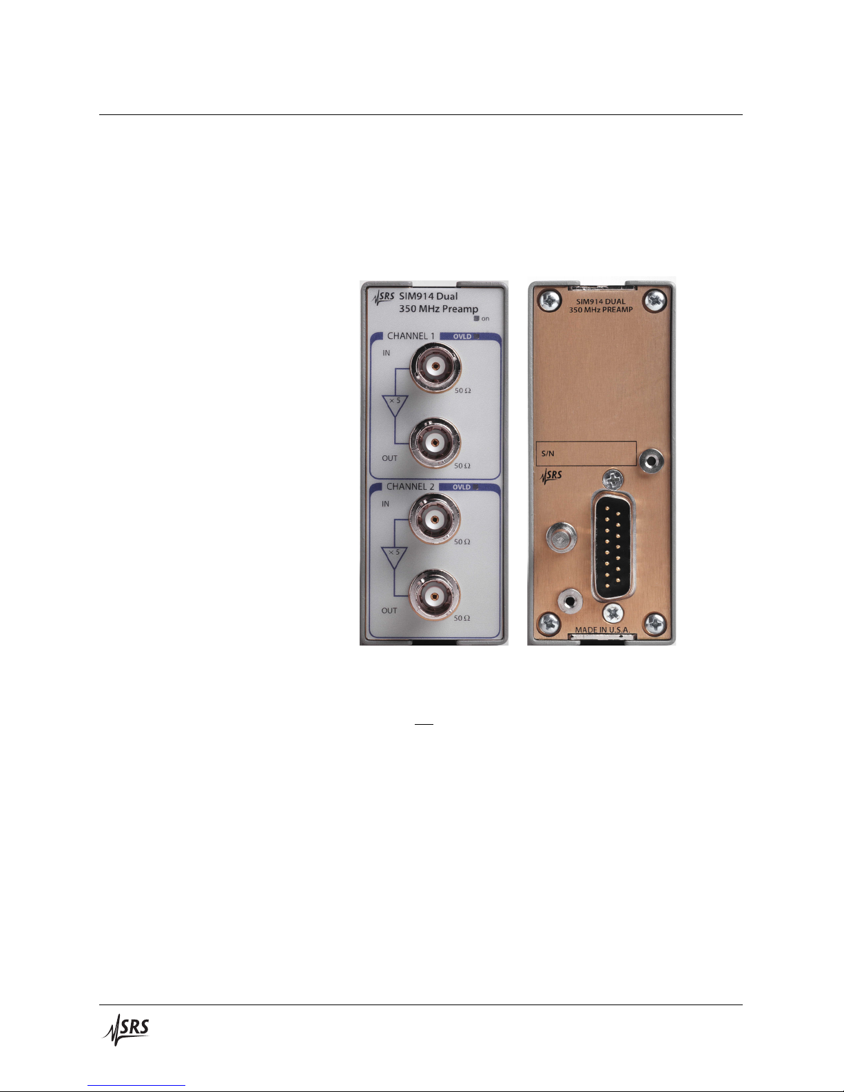
1.1 Description
The SIM914 is a two-channel, 350 MHz bandwidth, DC-coupled,
50 Ω amplifier with a gain of 5× (+14 dB). The two channels may be
cascaded for a gain of 25× (+28dB). The unit uses BNC connectors
for inputs and outputs (see Figure 1.1). A rear panel DB-15 connector
provides power to the unit.
Figure 1.1: The SIM914 front and rear panels.
The full scale input is ±200 mV. The input noise (above 1 kHz) is
typically 5.2 nV/
√
Hz. The output is linear over ±1 V and should be
terminated into a 50 Ω load. Output rise and fall times are 1.3 ns.
The output will recover from a 10× full-scale overload within 3 ns.
The unit is protected from ±50 V, 1 µs input overloads.
The SIM914 is powered by ±5 VDC from the SIM900 Mainframe.
There are three LEDs on the front panel. The green LED indicates
that power is present. The red LEDs indicate that the output signal
for the corresponding channel is outside its linear range, typically
±1.3 VDC. Brief overloads (<5 ns) trigger a 10 ms flash and will set
the overload status bit in the mainframe.
SIM914 350 MHz Preamplifier
Page 7

1.2 Operation 1 – 3
1.2 Operation
The SIM914 is typically installed in the SIM900 Mainframe, which
can accommodate up to eight SIM914s (plus one remote unit.) The
unit is on, as indicated by the front-panel Power LED, whenever the
mainframe has line power and is turned on.
The input impedance for each channel is 50 Ω. The DC input voltage must be limited to ±4 V to avoid damaging the amplifier frontend. The amplifier is internally protected from 50 V transients of 1 µs
duration. The 50 Ω input impedance is intended to terminate 50 Ω
coaxial cable such as RG-58.
The amplifiers perform well when cascaded due to their high input
return loss and flat frequency response characteristics. Referenced to
the input, the broadband noise (1 Hz to 300 MHz) is 80 µVrms. Peakto-peak noise is typically 5 times the rms value. This corresponds to
about 10 mVpp at the output of two cascaded amplifiers, 50 mVpp at
the output of three cascaded amplifiers, and 250 mVpp at the output
of four cascaded amplifiers.
1.3 SIM Interface Connector
The DB-15 SIM Interface Connector provides power and overload
monitoring to the instrument. The connector signals are specified in
the table below.
Pin Name Description
1 SIGNAL GND Ground
2 −STATUS Overload (TTL output, active low)
6 −5V Power supply
8 PS RTN Ground
9 CHASSIS GND Chassis ground
13 +5V Power supply
Table 1.1: SIM Interface Connector pin assignments, DB-15. All other
pins are left unconnected on the SIM914.
1.3.1 Grounding
In the SIM914, all three ground lines (Pins 1, 8 & 9) are tied common
to the chassis, and also form the signal ground.
SIM914 350 MHz Preamplifier
Page 8

1 – 4 Operation
1.3.2 Direct Interfacing
The primary connection to the SIM914˜Amplifier is the rear-panel
DB–15 SIM interface connector. Typically, the SIM914 is mated to
a SIM900 Mainframe via this connection, either through one of the
internal Mainframe slots, or the remote cable interface.
It is also possible to operate the SIM914 directly, without using the
SIM900 Mainframe. This section provides details on the interface.
CAUTION
The SIM914 has no internal protection against reverse polarity, missing
supply, or overvoltage on the power supply pins. Misapplication of power
may cause circuit damage. SRS recommends using the SIM914 together
with the SIM900 Mainframe for most applications.
The mating connector needed is a standard DB-15 receptacle, such
as Amp part # 747909-2 (or equivalent). Clean, well-regulated supply voltages of ±5 VDC must be provided, with +5 V supplied on
Pin 13 and −5 V supplied on Pin 6 (see Table 1.1). Ground may be
provided on any combination of Pins 1, 8 or 9. The −STATUS signal
may be monitored on Pin 2 for a low-going TTL-compatible output
indicating an amplifier overload condition.
SIM914 350 MHz Preamplifier
Page 9

1.4 Specifications 1 – 5
1.4 Specifications
Min Typ Max Units
Inputs (50 Ω source) Input signal level −200 +200 mV
Impedance 49.5 50 50.5 Ω
Return loss 32 dB
Offset −500 +500 µV
Offset drift −10 +10 µV/◦C
Bias current (note 1) 3 10 µA
Protection (DC) −4 +4 VDC
Protection (1µs transient) −50 +50 V
Recovery time (10× FS overload) 3 ns
Noise (10 Hz) 22 nV/
Noise (100 Hz) 8.6 nV/
Noise (>1 kHz) 5.2 nV/
Noise (1 Hz to 300 MHz BW) 80 µVrms
Crosstalk (CH1 out to CH2 in) −61 dB
Crosstalk (CH2 out to CH1 in) −82 dB
√
√
√
Hz
Hz
Hz
Amplifier Gain (note 2) 4.95 5.00 5.05 V/V
Bandwidth (−3 dB) 350 MHz
Rise/fall time 1.3 ns
Propagation delay 2.7 ns
Outputs (into 50 Ω) Source impedance 49.5 50 50.5 Ω
Linear operation −1.0 +1.0 V
Overload level −1.3 +1.3 V
Limit level −1.6 +1.6 V
General Number of Channels 2
Operating temperature 0 40
Weight 1.4 lbs
Power ±5 VDC
Supply current 80 mA
Dimensions 1.5” W ×3.6” H × 7.0” D
Notes:
1. The input bias current flows out of the unit, creating a positive offset
of about 150 µV on the 50 Ω input termination. This offset will be
affected by the DC impedance of the source that is connected to the
input.
2. Amplifier gain is calibrated by applying a known current to the input
and measuring the voltage into a high impedance load. The gain
is adjusted so that a 1 mA source applied to the input produces a
500 mV voltage at the unloaded output.
◦
C
SIM914 350 MHz Preamplifier
Page 10

1 – 6 Operation
SIM914 350 MHz Preamplifier
Page 11

2 Calibration
In This Chapter
This chapter describes how to adjust the SIM914 for optimum performance. The module should be warmed up for at least 15 minutes
before making any adjustments.
2.1 General . . . . . . . . . . . . . . . . . . . . . . . . . . 2 – 2
2.2 Required Equipment . . . . . . . . . . . . . . . . . . 2 – 2
2.3 High Frequency Compensation . . . . . . . . . . . 2 – 2
2.4 Offset Calibration . . . . . . . . . . . . . . . . . . . 2 – 3
2.5 Gain Calibration . . . . . . . . . . . . . . . . . . . . 2 – 3
2 – 1
Page 12

2 – 2 Calibration
2.1 General
The purpose of calibration is to verify operation of the unit and to:
• Adjust the high frequency compensation for best pulse response.
• Adjust the offset to null the DC voltage at the output with no
input.
• Adjust the gain to 10× for an unloaded output so that the
nominal gain for an amplifier driving a 50 Ω load will be 5×
(+14dB).
Since the adjustments are interdependent, it is important that the
adjustments be done in the prescribed order, and that all of the adjustments be done. For example, adjusting the high frequency compensation will affect the output offset.
2.2 Required Equipment
1. Pulse generator, splitter and attenuator to produce ±100 mV
square waves with a rise time of less than 1ns. (DG535 Digital
Delay/Pulse Generator, AB output, into unmatched tee driving two 50 Ω cables with a 20 dB attenuator on the one that
goes to the SIM914.)
2. Digital multimeter with 4-wire ohm measurement capability
(Agilent 34401).
3. Oscilloscope with at least 300 MHz bandwidth.
2.3 High Frequency Compensation
The SIM914 uses an AD8009 current feedback amplifier in the output stage. The gain of the amplifier is controlled by the ratio of resistors in the feedback network and the bandwidth is controlled by
the Thevenin equivalent source impedance of the feedback network.
The ratio is fixed (by R115 & R116 or R215 & R216) to provide a
gain of 5× and the source impedance may be adjusted (by P102 and
P202).
The bandwidth is set to optimize the pulse response of the amplifier.
This is done by applying a fast pulse at the input and adjusting P102
(or P202 for Channel 2) so that the output rise time and overshoot
most closely match the rise time and overshoot of the fast input pulse
as observed on a 300 MHz oscilloscope with 50 Ω input impedance.
Note that adjusting P102 will affect the offset for Channel 1, as there
is a large input bias current (150 µA max) to the inverting input of
SIM914 350 MHz Preamplifier
Page 13

2.4 Offset Calibration 2 – 3
the AD8009. The offset will need to be adjusted after the HF compensation is adjusted.
1. Split the pulse output from from the DG535 (set to 1 V amplitude) with a coax tee. Take one cable from the tee to channel 1
of the oscilloscope (set to 50 Ω input termination) and the other
to the top channel of the SIM914 via a 20 dB coaxial attenuator.
2. Adjust P102 (Channel 1 “HF COMP” pot) to match the output
rise time and overshoot to the input rise time and overshoot.
3. Repeat for Channel 2, adjusting the pulse response with P202.
2.4 Offset Calibration
The output offset is affected by the HF compensation and so the offset should be nulled after the HF compensation is adjusted. The
offset may also be affected by the amplifier gain adjustment if there
is a large input offset voltage.
1. Leave the inputs unconnected.
2.5 Gain Calibration
2. Connect the output (without a 50 Ω load) to the DMM on the
millivolt DC range.
3. Adjust P101 (Channel 1 “OFFSET” pot) to null the output voltage.
4. Verify that the output voltage shifts down by less than 2.5 mV
when a 50 Ω terminator is placed on the input. (The voltage
shift ∆V
= 10 × ib× ∆Rs, where ibis the input bias current,
out
and ∆Rsis the change in input source impedance, here 25 Ω.
This confirms that the input bias current ib< 10 µA.)
5. Repeat the procedure to null the output of Channel 2 by adjusting P201.
The overall gain of the amplifier is 5× when driving a 50 Ω load
and 10× when driving a high impedance load. The input source to
the amplifier is typically a current source (such as the output from a
photomultiplier tube) and so the magnitude of the input resistance is
included in the gain calibration by measureing the transimpedance.
(Calibration is done with a current source as an input while measuring the voltage at the output.)
SIM914 350 MHz Preamplifier
A DMM used in the 4-wire resistance mode is convenient for performing the calibration. Typically a DMM will measure small resistances by measuring the voltage across the resistor while passing a
Page 14

2 – 4 Calibration
1 mA DC current through the resistor. We measure the gain of the
amplifier by measuring the voltage at the output while applying test
current to input. When the gain is properly adjusted, 1 mA applied
to the 50 Ω input generates 50 mV at the input and 500 mV at the
(unterminated) output causing the DMM to indicate a “resistance”
of 500 Ω. (To avoid auto ranging confusion by the DMM, a 453 Ω
resistor is placed in series with the current source.)
Since the DMM uses a DC current as the test source, it is important
that the amplifier offset be nulled prior to performing the DC gain
adjustment.
1. Setup the DMM in the 4-wire resistance measurement mode.
2. Apply the current output to the Channel 1 input via a 453 Ω
in-line resistor.
3. Apply the unterminated Channel 1 output to the DMMs 4-wire
sense input.
4. Adjust P100 (Channel 1 “GAIN” pot) so that the DMM indicates a “resistance” of 500 Ω.
5. Verify that the offset was nulled by connecting the current
source from the DMM to the input of the other channel and
measuring a resistance of less than 1 Ω.
6. Repeat the gain adjustment for Channel 2 by adjusting P200.
SIM914 350 MHz Preamplifier
Page 15

3 Circuit Description
In This Chapter
This chapter gives a general discussion of the circuitry in the SIM914.
The two amplifier channels are identical. This description uses reference designators in the top channel, Channel 1.
3.1 Input Stage . . . . . . . . . . . . . . . . . . . . . . . 3 – 2
3.2 Output Stage . . . . . . . . . . . . . . . . . . . . . . 3 – 2
3.3 Overload Detection . . . . . . . . . . . . . . . . . . 3 – 2
3.4 Power . . . . . . . . . . . . . . . . . . . . . . . . . . . 3 – 3
3.5 Parts List . . . . . . . . . . . . . . . . . . . . . . . . . 3 – 4
3.6 Schematic Diagrams . . . . . . . . . . . . . . . . . . 3 – 5
3 – 1
Page 16

3 – 2 Circuit Description
3.1 Input Stage
The input is terminated into 50 Ω by the parallel combination of R100
& R101. The input signal is coupled via a 47 Ω resistor to the high
speed “clamp-amp,” U100. U100 is configured as a non-inverting
gain 2× amplifier. Pins 8 & 5 on U100 define input clamping thresholds of ±0.31 V. If the input signal exceeds these thresholds then
U100 will use the clamping thresholds as inputs, thereby limiting
the output to ±0.62 V. This prevents the output of U100 from overdriving the next gain stage.
Input signals in excess of ±1.4 V are shunted to ground via the input
protection diodes D100 & D101. Normally both the diodes in D100
are reversed biased and so they do not interfere with the signal. The
diodes in D101 are forward biased by R103 & R104. When the input
signal exceeds ±1.4 V (7× the full scale input), one of the diodes in
D100 will begin to conduct, thereby limiting the input to U100 to a
safe level.
The gain of U100 can be adjusted by ±10 % by P100, which is calibrated at the factory to set the overall gain of the channel to 5×when
terminated into a 50 Ω load. The output of U100 is passed to the next
gain stage via R112, a 47 Ω resistor.
3.2 Output Stage
3.3 Overload Detection
The next stage has a fixed gain of 5× with an adjustable offset and
adjustable high frequency response. The gain of U101 is set by R115
& R116. The offset, adjusted by P101 and injected by R117, is nulled
at the factory. The high frequency response of U101 is affected by
the source impedance of its input signal and its feedback network.
Turning P102 clockwise decreases the source impedance of the feedback signal and increases the high frequency response of the gain
stage. P102 is adjusted at the factory for an optimum pulse response
providing a typical −3dB bandwidth of 350 MHz.
The output from U101 is passed to the front-panel output BNC
via the parallel resistors R118 & R119, providing a 50 Ω output
impedance. These resistors, in combination with the 50 Ω load resistor (provided by the user), attenuate the signal by 2× so that the
overall gain is 5×.
Overloads are detected at the output of the second gain stage, U101.
A positive overload is rectified by D102 and charges C107. A negative overload is rectified by D102 and discharges C106. One of the
SIM914 350 MHz Preamplifier
Page 17

3.4 Power 3 – 3
comparators in U102 will be driven low when the voltage on C106 or
C107 exceeds ±1.7 V. The driven comparator discharges C108 from
+5 V to −5 V. C108 will be slowly recharged to +5 V by R128, a
1 MΩ resistor, thereby stretching the overload signal to about 10 ms.
One of the comparators in U300 drives the front-panel overload LED
until the voltage on C108 recharges above ground. This overload detection will detect overloads as short as 3 ns.
The overload detectors are wire-ord by D303 which will pull the status pin (pin 2 on the rear-panel connector to the SIM mainframe) to
0 V via the 3.9 V Zener diode when an overload occurs. The status
pin may be polled via the SIM900 Mainframe to detect overloads in
the unit.
3.4 Power
The ±5 VDC power supplies are filtered at the rear panel (by L1, L3,
C1 & C2), again on the main PCB (by L2, L4, C300 & C301), and finally at each channel of the amplifier (L100, L101, C110 & C111 for
the top channel and L200, L201, C210 & C211 for the bottom channel.) Careful power supply filtering is important to reduce channel
crosstalk. The crosstalk from the output of Channel 1 to the input
of Channel 2 is less than −60dB (1:1000 of the amplitude) and peaks
around 300 MHz. The crosstalk from the output of Channel 2 to the
input of Channel 1 is less than −80dB (1:10,000 of the amplitude) and
occurs in a broad band between 180 MHz and 360 MHz.
SIM914 350 MHz Preamplifier
Page 18

3 – 4 Circuit Description
Qnt Reference SRS P/N Part Qnt Reference SRS P/N Part
8 C1,C2,C110,C111,C210, 5-00472 4.7U-35T 2 J303,J304 mounting 0-00259 4-40X1/2PP
C211,C300,C301 3 J305,J306,J307 mounting 0-00241 4-40X3/16 PP
5 C3,C106,C107,C206,C207 5-00375 100P 2 J303,J304 mounting 0-00042 4-40 HEX
12 C100,C101,C102,C103,C104, 5-00299 .1U 2 J303,J304 mounting 0-00043 4-40 KEP
C105,C200,C201,C202,C203, 2 DB-15 mounting 0-00835 4-40X3/8PF
C204,C205 4 Front panel mounting 0-00148 4-40X1/8,PS
2 C108,C208 5-00298 .01U 4 Rear panel mounting 0-00515 4-40X1/8PP
1 D1 3-01429 MMBZ5228B 8 Module Cover Mounting 0-00371 4-40X3/16P
6 D100,D101,D102,D200,D201, 3-00896 BAV99L 1 Front Panel, SIM914 7-00987
D202 1 Lexan FP Overlay, SIM914 7-01353
1 D300 3-00424 LED-G 1 Rear Panel, SIM914 7-01410
2 D301,D302 3-00425 LED-R 2 SIM 1X BRACKET 7-00933
1 D303 3-00649 MBAW56L 2 SIM Module Cover 7-00932
1 J1 1-00367 DB15-GND 4 Foot 0-00188 SR550FOOT
4 J100,J101,J200,J201 1-00003 BNC
1 J311 TO J312 1-00483 Jumper 4X1 (2")
1 J2-J5 1-01042 Jumper 4X1 (4")
8 L1,L2,L3,L4,L100,L101, 6-00236 BEAD
L200,L201
2 P100,P200 4-00487 20
2 P101,P201 4-00011 10K-10T
4 R103,R104,R203,R204 4-01503 10K
2 P102,P202 4-00353 100-10T
9 R1,R105,R107,R121,R125 4-01455 100
R205,R207,R221,R225
4 R2,R300,R307,R308 4-01479 1K
12 R100,R101,R109,R110,R118, 4-01021 100/1%
R119,R200,R201,R209,R210,
R218,R219
4 R102,R112,R202,R212 4-01447 47
8 R106,R108,R122,R123,R206, 4-01134 1.50K
R208,R222,R223
2 R115,R215 4-01050 200/1%
2 R116,R216 4-01280 49.9
2 R117,R217 4-01213 10.0K
4 R120,R124,R220,R224 4-01527 100K
4 R126,R127,R226,R227 4-01163 3.01K
2 R128,R228 4-01551 1M
2 U100,U200 3-00897 AD8037
2 U101,U201 3-00898 AD8009
3 U102,U202,U300 3-00728 LM393
1 PCB 7-00967 SIM914 Rev C
3.5 Parts List
SIM914 350 MHz Preamplifier
Page 19

3.6 Schematic Diagrams 3 – 5
3.6 Schematic Diagrams
Schematic diagrams follow this page.
SIM914 350 MHz Preamplifier
 Loading...