

Page 1

Operation and Service Manual
Stanford Research Systems
JFET Preamp
SIM910
Revision 2.1 • May 8, 2007
Page 2

Certification
Stanford Research Systems certifies that this product met its published specifications at the time
of shipment.
Warranty
This Stanford Research Systems product is warranted against defects in materials and workmanship for a period of one (1) year from the date of shipment.
Service
For warranty service or repair, this product must be returned to a Stanford Research Systems
authorized service facility. Contact Stanford Research Systems or an authorized representative
before returning this product for repair.
Information in this document is subject to change without notice.
Copyrightc Stanford Research Systems, Inc., 2003 – 2007. All rights reserved.
Stanford Research Systems, Inc.
1290–D Reamwood Avenue
Sunnyvale, CA 94089 USA
Phone: (408) 744-9040 • Fax: (408) 744-9049
www.thinkSRS.com • e-mail: info@thinkSRS.com
Printed in U.S.A. Document number 9-01553-903
SIM910 JFET Preamp
Page 3

Contents
General Information iii
Safety and Preparation for Use . . . . . . . . . . . . . . . . iii
Symbols . . . . . . . . . . . . . . . . . . . . . . . . . . . . . iv
Notation . . . . . . . . . . . . . . . . . . . . . . . . . . . . . v
Specifications . . . . . . . . . . . . . . . . . . . . . . . . . . vi
1 Operation 1 – 1
1.1 Instrument Overview . . . . . . . . . . . . . . . . . . . 1– 2
1.2 Front Panel Operation . . . . . . . . . . . . . . . . . . 1 – 2
1.3 Rear Panel Output . . . . . . . . . . . . . . . . . . . . 1 –5
1.4 SIM Interface . . . . . . . . . . . . . . . . . . . . . . . . 1 – 6
2 Remote Operation 2 – 1
2.1 Index of Common Commands . . . . . . . . . . . . . . 2 – 2
2.2 Alphabetic List of Commands . . . . . . . . . . . . . . 2– 3
2.3 Introduction . . . . . . . . . . . . . . . . . . . . . . . . 2– 4
2.4 Commands . . . . . . . . . . . . . . . . . . . . . . . . . 2 – 5
2.5 Register Model . . . . . . . . . . . . . . . . . . . . . . 2 – 9
3 Performance Tests 3 – 1
3.1 Offset . . . . . . . . . . . . . . . . . . . . . . . . . . . . 3 – 2
3.2 Calibration . . . . . . . . . . . . . . . . . . . . . . . . . 3 – 2
3.3 Performance Tests . . . . . . . . . . . . . . . . . . . . . 3 – 3
3.4 SIM910 Performance Test Record . . . . . . . . . . . . 3 – 4
4 Circuitry 4 – 1
4.1 Circuit Discussion . . . . . . . . . . . . . . . . . . . . . 4 – 2
4.2 Parts List . . . . . . . . . . . . . . . . . . . . . . . . . . 4– 4
4.3 Schematic Diagrams . . . . . . . . . . . . . . . . . . . 4 – 4
i
Page 4

ii Contents
SIM910 JFET Preamp
Page 5

General Information
The SIM910 JFET Preamp, part of Stanford Research Systems’ Small
Instrumentation Modules family, is a low noise general purpose voltage preamplifier with bandwidth from DC to 1 MHz.
Safety and Preparation for Use
Biomedical Applications
Under certain conditions, the SIM910 may prove to be unsafe for
WARNING
Regarding Use with Photomultipliers
CAUTION
applications involving human subjects. Incorrect grounding, component failure, and excessive common-mode input voltages are examples of conditions in which the instrument may expose the subject
to large input currents. Therefore, Stanford Research Systems does
not recommend the SIM910 for such applications.
The front-end amplifier of this instrument is easily damaged if a
photomultiplier is used improperly with the amplifier. When left
completely unterminated, a cable connected to a PMT can charge
to several hundred volts in a relatively short time. If this cable is
connected to the inputs of the SIM910, the stored charge may damage
the front-end JFETs. To avoid this problem, provide a leakage path of
about 100 kΩ to ground inside the base of the PMT to prevent charge
accumulation.
Service
Do not install substitute parts or perform any unauthorized modifications to this instrument.
The SIM910 is a single-wide module designed to be used inside the
SIM900 Mainframe. Do not turn on the power until the module is
completely inserted into the mainframe and locked in place.
iii
Page 6
iv General Information
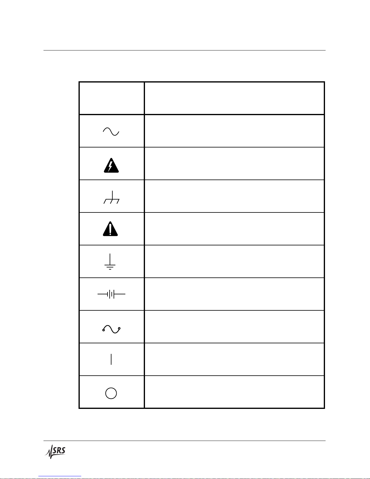
Symbol Description
Alternating current
Caution - risk of electric shock
Frame or chassis terminal
Caution - refer to accompanying documents
Earth (ground) terminal
Battery
Fuse
On (supply)
Off (supply)
Symbols you may Find on SRS Products
SIM910 JFET Preamp
Page 7

General Information v
Notation
The following notation will be used throughout this manual:
WARNING
CAUTION
A warning means that injury or death is possible if the instructions
are not obeyed.
A caution means that damage to the instrument or other equipment
is possible.
• Front-panel buttons are set as [Button];
[Adjust ] is shorthand for “[Adjust ] & [Adjust ]”.
• Front-panel indicators are set as OVLD.
• Remote command names are set as *IDN?.
• Literal text other than command names is set as OFF.
SIM910 JFET Preamp
Page 8

vi General Information
Specifications
Performance Characteristics
Frequency range DC to 1 MHz; −3 dB @ 1.9 MHz, typ.
Gain 1, 2, 5, 10, 20, 50, 100
Gain accuracy ±0.5 % DC to 100 kHz
± 5 % @ 1 MHz, typ.
Gain stability 200 ppm/◦C
Input voltage noise (RTI, gain ≥ 10) 4 nV/√Hz@ 1 kHz, typ.
gain 1 12nV/√Hz@ 1 kHz, typ.
Input current noise <10 fA/√Hz, typ.
Input impedance 100MΩ // 35 pF
Input Bias Current (DC) 0.5 pA, typ.
Output impedance 50Ω
AC coupling frequency 16 mHz −3dB
Input selection A, A−B, GND
Input coupling AC or DC
Input shields Floating or ground
Maximum input, differential ±1 V before overload
Maximum input, common-mode ±5 V
clamped at ±6 V
Maximum output voltage ±10 V before overload
Maximum output current ±100 mA before overload
Maximum slew rate 0.4 V/µs RTI, typ.
2.4 V/µs RTO, typ.
CMRR 85 dB @ 1 kHz
Offset stability ±10 ppm/◦C max
General Characteristics
Operating temperature 0◦C to 40◦C, non-condensing
Power +5 V (50 mA typ., 100 mA max.)
±15 V (50 mA typ., 300 mA max.)
Interface Serial (RS-232) through SIM interface
Connectors BNC (3 front, 1 rear)
DB–15 (male) SIM interface
Weight 1.5 lbs
Dimensions 1.500W × 3.600H × 7.000D
SIM910 JFET Preamp
Page 9

1 Operation
In This Chapter
The SIM910 JFET Preamp is a flexible low noise voltage preamplifier
for general use from DC to 1 MHz. This chapter gives the necessary
information to get started quickly with the SIM910.
1.1 Instrument Overview . . . . . . . . . . . . . . . . . . 1 – 2
1.2 Front Panel Operation . . . . . . . . . . . . . . . . . . 1– 2
1.2.1 Gain . . . . . . . . . . . . . . . . . . . . . . . . 1 – 3
1.2.2 Offset . . . . . . . . . . . . . . . . . . . . . . . . 1 – 3
1.2.3 Overload . . . . . . . . . . . . . . . . . . . . . . 1– 3
1.2.4 Inputs . . . . . . . . . . . . . . . . . . . . . . . 1 – 4
1.2.5 Output . . . . . . . . . . . . . . . . . . . . . . . 1 – 4
1.3 Rear Panel Output . . . . . . . . . . . . . . . . . . . . 1 – 5
1.4 SIM Interface . . . . . . . . . . . . . . . . . . . . . . . 1 – 6
1.4.1 SIM interface connector . . . . . . . . . . . . . 1 – 6
1.4.2 Direct interfacing . . . . . . . . . . . . . . . . . 1 – 6
1 – 1
Page 10
1 – 2 Operation
A
B
INPUT
A / A-B
AC /
DC
SHIELD
FLOAT/GND
INPUT
GROUND
+
-
FRONT
END
PROGRAMMABLE
GAIN
Ω
50
OUTPUT
REAR
PANEL
OUT
INPUT
PROTECTION
1.1 Instrument Overview
The SIM910 is a voltage preamplifier with low input and output
noise. It provides selectable gain from 1 to 100 of a single ended or
true differential signal. The amplifier runs from DC to 1 MHz, or can
be AC coupled with 16 mHz −3dB frequency. In addition, the input
BNC shields can be grounded or floated allowing the signal ground
to be referenced to a local or remote ground. An overload light
indicates when the input or output maximum voltage, or maximum
output current has been reached.
The amplifier settings can be controlled either by the front panel
buttons or the remote serial interface. Digital noise is eliminated by
only clocking the microprocessor when settings are being changed.
The complete amplifier configuration (i.e., gain settings, coupling,
etc.) is saved in non-volatile memory.
The front end amplifier of this instrument is protected with a pair of
100 Ω resistors (R103 & R104). Note that the internal-grounding input configuration grounds the amplifier inputs after these protection
resistors.
1.2 Front Panel Operation
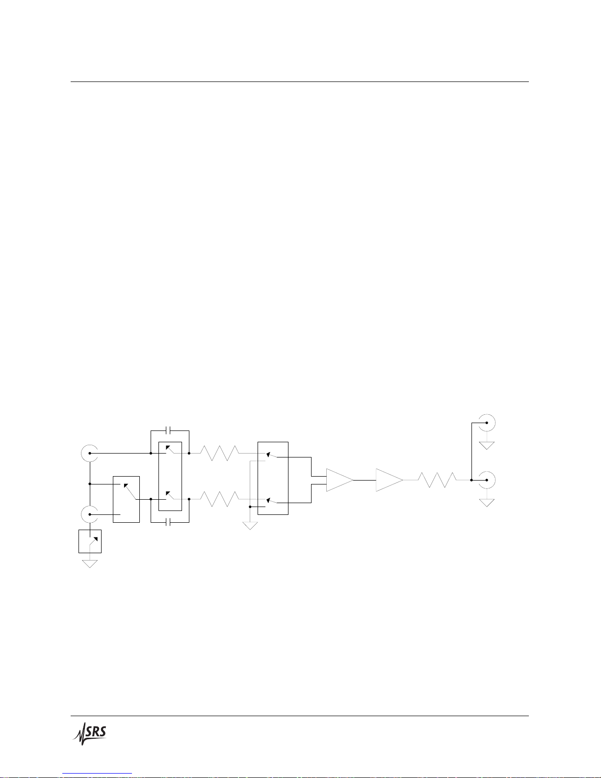
A block diagram of the amplifier is shown below in Figure 1.1.
Figure 1.1: The SIM910 block diagram.
All SIM910 configurations can be specified either from the front
panel, or by commanding through the remote serial interface. The
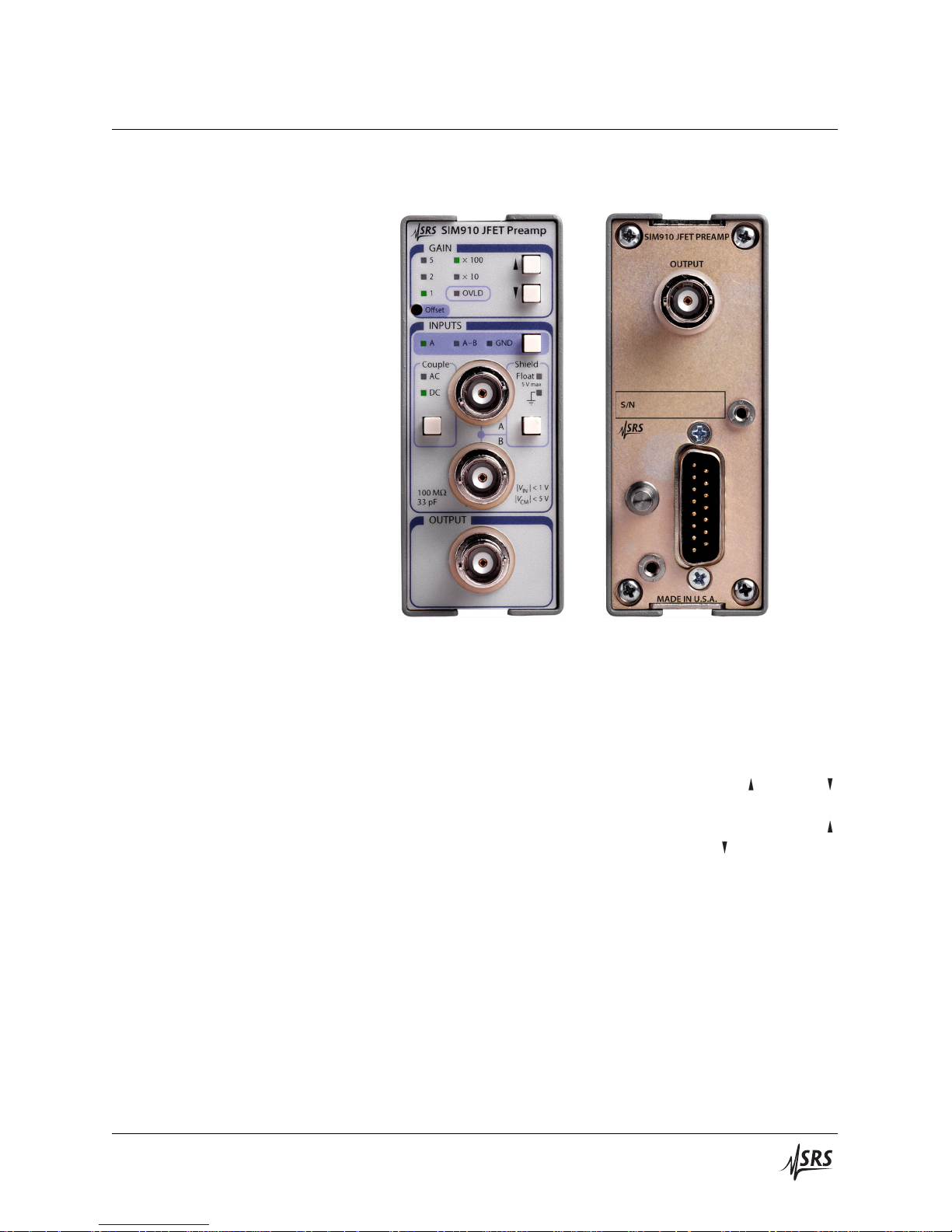
front panel is shown below (Figure 1.2). The front panel contains the
SIM910 JFET Preamp
Page 11
1.2 Front Panel Operation 1 – 3
gain settings, the overload light, the input settings, the coupling and
the shield states, and the buttons to control them.
1.2.1 Gain
1.2.2 Offset
1.2.3 Overload
Figure 1.2: The SIM910 front and rear panel.
The gain is selectable from 1 to 100. Gain settings are 1, 2, 5, 10, 20, 50,
and 100 and are displayed as a product of 1, 2, or 5 and a multiplier
of 10 or 100. Gain is raised or lowered by pressing [Gain ] or [Gain ]
in the GAIN block on the upper right of the module. The change
is reflected in the LEDs to the left of the buttons. Pushing [Gain ]
when on gain 100 produces no effect. Pushing [Gain ] when on gain
1 produces no effect.
The offset is adjustable through a hole in the GAIN block of the
front panel with a small flat head screwdriver. See Section 3.1 for a
description of the offset trimming procedure.
There is an overload light in the gain section of the front panel. OVLD
is lit when the input common mode is outside ±5 V, the input signal is
SIM910 JFET Preamp
Page 12

1 – 4 Operation
greater than ±1 V, or the output is outside ±10 V. The overload signal
can also be asserted on the status pin. See section 2.4.5.
1.2.4 Inputs
The two input connectors, labeled A and B, are in the INPUT block
of the front panel. [Input] selects between A, A−B, and Ground. A
& B are voltage inputs with input impedance of 100 MΩ in parallel
with ∼35 pF. The connector shields are tied to each other, and can be
either floated or grounded to Signal Ground using [Shield]. Input
A is the non-inverting input. When input A−B is selected, B is the
inverting input.
When input A is selected, the connector shield is used as the inverting
input, and acts as the reference for the A signal. Thus by selecting
Shield Float, a remote ground reference can be brought to the unit
using a single BNC. As long as the common-mode voltage limit is
satisfied, this configuration can be useful in breaking ground loops.
If the common-mode limits are exceeded, the inputs will be (sepa-overload limits
rately) clamped to ∼ ±6 V through a series input resistor of 100 Ω.
The maximum signal voltage is ±1 V, while the maximum common
mode voltage is ±5V. Exceeding these limits will cause OVLD to
light up.
1.2.5 Output
When the Ground input is selected, the user inputs A & B are left
floating and the amplifier is internally grounded at the front-end,
after the series resistors. The Input grounded noise is the limit of the
amplifier’s noise.
Pressing [Couple] selects AC (16 mHz −3dB) or DC coupling.
The output of the instrument is located in the OUTPUT block of the
front panel. The output is referred to Signal Ground, which is tied to
the outside of the BNC connector.
The chassis of the SIM910 is tied to the power supply return, and notNote about grounds
Signal Ground. When operating in the SIM900, the chassis and Signal
Ground are tied together in the SIM900 Mainframe. If the amplifier is
operated with an independent supply, the output will be referenced
to Signal Ground (pin 1 on DB–15 J401). The Signal Ground and the
chassis are tied through back to back protection schottky diodes, so
they can’t be more than ∼ ±0.35 V apart.
The instrument’s output impedance is 50 Ω, and can drive load
impedances from ∞ down to 50 Ω. Note: when driving a 50 Ω load
the gain will be half that displayed on the LEDs.
SIM910 JFET Preamp
Page 13

1.3 Rear Panel Output 1 – 5
1.3 Rear Panel Output
The rear panel contains a BNC connected to the output, and the SIM
interface connector (see Figure 1.2).
The rear panel output is wired in parallel to the front panel output.
The output is not designed to drive 2 simultaneous 50Ω loads. If
one output is driving a 50 Ω load, the other should be connected to a
high impedance load.
SIM910 JFET Preamp
Page 14

1 – 6 Operation
1.4 SIM Interface
The primary connection to the SIM910 JFET Preamp is the rear-panel
DB–15 SIM interface connector. Typically, the SIM910 is mated to
a SIM900 Mainframe via this connection, either through one of the
internal mainframe slots, or the remote cable interface.
It is also possible to operate the SIM910 directly, without using the
SIM900 Mainframe. This section provides details on the interface.
CAUTION
The SIM910 has no internal protection against reverse polarity, missing
supply, or overvoltage on the power supply pins. Misapplication of power
may cause circuit damage. SRS recommends using the SIM910 together
with the SIM900 Mainframe for most applications.
1.4.1 SIM interface connector
The DB–15 SIM interface connector carries all the power and communications lines to the instrument. The connector signals are specified
in Table 1.1
Pin Signal Src ⇒ Dest Description
1 SIGNAL GND MF ⇒ SIM Ground reference for signal
2 −STATUS SIM ⇒ MF Status/service request (GND = asserted, +5 V= idle)
3 RTS MF ⇒ SIM HW Handshake (+5 V= talk; GND = stop)
4 CTS SIM ⇒ MF HW Handshake (+5 V= talk; GND = stop)
5 −REF 10MHZ MF ⇒ SIM 10 MHz reference (no connection in SIM910)
6 −5 V MF ⇒ SIM Power supply (no connection in SIM910)
7 −15 V MF ⇒ SIM Power supply (analog circuitry)
8 PS RTN MF ⇒ SIM Power supply return
9 CHASSIS GND Chassis ground
10 TXD MF ⇒ SIM Async data (start bit = “0”= +5 V; “1” = GND)
11 RXD SIM ⇒ MF Async data (start bit = “0”= +5 V; “1” = GND)
12 +REF 10MHz MF ⇒ SIM 10 MHz reference (no connection in SIM910)
13 +5 V MF ⇒ SIM Power supply (digital circuitry)
14
+15 V MF ⇒ SIM Power supply (analog circuitry)
15 +24 V MF ⇒ SIM Power supply (no connection in SIM910)
Direction
1.4.2 Direct interfacing
Table 1.1: SIM Interface Connector Pin Assignments, DB-15
The SIM910 is intended for operation in the SIM900 Mainframe, but
users may wish to directly interface the module to their own systems
without the use of additional hardware.
SIM910 JFET Preamp
Page 15

1.4 SIM Interface 1 – 7
The mating connector needed is a standard DB–15 receptacle, such as
Amp part # 747909-2 (or equivalent). Clean, well-regulated supply
voltages of +5, ±15 VDC must be provided, following the pin-out
specified in Table 1.1. Ground must be provided on pins 1 and 8,
with chassis ground on pin 9. The −STATUS signal may be monitored
on pin 2 for a low-going TTL-compatible output indicating a status
message.
1.4.2.1 Direct interface cabling
If the user intends to directly wire the SIM910 independent of the
SIM900 Mainframe, communication is usually possible by directly
connecting the appropriate interface lines from the SIM910 DB–15
plug to the RS-232 serial port of a personal computer.1Connect RXD
from the SIM910 directly to RD on the PC, TXD directly to TD, and
similarly RTS→RTS and CTS→CTS. In other words, a null-modem
style cable is not needed.
To interface directly to the DB–9 male (DTE) RS-232 port typically
found on contemporary personal computers, a cable must be made
with a female DB–15 socket to mate with the SIM910, and a female
DB–9 socket to mate with the PC’s serial port. Separate leads from
the DB–15 need to go to the power supply, making what is sometimes
know as a “hydra” cable. The pin-connections are given in Table 1.2.
DB–15/F to SIM910 Name
DB–9/F
3 ←→7 RTS
4 ←→8 CTS
10 ←→3 TxD
11 ←→2 RxD
5 Computer Ground
to P/S
7 ←→ −15 VDC
14 ←→ +15 VDC
13 ←→ +5 VDC
8,9 ←→ Ground (P/S return current)
1 ←→ Signal Ground (separate wire to Ground)
Table 1.2: SIM910 Direct Interface Cable Pin Assignments
1
Although the serial interface lines on the DB-15 do not satisfy the minimum
voltage levels of the RS-232 standard, they are typically compatible with desktop
personal computers
SIM910 JFET Preamp
Page 16

1 – 8 Operation
The Chassis Ground and Power Ground are tied together in the in-more about grounding
strument. The +5 V sections use the Power Ground, and the signal
sections of the instrument use the ±15 V and Signal Ground. The
Signal Ground and Power Ground are tied through protection schottky diodes, and can therefore not be more than ∼ ±0.35 V apart.
These two ground lines should be separately wired back to a single,
low-impedance ground source at the power supply.
1.4.2.2 Serial settings
The serial port settings at power-on are: 9600 baud, 8–bits, no parity,
1 stop bit, and hardware flow control (see Section 2.3.1). The serial
settings cannot be changed on the SIM910.
SIM910 JFET Preamp
Page 17

2 Remote Operation
In This Chapter
This chapter describes operating the module over the serial interface.
2.1 Index of Common Commands . . . . . . . . . . . . . 2 – 2
2.2 Alphabetic List of Commands . . . . . . . . . . . . . 2 – 3
2.3 Introduction . . . . . . . . . . . . . . . . . . . . . . . . 2– 4
2.3.1 Power-on configuration . . . . . . . . . . . . . 2– 4
2.3.2 Buffers . . . . . . . . . . . . . . . . . . . . . . . 2 – 4
2.3.3 Device Clear . . . . . . . . . . . . . . . . . . . . 2 – 4
2.4 Commands . . . . . . . . . . . . . . . . . . . . . . . . 2– 5
2.4.1 Command syntax . . . . . . . . . . . . . . . . . 2 – 5
2.4.2 Notation . . . . . . . . . . . . . . . . . . . . . . 2– 5
2.4.3 Examples . . . . . . . . . . . . . . . . . . . . . 2 – 5
2.4.4 Amplifier commands . . . . . . . . . . . . . . . 2 – 6
2.4.5 Status commands . . . . . . . . . . . . . . . . . 2 – 7
2.4.6 Interface commands . . . . . . . . . . . . . . . 2 – 8
2.5 Register Model . . . . . . . . . . . . . . . . . . . . . . 2– 9
2.5.1 Status Byte (SB) . . . . . . . . . . . . . . . . . . 2– 9
2.5.2 Service Request Enable (SRE) . . . . . . . . . . 2– 10
2 – 1
Page 18

2 – 2 Remote Operation
2.1 Index of Common Commands
symbol definition
i Integers
(?) Required for queries; illegal for set commands
{var} Required parameter for set commands; illegal for queries
Amplifier
*RST 2 – 6 Reset
GAIN(?) {i} 2 – 6 Gain
COUP(?) {i} 2 – 6 Coupling
INPT(?) {i} 2 – 6 Input
SHLD(?) {i} 2 – 6 Shield
Status
*STB? 2 – 7 Status Byte
*SRE(?) {i} 2 – 7 Service Request Enable
STOL(?) {i } 2 – 7 Status Monitors Overload
OVLD? 2 – 7 Overload
Interface
*IDN? 2 – 8 Identify
*TST? 2 – 8 Self Test
CONS(?) {i} 2 – 8 Console Mode
SIM910 JFET Preamp
Page 19

2.2 Alphabetic List of Commands 2 – 3
2.2 Alphabetic List of Commands
?
*IDN? 2 – 8 Identify
*RST 2 – 6 Reset
*SRE(?) {i} 2 – 7 Service Request Enable
*STB? 2 – 7 Status Byte
*TST? 2 – 8 Self Test
C
CONS(?) {i} 2 – 8 Console Mode
COUP(?) {i} 2 – 6 Coupling
G
GAIN(?) {i} 2 – 6 Gain
I
INPT(?) {i} 2 – 6 Input
O
OVLD? 2 – 7 Overload
S
SHLD(?) {i} 2 – 6 Shield
STOL(?) {i } 2 – 7 Status Monitors Overload
SIM910 JFET Preamp
Page 20

2 – 4 Remote Operation
2.3 Introduction
Remote operation of the SIM910 is through a simple command language documented in this chapter. Both set and query forms of most
commands are supported, allowing the user complete control of the
amplifier from a remote computer, either through the SIM900 Mainframe or directly via RS-232 (see Section 1.4.2.1).
See Table 1.1 for specification of the DB–15 SIM interface connector.
2.3.1 Power-on configuration
The settings for the remote interface are 9600 baud with no parity,
hardware flow control, and local echo disabled (CONS OFF).
Most of the SIM910 instrument settings are stored in non-volatile
memory, and at power-on the instrument returns to the state it was
last in when power was removed. Exceptions are noted in the command descriptions.
Reset values of parameters are shown in boldface.
2.3.2 Buffers
2.3.3 Device Clear
Incoming data from the host interface is stored in a 32-byte input
buffer. Characters accumulate in the input buffer until a command
terminator (either hCRi or hLFi) is received, at which point the message is parsed and executed. Query responses from the SIM910 are
buffered in a 64-byte output queue.
If the input buffer overflows, then all data in both the input buffer
and the output queue are discarded, and an error is recorded in the
CESR and ESR status registers.
The SIM910 host interface can be asynchronously reset to its poweron configuration by sending an RS-232-style hbreakisignal. From the
SIM900 Mainframe, this is accomplished with the SRST command;
if directly interfacing via RS-232, then use a serial break signal. After
receiving the Device Clear, the interface is reset to 9600 baud and
CONS mode is turned OFF. Note that this only resets the communi-
cation interface; the basic function of the SIM910 is left unchanged;
to reset the instrument, see *RST.
SIM910 JFET Preamp
Page 21

2.4 Commands 2 – 5
2.4 Commands
This section provides syntax and operational descriptions for remote
commands.
2.4.1 Command syntax
The four letter mnemonic (shown in CAPS) in each command sequence specifies the command. The rest of the sequence consists of
parameters.
Commands may take either set or query form, depending on whether
the “?” character follows the mnemonic. Set only commands are
listed without the “?”, query only commands show the “?” after the
mnemonic, and optionally query commands are marked with a “(?)”.
Parameters shown in { } are not always required. Parameters in { }
are required to set a value, and are omitted for queries. Parameters
listed without any surrounding characters are always required.
Do not send ( ) or { } as part of the command.
2.4.2 Notation
2.4.3 Examples
Multiple parameters are separated by commas. Commands are terminated by either hCRi or hLFi characters. Null commands and
whitespace are ignored. Execution of command(s) does not begin
until the command terminator is received.
The following table summarizes the notation used in the command
descriptions:
symbol definition
i Integers
(?) Required for queries; illegal for set commands
{var} required parameter for set commands; illegal for queries
Each command is provided with a simple example illustrating its
usage. In these examples, all data sent by the host computer to
the SIM910 are set as straight teletype font, while responses
received the host computer from the SIM910 are set as slanted
teletype font.
SIM910 JFET Preamp
Page 22

2 – 6 Remote Operation
2.4.4 Amplifier commands
These commands provide control over the settings of the amplifier
circuitry. All of these commands are persistent, in the sense that the
module will restore the last amplifier configuration upon power-on
reset.
Reset*RST
Reset the amplifier to default configuration.
In response to *RST, the amplifier settings become: unity gain, AC
coupling, input grounded, shield floated.
*RSTExample:
GainGAIN(?) {i}
Set (query) the amplifier gain {to i=(1, 2, 5, 10, 20, 50, 100)}.
GAIN?Example:
50
CouplingCOUP(?) {i}
Set (query) the amplifier input coupling.
COUP 1 sets AC coupling, while COUP 2 sets DC coupling.
COUP 1Example:
InputINPT(?) {i}
Set (query) the amplifier input.
INPT 1 sets the amplifier input to A, INPT 2 selects A−B, and INPT 3
grounds the amplifier front-end.
INPT 2Example:
ShieldSHLD(?) {i}
Set (query) the amplifier input BNC shield configuration.
SHLD 1 floats the A & B input shields, while SHLD 2 ties the input
shields to amplifier ground.
SHLD?Example:
1
SIM910 JFET Preamp
Page 23

2.4 Commands 2 – 7
2.4.5 Status commands
The Status commands query and configure registers associated with
status reporting of the SIM910.
Status Byte*STB?
Reads the Status Byte register.
Execution of the *STB? query clears all flag bits set in the Status Byte
register (see the Register Model section 2.5 for more about the Status
Byte register).
*STB also causes the −STATUS signal to be deasserted, as long as the
module is not in Status-Monitors-Overload mode (see STOL).
*STB?Example:
128
Service Request Enable*SRE(?) {i}
Set (query) the Service Request Enable register {to i} See section 2.5.
*SRE 128Example:
Status Monitors OverloadSTOL(?) {i }
Set (query) the Status-Monitors-Overload mode {to i=(0, 1)}.
STOL 1 causes the −STATUS signal (pin 2 on J401 Dsub-15 connec-
tor) to become a real-time monitor of the amplifier overload detect
circuit. STOL 0 restores −STATUS to reflect the overall service request message from the Status Byte register. In applications where
prompt flagging of an amplifier overload is required, STOL 1 mode
provides a single interface line for this signal.
The state of STOL is stored in non-volatile memory and restored
upon power-on reset. Neither *RST nor device-clear affects the state
of STOL.
STOL 0Example:
OverloadOVLD?
Reports the current overload condition. Query returns 0 for normal
operation, or 1 if the amplifier is presently in overload.
OVLD?Example:
1
SIM910 JFET Preamp
Page 24

2 – 8 Remote Operation
2.4.6 Interface commands
The interface commands provide information and control over the
communication link between the SIM910 and the host computer.
None of these commands have any effect on the amplifier function
itself.
Identify*IDN?
Query the device identification string.
The identification string is formatted as:
Stanford Research Systems,SIM910,S/N******,VER#.##
where ****** is the 6-digit serial number, and #.## is the firmware
revision level.
*IDN?Example:
Stanford Research Systems,SIM910,s/n003456,ver2.10
Self Test*TST?
Query the device self test.
The SIM910 does not perform any self tests, and will always return
the message 0 to this query.
*TST?Example:
0
Console ModeCONS(?) {i}
Set (query) the Console mode {to i=(0, 1)}.
CONS 1 causes each character received at the Input Buffer to be
echoed to the Output Queue. This mode can be useful when typing
interactively to the SIM910.
On device clear, CONS is set to 0 (off).
CONS?Example:
0
SIM910 JFET Preamp
Page 25

2.5 Register Model 2 – 9
2.5 Register Model
The SIM910 monitors and reports errors and other conditions using
a single 8-bit register, the Status Byte register. Each bit in the register
is mapped to a particular event category, and if that event occurs the
corresponding bit is set to 1. Bits in the Status Byte are “sticky,” in
the sense that once set to 1, the bit will not revert to the 0 (zero) value
even after the condition that caused the event has completed. Bits
are only cleared by querying the register.
A companion register, the Service Request Enable, acts as a bitwise
mask to the Status Byte for generating the −STATUS signal.
2.5.1 Status Byte (SB)
This is an 8-bit wide register. It can be read through the *STB?
command which also causes it to be cleared.
Weight Bit Flag
1 0 EXE
2 1 CMD
4 2 QRE
8 3 OVR
16 4 SERR
32 5 URQ
64 6 DCAS
128 7 OVLD
EXE : Execution Error. Indicates an error in a command that was
successfully parsed. Out-of-range parameters are an example.
CMD : Command Error. Indicates a parser-detected error.
QRE : Query Error. Indicates data in the Output Queue has been lost.
OVR : Input Buffer Overrun Error. Indicates data to the Input Buffer
has been lost.
SERR : Serial Communications Error. This can be either (1) an Overrun
Error (indicating received data has been lost), (2) a Noise Error
(indicating noise is present on the receive bits), or (3) a Framing
Error (indicating the stop bit is not detected). Note: A break
signal will not set the SERR bit.
URQ : User Request. Indicates that a button has been pushed.
DCAS : Device Clear. Indicates that a break signal has been received
on the serial interface.
OVLD : Overload. Indicates an overload condition has occurred.
SIM910 JFET Preamp
Page 26

2 – 10 Remote Operation
2.5.2 Service Request Enable (SRE)
The SRE is used to control the status line when Status-MonitorsOverload Mode is disabled (See STOL).
This is an 8-bit wide register. Each bit in the SRE corresponds one-toone with a bit in the SB register, and acts as a bitwise AND of the SB
flags. If any bits are simultaneously set in both the SB and the SRE,
then a service request is indicated and the −STATUS signal (pin 2 on
the Dsub-15 SIM Interface Connector) is asserted low.
This register is set and queried with the *SRE(?) command. On
Power-On, this register is cleared.
SIM910 JFET Preamp
Page 27

3 Performance Tests
In This Chapter
This chapter describes how to adjust the module to meet it’s specifications. The module should be warmed up for at least 15 minutes
before making any adjustments.
3.1 Offset . . . . . . . . . . . . . . . . . . . . . . . . . . . . 3 – 2
3.2 Calibration . . . . . . . . . . . . . . . . . . . . . . . . 3– 2
3.2.1 Adjusting the CMRR . . . . . . . . . . . . . . . 3– 2
3.2.2 Adjusting the gain . . . . . . . . . . . . . . . . 3– 2
3.2.3 Adjusting the freq adjust . . . . . . . . . . . . . 3 – 3
3.3 Performance Tests . . . . . . . . . . . . . . . . . . . . 3– 3
3.4 SIM910 Performance Test Record . . . . . . . . . . . 3 – 4
3 – 1
Page 28

3 – 2 Performance Tests
3.1 Offset
The SIM910 front-panel offset adjustment provides an easy way for
the user to null the amplifier ’s DC offset. The module should be running for at least 15 minutes before setting the offset. To do this, set
the input to GND. Set the gain to 100. Insert a small flat screwdriver
through the front-panel OFFSET hole and adjust the offset potentiometer until the output of the amplifier is less than 1 mV. Return
to the desired input, A or A−B. Note: the offset will be affected by
CMRR adjustments. Thus the offset should be trimmed after any
CMRR adjustments.
3.2 Calibration
In addition to the offset trimpot, there are 3 internal trimmers that
are calibrated at the factory. They are ”CMRR Adjust” (R120), ”Gain
Adjust” (R215), and ”Freq Adjust” (C402). These are located on the
inside of the box and can easily be adjusted once the right side panel
of the SIM910 has been removed. Adjustments are most easily done
when the instrument is powered externally, or on the SIM900 Mainframe remote cable. The module should be running for at least 15
minutes before doing any adjustments
3.2.1 Adjusting the CMRR
3.2.2 Adjusting the gain
The common mode adjustment minimizes the common mode response of the amplifier by balancing the two sides of the front-end
JFET. Locate R120, the ”CMRR Adjust” trimpot, on the inside of the
SIM910. Set the module’s gain to 100, input mode to A−B, coupling
to DC, and shield to grounded. Generate a ±1 V amplitude sine wave
at 1 kHz. Carefully tee equal lengths of BNC cable to the module’s
A and B inputs from the signal source. Adjust the ”CMRR Adjust”
trimpot to minimize the output signal at 1 kHz; it should be below
±5 mV.
The relative gains in the amplifier are set by 0.1% resistors; however,
the overall gain is adjusted with a ”Gain Adjust” trimpot (R215).
Locate R215, the ”Gain Adjust” trimpot, on the inside of the SIM910.
Set the module’s gain to 100, input mode to A, coupling to DC, and
shield to grounded. Generate a ±10 mV amplitude sine wave at
1 kHz, or a swept sine wave of the same amplitude. Connect the
signal source to the module A input. Measure the transfer function
of the module output relative to the signal input. Adjust the ”Gain
Adjust” trimpot to make the transfer function equal 100 at 1 kHz.
SIM910 JFET Preamp
Page 29

3.3 Performance Tests 3 – 3
10
0
10
1
10
2
10
3
10
4
10
5
1
10
Frequency (Hz)
Voltage Noise (nV/√ Hz RTI)
G 100
G 10
G 1
2
5
20
50
3.2.3 Adjusting the freq adjust
The clocking of the microprocessor is done by an RC oscillator, which
must be adjusted to 1% of 2.5 MHz in order to insure the serial baud
rate is 9600 baud. This is done with the ”Freq Adjust” trimcap
(C402). Locate C402, the ”Freq Adjust” trimcap, on the inside of
the SIM910. Locate the Frequency Test Point, TP401, and connect
a probe to monitor the clock signal. To override the clock-stopping
circuitry, depress and hold down one of the front-panel buttons.
Adjust the ”Freq Adjust” trimcap to make the frequency at the test
point 2.5 MHz.
3.3 Performance Tests
The following curves are typical noise density vs. frequency for the
SIM910.
SIM910 JFET Preamp
Figure 3.1: The SIM910 noise density versus frequency.
These are noise plots with the input grounded internally.
If you are amplifying a small signal far from the SIM900 Mainframe
it could be preferable to run the SIM910 on an external supply, i.e.
the one which is powering your other electronics. To do this, simply
supply ±15 V and a signal ground to power the signal electronics
and +5V and Power ground to power the microprocessor. Use the
shield floated option on the module to use the external ground for
Page 30

3 – 4 Performance Tests
your signal reference. See table 1.1 for the power and communication
connector pin specifications.
3.4 SIM910 Performance Test Record
Description Measured Value
Serial Number
Clock Frequency at TP401
Gain 1
Gain 2
Gain 5
Gain 10
Gain 20
Gain 50
Gain 100
CMRR
Offset
Noise @ gain 100 @ 1 kHz
Table 3.1: Performance Record
SIM910 JFET Preamp
Page 31

4 Parts Lists and Schematics
This chapter presents a brief description of the SIM910 circuit design.
A complete parts list and circuit schematics are included.
In This Chapter
4.1 Circuit Discussion . . . . . . . . . . . . . . . . . . . . 4 – 2
4.1.1 Input amplifier and protection circuitry . . . . 4– 2
4.1.2 Programmable gain stages . . . . . . . . . . . . 4 – 2
4.1.3 Digital control . . . . . . . . . . . . . . . . . . . 4 – 2
4.2 Parts List . . . . . . . . . . . . . . . . . . . . . . . . . . 4 – 4
4.3 Schematic Diagrams . . . . . . . . . . . . . . . . . . . 4 – 4
4 – 1
Page 32

4 – 2 Circuitry
4.1 Circuit Discussion
4.1.1 Input amplifier and protection circuitry
The front-end amplifier Q101 is a matched JFET pair biased with
5.5 mA per side. Closed-loop feedback is provided by U105 for an
overall first-stage gain of 10.
The JFET inputs are protected by TVS101. A pair of bootstrapped
diodes, D101 and D102, isolate the amplifier from this device. Series
input resistors R103 and R104 (100 Ω each) provide some passive
input protection as well, and limit the input current when TVS101
turns on. For excessive input overvoltages, one or both of these
resistors may be damaged or destroyed.
4.1.2 Programmable gain stages
To preserve pulse shapes while changing amplifier gain, a “fixedgains with attenuators” topology was chosen for the SIM910. Low
impedance precision divider ladders (R201 −R204, and R207 − R211)
provide programmable gain steps without introducing excessive
noise at lower gains. Gain allocations are noted on the schematic,
indicating which switches within U201 and U203 are closed based
on gain.
4.1.3 Digital control
The overall gain of the SIM910 is trimmed at U204, the gain of which
is adjustable by ±10 %. The final output stage rolls the gain off slowly
above 1 MHz, and includes a high-current output buffer (U207) capable of driving long coaxial cables and other reactive loads. Note
that the 50 Ω output resistor R225 is common to both the front- and
rear-panel output connectors. Because of this, at most one of the
outputs may be terminated with an external 50 Ω load.
The SIM910 is controlled by microcontroller U405. Amplifier configuration is set by shift registers U301 and U302, while the front panel
LED indicators are driven directly by processor port pins. U406 is a
serial EEPROM providing non-volatile memory for amplifier configurations.
A critical aspect of the design is the clock-stop circuitry implemented
by U403 and U404. A simple RC-oscillator is enabled or disabled at
pin 1 of U403, which is driven by synchronizing flip-flop U403B to
ensure that no “runt” clock pulses are produced that would violate
U405’s minimum clock periods. Four separate clock-starting signals
are combined by U402:
• Power-on reset
SIM910 JFET Preamp
Page 33

4.1 Circuit Discussion 4 – 3
• Amplifier overload
• Incoming serial data
• Front-panel button press
The fast start-time of the RC-oscillator ensures that incoming serial data will be correctly decoded by the microcontroller’s UART,
even when the clock is started by the serial start bit of the incoming
data. When the microcontroller has completed all pending activity,
it drives the STOP signal high (pin 24 of U405), effectively halting its
own processor clock. In this way, the SIM910 guarantees no digital
clock artifacts can be generated during quiescent operation.
SIM910 JFET Preamp
Page 34

4 – 4 Circuitry
Reference SRS P/N Part Value Reference SRS P/N Part Value
C102,C101 5-00069 0.1U-P R126,R127,R205,R206,R212, 4-01431 10
C103,C109,C111,C113,C202, 5-00319 10U-35V R213,R221,R222,R223,R224
C204,C206,C208,C213,C215, R128,R129 4-00306 100M
C217,C219,C404,C406,C408 R130,R131,R412,R414 4-01455 100
C104,C106,C108,C110,C112, 5-00299 0.1U R132,R302,R303,R304,R305, 4-01471 470
C116,C117,C201,C203,C205, R306,R307,R308,R309,R310,
C207,C212,C214,C216,C218, R311,R315
C403,C405,C407,C411,C412, R201,R207 4-00528 499.0
C413,C414,C415,C416 R202,R208 4-01656 301.0
C107,C114 5-00369 33P R203,R204,R211 4-00685 100.0
C115 5-00361 6.8P R209 4-01657 48.70
C209,C220 5-00363 10P R210 4-01658 52.30
C211,C210 5-00375 100P R214 4-00987 44.2
C301 5-00298 0.01U R215 4-00353 100.
C401 5-00381 330P R216 4-01084 453
C402 5-00106 9.0-50P R219 4-01041 162
C409,C410 5-00387 1000P R225 4-00913 49.9-2W
D102,D101 3-01400 BAV199W R232,R235,R236 4-01274 43.2K
D401 3-00945 BAT54S R233,R234,R237 4-01318 124K
D501,D502,D503,D504,D507, 3-00424 LED R240 4-01018 93.1
D509,D510,D511,D512,D513, R241 4-00988 45.3
D515 R301,R316,R402,R405,R407, 4-01527 100K
D508 3-00425 LEDRED R409,R410,R415
D514 3-00426 YELLOW R314,R401,R406,R408,R417 4-01503 10K
J101,J102,J201,J202 1-00003 BNC R403 4-01479 1.0K
J301 1-00609 HEADER 22 R404 4-01083 442
J401 1-00367 DB15 R413,R411 4-01465 270
J501 1-00610 HEADER 22 S501,S502,S503,S504,S505 2-00053 SW
K101,K102,K103,K104 3-01401 DS2E-ML-DC5V TVS101 3-01402 LCDA05
L401,L402,L403 6-00174 BEAD U101 3-00542 AD587JR
Q101 3-00545 2N5564 U103 3-01398 OPA2131
Q301 3-00580 MMBT3906 U105,U202,U204 3-01360 OPA228UA
R101,R102,R108 4-01213 10.0K U106 3-01403 OPA2130UA
R103,R104,R238 4-01021 100 U107,U208 3-00727 LM339
R105 4-01251 24.9K U201,U203 3-01358 DG444
R106,R226,R227,R228,R229, 4-01280 49.9K U206 3-00996 OPA227UA
R230,R231 U207 3-00279 LT1010CN8
R107 4-01687 2.0K U209 3-00728 LM393
R109,R217,R218,R220 4-01096 604 U302,U301 3-00787 74HC595
R110,R111 4-01079 402 U401 3-00903 MAX6348UR44
R112,R113 4-01367 402K U402 3-00663 74HC08
R117,R114 4-01121 1.10K U403 3-00742 74HC74
R116,R115 4-01027 115 U404 3-01405 74AC00
R118,R119 4-01611 8.25 U405 3-01406 68HC705C8A
R120 4-00486 50.0 U406 3-01407 93AA56
R122,R121 4-01355 301K U407 3-00662 74HC14
R125 4-01134 1.50K
4.2 Parts List
4.3 Schematic Diagrams
Schematic diagrams follow this page.
SIM910 JFET Preamp
 Loading...