

Page 1

SERIES PS300
HIGH VOLTAGE
POWER SUPPLIES
MODEL PS310
MODEL PS325
MODEL PS350
1290-D Reamwood Ave.
Sunnyvale, CA 94089 U.S.A.
Phone: (408) 744-9040, Fax: (408) 744-9049
Copyright © 1998, 2000
Stanford Research Systems, Inc.
Al Rights Reserved
Revision 2.9
08/2004
Page 2

Page 3

TABLE OF CONTENTS
Safety and Preparation for Use
Series PS300 Specifications
Instrument Overview
Front Panel Summary 7
Power Button 7
High Voltage Enable Switch 7
LED Displays 7
Select, Enter, and Clear 7
Numeric and Cursor Keys 8
Instrument Status 8
Other Keys 8
Store and Recall 8
Rear Panel Summary 9
Power Entry Module 9
High Voltage Output Connector 9
High Voltage Polarity Selector 9
Analog Outputs 9
IEEE-488 Port 10
Guide to Operation
Setting Output Voltage 11
Setting Voltage Limit 11
Setting Current Limit 11
Setting Current Trip 11
Primary Trip 11
Reset Mode 11
Store and Recall 12
Error Messages 12
Analog Programming and Monitor 12
Default Setup 12
Guide to Programming
Remote Programming 13
Command Syntax 13
Detailed Command List 13
Output Control Commands 13
Setting Control Command 14
Interface Control Commands 14
Status Reporting Commands 15
Status Reporting 15
Serial Poll Status Byte 15
Standard Event Status Byte 16
GPIB Error Messages 16
Program Examples 17
3
5
Example 1 - IBM PC, Microsoft Basic,
Via Capitol Equipment Corp GPIB 17
Example 2 - IBM PC, Microsoft C 4.0,
Via Capitol Equipment Corp GPIB 19
Example 3 - IBM PC, Microsoft C 4.0,
Via National Instruments GPIB 21
Troubleshooting
Power On Reset 23
Stuck Keys 23
No High Voltage 23
Repeated Trips 23
Rear Panel Voltage Set 23
Front Panel Test 23
Calibration 24
Circuit Description
Introduction 25
Voltage Control 25
Low Voltage Pre-Regulator and
High Frequency Inverter 25
Limits and Trips 26
A/D's and D/A's 26
Microprocessor Control 26
GPIB and Front Panel Interface 26
Low Voltage Power Supplies 27
Front Panel 27
High Voltage Section 27
Component List
Main Board 29
Front Panel 35
HV Board - PS310, PS325, PS350 36
Miscellaneous Parts 40
Schematics
Voltage Control 1/11
High Voltage Drive 2/11
Limits and Trips 3/11
Analog Voltages and A/D 4/11
Microprocessor Section 5/11
GPIB and Front Panel 6/11
Low Voltage Power Supply 7/11
HV Front Panel 8/11
Model PS310 - 1250 V, 20 mA 9/11
Model PS325 - 2500 V, 10 mA 10/11
Model PS350 - 5000 V, 5 mA 11/11
1
Page 4
2
Page 5

SAFETY AND PREPARATION FOR USE
**********WARNING **********
This unit contains hazardous high voltages.
Please make certain that the high voltage is
completely discharged before removing the high
voltage cable. High voltage cables can store
charge if they are disconnected from the supply
while the high voltage is on. The charge on
the cable can cause injury or damage even after
the cable is disconnected from the unit.
Do not change the high voltage polarity unless
the power is off.
***********CAUTION **********
This instrument may be damaged if operated
with the LINE VOLTAGESELECTOR set for
the wrong AC line voltage or if the wrong fuse is
installed.
Line Voltage Section
The PS300 series operates from 100, 120, 220 or
240 Volts nominal AC power source with a line
frequency of 50 or 60 Hz. Before connecting the
power cord to a power source, verify that the
LINE VOLTAGE SELECTOR card, located in
the rear panel fuse holder, is set so the correct
AC input voltage is visible.
Conversion to other AC input voltages requires a
change in the fuse holder voltage card position
and fuse value. Disconnect the power cord, open the
fuse holder cover door, and rotate the fuse-pull lever
to remove the fuse. Remove the small printed circuit
board. Select the operating voltage by orienting the
printed circuit board. Press the circuit board firmly
into its slot, so the desired voltage is visible. Rotate
the fuse-pull lever back into its normal position.
Insert the correct fuse into the fuse holder.
Line Fuse
Verify that the correct line fuse is installed before
connecting the line cord. For 100 V / 120 V, use a 1
Amp fuse and for 220 V / 240 V, use a 1/2 Amp fuse.
Line Cord
The PS300 series use a detachable, three-wire power
cord for connection to the power source and to a
protective ground. The exposed metal parts of the
instrument are connected to the outlet ground which
provides protection against electrical shock. Always
use an outlet which has a properly connected
protective ground.
Connection to Other Instruments
The back panel BNC shields are connected to the
chassis ground and the AC power source ground via
the power cord. Do not apply any voltage to the
shield. The high voltage SHV connector is also
connected to the chassis ground and CANNOT be
floated away from ground.
3
Page 6

Page 7

SERIES PS300 SPECIFICATIONS
General Information
The PS300 series are programmable precision high voltage power supplies for use in laboratory or test
applications. They feature reversible polarity, excellent regulation and low output voltage ripple. The digital
displays provide accurate readings of voltage and current. Also, digital entry of the current and voltage
provides accurate resettability. Output voltage can be set from either the front panel, the remote analog voltage,
or over the optional GPIB interface. Voltage and current signals are also available for remote monitoring.
Electrical Specifications
Model Output Voltage Maximum Output Current
PS310 50 to ±1250 Volts 20 mA
PS325 50 to ±2500 Volts 10 mA
PS350 50 to ±5000 Volts 5 mA
Voltage Set Accuracy 0.01% + 0.05% of full scale
Voltage Display Accuracy V Set Accuracy ±1 Volt, typ ( ±2 Volt, max)
Voltage Resolution 1 Volt (set and display)
Voltage Resettability 1 Volt
Voltage Limit Range 0 to 100% of full scale
Voltage Regulation (*) Line: 0.001% for ±10% line voltage change
Load: 0.005% for 100% load change, typ
Output Ripple < 0.0015% of full scale, Vrms, typ
< 0.002% of full scale, Vrms, max
Current Limit and Trip Range 0 to 105% of full scale
Current Set accuracy 0.01% + 0.05% of full scale
Current Resolution PS310: 10 µA
PS325: 10 µA
PS350: 1 µA
Current Display Accuracy PS350: I Set Accuracy ±1 µA, typ ( ±2 µA, max)
PS325 or PS310: Accuracy ±10 µA, typ ( ±20 µA, max)
Stability 0.01% per hour, < 0.03% per 8 hours
Temperature Drift 50 ppm / °C, 0° to 50° C, typ
Protection Arc and short circuit protected; programmable voltage and
current limits and current trip.
(*) Regulation specifications apply for > 0.5% (full load) or 1.0% (no load) of full scale Voltage.
Below these values the unit may not regulate correctly.
5
Page 8

Recovery Time 12 ms for 40% step change in load current, typ
Discharge Time <6 sec (to < 1% of full scale voltage with no load, typ)
Trip Response Time <10 µs
Minimum Trip Current 10 µA
Monitor Outputs Output Scale: 0 to +10 Volts for 0 to full scale output
regardless of polarity
Current Rating: 10 mA, max
Output Impedance: < 1 Ω
Accuracy:0.2% of full scale
Update Rate: 8 Hz
External Voltage Set Input Scale: 0 to +10 Volts for 0 to full scale output
regardless of polarity
Input Impedance: 1 MΩ
Accuracy:0.2% of full scale
Update Rate: 16 Hz
Output Slew Rate: < 0.3 sec for 0 to full scale under full load
Mechanical Specifications
Dimensions 16.0" x 8.1" x 3.5" (L x W x H)
The PS300 series are 1/2 rack width (19 inch standard rack). Optional rack
mounting kits are available for single or double rack mounts. The single
rack mount provides mounting for one supply. The double rack mount
provides side by side mounting for 2 supplies.
Weight 8 lbs
Input power 50 watts, 100, 120, 220, 240 VAC ±10%, 50 or 60 Hz
Output High Voltage Connector SHV male (Kings Type 1704-1 or equivalent, not included)
Mating High Voltage Connector SHV female (Kings Type 1705-14 or equivalent, not included)
Warranty One year parts and labor on materials and workmanship
6
Page 9
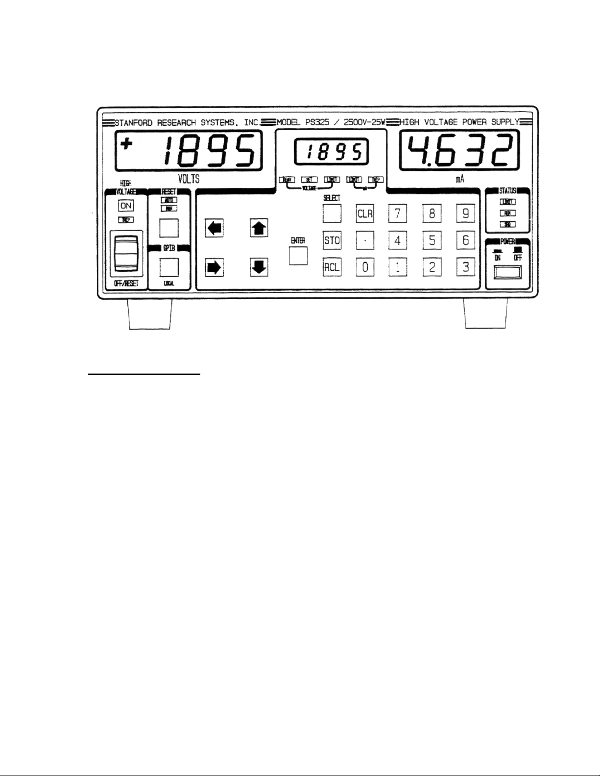
INSTRUMENT OVERVIEW
Front Panel Su m mary
Power Button
The PS300 series are turned on by depressing the
POWER button. The unit always powers up with
the high voltage OFF. All instrument settings are
stored in nonvolatile memory and are saved when
power is turned off. The model number (310, 325,
or 350), firmware version, and serial number are
displayed when power is turned on. If an error
appears on power on, then the stored settings were
lost and the default settings are used. If the default
settings are desired, hold down the CLR (clear) key
while turning on the power.
High Voltage Enable Switch
This is a three position switch that performs several
functions. In the down position, the high voltage is
off and all trips are cleared. In this position the
high voltage is locked OFF and cannot be turned
on by computer control. The up position is
momentary and turns on the high voltage for
manual or rear panel analog control. In the middle
position the high voltage is enabled (but not
necessarily on) and can be turned on by computer.
The large red LED above the switch indicates that
the high voltage is on; the yellow LED below it
indicates a trip has occurred.
LED Displays
The two large displays show output voltage and
current to four significant places. Polarity is
displayed on the left of the voltage display. The
smaller center display shows the value of the
parameter that is being entered or adjusted. That
parameter is indicated by the row of LEDs directly
below the center display.
Select, Enter, and Clear
The SELECT key is used to choose which
parameter is being displayed in the center display.
The ENTER key enters the parameter shown in the
center display. The clear (CLR) key erases the
value in the middle display and recalls the last
value that was entered. To adjust a value, the
SELECT key is pressed until the appropriate LED
is lit. When the value is being changed, that LED
will flash to indicate that the value in the center
display is not the current unit setting. If an
incorrect value is entered, press CLR (clear) to start
over. When the desired value is in the center
display, pressing the ENTER key updates the unit's
actual setting and stops the LED's flashing.
7
Page 10

Numeric and Cursor Keys
Other Keys
All parameters may be adjusted using the cursor or
numeric keys. When using the cursors, the digit
being adjusted in the center display will flash. The
UP and DOWN keys increment and decrement the
digit. The LEFT and RIGHT keys select the
flashing digit. When using direct numerical entry,
simply press the number and decimal point keys
until the desired value appears on the center
display. Note that the current is specified in mA.
Instrument Status
Three LED's indicate the instrument's status. The
LIMIT LED is on when the unit is in current limit.
REM is on when the front panel is locked out.
SRQ is on when a GPIB service request is pending.
RESET sets the reset mode to either AUTO or
MAN (manual).
GPIB displays the GPIB address in the center
display so it can be adjusted. It is also the LOCAL
key when the unit is in the remote mode.
Store and Recall
STO (store) and RCL (recall) allow up to 9
complete instrument settings to be saved in
nonvolatile memory. RCL 0 recalls the default
settings.
8
Page 11
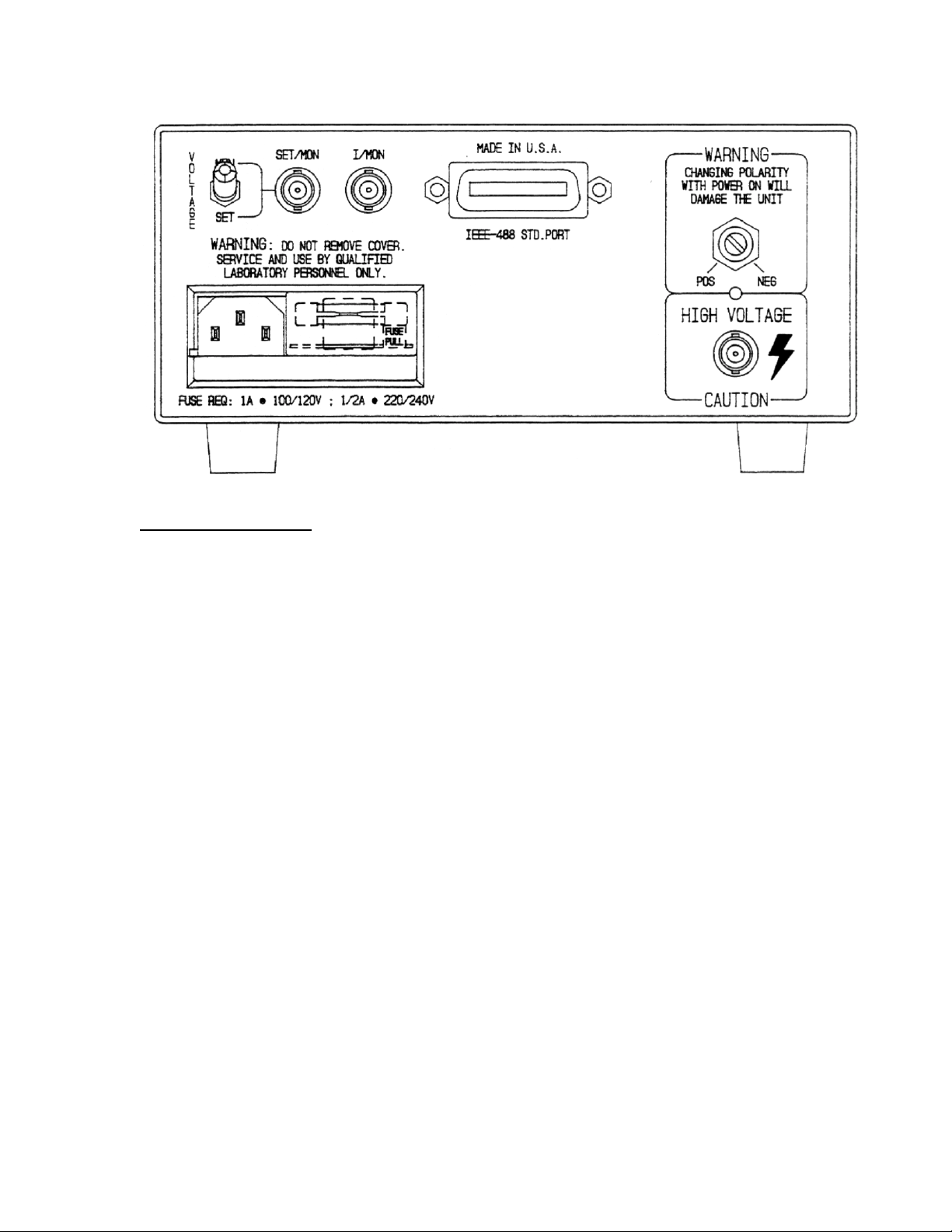
Rear Panel Summary
Power Entry Module
The power entry module is used to fuse the line,
select the line voltage, and block high frequency
noise from entering or exiting the unit. Refer to
the first page of the manual for instructions on
selecting the correct line voltage and fuse.
High Voltage Output Connector
WARNING: This unit contains hazardous
voltages. Please make certain that the high voltage
is completely discharged before removing or
connecting the high voltage cable. High voltage
cables can store charge if they are disconnected
from the supply while high voltage is present
which can cause injury or damage the unit.
The high voltage output connector is an SHV male
connector (Kings type 1704-1). Please make
certain that the high voltage is completely
discharged before changing the cable.
A 10 feet SHV-SHV or SHV-MHV cable is
available from SRS.
High Voltage Polarity Selector
WARNING: The unit must be turned off and the
high voltage should be completely discharged
before reversing the polarity. Failure to do this can
cause injury or damage the unit.
Polarity is indicated by the screwdriver slot on the
polarity switch as well as on the front panel's
voltage display. To reverse the polarity, turn the
unit off and allow the high voltage to completely
discharge. Then turn the polarity switch with a
large flathead screwdriver (clockwise for + to - and
counterclockwise for - to + ).
Analog Outputs
The two BNC's provide voltage and current
monitor signals, or an external voltage set and
current monitor. When the voltage select switch is
in the MON (monitor) position, both are 0 to +10
Volt outputs corresponding to 0 to full scale. When
the voltage select switch is in the SET position, the
current signal acts the same, but the voltage BNC
is an input, setting the the high voltage over the
same scale. When the switch is in the SET position,
the REAR LED on the front panel is lit, indicating
that the high voltage is under analog control and
cannot be adjusted from the keypad. All signals are
positive voltages, independent of output voltage
polarity.
9
Page 12

IEEE-488 Std Port (optional)
The 24 pin IEEE-488 (GPIB) connector allows
computer control of PS300 series supplies. The
address is set from the front panel using the GPIB
key.
10
Page 13

GUIDE TO OPERATION
Setting Output Voltage
The voltage set can be changed with the high
voltage on or off.
To set the high voltage output, press the SELECT
key until the VOLTAGE SET LED is lit. The
present value of the set voltage will be displayed in
the center window. To change the value, enter the
desired voltage by either the numeric or cursor
keys. After the new value has been entered into the
center display, press ENTER to update the output
voltage. The VOLTAGE SET LED will flash until
ENTER or CLR is pressed to remind you that the
displayed value is not the actual programmed
value. If an 'Err2' message appears (illegal
parameter entered), check the voltage limit to see
that it is greater than or equal to the desired set
voltage. Use the CLR key to clear any error
message.
If the REAR LED is lit, the high voltage is
programmed from the analog set input on the rear
panel. In this mode, when the center display is
showing VOLTAGE SET, the display is the
present programmed value of the high voltage and
cannot be adjusted from the front panel.
Setting Voltage Limit
The voltage limit is a protection feature to prevent
the output voltage from being set too high or
overshooting because of dramatic load changes.
The output voltage cannot be set higher than the
voltage limit. In addition, if the output ever
exceeds the limit by more than 10% of full scale,
the unit trips and the high voltage is disabled. If
this occurs, a 'VTRP'(voltage trip) message appears
in the middle display.
After a trip it is not necessary to clear the trip
before turning the high voltage back on. If it is
necessary to change a parameter before turning the
high voltage back on, pressing CLR or putting the
high voltage switch in the off position will clear the
trip.
To set the voltage limit, press the SELECT key
until the VOLTAGE LIMIT LED is lit. The present
value of the voltage limit is displayed in the center
window. Change it with either the numeric or
cursor keys and press ENTER to update the actual
limit value. If an 'Err2' message appears (illegal
parameter entered), check to see that the output
voltage is less than or equal to the voltage limit.
Setting Current Limit
Current limiting varies the output voltage to limit
the output current to less than or equal to the
programmed current limit value. When the unit is
current limited, the LIMIT LED is lit.
The current limit is set in the same fashion as the
voltage limit, by SELECTing the present value on
the center window, changing it and then
ENTERing the new value.
Setting Current Trip
The current trip shuts off the high voltage when the
output current exceeds the trip value. The current
trip value is set in the same fashion as the voltage
and current limits. After a current trip occurs, the
'ITRP' (current trip) message will appear in the
middle display. Current trips are cleared in the
same fashion as voltage trips.
Primary Trip
A PTRP (primary trip) message will occur if the
current through the primary side of the high
voltage transformer and the switching MOSFET's
exceeds about 5.3 Amps. This feature is included
to protect the transformer and FET's. The trip level
is not user programmable and may be cleared in the
same manner as the voltage and current trips. If
repeated PTRP's occur, see the troubleshooting
section.
Reset Mode
The reset mode determines how the unit responds
after a voltage or current trip.
MAN (manual) Mode: The high voltage remains
off after a trip and requires that the operator turn it
back on.
AUTO (automatic) Mode: The unit waits until
the output voltage has fallen to 1/50 of its full scale
value and then turns the high voltage back on. This
is useful when dealing with loads that occasionally
short circuit but recover after removing the high
voltage.
11
Page 14

Store and Recall
STO (store) and RCL (recall) allow up to 9
complete instrument setups to be saved. To store a
setup, press the STO key, followed by a number (1-
9) and then the ENTER key. To recall a setup,
press the RCL key, followed by a number (0-9) and
then the ENTER key. RCL 0 returns the setup to
the factory default. Whenever a setup is recalled,
the high voltage is turned off for safety. If an 'Err3'
(recall error) occurs, then that stored setup was lost
due to a memory error and must be re-entered.
Error Messages
The following error messages may appear in the
center display. The CLR key clears the errors.
and does not allow the rear panel voltage to set the
output above the voltage limit. If the rear panel
voltage is too high, the output voltage will stop at
the limit voltage.
Voltage Monitor/Set: When the Analog
Programming switch is in the MONITOR position,
the VOLTAGE BNC is a monitor output providing
0 to +10 Volts for 0 to full scale output regardless
of polarity. When the switch is in the SET position,
the BNC becomes an input over the same range.
An input of 0 to +10 Volts will program the high
voltage from 0 to full scale, regardless of polarity.
Current Monitor: This provides 0 to +10 Volts
out for 0 to full scale output regardless of the
output polarity.
Err1 Memory Error
Power on memory error of the unit's
last setup. Default setup is recalled.
Err2 Illegal Parameter Entered.
Err3 Stored Value Recall Error
The stored setup (from STO and
RCL) was lost.
Err4 Illegal Storage Address
STO 0 is reserved for default settings.
Err5 No GPIB Interface The unit does
not have the GPIB option so the
GPIB address cannot be set.
Err6 Syntax error over GPIB.
Err7 Illegal parameter entered over GPIB.
Parameter entered is out of range.
Err 8 GPIB Output queue full.
Analog Programming and Monitor
The rear panel voltage select switch determines
whether the output voltage is set from the front
panel or from the rear panel voltage input. If the
switch is in the MON (monitor) position, the front
panel will set the voltage. If the switch is in the
SET position, the rear panel voltage will set the
output voltage. When the switch is in the SET
position, the REAR (rear panel) LED is lit and the
output voltage being set by the rear panel is
displayed in the middle display when it is showing
VOLTAGE SET. The voltage limit is still active
If the switch position is changed while the high
voltage is on, the unit will shut the high voltage
off.
Default Setup
The factory default setup can be recalled by
pressing the CLR key while turning the unit on or
recalling setup 0 (RCL 0). The default setup is also
recalled after a power on memory error (ERR 1).
The default setups are shown below.
PS310 Voltage Set 0 V
Voltage Limit 1250 V
Current Limit 21 mA
Current Trip 21 mA
Reset Mode MAN
High Voltage OFF
GPIB Addr 14 (if applicable)
PS325 Voltage Set 0 V
Voltage Limit 2500 V
Current Limit 10.5 mA
Current Trip 10.5 mA
Reset Mode MAN
High Voltage OFF
GPIB Addr 14 (if applicable)
PS350 Voltage Set 0 V
Voltage Limit 5000 V
Current Limit 5.25 mA
Current Trip 5.25 mA
Reset Mode MAN
High Voltage OFF
GPIB Addr 14 (if applicable)
12
Page 15

GUIDE TO PROGRAMMING
Remote Programming
The PS300 series High Voltage Power Supplies
may be remotely programmed via the GPIB (IEEE-
488) interface. Any computer supporting this
interface may be used to program the PS300.
The PS300 supports the IEEE-488.1 (1978)
interface standard. Additionally, it also supports
the required common commands of the IEEE-488.2
(1987) Standard. Before attempting to
communicate with the PS300 over the GPIB
interface, the PS300's device address must be set.
The address is set from the front panel by pressing
the GPIB key and using the up and down arrow
keys to set the address to any number between 0
and 30. Pressing the ENTER key then sets the
selection.
Command Syntax
Communications with the PS300 use ASCII
characters. Commands may be in either UPPER or
lower case and may contain any number of
embedded space characters.
A command to the PS300 consists of a four
character command mnemonic, arguments if
necessary, and a command terminator. The
terminator is a linefeed <lf> or EOI. No command
processing occurs until a command terminator is
received. Command mnemonics beginning with an
asterisk "*" are IEEE-488.2 (1987) defined
common commands. Commands may require one
or more parameters. Multiple parameters are
separated by commas ",".
Multiple commands may be sent on one command
line by separating them by semicolons ";". The
difference between sending several commands on
the same line and sending several independent
commands is when a command line is parsed and
executed, the entire line is executed before any
other device action proceeds. This allows
synchronization to be achieved using the
synchronization commands.
There is no necessity to wait between commands.
The PS300 has a 256 character input buffer and
processes commands in the order received. If the
buffer fills up, the PS300 will hold off handshaking
on the GPIB. Similarly, the PS300 has a 256
character output buffer to store output until the host
computer is ready to receive it. If the output buffer
fills up, it is cleared and an error reported.
The present value of a particular parameter may be
determined by querying the PS300 for its value. A
query is formed by appending a question mark "?"
to the command mnemonic and omitting the
desired parameter from the command. If multiple
queries are sent on one command line (separated
by semicolons, of course), the answers will be
returned in a single response line with the
individual responses separated by semicolons. The
default response terminator that the PS300 sends
with any answer to a query is a linefeed plus EOI.
All commands return integer results except as
noted in individual command descriptions.
Examples:
VSET1.0E3<lf> sets VSET to 1000 V
VSET?<lf> queries the value of
VSET
*IDN? <lf> queries the device
identification (query, no
parameters)
VSET100.0;VSET? <lf> sets voltage to 100 V
and queries the voltage
Detailed Command List
The four letter mnemonic in each command
sequence specifies the command. The rest of the
sequence consists of parameters. Multiple
parameters are separated by commas. Commands
that may be queried have a question mark ? in
parentheses (?) after the mnemonic. Commands
that may ONLY be queried have a ? after the
mnemonic. Commands that MAY NOT be queried
have no?.
Output Control Commands
HVOF
The HVOF command turns the high voltage OFF.
HVON
The HVON command turns the high voltage ON
provided that the front panel high voltage switch is
not in the OFF position. If the switch is in the OFF
position, the high voltage is left off and an
13
Page 16

execution error is reported. This command also
automatically clears any voltage or current trips.
setting mode may only be changed by setting the
rear panel switch.
IOUT?
The IOUT? query returns the actual output current.
This is the same value as shown on the front panel
meter. Note: As with the front panel meters, this
value takes about a second to stabilize after a
change in current.
VOUT?
The VOUT? query returns the actual output
voltage. This is the same voltage as shown on the
front panel meter. The value returned is a floating
point value and includes the sign of the output
voltage. Note: As with the front panel meters, this
value takes about a second to stabilize after a
change in voltage.
Setting Control Commands
*RCL i
The *RCL command recalls stored setting i.
Setting 0 recalls the default settings. If the stored
setting is corrupted, an error is returned.
*SAV i
The *SAV command stores the present setup as
setting i. i may range from 1 to 9.
ILIM(?) x
TCLR
The TCLR command clears any voltage or current
trips.
TMOD(?) i
The TMOD command sets the trip reset mode. The
value i = 0 sets manual trip reset, while the value i
= 1 sets the trip reset mode to auto.
VLIM(?) x
The VLIM command sets the value of the voltage
limit to x where x is the value in Volts. The sign of
value x MUST match the PS300's polarity setting.
The VLIM? query returns the present VLIM
setting. As with front panel control, the VLIM
value must be greater than or equal to the VSET
value or an execution error will be returned.
VSET(?) x
The VSET command sets the value of the voltage
set to x if front panel control is enabled. If rear
panel control is enabled, an error is returned. The
value x is a number in the units of Volts and the
sign of the number MUST match the PS300's
polarity setting. The VSET? query returns the
current VSET value. As with front panel control,
the VSET value must be less than or equal to to
VLIM value or an execution error will be returned.
The ILIM command sets the value of the current
limit to x. The value x is a floating point value with
the units of Amps (e.g. 1 mA = 1E-3). The ILIM?
query returns the current limit setting.
ITRP(?) x
The ITRP command sets the value of the current
trip to x. The value x is a floating point value with
the units of Amps (e.g. 1 mA = 1E-3). The ITRP?
query returns the current trip setting.
SMOD?
The SMOD? query returns the VSET setting mode.
The value 0 means that the voltage value is
controlled by the front panel setting, while the
value 1 indicates that the output is controlled by the
rear panel voltage control input. Note that the
Interface Control Command
*RST
The *RST common command resets the PS300 to
its default configurations. It is the same as holding
down "CLR " at power on.
*IDN?
The *IDN common query returns the PS300's
device configuration. This string is in the format:
StanfordResearchSystems,PS3XX,serial number,
version number, where XX is the particular model
number, "serial number" is the serial number of the
particular unit, and "version number" is the 3 digit
firmware version number.
14
Page 17

Status Reporting Commands
*CLS
The *CLS common command clears all status
registers
*ESE (?) j
The *ESE common command sets the standard
status byte enable register. The parameter j is the
decimal value that the enable register is to be set to.
*ESR? {j}
such as SRQ on power up to be produced if
desired.
Serial Poll Status Byte
bit name
0 stable This indicates that the VSET or
1 v trip This indicates that a voltage trip
usage
ILIM value is stable. The value
depends on whether the PS300 's
in constant current or constant
voltage mode.
has occurred.
The *ESR common command reads the value of
the standard status register. If the parameter j is
present the value of bit j is returned. Reading this
register will clear it. Reading bit j will clear bit j
only.
*PSC (?) j
The *PSC common command sets the value of the
power-on status clear bit. If j = 1, the power on
status clear bit is set and all status registers and
enable registers are cleared on power up. If j = 0,
the bit is cleared and the status enable registers
maintain their values at power down. This allows
the production of a service request at power up, etc.
*SRE (?) j
The *SRE common command sets the value of the
serial poll enable register. The parameter j is the
decimal value that the register is to be set to.
*STB? {j}
The *STB? common query reads the value of the
serial poll byte. If the parameter j is present the
value of bit j is returned. Reading this register has
no effect on its value. It is just the summary of the
other status registers.
Status Reporting
2 itrip This indicates that a current trip
has occurred.
3 ilim This indicates that a current limit
condition has occurred.
4 MAV This indicates that the GPIB
output queue is non-empty.
5 ESB This indicates that an unmasked
bit in the standard status byte has
been set.
6RQS/ SRQ BIT.
MSS
7 hvon This indicates that the high
voltage is on.
The PS300 will make a service request (SRQ)
whenever one of these bits is set AND the
corresponding bit in the serial poll enable register
is set. Note that any status condition will produce
only one SRQ even if it is never cleared. The vtrip,
itrip and ilim bits are latched bits. They are set on
the occurrence of the appropriate event and stay set
until either the status byte is read or the *CLS
command is sent. This allows one to detect if a trip
condition has ever occurred. All of the other bits
indicate the current states of their respective
functions.
The PS300 reports on its status by means of two
status bytes: the serial poll byte, and the standard
status byte.
On power up, the PS300 may either clear all of its
status enable registers or maintain them in the state
they were in during power down. The action taken
is set by the *PSC command and allows things
15
Page 18

Standard Event Status By te
GPIB Error Messages
bit name
0 unused
1unused
2 Query Error set by an output queue
3 Recall Err set if a stored setting is
4 Execution Err set by an out of range
5 Command Err set by a command syntax
6 URQ set by any key press
7 PON set by power on
This status byte is defined by IEEE-488.2 (1987)
and is used primarily to report errors in commands
received over the communications interfaces. The
bits in this register stay set once set and are cleared
by reading them or by the *CLS command. If a bit
in the standard status register is set and the
corresponding bit in the standard status enable
register is set, then the ESB bit in the serial poll
register is set.
usage
overflow
corrupt
parameter, or noncompletion of some
command due to a condition
like overload
error or unrecognized
command.
The following error messages will appear on the
middle display if an error occurs due to a command
sent over GPIB:
Err6 Syntax Error over GPIB.
The command had an error in syntax or
was unrecognizable. A syntax error could
be a misspelling of a command or
forgetting to include a '-' when setting a
negative value for the voltage or voltage
limit. This error is the same as Command
Error, bit 5 of the Standard Event Status
Byte.
Err7 Illegal Parameter entered over GPIB.
A parameter was set out of range, or a
command could not be completed because
of an overload. This error is the same as
Execution Err, bit 4 of the Standard Event
Status Byte.
Err 8 GPIB Output Queue full.
The output queue overflowed and was
cleared. This could be due to querying the
unit repeatedly and not reading out all of
the characters, or a problem at the
recieving unit. This error is the same as
Query Error, bit 2 of the Standard Event
Status Byte.
16
Page 19

PROGRAM EXAMPLES
This section lists example programs which use the GPIB port to control the PS300. All of the programs do the
same thing, only the language is different. The programs set up the PS300 to ramp the output voltage from 0 to
1000 Volts while reading the output current.
Program Example 1:
IBM PC, Microsoft BASIC, Via GPIB
This program requires the Capital Equipment Corporation GPIB card for the IBM PC. It has firmware in ROM
to interface high level languages to the GPIB.
Subroutine calls in Microsoft BASIC are done to memory locations specified by the name of the subroutine.
The address is relative to the segment address specified by the DEF SEG statement preceding the CALL.
In this program, the CEC card's ROM starts at C000H, the system controller's address is 21, and the PS300 is at
GPIB address 23. Make sure the address in the unit is set correctly and that the HIGH VOLTAGE ENABLE
switch is not OFF.
10 'EXAMPLE PROGRAM TO RAMP THE PS300 HV OUTPUT AND READ THE CURRENT
20 'USING IBM PC BASIC AND THE CAPITAL EQUIPMENT CORP.
30 'GPIB INTERFACE CARD
40 '
50 '
60 'SET THE PS300 GPIB ADDR=23
70 '
80 DEF SEG = &HC000 'BASE ADDRESS OF CEC CARD
90 INIT=0: TRANSMIT=3: SEND=9: ENTER=21 'ADDRESSES OF CEC FIRMWARE ROUTINES
100 ADDR%=21: SYS%=0 'CONTROLLER ADDRESS
110 PS300%=23 'PS300 ADDRESS
120 '
130 'STRING DEFINITIONS
140 IN$="IFC UNT UNL REN MTA LISTEN 23 SDC" 'CLEAR PS300
150 HV$="HVON" 'HV ENABLE
160 CR$="*RST" 'RESET PS300
170 IR$="IOUT?" 'READ CURRENT
180 VS$="VSET" 'SET HV OUTPUT LEVEL
190 '
200 '
210 CALL INIT(ADDR%,SYS%) 'INIT CEC CARD
220 CALL TRANSMIT(IN$,STATUS%): GOSUB 480 'CLEAR INTERFACE
230 CALL TRANSMIT(CR$,STATUS%):GOSUB 480 'RESET PS300
240 '
250 X=0 'INITIAL VOLTAGE=0
260 '
270 CALL SEND(PS300%,HV$,STATUS%): GOSUB 480 'ENABLE HV
280 '
290 X = X+10 'INCREMENT OUTPUT BY 10V
300 PRINT "VOLTAGE = "; X;
310 P$=VS$ + STR$(X) 'MAKE VSET COMMAND STRING
320 CALL SEND(PS300%,P$,STATUS%):GOSUB 480
17
Page 20

330'
340 CALL SEND(PS300%,IR$,STATUS%):GOSUB 480 'QUERY CURRENT
350 ANS$=SPACE$(20) 'CLEAR RESULT STRING
360 CALL ENTER(ANS$,LENGTH%,PS300%,STATUS%):GOSUB 480 'READ CURRENT
370 N=VAL(ANS$) 'INTO VARIABLE N
380 PRINT " CURRENT = "; N 'PRINT VALUE
390 '
400 IF X<1000 THEN GOTO 290 'LOOP
410 STOP
420 '
480 'CHECK STATUS OF LAST GPIB COMMUNICATION FOR ERRORS
490 IF STATUS%=0 THEN RETURN 'STATUS OK
500 PRINT "GPIB ERROR STATUS CODE = ";STATUS% 'ELSE ERROR
510 STOP
18
Page 21

Program Example 2:
IBM PC, Microsoft C V4.0, Via GPIB
This program requires the Capital Equipment Corporation GPIB card for the IBM PC. It has firmware in ROM
to interface high level languages to the GPIB.
The header file MS-C488.H contains definitions of all of the CEC firmware routines which can be called from
C. Note that the order of arguments in the calls are reversed from those used by BASIC.
To use these routines, the large model must be used. Compile with the /AL/Ze switch and link with GPIBL.OBJ (on the CEC disk).
/* Compile with >MSC program name/AL/Ze;
link with GPIB-L.OBJ (on CEC disk)
include MS-C488.H
MS-C488.H defines all of the CEC firmware routines so that they
can be called from a C program. Remember that the order of the
arguments is REVERSED from the BASIC calls described in the manual.
Example program to ramp the PS300 output and read the current
using Microsoft C v4.0 (large model) and the Capital
Equipment Corp. GPIB interface card.
Set the PS300 for GPIB ADDR=23.
*/
#include <ms-c488.h>
#include <stdio.h>
char result[80];
main()
{
int i,status,ps300=23;
int my_address=21, system_controller=0;
char cmd[80], vstr[40];
float n;
float x;
initialize(&system_controller, &my_address); /* init GPIB controller */
/* clear interface */
transmit(&status, "IFC UNT UNL REN MTA LISTEN 23 SDC");
Statcheck(status);
/* reset PS300 */
TxGpib(ps300,"*RST");
x = 0; /* initial output value */
/* enable HV */
TxGpib(ps300,"HVON");
while (x<1000.0)
19
Page 22

do
{
x += 10.0; /* increment output voltage level */
sprintf(vstr, "VSET %7.1f",x); /* make VSET command string */
TxGpib(ps300,vstr); /* send command */
TxGpib(ps300,"IOUT?"); /*query current */
GetGpib(ps300); /* into result string */
if (!(sscanf(result,"%f",&n)))
Statcheck(255);
/* print level */
printf ("Voltage = %f current = %f\n",x,n);
}
}
/* ****************************************************** */
TxGpib(address,command) /* transmit a command to addressed device */
int address;
char *command;
{
int status;
char t_string[80];
sprintf(t_string, "UNT UNL MTA LISTEN %d DATA '%s' 10",address,command);
transmit(&status, t_string);
Statcheck(status);
}
/* ****************************************************** */
GetGpib(address) /* get result string from addressed device */
int address;
{
char r_string[40], temp[80];
int length, status;
sprintf(r_string, "UNT UNL MLA TALK %d",address);
transmit(&status, r_string); /* make device a talker */
Statcheck(status);
strcpy(temp, " "); /* clear result string */
receive(&status, &length, temp); /* get answer */
Statcheck(status);
strcpy(result, temp); /* move answer into global result string */
}
/* ****************************************************** */
Statcheck(status) /* check GPIB status */
int status;
{
if (status)
{
printf("GPIB error: status = %d",status);
exit();
}
}
20
Page 23

Program Example 3:
IBM PC, Microsoft C V4.0, Via GPIB
This program requires the National Instruments GPIB card for the IBM PC. It has firmware on board that
interfaces it to high level languages.
To interface the PS300 to a PC with the National Instruments card, the interface card and drivers must be
configured properly. The National Instruments card CANNOT be simply unpacked and put into your computer.
The card must be configured with jumpers and switches to set the I/O address and interrupt levels. You must
also run the program "IBCONF" to configure the resident GPIB driver for the card. Please refer to the National
Instruments manual for additional information.
Once all the hardware and GPIB drivers are properly configured, use the IBIC program. This terminal
emulation program allows you to send commands to the PS300 directly from your keyboard. If you cannot talk
to the PS300 from IBIC, your programs will not run.
The header file decl.h must be included and the file should be linked with the appropriate cib*.obj.
/*
Compile with >MSC program name/AL/Ze;
Link with the appropriate cib*.obj (on the Nat'l Inst disk)
Include decl.h.
Example program to set the PS325 to 1000 volts and read the
current using Microsoft C v4.0 (large model) and the National
instruments GPIB interface card.
*/
#include <stdio.h>
#include <stdlib.h>
#include <decl.h>
main();
{
int i,status,ps300;
float x;
char data[40];
/* get device ID for power supply */
ps325 = ibfind("PS325")
if (ps325<0)
{
printf ("Cannot find PS325; rerun IBCONF/n");
exit(0);
}
/* reset ps300 */
ibwrt (ps300,"*RST",4);
/* turn on high voltage */
ibwrt (ps300,"HVON",4);
/* set voltage to 1000 volts */
21
Page 24

ibwrt (ps300, "VSET1000",8);
/* read current */
ibwrt (ps300,"IOUT?",5);
ibrd (ps300,data,20);
/* print answer */
sscanf (data,"%f",&x);
printf ("Voltage = 1000 Current = %1f/n",x);
}
22
Page 25

TROUBLESHOOTING
Always make certain that the power entry module
is set for the correct line voltage and the correct
fuse is installed. The selected line voltage can be
seen through the window on the power entry
module. Verify that the line cord is plugged all the
way into the power entry module and the power
button on the front panel is pressed in.
Power on Reset
If the instrument turns on with odd combinations of
LEDs on, garbled displays, or is unresponsive to
the keyboard, the memory contents may have been
corrupted, causing the instrument to "hang". To
remedy the situation, turn the unit off and hold
down the CLR key while turning the power back
on. This causes the unit to initialize the memory
and load the default setup.
Stuck Keys
If the center display is filled with a particular
number (like 4444), or one particular message (like
Err2), and the keyboard is unresponsive, check to
see if a key is stuck down. If so, gently flick the
stuck key back to the center of its hole.
No High Voltage
3) Check the the REAR LED. If it is on, then the
high voltage is being programmed by the
analog set voltage input on the rear panel and
not by the front panel. If so, make sure the
rear panel switch is in the desired position.
Repeated Trips
Voltage Trips: This may occur if the load changes
too rapidly, causing the voltage to overshoot. Try
raising the voltage limit.
Current Trips: Disconnect the load and see if the
unit still trips. If it works with no load, there may
be a problem with the load. If it still trips, the unit
may be damaged. Please contact the factory for
further information.
Primary Trip: If repeated PTRP's occur, the
power supply may be damaged. Please contact the
factory for further information.
Rear Panel Voltage Set
If the output voltage is not correct, check the
REAR LED and rear panel switch to see that they
are in the SET mode. Also check that the voltage
limit is higher than the desired voltage.
Check to make sure that the HIGH VOLTAGE
LED is on. If the HIGH VOLTAGE LED is OFF,
check the following.
1) Make certain you hold down the high voltage
key for at least half a second. It is designed to
take a fairly long keypress to avoid having the
high voltage turned on accidentally by
bumping into the switch.
2) Check the voltage limit and current trip levels
to see that they are not too low for your load.
If the HIGH VOLTAGE LED is ON but the output
voltage is zero or lower than expected, check the
following.
1) Check if the LIMIT LED is on. If so, the
current limit value could be too low or the load
could be drawing excessive current.
2) Make sure the voltage limit is as large or
larger than the desired output voltage.
Front Panel Tes t
Hold down the ENTER key while turning on the
unit to run the front panel test. After power is
turned on, one segment of one numerical digit
should be lit. By pressing the UP arrow key, step
through all 8 segments of this digit and the
following one. This verifies that all of the segment
drivers are functional. On the next UP keypress, all
segments and one of the single LED's should be lit.
By repeatedly pressing the UP key, all of the single
LED's can be turned on, one at a time. The keypad
can then be tested by pressing each key and
observing the key code on the display. The codes
increase from top to bottom and left to right. After
this test, turn the power off and restart the
instrument.
23
Page 26

Calibration
The calibration parameters are determined by a
computer aided calibration procedure after burn-in
at the factory. These values are stored in the
permanent memory of each unit. Because of this
there are no user adjustable components to
calibrate.
24
Page 27

CIRCUIT DESCRIPTION
Introduction
Schematics for the PS300 series supplies are shown
on the following pages. They include the
following: Voltage Control (page 1/11), Low
voltage pre-regulator and high frequency inverter
(page 2/11), Limits and Trip Circuitry (page 3/11),
A/D and D/A (page 4/11), the Microprocessor
(page 5/11), GPIB and Front Panel Control (page
6/11), Low Voltage Power Supplies (page 7/11),
Front Panel (page 8/11), and the High Voltage
Sections (page 9/11 through 11/11).
Most of the components are located on the main
circuit board. The front panel and high voltage
section are located on separate boards. In addition,
the high voltage board is covered with an acrylic
coating and enclosed in a protective box.
Voltage Control
Since the output is transformer coupled, only the
magnitude can be set by the primary side control
circuitry. The polarity must be set in the high
voltage section by a multi-pole switch. However,
the sensed voltage and current vary with polarity
and must be converted to a unipolar signal before
they can be used to control the output. To minimize
the effects of noise, the sensed voltage and current
are converted to a -8.26 to +8.26 V range (-8.26 V
corresponding to 0 volts out, +8.26 to full scale).
This allows 13 bits of resolution from the D/A over
±10 V with a relatively large bit size of 2.5 mV.
The sensed voltage, V SENSE (coming from a
resistive divider in the high voltage section) is
buffered by a high input impedance differential
amplifier made up of U109A, U109B and U101D.
This provides a 0 to +8.26 V signal. Next the
polarity is set (for positive or negative output
voltages) with a programmable low offset inverter
(U102, U104A and U104B) and then scaled to
±8.26 V. Next, the voltage is compared to the
programmed voltage with U101B. This signal is
then frequency compensated (U108, U101C, and
related R's and C's) to provide an error voltage, V
ERR. D104 and D107 keep the large capacitors in
the frequency compensation circuitry from
saturating.
The sensed current is first amplified by U105 from
0 - 250 mV to 0 to +8.26 V. Next, the polarity is
set by the programmable inverter of U104C,
(page 1/11)
U104D and U106. It is scaled to ±8.26 V by
U107C. Then it is compared and frequency
compensated at U107B, to provide I ERR.
D102 acts as a crossover between the two error
signals to determine which one sets V DRIVE, the
control for the output voltage. If I ERR is higher
than V ERR (voltage control mode), then V ERR
controls V DRIVE. However if I ERR is lower
(supply is in current limit), it can pull down V
DRIVE(through D102) to the appropriate level,
since V ERR is isolated by R110.
Diodes D105 and D106 act to keep op amps
U101C and U107B out of saturation during large
load changes. This improves transient response.
Low Voltage Pre-Regulator and HIgh
Frequency Inverter
High voltage is made with a high frequency DC to
DC converter. It operates by driving the common
tap of a step-up transformer used as an inverter,
from 0 to 35 volts DC. This makes high voltage by
a combination of transformation and voltage
multiplication. Control is achieved by regulating
the common tap.
Pre-Regulator
The common voltage is made by a combination
step down pre-regulator followed by a
programmable linear regulator. Q203, D203, L201
and C203 form the step down regulator and U205
is the linear regulator.
U206, an LM311 comparator, senses the voltage
across U205. If it is less than 2.5 volts (determined
by D204, a 2.5 volt reference), its output goes
negative. This turns on Q203, allowing current to
flow through L201 onto C203, raising the voltage
at the input of U205. Once the voltage across U205
is greater than 2.5 volts (plus a small amount of
hysteresis set by R219 and C205), U206 shuts off
Q203. Current continues to flow through L201
during the off time since current can't change
instantly through an inductor. This causes the
voltage at pin 2 of Q203 to flyback negatively and
be clamped by D203. The voltage across U205 will
now decay until it is less than 2.5 volts, which
begins the cycle again.
(page 2/11)
25
Page 28

U205, a LT1085, is a low dropout adjustable
regulator which filters the output of the step down
section. U207 increases the V DRIVE signal of 012 volts to 0-33 volts which programs the common
tap of the step-up high voltage transformer.
Inverter
U201 is a LM555 timer configured as an astable
multivibrator at a frequency of 40 kHz with about a
60% duty cycle. U202 and U203 split this into two
phases of 20 kHz at a 30% duty cycle. U204
(SN75372) is a high current MOSFET driver for
the FETs (Q201,Q202) that drive the high voltage
step-up transformer (pages 9/11 through 11/11).
D201 and D202 clamp excessive inductive flyback
voltage.
If the primary current exceeds about 5.3 amps,
R212 - R215 and U301C sense the primary side
current and shut off the drive to the inverter (and
hence the high voltage). They do this by activating
the HV OFF line (page 3/11), which latches the
high voltage off until the processor releases it. The
high voltage can also be turned off by voltage or
current trips and by the processor.
Limits and Trips
U301 is a quad comparator that compares both the
scaled output voltage and current to both the limit
and trip values which are set by the processor and
D/A. If a trip value is exceeded, the high voltage is
shut off through the HV OFF signal and the change
of status is reported to the processor. If a limit is
exceeded, only the change of status is reported.
The processor can also set the HV OFF line via the
SHUTDOWN line.
U306 is a one-shot circuit used as a watch dog
timer. Unless the microprocessor resets it every 10
ms, the one-shot times out, turning off the high
voltage and forcing a system reset.
A/D's and D/A's
U410 is a 12 bit digital to analog converter that is
loaded 4 bits at a time from the processor. Its
output current is converted to a voltage by U402B
to provide a 0 to -10.00 VDC referenced from
LH0070 (U406), a precision reference. U407A,
U407B and U405 form a programmable low offset
inverter. After scaling, the output covers a range of
-10.24 to +10.24 VDC with 13 bits of resolution
and 2.5 mV bits. These outputs are multiplexed to
(page 3/11)
(page 4/11)
6 sample and hold circuits that provide control
voltages and outputs. Each sample and hold is
refreshed every 12 ms.
U402A and U404 form an integrating, successive
approximation analog to digital converter. U409
determines the input to be sampled and integrates it
through R404 on to C401. Then a successive
approximation 13 bit analog to digital conversion is
made using the D/A converter and comparator
U404. This takes about 100 µs.
Microprocessor Control
The microprocessor, U501 (a Z80), is clocked at 4
MHz by X501. U502, an 8K ROM, contains the
firmware and calibration constants. The 2K static
RAM, U503, is backed up by a lithium battery,
BT501. A power down circuit protects the RAM
contents by disabling the chip-select with Q501 if a
reset is asserted. The battery should have a useful
life of 5 to 10 years and shouldn't need to be
replaced.
U504 and U505 generate chip selects for the
various input and output ports. U506 and U512 are
input ports for status information, rear panel
switches, and the HV ON/OFF switch on the front
panel.
U509 and related parts form the power on reset
circuit. During power on, it asserts a reset for
about 250 ms so the supply voltages can stabilize.
If the +5 V power supply dips below 4.5 V
(determined by the +10.00 V reference), it asserts a
reset that will last until the voltage recovers and a
reset cycle has occurred. If the watch dog timer
isn't updated every 10 ms, it triggers U511, which
also forces a reset. During a reset, in addition to
the processor being reset and the RAM being
disabled, the high voltage is turned off.
(page 5/11)
GPIB and Front Panel Interface
(page 6/11)
GPIB
The GPIB (IEEE-488) interface is provided by the
TMS9914A controller, U601. U602 and U603 are
buffers to the GPIB connector, which is connected
to J602. U601 is programmed to interrupt the
processor whenever there is activity addressed to
the power supply.
26
Page 29

Front Panel Interface
Front Panel
(page 8/11)
The front panel has a 6 phase, multiplexed LED
display and keyboard. U604 is a data bus latch for
U605, a high current driver that provides the strobe
signals to the front panel. Each strobe selects 2
digits and 2 or 3 LED's to be refreshed. Only one
strobe is active at a time. U606 and U609 are pull
down lines for the digits with 390 Ohm current
limiting resistors (N601 and N602). The individual
LEDs are pulled down separately by U613AU613C with 12 Ohm current limiting
resistors(R602-R604). They are separated from the
digit pulldowns because the LED's require much
more current than the high efficiency 7 segment
displays. Strobes 2, 3 and 4 also go to the keypad
matrix which is read by U612, an input latch.
U610, a divider chip, takes the system clock of 4
MHz and divides it by 4096 which gives a 977 Hz
signal. This provides the processor with a a real
time interrupt which is used to synchronize
updating the display, analog voltages, and
instrument status.
Low Voltage Power Supplies
(page 7/11)
The front panel consists of twelve 7 segment high
efficiency displays, a ±1 display, 13 LED's, a
keypad and the high voltage on/off switch.
The displays are multiplexed by 6 strobes. During
each strobe, two of the twelve displays are on. In
addition, up to 2 (of a maximum of 3) LEDs are on
to indicate the instrument status and polarity. The
±1 display is driven the same as the LEDs, but it
has larger current limiting resistors R1 and R2 (390
Ohms), since it is far more efficient then the
ordinary LEDs. Finally strobes 2, 3 and 4 go to the
keypad matrix allowing 1/3 of the keys to be read
during each of these strobe cycles.
The High Voltage ON/OFF switch is separate from
the keypad matrix. Its signals go directly back to
one of the processor's input ports.
High Voltage Section
Note: These boards are covered to prevent
accidental shock or injury. DO NOT ATTEMPT
TO OPERATE THE UNIT WITH THE COVER
OFF !!!
Line power comes in at the power entry module
where it passes through a fuse and then a RFI filter.
Both the hot and neutral leads are switched. Next,
the voltage passes into the line voltage selector.
The transformer primary is tapped for 4 different
voltages: 100,120, 220, 240 VAC, 50 or 60 Hz.
The transformer has 3 secondaries, 32 VAC non
centertapped and 32 VAC and 15 VAC, center
tapped. The 15 volt tap is rectified by D703 and
D704. It is filtered by C706 to make +8 VDC
unregulated. Then it is regulated by U704 to make
the +5 VDC for the processor, digital logic. U707
regulates the +5VDC for the LED display. The 32
volt tap is full wave rectified by U701 and filtered
by C702 and C705 to provide ±18 VDC. These are
regulated by U702 and U703 to make ±15 VDC for
the analog circuitry.
The 32 volt non center tapped winding is rectified
by D701 and D702, and filtered by C701. It
provides +35 VDC at 1 amp to the pre-regulator for
the high voltage section. U705 provides a regulated
+33 VDC for the control circuits in the preregulator.
PS310 (page 9/11)
The biggest difference between models in the
PS300 series is the high voltage section. They are
configured to provide the proper combination of
voltage and current through the use of different
diode-capacitor multiplier circuits. For the PS310
(page 9/11), the output of transformer T1 is full
wave rectified by diodes D1-D4 and filtered by C3
and C4. Poles A and B of switch SW1 change the
polarity of the high voltage output and pole C
reports the polarity to the processor. C3, C4 and
R1-R3 are an output filter to reduce switching
noise. R4, R5 and R8 form the divider to provide
the voltage sense signal; R6 and R9 are the current
sense resistor.
PS325 (page 10/11)
The PS325 (page 10/11) is similar to the PS310
except the transformer output is fed to the voltage
doubling circuit of D1, D2, C1 and C2. Switch
SW1 acts in the same fashion as on the PS310.
The voltage sense circuit consists of R4, R5, R6
and R8. R7 and R9 are the current sense resistor.
The output filter is slightly different to reflect the
changes in output voltage and current.
27
Page 30

PS350 (page 11/11)
The PS350 (page 11/11) is similar to the other two,
but it has a voltage quadrupler made up of C1, C2,
C3, C4, D1, D2, D3 and D4. Switch SW1 acts the
same and R9 is again the current sense resistor.
The voltage sense circuit is made up of R2 and R3.
C5 provides some additional phase compensation.
Finally the output filter is set up for higher voltage
and lower current.
28
Page 31

COMPONENT LIST
Main Board Parts List
No. REF. SRS part # VALUE DESCRIPTION
1. BT501 6-00001-612
2. C 101 5-00066-513 .022U Capacitor, Mylar/Poly, 50V, 5%, Rad
3. C 102 5-00023-529 .1U Cap, Monolythic Ceramic, 50V, 20%, Z5U
4. C 103 5-00023-529 .1U Cap, Monolythic Ceramic, 50V, 20%, Z5U
5. C 104 5-00190-541 100U MIN Cap, Mini Electrolytic, 16V, 20% Radial
6. C 105 5-00264-513 .0015U Capacitor, Mylar/Poly, 50V, 5%, Rad
7. C 107 5-00059-512 .47U Cap, Stacked Metal Film 50V 5% -40/+85c
8. C 109 5-00264-513 .0015U Capacitor, Mylar/Poly, 50V, 5%, Rad
9. C 110 5-00335-513 .0039U Capacitor, Mylar/Poly, 50V, 5%, Rad
10. C 111 5-00100-517 2.2U Capacitor, Tantalum, 35V, 20%, Rad
11. C 112 5-00058-512 .33U Cap, Stacked Metal Film 50V 5% -40/+85c
12. C 113 5-00067-513 .033U Capacitor, Mylar/Poly, 50V, 5%, Rad
13. C 114 5-00060-512 1.0U Cap, Stacked Metal Film 50V 5% -40/+85c
14. C 115 5-00264-513 .0015U Capacitor, Mylar/Poly, 50V, 5%, Rad
15. C 116 5-00100-517 2.2U Capacitor, Tantalum, 35V, 20%, Rad
16. C 201 5-00023-529 .1U Cap, Monolythic Ceramic, 50V, 20%, Z5U
17. C 202 5-00064-513 .0047U Capacitor, Mylar/Poly, 50V, 5%, Rad
18. C 203 5-00176-509 3300U Capacitor, Electrolytic, 50V, 20%, Rad
19. C 204 5-00041-509 220U Capacitor, Electrolytic, 50V, 20%, Rad
20. C 205 5-00151-501 680P Capacitor, Ceramic Disc, 50V, 10%, SL
21. C 206 5-00012-501 330P Capacitor, Ceramic Disc, 50V, 10%, SL
22. C 207 5-00100-517 2.2U Capacitor, Tantalum, 35V, 20%, Rad
23. C 208 5-00100-517 2.2U Capacitor, Tantalum, 35V, 20%, Rad
24. C 209 5-00100-517 2.2U Capacitor, Tantalum, 35V, 20%, Rad
25. C 210 5-00100-517 2.2U Capacitor, Tantalum, 35V, 20%, Rad
26. C 211 5-00100-517 2.2U Capacitor, Tantalum, 35V, 20%, Rad
27. C 212 5-00065-513 .01U Capacitor, Mylar/Poly, 50V, 5%, Rad
28. C 213 5-00065-513 .01U Capacitor, Mylar/Poly, 50V, 5%, Rad
29. C 215 5-00065-513 .01U Capacitor, Mylar/Poly, 50V, 5%, Rad
30. C 216 5-00065-513 .01U Capacitor, Mylar/Poly, 50V, 5%, Rad
31. C 217 5-00065-513 .01U Capacitor, Mylar/Poly, 50V, 5%, Rad
32. C 218 5-00065-513 .01U Capacitor, Mylar/Poly, 50V, 5%, Rad
33. C 219 5-00127-524 2.2U Capacitor, Tantalum, 50V, 20%, Rad
34. C 220 5-00023-529 .1U Cap, Monolythic Ceramic, 50V, 20%, Z5U
35. C 301 5-00065-513 .01U Capacitor, Mylar/Poly, 50V, 5%, Rad
36. C 302 5-00065-513 .01U Capacitor, Mylar/Poly, 50V, 5%, Rad
37. C 303 5-00007-501 220P Capacitor, Ceramic Disc, 50V, 10%, SL
38. C 304 5-00023-529 .1U Cap, Monolythic Ceramic, 50V, 20%, Z5U
39. C 401 5-00136-519 .01U Capacitor, Polystyrene, 50V, 5%, Rad
40. C 402 5-00007-501 220P Capacitor, Ceramic Disc, 50V, 10%, SL
41. C 405 5-00061-513 .001U Capacitor, Mylar/Poly, 50V, 5%, Rad
42. C 406 5-00008-501 22P Capacitor, Ceramic Disc, 50V, 10%, SL
43. C 407 5-00023-529 .1U Cap, Monolythic Ceramic, 50V, 20%, Z5U
44. C 408 5-00061-513 .001U Capacitor, Mylar/Poly, 50V, 5%, Rad
45. C 409 5-00023-529 .1U Cap, Monolythic Ceramic, 50V, 20%, Z5U
46. C 410 5-00023-529 .1U Cap, Monolythic Ceramic, 50V, 20%, Z5U
VALUE
Battery
29
Page 32

No.
REF. SRS part # VALUE DESCRIPTION
47. C 411 5-00023-529 .1U Cap, Monolythic Ceramic, 50V, 20%, Z5U
48. C 412 5-00023-529 .1U Cap, Monolythic Ceramic, 50V, 20%, Z5U
49. C 413 5-00023-529 .1U Cap, Monolythic Ceramic, 50V, 20%, Z5U
50. C 414 5-00023-529 .1U Cap, Monolythic Ceramic, 50V, 20%, Z5U
51. C 415 5-00023-529 .1U Cap, Monolythic Ceramic, 50V, 20%, Z5U
52. C 501 5-00007-501 220P Capacitor, Ceramic Disc, 50V, 10%, SL
53. C 502 5-00007-501 220P Capacitor, Ceramic Disc, 50V, 10%, SL
54. C 503 5-00098-517 10U Capacitor, Tantalum, 35V, 20%, Rad
55. C 504 5-00023-529 .1U Cap, Monolythic Ceramic, 50V, 20%, Z5U
56. C 505 5-00023-529 .1U Cap, Monolythic Ceramic, 50V, 20%, Z5U
57. C 506 5-00023-529 .1U Cap, Monolythic Ceramic, 50V, 20%, Z5U
58. C 601 5-00098-517 10U Capacitor, Tantalum, 35V, 20%, Rad
59. C 701 5-00241-553 3900U Capacitor, Electrolytic, 80V, +/-20%
60. C 702 5-00172-544 1000U Cap, Mini Electrolytic, 25V, 20%, Radial
61. C 703 5-00192-542 22U MIN Cap, Mini Electrolytic, 50V, 20% Radial
62. C 704 5-00100-517 2.2U Capacitor, Tantalum, 35V, 20%, Rad
63. C 705 5-00172-544 1000U Cap, Mini Electrolytic, 25V, 20%, Radial
64. C 706 5-00192-542 22U MIN Cap, Mini Electrolytic, 50V, 20% Radial
65. C 707 5-00100-517 2.2U Capacitor, Tantalum, 35V, 20%, Rad
66. C 708 5-00169-520 4700U Capacitor, Electrolytic, 16V, 20%, Rad
67. C 709 5-00192-542 22U MIN Cap, Mini Electrolytic, 50V, 20% Radial
68. C 710 5-00100-517 2.2U Capacitor, Tantalum, 35V, 20%, Rad
69. C 711 5-00213-546 4.7U Cap, Mini Electro, 100V, 20%, Rad
70. C 712 5-00214-547 .1U Cap, Monolythic Ceramic, 100V, Z5U, 20%
71. C 713 5-00127-524 2.2U Capacitor, Tantalum, 50V, 20%, Rad
72. C 714 5-00127-524 2.2U Capacitor, Tantalum, 50V, 20%, Rad
73. C 715 5-00023-529 .1U Cap, Monolythic Ceramic, 50V, 20%, Z5U
74. C 716 5-00023-529 .1U Cap, Monolythic Ceramic, 50V, 20%, Z5U
75. C 717 5-00023-529 .1U Cap, Monolythic Ceramic, 50V, 20%, Z5U
76. C 718 5-00023-529 .1U Cap, Monolythic Ceramic, 50V, 20%, Z5U
77. C 719 5-00023-529 .1U Cap, Monolythic Ceramic, 50V, 20%, Z5U
78. C 720 5-00023-529 .1U Cap, Monolythic Ceramic, 50V, 20%, Z5U
79. C 721 5-00023-529 .1U Cap, Monolythic Ceramic, 50V, 20%, Z5U
80. C 722 5-00225-548 .1U AXIAL Capacitor, Ceramic, 50V,+80/-20% Z5U AX
81. C 724 5-00023-529 .1U Cap, Monolythic Ceramic, 50V, 20%, Z5U
82. C 725 5-00023-529 .1U Cap, Monolythic Ceramic, 50V, 20%, Z5U
83. C 726 5-00225-548 .1U AXIAL Capacitor, Ceramic, 50V,+80/-20% Z5U AX
84. C 727 5-00023-529 .1U Cap, Monolythic Ceramic, 50V, 20%, Z5U
85. C 728 5-00023-529 .1U Cap, Monolythic Ceramic, 50V, 20%, Z5U
86. C 729 5-00023-529 .1U Cap, Monolythic Ceramic, 50V, 20%, Z5U
87. C 730 5-00023-529 .1U Cap, Monolythic Ceramic, 50V, 20%, Z5U
88. C 731 5-00023-529 .1U Cap, Monolythic Ceramic, 50V, 20%, Z5U
89. C 732 5-00023-529 .1U Cap, Monolythic Ceramic, 50V, 20%, Z5U
90. C 733 5-00023-529 .1U Cap, Monolythic Ceramic, 50V, 20%, Z5U
91. C 734 5-00023-529 .1U Cap, Monolythic Ceramic, 50V, 20%, Z5U
92. C 735 5-00023-529 .1U Cap, Monolythic Ceramic, 50V, 20%, Z5U
93. C 736 5-00023-529 .1U Cap, Monolythic Ceramic, 50V, 20%, Z5U
94. C 737 5-00023-529 .1U Cap, Monolythic Ceramic, 50V, 20%, Z5U
95. C 738 5-00023-529 .1U Cap, Monolythic Ceramic, 50V, 20%, Z5U
96. C 739 5-00023-529 .1U Cap, Monolythic Ceramic, 50V, 20%, Z5U
97. C 740 5-00219-529 .01U Cap, Monolythic Ceramic, 50V, 20%, Z5U
30
Page 33

No.
REF. SRS part # VALUE DESCRIPTION
98. C 741 5-00219-529 .01U Cap, Monolythic Ceramic, 50V, 20%, Z5U
99. C 742 5-00219-529 .01U Cap, Monolythic Ceramic, 50V, 20%, Z5U
100. CX111 5-00098-517 10U Capacitor, Tantalum, 35V, 20%, Rad
101. CX116 5-00098-517 10U Capacitor, Tantalum, 35V, 20%, Rad
102. D 101 3-00004-301 1N4148 Diode
103. D 102 3-00004-301 1N4148 Diode
104. D 104 3-00004-301 1N4148 Diode
105. D 105 3-00004-301 1N4148 Diode
106. D 106 3-00004-301 1N4148 Diode
107. D 107 3-00004-301 1N4148 Diode
108. D 201 3-00221-301 1N4004 Diode
109. D 202 3-00221-301 1N4004 Diode
110. D 203 3-00228-301 MUR160 Diode
111. D 204 3-00291-340 LM336Z-2.5V Integrated Circuit (Thru-hole Pkg)
112. D 205 3-00004-301 1N4148 Diode
113. D 207 3-00380-301 1N5248 Diode
114. D 208 3-00221-301 1N4004 Diode
115. D 209 3-00380-301 1N5248 Diode
116. D 210 3-00381-301 SA64A Diode
117. D 211 3-00381-301 SA64A Diode
118. D 212 3-00390-301 1N969A/1N5251B Diode
119. D 501 3-00004-301 1N4148 Diode
120. D 502 3-00004-301 1N4148 Diode
121. D 503 3-00004-301 1N4148 Diode
122. D 703 3-00221-301 1N4004 Diode
123. D 704 3-00221-301 1N4004 Diode
124. J 401 1-00073-120 INSL Connector, BNC
125. J 402 1-00073-120 INSL Connector, BNC
126. J 601 1-00081-110 554434-1 SHIELD Pins & Connectors, AMP
127. J 602 1-00038-130 40 PIN DIL Connector, Male
128. J 603 1-00097-130 24 PIN DIL Connector, Male
129. L 201 6-00044-601 750UH Inductor
130. N 101 4-00333-421 10KX5 Res. Network, SIP, 1/4W,2% (Isolated)
131. N 103 4-00333-421 10KX5 Res. Network, SIP, 1/4W,2% (Isolated)
132. N 104 4-00244-421 10KX4 Res. Network, SIP, 1/4W,2% (Isolated)
133. N 301 4-00334-425 10KX5 Resistor Network SIP 1/4W 2% (Common)
134. N 501 4-00244-421 10KX4 Res. Network, SIP, 1/4W,2% (Isolated)
135. N 502 4-00334-425 10KX5 Resistor Network SIP 1/4W 2% (Common)
136. N 601 4-00420-420 390X8 Resistor Network, DIP, 1/4W,2%,8 Ind
137. N 602 4-00420-420 390X8 Resistor Network, DIP, 1/4W,2%,8 Ind
138. N 603 4-00276-425 10KX9 Resistor Network SIP 1/4W 2% (Common)
139. N 604 4-00285-421 470X3 Res. Network, SIP, 1/4W,2% (Isolated)
140. P 401 4-00657-452 500 Pot, Multi Turn Trim, Mini
141. PC1 7-00184-701 PS300-25 Printed Circuit Board
142. Q 201 3-00283-340 IRF530/IRF532 Integrated Circuit (Thru-hole Pkg)
143. Q 202 3-00283-340 IRF530/IRF532 Integrated Circuit (Thru-hole Pkg)
144. Q 203 3-00374-329 MTP20P06 Voltage Reg., TO-220 (TAB) Package
145. Q 501 3-00021-325 2N3904 Transistor, TO-92 Package
146. R 101 4-00450-407 681 Resistor, Metal Film, 1/8W, 1%, 50PPM
147. R 102 4-00194-407 5.11K Resistor, Metal Film, 1/8W, 1%, 50PPM
148. R 103 4-00185-407 4.02K Resistor, Metal Film, 1/8W, 1%, 50PPM
31
Page 34

No.
REF. SRS part # VALUE DESCRIPTION
149. R 104 4-00138-407 10.0K Resistor, Metal Film, 1/8W, 1%, 50PPM
150. R 105 4-00450-407 681 Resistor, Metal Film, 1/8W, 1%, 50PPM
151. R 110 4-00130-407 1.00K Resistor, Metal Film, 1/8W, 1%, 50PPM
152. R 111 4-00138-407 10.0K Resistor, Metal Film, 1/8W, 1%, 50PPM
153. R 112 4-00446-407 47.5K Resistor, Metal Film, 1/8W, 1%, 50PPM
154. R 113 4-00553-407 2.55K Resistor, Metal Film, 1/8W, 1%, 50PPM
155. R 114 4-00447-407 82.5K Resistor, Metal Film, 1/8W, 1%, 50PPM
156. R 115 4-00553-407 2.55K Resistor, Metal Film, 1/8W, 1%, 50PPM
157. R 116 4-00190-407 42.2K Resistor, Metal Film, 1/8W, 1%, 50PPM
158. R 117 4-00190-407 42.2K Resistor, Metal Film, 1/8W, 1%, 50PPM
159. R 119 4-00188-407 4.99K Resistor, Metal Film, 1/8W, 1%, 50PPM
160. R 122 4-00607-407 3.92K Resistor, Metal Film, 1/8W, 1%, 50PPM
161. R 123 4-00138-407 10.0K Resistor, Metal Film, 1/8W, 1%, 50PPM
162. R 124 4-00447-407 82.5K Resistor, Metal Film, 1/8W, 1%, 50PPM
163. R 125 4-00192-407 49.9K Resistor, Metal Film, 1/8W, 1%, 50PPM
164. R 201 4-00483-407 1.05K Resistor, Metal Film, 1/8W, 1%, 50PPM
165. R 202 4-00309-407 3.32K Resistor, Metal Film, 1/8W, 1%, 50PPM
166. R 203 4-00034-401 10K Resistor, Carbon Film, 1/4W, 5%
167. R 204 4-00138-407 10.0K Resistor, Metal Film, 1/8W, 1%, 50PPM
168. R 205 4-00176-407 3.01K Resistor, Metal Film, 1/8W, 1%, 50PPM
169. R 206 4-00135-407 1.50K Resistor, Metal Film, 1/8W, 1%, 50PPM
170. R 207 4-00851-407 340 Resistor, Metal Film, 1/8W, 1%, 50PPM
171. R 208 4-00138-407 10.0K Resistor, Metal Film, 1/8W, 1%, 50PPM
172. R 209 4-00176-407 3.01K Resistor, Metal Film, 1/8W, 1%, 50PPM
173. R 210 4-00135-407 1.50K Resistor, Metal Film, 1/8W, 1%, 50PPM
174. R 212 4-00364-402 1 Resistor, Carbon Comp, 1/2W, 5%
175. R 213 4-00364-402 1 Resistor, Carbon Comp, 1/2W, 5%
176. R 214 4-00364-402 1 Resistor, Carbon Comp, 1/2W, 5%
177. R 215 4-00364-402 1 Resistor, Carbon Comp, 1/2W, 5%
178. R 216 4-00138-407 10.0K Resistor, Metal Film, 1/8W, 1%, 50PPM
179. R 217 4-00138-407 10.0K Resistor, Metal Film, 1/8W, 1%, 50PPM
180. R 218 4-00547-407 18.2K Resistor, Metal Film, 1/8W, 1%, 50PPM
181. R 219 4-00192-407 49.9K Resistor, Metal Film, 1/8W, 1%, 50PPM
182. R 220 4-00548-407 29.4K Resistor, Metal Film, 1/8W, 1%, 50PPM
183. R 221 4-00138-407 10.0K Resistor, Metal Film, 1/8W, 1%, 50PPM
184. R 222 4-00080-401 47 Resistor, Carbon Film, 1/4W, 5%
185. R 223 4-00080-401 47 Resistor, Carbon Film, 1/4W, 5%
186. R 224 4-00045-401 2.0K Resistor, Carbon Film, 1/4W, 5%
187. R 301 4-00021-401 1.0K Resistor, Carbon Film, 1/4W, 5%
188. R 302 4-00021-401 1.0K Resistor, Carbon Film, 1/4W, 5%
189. R 303 4-00312-401 270K Resistor, Carbon Film, 1/4W, 5%
190. R 304 4-00021-401 1.0K Resistor, Carbon Film, 1/4W, 5%
191. R 305 4-00021-401 1.0K Resistor, Carbon Film, 1/4W, 5%
192. R 306 4-00021-401 1.0K Resistor, Carbon Film, 1/4W, 5%
193. R 307 4-00021-401 1.0K Resistor, Carbon Film, 1/4W, 5%
194. R 308 4-00069-401 300K Resistor, Carbon Film, 1/4W, 5%
195. R 401 4-00021-401 1.0K Resistor, Carbon Film, 1/4W, 5%
196. R 402 4-00021-401 1.0K Resistor, Carbon Film, 1/4W, 5%
197. R 403 4-00034-401 10K Resistor, Carbon Film, 1/4W, 5%
198. R 404 4-00164-407 20.0K Resistor, Metal Film, 1/8W, 1%, 50PPM
199. R 409 4-00022-401 1.0M Resistor, Carbon Film, 1/4W, 5%
32
Page 35

No.
REF. SRS part # VALUE DESCRIPTION
200. R 410 4-00170-407 249K Resistor, Metal Film, 1/8W, 1%, 50PPM
201. R 411 4-00196-407 6.04K Resistor, Metal Film, 1/8W, 1%, 50PPM
202. R 412 4-00034-401 10K Resistor, Carbon Film, 1/4W, 5%
203. R 413 4-00138-407 10.0K Resistor, Metal Film, 1/8W, 1%, 50PPM
204. R 414 4-00138-407 10.0K Resistor, Metal Film, 1/8W, 1%, 50PPM
205. R 415 4-00034-401 10K Resistor, Carbon Film, 1/4W, 5%
206. R 416 4-00057-401 220 Resistor, Carbon Film, 1/4W, 5%
207. R 417 4-00034-401 10K Resistor, Carbon Film, 1/4W, 5%
208. R 418 4-00021-401 1.0K Resistor, Carbon Film, 1/4W, 5%
209. R 419 4-00021-401 1.0K Resistor, Carbon Film, 1/4W, 5%
210. R 420 4-00034-401 10K Resistor, Carbon Film, 1/4W, 5%
211. R 421 4-00034-401 10K Resistor, Carbon Film, 1/4W, 5%
212. R 422 4-00022-401 1.0M Resistor, Carbon Film, 1/4W, 5%
213. R 501 4-00027-401 1.5K Resistor, Carbon Film, 1/4W, 5%
214. R 502 4-00034-401 10K Resistor, Carbon Film, 1/4W, 5%
215. R 503 4-00083-401 47K Resistor, Carbon Film, 1/4W, 5%
216. R 504 4-00034-401 10K Resistor, Carbon Film, 1/4W, 5%
217. R 505 4-00034-401 10K Resistor, Carbon Film, 1/4W, 5%
218. R 506 4-00138-407 10.0K Resistor, Metal Film, 1/8W, 1%, 50PPM
219. R 507 4-00517-407 3.57K Resistor, Metal Film, 1/8W, 1%, 50PPM
220. R 508 4-00519-407 4.75K Resistor, Metal Film, 1/8W, 1%, 50PPM
221. R 601 4-00079-401 4.7K Resistor, Carbon Film, 1/4W, 5%
222. R 602 4-00314-401 12 Resistor, Carbon Film, 1/4W, 5%
223. R 603 4-00314-401 12 Resistor, Carbon Film, 1/4W, 5%
224. R 604 4-00314-401 12 Resistor, Carbon Film, 1/4W, 5%
225. R 701 4-00165-407 200 Resistor, Metal Film, 1/8W, 1%, 50PPM
226. R 702 4-00194-407 5.11K Resistor, Metal Film, 1/8W, 1%, 50PPM
227. R 703 4-00681-436 SG240 Thermistor, ICL (Inrush Current Limiter)
228. RX102 4-00900-407 20.5K Resistor, Metal Film, 1/8W, 1%, 50PPM
229. RX103 4-00279-407 3.09K Resistor, Metal Film, 1/8W, 1%, 50PPM
230. SO502 1-00026-150 28 PIN 600 MIL Socket, THRU-HOLE
231. SO503 1-00025-150 24 PIN 600 MIL Socket, THRU-HOLE
232. SO601 1-00027-150 40 PIN 600 MIL Socket, THRU-HOLE
233. SO602 1-00024-150 20 PIN 300 MIL Socket, THRU-HOLE
234. SO603 1-00024-150 20 PIN 300 MIL Socket, THRU-HOLE
235. SW501 2-00003-203 SPDT Switch, ON-NONE-ON, Locking Toggle
236. SW701 2-00023-218 DPDT Switch, Panel Mount, Power, Rocker
237. T 701 6-00041-610 PS300 Transformer
238. U 101 3-00087-340 LF347 Integrated Circuit (Thru-hole Pkg)
239. U 102 3-00276-340 LT1012 Integrated Circuit (Thru-hole Pkg)
240. U 104 3-00076-340 DG211 Integrated Circuit (Thru-hole Pkg)
241. U 105 3-00276-340 LT1012 Integrated Circuit (Thru-hole Pkg)
242. U 106 3-00276-340 LT1012 Integrated Circuit (Thru-hole Pkg)
243. U 107 3-00087-340 LF347 Integrated Circuit (Thru-hole Pkg)
244. U 109 3-00091-340 LF412 Integrated Circuit (Thru-hole Pkg)
245. U 201 3-00236-340 LM555 Integrated Circuit (Thru-hole Pkg)
246. U 202 3-00280-340 74HC10 Integrated Circuit (Thru-hole Pkg)
247. U 203 3-00049-340 74HC74 Integrated Circuit (Thru-hole Pkg)
248. U 204 3-00286-340 SN75372 Integrated Circuit (Thru-hole Pkg)
249. U 205 3-00234-329 LT1085 Voltage Reg., TO-220 (TAB) Package
250. U 206 3-00094-340 LM311 Integrated Circuit (Thru-hole Pkg)
33
Page 36

No.
REF. SRS part # VALUE DESCRIPTION
251. U 207 3-00276-340 LT1012 Integrated Circuit (Thru-hole Pkg)
252. U 208 3-00122-325 79L05 Transistor, TO-92 Package
253. U 301 8-00072-860 SR566 ASSY SRS sub assemblies
254. U 302 3-00049-340 74HC74 Integrated Circuit (Thru-hole Pkg)
255. U 303 3-00049-340 74HC74 Integrated Circuit (Thru-hole Pkg)
256. U 305 3-00277-340 74HC11 Integrated Circuit (Thru-hole Pkg)
257. U 306 3-00199-340 74HC4538 Integrated Circuit (Thru-hole Pkg)
258. U 401 3-00087-340 LF347 Integrated Circuit (Thru-hole Pkg)
259. U 402 3-00087-340 LF347 Integrated Circuit (Thru-hole Pkg)
260. U 403 3-00087-340 LF347 Integrated Circuit (Thru-hole Pkg)
261. U 404 3-00094-340 LM311 Integrated Circuit (Thru-hole Pkg)
262. U 405 3-00090-340 LF411 Integrated Circuit (Thru-hole Pkg)
263. U 406 3-00188-340 LH0070-0H Integrated Circuit (Thru-hole Pkg)
264. U 407 3-00076-340 DG211 Integrated Circuit (Thru-hole Pkg)
265. U 408 3-00076-340 DG211 Integrated Circuit (Thru-hole Pkg)
266. U 409 3-00076-340 DG211 Integrated Circuit (Thru-hole Pkg)
267. U 410 3-00059-340 AD7542JN Integrated Circuit (Thru-hole Pkg)
268. U 411 3-00046-340 74HC374 Integrated Circuit (Thru-hole Pkg)
269. U 501 3-00132-340 Z80A-CPU Integrated Circuit (Thru-hole Pkg)
270. U 503 3-00081-341 2KX8-100 STATIC RAM, I.C.
271. U 504 3-00037-340 74HC138 Integrated Circuit (Thru-hole Pkg)
272. U 505 3-00037-340 74HC138 Integrated Circuit (Thru-hole Pkg)
273. U 506 3-00044-340 74HC244 Integrated Circuit (Thru-hole Pkg)
274. U 507 3-00046-340 74HC374 Integrated Circuit (Thru-hole Pkg)
275. U 508 3-00051-340 74HCU04 Integrated Circuit (Thru-hole Pkg)
276. U 509 3-00185-340 LM2901 Integrated Circuit (Thru-hole Pkg)
277. U 510 3-00045-340 74HC32 Integrated Circuit (Thru-hole Pkg)
278. U 511 3-00049-340 74HC74 Integrated Circuit (Thru-hole Pkg)
279. U 512 3-00044-340 74HC244 Integrated Circuit (Thru-hole Pkg)
280. U 604 3-00046-340 74HC374 Integrated Circuit (Thru-hole Pkg)
281. U 605 3-00278-340 UDN2585A Integrated Circuit (Thru-hole Pkg)
282. U 606 3-00046-340 74HC374 Integrated Circuit (Thru-hole Pkg)
283. U 607 3-00036-340 74HC00 Integrated Circuit (Thru-hole Pkg)
284. U 609 3-00046-340 74HC374 Integrated Circuit (Thru-hole Pkg)
285. U 610 3-00169-340 74HC4020 Integrated Circuit (Thru-hole Pkg)
286. U 611 3-00046-340 74HC374 Integrated Circuit (Thru-hole Pkg)
287. U 612 3-00044-340 74HC244 Integrated Circuit (Thru-hole Pkg)
288. U 613 3-00215-340 MPQ2222 Integrated Circuit (Thru-hole Pkg)
289. U 701 3-00062-340 KBP201G/BR-81D Integrated Circuit (Thru-hole Pkg)
290. U 702 3-00114-329 7815 Voltage Reg., TO-220 (TAB) Package
291. U 703 3-00120-329 7915 Voltage Reg., TO-220 (TAB) Package
292. U 704 3-00112-329 7805 Voltage Reg., TO-220 (TAB) Package
293. U 705 3-00096-340 LM317L Integrated Circuit (Thru-hole Pkg)
294. U 706 3-00062-340 KBP201G/BR-81D Integrated Circuit (Thru-hole Pkg)
295. U 707 3-00112-329 7805 Voltage Reg., TO-220 (TAB) Package
296. X 501 6-00010-620 4.000 MHZ Crystal
297. Z 0 0-00001-000 WIRE Hardware, Misc.
298. Z 0 0-00014-002 6J4 Power_Entry Hardware
299. Z 0 0-00043-011 4-40 KEP Nut, Kep
300. Z 0 0-00050-011 8-32 KEP Nut, Kep
301. Z 0 0-00081-032 320882 Termination
34
Page 37

No.
REF. SRS part # VALUE DESCRIPTION
302. Z 0 0-00089-033 4" Tie
303. Z 0 0-00096-041 #4 SPLIT Washer, Split
304. Z 0 0-00118-053 14" #24 Wire #24 UL1007 Strip 1/4x1/4 Tin
305. Z 0 0-00136-053 8-1/2" #24 Wire #24 UL1007 Strip 1/4x1/4 Tin
306. Z 0 0-00149-020 4-40X1/4PF Screw, Flathead Phillips
307. Z 0 0-00181-020 6-32X1/4PF Screw, Flathead Phillips
308. Z 0 0-00190-030 #8X1" Spacer
309. Z 0 0-00207-003 TO-5 Insulators
310. Z 0 0-00208-020 4-40X3/8PF Screw, Flathead Phillips
311. Z 0 0-00209-021 4-40X3/8PP Screw, Panhead Phillips
312. Z 0 0-00231-043 #4 SHOULDER Washer, nylon
313. Z 0 0-00233-000 HANDLE1 Hardware, Misc.
314. Z 0 0-00237-016 F1404 Power Button
315. Z 0 0-00243-003 TO-220 Insulators
316. Z 0 0-00266-052 8-1/2" #22 BLK Wire #22 UL1007
317. Z 0 0-00269-052 7-3/4" #22 WH Wire #22 UL1007
318. Z 0 0-00284-025 10-32X1/2 Screw, Allen Head
319. Z 0 0-00289-053 14" #24 Wire #24 UL1007 Strip 1/4x1/4 Tin
320. Z 0 0-00290-020 8-32X3/8PF Screw, Flathead Phillips
321. Z 0 0-00407-032 SOLDR SLV RG174 Termination
322. Z 0 0-00500-000 554808-1 Hardware, Misc.
323. Z 0 0-00521-048 3" #18 Wire, #18 UL1015 Strip 3/8 x 3/8 No Tin
324. Z 0 0-00523-048 5-5/8" #18 Wire, #18 UL1015 Strip 3/8 x 3/8 No Tin
325. Z 0 0-00893-026 8-32X3/8PF Screw, Black, All Types
326. Z 0 1-00052-171 40 COND Cable Assembly, Ribbon
327. Z 0 1-00084-170 PS300 SHV-SHV Cable Assembly, Multiconductor
328. Z 0 1-00085-170 PS300 SHV-MHV Cable Assembly, Multiconductor
329. Z 0 1-00100-171 P/S OPT.1 CABLE Cable Assembly, Ribbon
330. Z 0 6-00004-611 1A 3AG Fuse
331. Z 0 6-00212-630 1"X.25"CYL Ferrite Beads
332. Z 0 7-00188-720 PS300-31 Fabricated Part
333. Z 0 7-00194-715 PS300-38 Bracket
334. Z 0 7-00205-720 SR510-26 Fabricated Part
335. Z 0 7-00218-720 PS300-42 Fabricated Part
336. Z 0 7-00225-720 PS300-48 Fabricated Part
337. Z 0 7-00229-715 PS300-49 Bracket
338. Z 0 7-00680-720 PS300-52 Fabricated Part
339. Z 0 9-00220-917 PS300 SERIAL Product Labels
Front Panel Parts List
No. REF. SRS part # VALUE DESCRIPTION
1. D 1 3-00012-306 GREEN LED, Rectangular
2. D 2 3-00012-306 GREEN LED, Rectangular
3. D 3 3-00175-306 YELLOW LED, Rectangular
4. D 4 3-00012-306 GREEN LED, Rectangular
5. D 5 3-00012-306 GREEN LED, Rectangular
6. D 6 3-00175-306 YELLOW LED, Rectangular
7. D 7 3-00175-306 YELLOW LED, Rectangular
35
Page 38

No.
REF. SRS part # VALUE DESCRIPTION
8. D 8 3-00012-306 GREEN LED, Rectangular
9. D 9 3-00012-306 GREEN LED, Rectangular
10. D 10 3-00013-306 RED LED, Rectangular
11. D 11 3-00175-306 YELLOW LED, Rectangular
12. D 12 3-00013-306 RED LED, Rectangular
13. D 13 3-00013-306 RED LED, Rectangular
14. D 14 3-00004-301 1N4148 Diode
15. D 15 3-00004-301 1N4148 Diode
16. D 16 3-00004-301 1N4148 Diode
17. J 1 1-00038-130 40 PIN DIL Connector, Male
18. PC1 7-00163-701 PS300-2 Printed Circuit Board
19. R 1 4-00076-401 390 Resistor, Carbon Film, 1/4W, 5%
20. R 2 4-00076-401 390 Resistor, Carbon Film, 1/4W, 5%
21. SW18 2-00029-221 1808.0202 SWITCH, ROCKER MOM ON-OFF-ON
22. U 1 3-00288-340 HDSP-H101 Integrated Circuit (Thru-hole Pkg)
23. U 2 3-00288-340 HDSP-H101 Integrated Circuit (Thru-hole Pkg)
24. U 3 3-00288-340 HDSP-H101 Integrated Circuit (Thru-hole Pkg)
25. U 4 3-00288-340 HDSP-H101 Integrated Circuit (Thru-hole Pkg)
26. U 5 3-00289-340 HDSP-H107 Integrated Circuit (Thru-hole Pkg)
27. U 6 3-00290-340 HDSP-A101 Integrated Circuit (Thru-hole Pkg)
28. U 7 3-00290-340 HDSP-A101 Integrated Circuit (Thru-hole Pkg)
29. U 8 3-00290-340 HDSP-A101 Integrated Circuit (Thru-hole Pkg)
30. U 9 3-00290-340 HDSP-A101 Integrated Circuit (Thru-hole Pkg)
31. U 10 3-00288-340 HDSP-H101 Integrated Circuit (Thru-hole Pkg)
32. U 11 3-00288-340 HDSP-H101 Integrated Circuit (Thru-hole Pkg)
33. U 12 3-00288-340 HDSP-H101 Integrated Circuit (Thru-hole Pkg)
34. U 13 3-00288-340 HDSP-H101 Integrated Circuit (Thru-hole Pkg)
35. Z 0 0-00096-041 #4 SPLIT Washer, Split
36. Z 0 0-00110-053 1-1/2" #24 Wire #24 UL1007 Strip 1/4x1/4 Tin
37. Z 0 0-00187-021 4-40X1/4PP Screw, Panhead Phillips
38. Z 0 0-00209-021 4-40X3/8PP Screw, Panhead Phillips
39. Z 0 0-00254-044 PS300 Window
40. Z 0 7-00162-740 PS300-3 Keypad, Conductive Rubber
41. Z 0 7-00175-709 PS325 Lexan Overlay
42. Z 0 7-00208-709 PS310 Lexan Overlay
43. Z 0 7-00209-709 PS350 Lexan Overlay
44. Z 0 7-00231-710 PS300-50 Front Panel
PS310 HV Board Parts List
No. REF. SRS part # VALUE DESCRIPTION
1. C 1 5-00174-538 .1U Capacitor, metal film, 2000 volts
2. C 2 5-00174-538 .1U Capacitor, metal film, 2000 volts
3. C 3 5-00174-538 .1U Capacitor, metal film, 2000 volts
4. C 4 5-00174-538 .1U Capacitor, metal film, 2000 volts
5. C 5 5-00276-560 .0033U Capacitor, Ceramic Disc, 3KV
6. C 6 5-00098-517 10U Capacitor, Tantalum, 35V, 20%, Rad
7. C 7 5-00098-517 10U Capacitor, Tantalum, 35V, 20%, Rad
8. D 1 3-00284-301 ESJC04-05 Diode
36
Page 39

No.
REF. SRS part # VALUE DESCRIPTION
9. D 2 3-00284-301 ESJC04-05 Diode
10. D 3 3-00284-301 ESJC04-05 Diode
11. D 4 3-00284-301 ESJC04-05 Diode
12. D 5 3-00004-301 1N4148 Diode
13. D 6 3-00004-301 1N4148 Diode
14. J 1 0-00138-050 9" #18 Wire #18 UL1007 Stripped 3/8x3/8 No Tin
15. J 2 0-00138-050 9" #18 Wire #18 UL1007 Stripped 3/8x3/8 No Tin
16. J 3 0-00280-050 9" #18 Wire #18 UL1007 Stripped 3/8x3/8 No Tin
17. J 6 0-00278-055 HV 4-1/2" Wire, Other
18. J 7 0-00278-055 HV 4-1/2" Wire, Other
19. J 8 0-00281-055 HV 3" Wire, Other
20. J 9 0-00277-053 4" #24 BLK Wire #24 UL1007 Strip 1/4x1/4 Tin
21. J 10 0-00278-055 HV 4-1/2" Wire, Other
22. J 11 0-00541-052 8.5" #22GRN/YEL Wire #22 UL1007
23. J 12 0-00051-056 RG174 Cable, Coax & Misc.
24. J 13 0-00051-056 RG174 Cable, Coax & Misc.
25. PC1 7-00185-701 PS300-26 Printed Circuit Board
26. R 1 4-00510-448 12.1K Resistor, Metal Film, 1W, 1%,
27. R 2 4-00510-448 12.1K Resistor, Metal Film, 1W, 1%,
28. R 3 4-00510-448 12.1K Resistor, Metal Film, 1W, 1%,
29. R 4 4-00505-448 5.36M Resistor, Metal Film, 1W, 1%,
30. R 5 4-00505-448 5.36M Resistor, Metal Film, 1W, 1%,
31. R 6 4-00299-407 24.9 Resistor, Metal Film, 1/8W, 1%, 50PPM
32. R 8 4-00576-407 17.8K Resistor, Metal Film, 1/8W, 1%, 50PPM
33. R 9 4-00299-407 24.9 Resistor, Metal Film, 1/8W, 1%, 50PPM
34. SW1 2-00030-210 3PDT-CUSTOM Switch, Rotary, PCB Mounted
35. T 1 6-00035-610 PS300-HV Transformer
36. T 2 6-00119-614 FT82-77 Iron Powder Core
37. Z 0 0-00025-005 3/8" Lugs
38. Z 0 0-00089-033 4" Tie
39. Z 0 0-00111-053 1-3/4"#24B Wire #24 UL1007 Strip 1/4x1/4 Tin
40. Z 0 0-00153-057 GROMMET2 Grommet
41. Z 0 0-00187-021 4-40X1/4PP Screw, Panhead Phillips
42. Z 0 0-00209-021 4-40X3/8PP Screw, Panhead Phillips
43. Z 0 0-00225-052 17" #22 BLACK Wire #22 UL1007
44. Z 0 0-00226-052 17" #22 WHITE Wire #22 UL1007
45. Z 0 0-00228-052 17" #22 GREEN Wire #22 UL1007
46. Z 0 0-00259-021 4-40X1/2"PP Screw, Panhead Phillips
47. Z 0 0-00285-055 HV 2" Wire, Other
48. Z 0 0-00331-031 4-40X5/8 F/F Standoff
49. Z 0 0-00407-032 SOLDR SLV RG174 Termination
50. Z 0 1-00082-100 1704-1 SHV Connector, Misc.
51. Z 0 7-00219-720 PS300-43 Fabricated Part
52. Z 0 7-00220-720 PS300-44 Fabricated Part
53. Z 0 9-00185-917 DANGER Product Labels
37
Page 40

PS325 HV Board Parts List
No. REF. SRS part # VALUE DESCRIPTION
1. C 1 5-00174-538 .1U Capacitor, metal film, 2000 volts
2. C 2 5-00174-538 .1U Capacitor, metal film, 2000 volts
3. C 3 5-00175-539 .047U Capacitor, Metal Film, 4000 V
4. C 4 5-00175-539 .047U Capacitor, Metal Film, 4000 V
5. C 5 5-00276-560 .0033U Capacitor, Ceramic Disc, 3KV
6. C 6 5-00098-517 10U Capacitor, Tantalum, 35V, 20%, Rad
7. C 7 5-00098-517 10U Capacitor, Tantalum, 35V, 20%, Rad
8. C 8 5-00023-529 .1U Cap, Monolythic Ceramic, 50V, 20%, Z5U
9. D 1 3-00285-301 CS57-04 Diode
10. D 2 3-00285-301 CS57-04 Diode
11. D 3 3-00004-301 1N4148 Diode
12. D 4 3-00004-301 1N4148 Diode
13. J 1 0-00138-050 9" #18 Wire #18 UL1007 Stripped 3/8x3/8 No Tin
14. J 2 0-00138-050 9" #18 Wire #18 UL1007 Stripped 3/8x3/8 No Tin
15. J 3 0-00280-050 9" #18 Wire #18 UL1007 Stripped 3/8x3/8 No Tin
16. J 6 0-00278-055 HV 4-1/2" Wire, Other
17. J 7 0-00278-055 HV 4-1/2" Wire, Other
18. J 8 0-00278-055 HV 4-1/2" Wire, Other
19. J 9 0-00277-053 4" #24 BLK Wire #24 UL1007 Strip 1/4x1/4 Tin
20. J 10 0-00279-055 HV 5" Wire, Other
21. J 11 0-00541-052 8.5" #22GRN/YEL Wire #22 UL1007
22. J 11 1-00082-100 1704-1 SHV Connector, Misc.
23. J 12 0-00051-056 RG174 Cable, Coax & Misc.
24. J 13 0-00051-056 RG174 Cable, Coax & Misc.
25. PC1 7-00186-701 PS300-27 Printed Circuit Board
26. R 1 4-00455-448 20.0K Resistor, Metal Film, 1W, 1%,
27. R 2 4-00455-448 20.0K Resistor, Metal Film, 1W, 1%,
28. R 4 4-00456-448 2.00M Resistor, Metal Film, 1W, 1%,
29. R 5 4-00456-448 2.00M Resistor, Metal Film, 1W, 1%,
30. R 6 4-00456-448 2.00M Resistor, Metal Film, 1W, 1%,
31. R 7 4-00191-407 49.9 Resistor, Metal Film, 1/8W, 1%, 50PPM
32. R 8 4-00164-407 20.0K Resistor, Metal Film, 1/8W, 1%, 50PPM
33. R 9 4-00191-407 49.9 Resistor, Metal Film, 1/8W, 1%, 50PPM
34. SW1 2-00030-210 3PDT-CUSTOM Switch, Rotary, PCB Mounted
35. T 1 6-00035-610 PS300-HV Transformer
36. T 2 6-00119-614 FT82-77 Iron Powder Core
37. Z 0 0-00025-005 3/8" Lugs
38. Z 0 0-00089-033 4" Tie
39. Z 0 0-00111-053 1-3/4"#24B Wire #24 UL1007 Strip 1/4x1/4 Tin
40. Z 0 0-00153-057 GROMMET2 Grommet
41. Z 0 0-00187-021 4-40X1/4PP Screw, Panhead Phillips
42. Z 0 0-00209-021 4-40X3/8PP Screw, Panhead Phillips
43. Z 0 0-00225-052 17" #22 BLACK Wire #22 UL1007
44. Z 0 0-00226-052 17" #22 WHITE Wire #22 UL1007
45. Z 0 0-00228-052 17" #22 GREEN Wire #22 UL1007
46. Z 0 0-00259-021 4-40X1/2"PP Screw, Panhead Phillips
47. Z 0 0-00285-055 HV 2" Wire, Other
48. Z 0 0-00331-031 4-40X5/8 F/F Standoff
38
Page 41

No.
REF. SRS part # VALUE DESCRIPTION
49. Z 0 0-00407-032 SOLDR SLV RG174 Termination
50. Z 0 7-00219-720 PS300-43 Fabricated Part
51. Z 0 7-00220-720 PS300-44 Fabricated Part
52. Z 0 9-00185-917 DANGER Product Labels
PS350 HV Board Parts List
No. REF. SRS part # VALUE DESCRIPTION
1. C 1 5-00175-539 .047U Capacitor, Metal Film, 4000 V
2. C 2 5-00175-539 .047U Capacitor, Metal Film, 4000 V
3. C 3 5-00175-539 .047U Capacitor, Metal Film, 4000 V
4. C 4 5-00175-539 .047U Capacitor, Metal Film, 4000 V
5. C 5 5-00333-533 .01U 6KV Capacitor, Metallized Polyester
6. C 6 5-00098-517 10U Capacitor, Tantalum, 35V, 20%, Rad
7. C 7 5-00098-517 10U Capacitor, Tantalum, 35V, 20%, Rad
8. C 8 5-00336-533 .04U 6KV Capacitor, Metallized Polyester
9. D 1 3-00285-301 CS57-04 Diode
10. D 2 3-00285-301 CS57-04 Diode
11. D 3 3-00285-301 CS57-04 Diode
12. D 4 3-00285-301 CS57-04 Diode
13. D 5 3-00221-301 1N4004 Diode
14. D 6 3-00221-301 1N4004 Diode
15. D 7 3-00667-301 SA12CA Diode
16. J 1 0-00138-050 9" #18 Wire #18 UL1007 Stripped 3/8x3/8 No Tin
17. J 2 0-00138-050 9" #18 Wire #18 UL1007 Stripped 3/8x3/8 No Tin
18. J 3 0-00280-050 9" #18 Wire #18 UL1007 Stripped 3/8x3/8 No Tin
19. J 6 0-00278-055 HV 4-1/2" Wire, Other
20. J 7 0-00278-055 HV 4-1/2" Wire, Other
21. J 8 0-00278-055 HV 4-1/2" Wire, Other
22. J 9 0-00277-053 4" #24 BLK Wire #24 UL1007 Strip 1/4x1/4 Tin
23. J 11 1-00082-100 1704-1 SHV Connector, Misc.
24. J 12 0-00278-055 HV 4-1/2" Wire, Other
25. J 13 0-00286-053 6" #24 GRN Wire #24 UL1007 Strip 1/4x1/4 Tin
26. J 14 0-00051-056 RG174 Cable, Coax & Misc.
27. J 15 0-00051-056 RG174 Cable, Coax & Misc.
28. PC1 7-00711-701 HV PS350 Printed Circuit Board
29. R 1 4-00451-448 10.0K Resistor, Metal Film, 1W, 1%,
30. R 2 4-01589-448 2.49M - 25PPM Resistor, Metal Film, 1W, 1%,
31. R 3 4-01590-408 33.2K Resistor, Metal Film, 1/8W, 0.1%, 25ppm
32. R 4 4-00786-439 49.9 Resistor, Metal Film, 1/4W, 1%, 50ppm
33. R 5 4-01589-448 2.49M - 25PPM Resistor, Metal Film, 1W, 1%,
34. R 6 4-01589-448 2.49M - 25PPM Resistor, Metal Film, 1W, 1%,
35. R 7 4-01589-448 2.49M - 25PPM Resistor, Metal Film, 1W, 1%,
36. R 8 4-01589-448 2.49M - 25PPM Resistor, Metal Film, 1W, 1%,
37. R 9 4-01589-448 2.49M - 25PPM Resistor, Metal Film, 1W, 1%,
38. R 10 4-01589-448 2.49M - 25PPM Resistor, Metal Film, 1W, 1%,
39. R 11 4-01589-448 2.49M - 25PPM Resistor, Metal Film, 1W, 1%,
40. SW1 2-00030-210 3PDT-CUSTOM Switch, Rotary, PCB Mounted
41. T 1 6-00035-610 PS300-HV Transformer
39
Page 42

No.
REF. SRS part # VALUE DESCRIPTION
42. T 2 6-00119-614 FT82-77 Iron Powder Core
43. Z 0 0-00025-005 3/8" Lugs
44. Z 0 0-00089-033 4" Tie
45. Z 0 0-00096-041 #4 SPLIT Washer, Split
46. Z 0 0-00111-053 1-3/4"#24B Wire #24 UL1007 Strip 1/4x1/4 Tin
47. Z 0 0-00153-057 GROMMET2 Grommet
48. Z 0 0-00187-021 4-40X1/4PP Screw, Panhead Phillips
49. Z 0 0-00225-052 17" #22 BLACK Wire #22 UL1007
50. Z 0 0-00226-052 17" #22 WHITE Wire #22 UL1007
51. Z 0 0-00228-052 17" #22 GREEN Wire #22 UL1007
52. Z 0 0-00259-021 4-40X1/2"PP Screw, Panhead Phillips
53. Z 0 0-00285-055 HV 2" Wire, Other
54. Z 0 0-00331-031 4-40X5/8 F/F Standoff
55. Z 0 0-00407-032 SOLDR SLV RG174 Termination
56. Z 0 7-00219-720 PS300-43 Fabricated Part
57. Z 0 7-00220-720 PS300-44 Fabricated Part
58. Z 0 9-00185-917 DANGER Product Labels
Miscellaneous and Chassis Assembly Parts List
No. REF. SRS part # VALUE DESCRIPTION
1. U 502 3-00305-342 8KX8-250 EPROM/PROM, I.C.
2. U 601 3-00645-340 NAT9914BPD Integrated Circuit (Thru-hole Pkg)
3. U 602 3-00078-340 DS75160A Integrated Circuit (Thru-hole Pkg)
4. U 603 3-00079-340 DS75161A Integrated Circuit (Thru-hole Pkg)
5. Z 0 0-00150-026 4-40X1/4PF Screw, Black, All Types
6. Z 0 0-00179-000 RIGHT FOOT Hardware, Misc.
7. Z 0 0-00180-000 LEFT FOOT Hardware, Misc.
8. Z 0 0-00185-021 6-32X3/8PP Screw, Panhead Phillips
9. Z 0 0-00204-000 REAR FOOT Hardware, Misc.
10. Z 0 0-00247-026 6-32X1/4 TRUSSP Screw, Black, All Types
11. Z 0 0-00248-026 10-32X3/8TRUSSP Screw, Black, All Types
12. Z 0 0-00315-021 6-32X7/16 PP Screw, Panhead Phillips
13. Z 0 0-00351-029 4-40X1/4TRUSSPH Screw, Truss Phillips
14. Z 0 0-00396-000 BE CU / DDS Hardware, Misc.
15. Z 0 7-00122-720 DG535-36 Fabricated Part
16. Z 0 7-00189-720 PS300-33 Fabricated Part
17. Z 0 7-00217-735 PS300-40 Injection Molded Plastic
18. Z 0 7-00236-720 PS300-51 Fabricated Part
40
 Loading...