

STTS424E02
Memory module temperature sensor
with a 2 Kb SPD EEPROM
Not recommended for new design
Features
■ STTS424E02 includes a JEDEC JC 42.4
compatible temperature sensor, integrated
with industry standard 2 Kb serial presence
detect (SPD) EEPROM (STTS2002 is
recommended for new designs)
Temperature sensor
■ Temperature sensor resolution:
0.25 °C (typ)/LSB
■ Temperature sensor accuracy:
– ± 1 °C from +75 °C to +95 °C
– ± 2 °C from +40 °C to +125 °C
– ± 3 °C from –40 °C to +125 °C
■ ADC conversion time: 125 ms (max)
■ Supply voltage: 2.7 V to 3.6 V
■ Maximum operating supply current: 210 µA
(EEPROM standby)
■ Hysteresis selectable set points from: 0, 1.5, 3,
6.0 °C
■ Ambient temperature sensing range: –40 °C to
+125 °C
2 Kb SPD EEPROM
■ Functionality identical to ST’s M34E02 SPD
EEPROM
■ Permanent and reversible software data
protection for the lower 128 bytes
■ Single supply voltage: 2.7 V to 3.6 V
■ Byte and page write (up to 16 bytes)
■ Self-time WRITE cycle (5 ms, max)
■ Automatic address incrementing
■ Operating temperature range:
– –40 °C to +85 °C (DA package only)
– –40 °C to +125 °C (DN package only)
TDFN8
2 mm x 3 mm (max height 0.80 mm)
DFN8
2 mm x 3 mm (max height 0.90 mm)
Two-wire bus
■ 2-wire SMBus/I
■ Temperature sensor supports SMBus timeout
■ Supports up to 400 kHz transfer rate
2
C - compatible serial interface
Packages
■ DN: 2 mm x 3 mm TDFN8, height: 0.80 mm
(max). Compliant to JEDEC MO-229,
WCED-3.
■ DA: 2 mm x 3 mm DFN8, height: 0.90 mm
(max). Contact local ST sales office for
availability.
■ RoHS compliant, halogen-free
October 2010 Doc ID 13448 Rev 8 1/50
This is information on a product still in production but not recommended for new designs.
www.st.com
1

Contents STTS424E02
Contents
1 Description . . . . . . . . . . . . . . . . . . . . . . . . . . . . . . . . . . . . . . . . . . . . . . . . . 6
2 Serial communications . . . . . . . . . . . . . . . . . . . . . . . . . . . . . . . . . . . . . . . 7
2.1 Device type identifier (DTI) code . . . . . . . . . . . . . . . . . . . . . . . . . . . . . . . . 7
2.2 Pin descriptions . . . . . . . . . . . . . . . . . . . . . . . . . . . . . . . . . . . . . . . . . . . . 10
2.2.1 A0, A1, A2 . . . . . . . . . . . . . . . . . . . . . . . . . . . . . . . . . . . . . . . . . . . . . . . 10
2.2.2 V
2.2.3 SDA (open drain) . . . . . . . . . . . . . . . . . . . . . . . . . . . . . . . . . . . . . . . . . . 10
2.2.4 SCL . . . . . . . . . . . . . . . . . . . . . . . . . . . . . . . . . . . . . . . . . . . . . . . . . . . . 10
2.2.5 EVENT
2.2.6 V
(ground) . . . . . . . . . . . . . . . . . . . . . . . . . . . . . . . . . . . . . . . . . . . . . 10
SS
(open drain) . . . . . . . . . . . . . . . . . . . . . . . . . . . . . . . . . . . . . . . 10
(power) . . . . . . . . . . . . . . . . . . . . . . . . . . . . . . . . . . . . . . . . . . . . . . 10
DD
3 Temperature sensor operation . . . . . . . . . . . . . . . . . . . . . . . . . . . . . . . . 11
3.1 SMBus/I2C communications . . . . . . . . . . . . . . . . . . . . . . . . . . . . . . . . . . . 11
3.2 SMBus/I
3.3 SMBus/I
2
C slave sub-address decoding . . . . . . . . . . . . . . . . . . . . . . . . . 13
2
C AC timing consideration . . . . . . . . . . . . . . . . . . . . . . . . . . . . . 14
4 Temperature sensor registers . . . . . . . . . . . . . . . . . . . . . . . . . . . . . . . . 16
4.1 Capability register (read-only) . . . . . . . . . . . . . . . . . . . . . . . . . . . . . . . . . 17
4.1.1 Alarm window trip . . . . . . . . . . . . . . . . . . . . . . . . . . . . . . . . . . . . . . . . . 17
4.1.2 Critical trip . . . . . . . . . . . . . . . . . . . . . . . . . . . . . . . . . . . . . . . . . . . . . . . 17
4.2 Configuration register (read/write) . . . . . . . . . . . . . . . . . . . . . . . . . . . . . . 19
4.2.1 Event thresholds . . . . . . . . . . . . . . . . . . . . . . . . . . . . . . . . . . . . . . . . . . 19
4.2.2 Interrupt mode . . . . . . . . . . . . . . . . . . . . . . . . . . . . . . . . . . . . . . . . . . . 19
4.2.3 Comparator mode . . . . . . . . . . . . . . . . . . . . . . . . . . . . . . . . . . . . . . . . . 19
4.2.4 Shutdown mode . . . . . . . . . . . . . . . . . . . . . . . . . . . . . . . . . . . . . . . . . . . 19
4.2.5 Event output pin functionality . . . . . . . . . . . . . . . . . . . . . . . . . . . . . . . . . 22
4.3 Temperature register (read-only) . . . . . . . . . . . . . . . . . . . . . . . . . . . . . . . 24
4.3.1 Temperature format . . . . . . . . . . . . . . . . . . . . . . . . . . . . . . . . . . . . . . . . 24
4.4 Temperature trip point registers (R/W) . . . . . . . . . . . . . . . . . . . . . . . . . . . 25
4.5 Manufacturer ID register (read-only) . . . . . . . . . . . . . . . . . . . . . . . . . . . 26
4.6 Device ID and device revision ID register (read-only) . . . . . . . . . . . . . . . 26
2/50 Doc ID 13448 Rev 8

STTS424E02 Contents
5 SPD EEPROM operation . . . . . . . . . . . . . . . . . . . . . . . . . . . . . . . . . . . . . 27
5.1 2 Kb SPD EEPROM operation . . . . . . . . . . . . . . . . . . . . . . . . . . . . . . . . . 27
5.2 Internal device reset - SPD EEPROM . . . . . . . . . . . . . . . . . . . . . . . . . . . 27
5.3 Memory addressing . . . . . . . . . . . . . . . . . . . . . . . . . . . . . . . . . . . . . . . . . 28
5.4 Setting the write protection . . . . . . . . . . . . . . . . . . . . . . . . . . . . . . . . . . . . 29
5.4.1 SWP and CWP . . . . . . . . . . . . . . . . . . . . . . . . . . . . . . . . . . . . . . . . . . . 30
5.4.2 PSWP . . . . . . . . . . . . . . . . . . . . . . . . . . . . . . . . . . . . . . . . . . . . . . . . . . 30
5.5 Write operations . . . . . . . . . . . . . . . . . . . . . . . . . . . . . . . . . . . . . . . . . . . . 30
5.5.1 Byte write . . . . . . . . . . . . . . . . . . . . . . . . . . . . . . . . . . . . . . . . . . . . . . . . 31
5.5.2 Page write . . . . . . . . . . . . . . . . . . . . . . . . . . . . . . . . . . . . . . . . . . . . . . . 31
5.5.3 Write cycle polling using ACK . . . . . . . . . . . . . . . . . . . . . . . . . . . . . . . . 32
5.6 Read operations - SPD . . . . . . . . . . . . . . . . . . . . . . . . . . . . . . . . . . . . . . 33
5.6.1 Random address read - SPD . . . . . . . . . . . . . . . . . . . . . . . . . . . . . . . . . 33
5.6.2 Current address read - SPD . . . . . . . . . . . . . . . . . . . . . . . . . . . . . . . . . 34
5.6.3 Sequential read - SPD . . . . . . . . . . . . . . . . . . . . . . . . . . . . . . . . . . . . . . 34
5.6.4 Acknowledge in read mode . . . . . . . . . . . . . . . . . . . . . . . . . . . . . . . . . . 34
5.7 Initial delivery state - SPD . . . . . . . . . . . . . . . . . . . . . . . . . . . . . . . . . . . . 35
6 Use in a memory module . . . . . . . . . . . . . . . . . . . . . . . . . . . . . . . . . . . . 36
6.1 Programming the SPD . . . . . . . . . . . . . . . . . . . . . . . . . . . . . . . . . . . . . . . 36
6.1.1 DIMM isolated . . . . . . . . . . . . . . . . . . . . . . . . . . . . . . . . . . . . . . . . . . . . 36
6.1.2 DIMM inserted in the application motherboard . . . . . . . . . . . . . . . . . . . 36
7 Maximum ratings . . . . . . . . . . . . . . . . . . . . . . . . . . . . . . . . . . . . . . . . . . 37
8 DC and AC parameters . . . . . . . . . . . . . . . . . . . . . . . . . . . . . . . . . . . . . . 38
9 Package mechanical data . . . . . . . . . . . . . . . . . . . . . . . . . . . . . . . . . . . . 40
10 Part numbering . . . . . . . . . . . . . . . . . . . . . . . . . . . . . . . . . . . . . . . . . . . . 45
11 Package marking information . . . . . . . . . . . . . . . . . . . . . . . . . . . . . . . . 46
12 Landing pattern . . . . . . . . . . . . . . . . . . . . . . . . . . . . . . . . . . . . . . . . . . . . 47
13 Revision history . . . . . . . . . . . . . . . . . . . . . . . . . . . . . . . . . . . . . . . . . . . 49
Doc ID 13448 Rev 8 3/50

List of tables STTS424E02
List of tables
Table 1. Signal names . . . . . . . . . . . . . . . . . . . . . . . . . . . . . . . . . . . . . . . . . . . . . . . . . . . . . . . . . . . . 8
Table 2. AC SMBus and I
Table 3. Temperature sensor registers summary . . . . . . . . . . . . . . . . . . . . . . . . . . . . . . . . . . . . . . . 16
Table 4. Pointer register format . . . . . . . . . . . . . . . . . . . . . . . . . . . . . . . . . . . . . . . . . . . . . . . . . . . . 16
Table 5. Pointer register select bits (type, width, and default values) . . . . . . . . . . . . . . . . . . . . . . . . 17
Table 6. Capability register format . . . . . . . . . . . . . . . . . . . . . . . . . . . . . . . . . . . . . . . . . . . . . . . . . . 18
Table 7. Capability register bit definitions . . . . . . . . . . . . . . . . . . . . . . . . . . . . . . . . . . . . . . . . . . . . . 18
Table 8. Configuration register format . . . . . . . . . . . . . . . . . . . . . . . . . . . . . . . . . . . . . . . . . . . . . . . 19
Table 9. Configuration register bit definitions . . . . . . . . . . . . . . . . . . . . . . . . . . . . . . . . . . . . . . . . . . 20
Table 10. Hysteresis as applied to temperature movement . . . . . . . . . . . . . . . . . . . . . . . . . . . . . . . . 21
Table 11. Legend for Figure 9: Event output boundary timings.. . . . . . . . . . . . . . . . . . . . . . . . . . . . . 23
Table 12. Temperature register format . . . . . . . . . . . . . . . . . . . . . . . . . . . . . . . . . . . . . . . . . . . . . . . . 24
Table 13. Temperature register bit definitions . . . . . . . . . . . . . . . . . . . . . . . . . . . . . . . . . . . . . . . . . . 24
Table 14. Temperature trip point register format . . . . . . . . . . . . . . . . . . . . . . . . . . . . . . . . . . . . . . . . 25
Table 15. Alarm temperature upper boundary register format . . . . . . . . . . . . . . . . . . . . . . . . . . . . . . 25
Table 16. Alarm temperature lower boundary register format . . . . . . . . . . . . . . . . . . . . . . . . . . . . . . 25
Table 17. Critical temperature register format . . . . . . . . . . . . . . . . . . . . . . . . . . . . . . . . . . . . . . . . . . 25
Table 18. Manufacturer ID register format . . . . . . . . . . . . . . . . . . . . . . . . . . . . . . . . . . . . . . . . . . . . . 26
Table 19. Device ID and device revision ID register format . . . . . . . . . . . . . . . . . . . . . . . . . . . . . . . . 26
Table 20. Device select code . . . . . . . . . . . . . . . . . . . . . . . . . . . . . . . . . . . . . . . . . . . . . . . . . . . . . . . 28
Table 21. Operating modes . . . . . . . . . . . . . . . . . . . . . . . . . . . . . . . . . . . . . . . . . . . . . . . . . . . . . . . . 29
Table 22. Acknowledge when writing data or defining the write-protection (instructions with
R/W
bit=0). . . . . . . . . . . . . . . . . . . . . . . . . . . . . . . . . . . . . . . . . . . . . . . . . . . . . . . . . . . . . . 34
Table 23. Acknowledge when reading the write protection (instructions with R/W
Table 24. DRAM DIMM connections . . . . . . . . . . . . . . . . . . . . . . . . . . . . . . . . . . . . . . . . . . . . . . . . . 36
Table 25. Absolute maximum ratings . . . . . . . . . . . . . . . . . . . . . . . . . . . . . . . . . . . . . . . . . . . . . . . . . 37
Table 26. Operating and AC measurement conditions . . . . . . . . . . . . . . . . . . . . . . . . . . . . . . . . . . . . 38
Table 27. DC/AC characteristics - temperature sensor component with EEPROM . . . . . . . . . . . . . . 38
Table 28. DFN8 – 8-lead dual flat, no-lead (2 mm x 3 mm) mechanical data (DA) . . . . . . . . . . . . . . 41
Table 29. TDFN8 – 8-lead thin dual flat, no-lead (2 mm x 3 mm) mechanical data (DN) . . . . . . . . . . 42
Table 30. Carrier tape dimensions for DFN8 and TDFN8 packages . . . . . . . . . . . . . . . . . . . . . . . . . 43
Table 31. Reel dimensions for 8 mm carrier tape - TDFN8 and DFN8 packages . . . . . . . . . . . . . . . 44
Table 32. Ordering information scheme . . . . . . . . . . . . . . . . . . . . . . . . . . . . . . . . . . . . . . . . . . . . . . . 45
Table 33. Parameters for landing pattern - TDFN package (DN) . . . . . . . . . . . . . . . . . . . . . . . . . . . . 48
Table 34. Document revision history . . . . . . . . . . . . . . . . . . . . . . . . . . . . . . . . . . . . . . . . . . . . . . . . . 49
2
C compatibility timings . . . . . . . . . . . . . . . . . . . . . . . . . . . . . . . . . . . . . . 15
bit=1). . . . . . . . . . 35
4/50 Doc ID 13448 Rev 8

STTS424E02 List of figures
List of figures
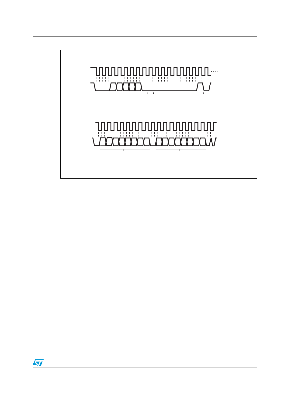
Figure 1. Logic diagram . . . . . . . . . . . . . . . . . . . . . . . . . . . . . . . . . . . . . . . . . . . . . . . . . . . . . . . . . . . . 8
Figure 2. DFN8 and TDFN8 connections (top view) . . . . . . . . . . . . . . . . . . . . . . . . . . . . . . . . . . . . . . 8
Figure 3. Block diagram . . . . . . . . . . . . . . . . . . . . . . . . . . . . . . . . . . . . . . . . . . . . . . . . . . . . . . . . . . . . 9
Figure 4. SMBus/I2C write to pointer register . . . . . . . . . . . . . . . . . . . . . . . . . . . . . . . . . . . . . . . . . . 12
Figure 5. SMBus/I
Figure 6. SMBus/I
Figure 7. SMBus/I
Figure 8. Hysteresis . . . . . . . . . . . . . . . . . . . . . . . . . . . . . . . . . . . . . . . . . . . . . . . . . . . . . . . . . . . . . . 21
Figure 9. Event output boundary timings . . . . . . . . . . . . . . . . . . . . . . . . . . . . . . . . . . . . . . . . . . . . . . 23
Figure 10. Result of setting the write protection. . . . . . . . . . . . . . . . . . . . . . . . . . . . . . . . . . . . . . . . . . 29
Figure 11. Setting the write protection . . . . . . . . . . . . . . . . . . . . . . . . . . . . . . . . . . . . . . . . . . . . . . . . . 30
Figure 12. Write mode sequences in a non write-protected area of SPD . . . . . . . . . . . . . . . . . . . . . . 31
Figure 13. Write cycle polling flowchart using ACK . . . . . . . . . . . . . . . . . . . . . . . . . . . . . . . . . . . . . . . 32
Figure 14. Read mode sequences - SPD . . . . . . . . . . . . . . . . . . . . . . . . . . . . . . . . . . . . . . . . . . . . . . 33
Figure 15. DFN8 – 8-lead dual flat, no-lead (2 mm x 3 mm) package outline (DA) . . . . . . . . . . . . . . . 41
Figure 16. TDFN8 – 8-lead thin dual flat, no-lead (2 mm x 3 mm) package outline (DN) . . . . . . . . . . 42
Figure 17. Carrier tape for DFN8 and TDFN8 packages . . . . . . . . . . . . . . . . . . . . . . . . . . . . . . . . . . . 43
Figure 18. Reel schematic . . . . . . . . . . . . . . . . . . . . . . . . . . . . . . . . . . . . . . . . . . . . . . . . . . . . . . . . . . 44
Figure 19. DA package topside marking information (DFN-8L) . . . . . . . . . . . . . . . . . . . . . . . . . . . . . . 46
Figure 20. DN package topside marking information (TDFN-8L). . . . . . . . . . . . . . . . . . . . . . . . . . . . . 46
Figure 21. Landing pattern - TDFN package (DN) . . . . . . . . . . . . . . . . . . . . . . . . . . . . . . . . . . . . . . . . 47
2
C write to pointer register, followed by a read data word. . . . . . . . . . . . . . . . . . . 12
2
C write to pointer register, followed by a write data word . . . . . . . . . . . . . . . . . . 13
2
C timing diagram . . . . . . . . . . . . . . . . . . . . . . . . . . . . . . . . . . . . . . . . . . . . . . . . . 14
Doc ID 13448 Rev 8 5/50

Description STTS424E02
1 Description
The STTS424E02 is targeted for DIMM modules in mobile personal computing platforms
(laptops), server memory modules and other industrial applications. The thermal sensor
(TS) in the STTS424E02 is compliant with the JEDEC specification JC 42.4, which defines
memory module thermal sensors requirements for mobile platforms. The 2 Kb serial
presence detect (SPD) I
(EEPROM) in the STTS424E02 is organized as 256 x 8 bits and is functionally identical to
the industry standard M34E02.
The TS-SPD EEPROM combination provides space as well as cost savings for mobile and
server platform dual inline memory modules (DIMM) manufacturers, as it is packaged in the
compact 2 mm x 3 mm 8-lead DFN package which is available in two variations. The DA
package has a maximum height of 0.90 mm. The DN package has an identical footprint as
the DA package with a thinner maximum height of 0.80 mm. The DN package is compliant
to JEDEC MO-229, variation WCED-3.
The temperature sensor includes a band gap-based temperature sensor and 10-bit analogto-digital converter (ADC) which monitor and digitize the temperature to a resolution of up to
0.25 °C. The typical accuracies over these temperature ranges are:
±3 °C over the full temperature measurement range of –40 °C to 125 °C,
2
C-compatible electrically erasable programmable memory
±2 °C in the +40 °C to +125 °C temperature range, and
±1 °C in the +75 °C to +95 °C temperature range.
The temperature sensor in the STTS424E02 is specified for operating at supply voltages
from 2.7 V to 3.6 V. Operating at 3.3 V, the supply current is 100 µA (typ) with EEPROM in
standby mode.
The on-board sigma delta ADC converts the measured temperature to a digital value that is
calibrated in °C. For Fahrenheit applications, a lookup table or conversion routine is
required. The STTS424E02 is factory-calibrated and requires no external components to
measure temperature.
The digital temperature sensor component has user-programmable registers that provide
the capabilities for DIMM temperature-sensing applications. The open drain event output pin
is active when the monitoring temperature exceeds a programmable limit, or it falls above or
below an alarm window. The user has the option to set the event output as a critical
temperature output. This pin can be configured to operate in either a comparator mode for
thermostat operation or in interrupt mode.
The 2 Kb serial EEPROM memory in the STTS424E02 has the ability to permanently lock
the data in its first half (upper) 128 bytes (locations 00h to 7Fh). This facility has been
designed specifically for use in DRAM DIMMs with SPD. All of the information concerning
the DRAM module configuration (e.g. access speed, size, and organization) can be kept
write protected in the first half of the memory. The second half (lower) 128 bytes of the
memory can be write protected using two different software write protection mechanisms.
By sending the device a specific sequence, the first 128 bytes of the memory become write
protected: permanently or resettable. In the STTS424E02 the EEPROM write control (WC
is always held low. Thus, the write protection of the memory array is dependent on whether
the software protection has been set.
)
6/50 Doc ID 13448 Rev 8

STTS424E02 Serial communications
2 Serial communications
The STTS424E02 has a simple 2-wire SMBus™/I2C-compatible digital serial interface
which allows the user to access both the 2 Kb serial EEPROM and the data in the
temperature register at any time. It communicates via the serial interface with a master
controller which operates at speeds of up to 400 kHz. It also gives the user easy access to
all of the STTS424E02 registers in order to customize device operation.
2.1 Device type identifier (DTI) code
The JEDEC temperature sensor and EEPROM each have their own unique I2C address,
which ensures that there are no compatibility or data translation issues. This is due to the
fact that each of the devices have their own 4-bit DTI code, while the remaining three bits
are configurable. This enables the EEPROM and thermal sensors to provide their own
individual data via their unique addresses and still not interfere with each others’ operation
in any way. The DTI codes are:
● '0011' for the TS, and
● '1010' for addressing the EEPROM memory array, and
● ‘0110’ to access the software write protection settings of the EEPROM.
Note: The EEPROM in the STTS424E02 package has its WC
(Ground) pad inside the package while the A0, A1, and A2 pins in the logic diagram (see
Figure 1 on page 8) correspond to the chip enable pins E0, E1 and E2 of EEPROM.
pin internally tied to the VSS
Doc ID 13448 Rev 8 7/50
Serial communications STTS424E02
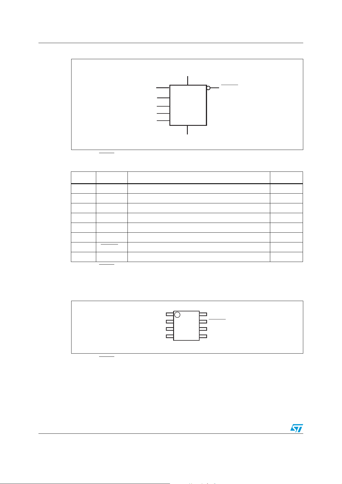
Figure 1. Logic diagram
V
DD
SDA
(1)
EVENT
(1)
SCL
STTS424E02
V
SS
1. SDA and EVENT are open drain.
Table 1. Signal names
A
2
A
1
A
0
Pin Symbol Description Direction
1 A0 Serial bus address selection pin. Can be tied to V
2 A1 Serial bus address selection pin. Can be tied to V
3 A2 Serial bus address selection pin. Can be tied to V
4V
SS
5SDA
Supply ground.
(1)
Serial data. Input/output
or VDD. Input
SS
or VDD. Input
SS
or VDD. Input
SS
6 SCL Serial clock. Input
DD
(1)
Event output pin. Open drain and active-low. Output
Supply power (2.7 V to 3.6 V).
7 EVENT
8V
1. SDA and EVENT are open drain.
AI12261
Note: See Section 2.2: Pin descriptions on page 10 for details.
Figure 2. DFN8 and TDFN8 connections (top view)
A0
A1
A2
GND
1. SDA and EVENT are open drain.
1
2
3
4
8/50 Doc ID 13448 Rev 8
8
7
6
5
V
DD
EVENT
SCL
(1)
SDA
(1)
AI12262
STTS424E02 Serial communications
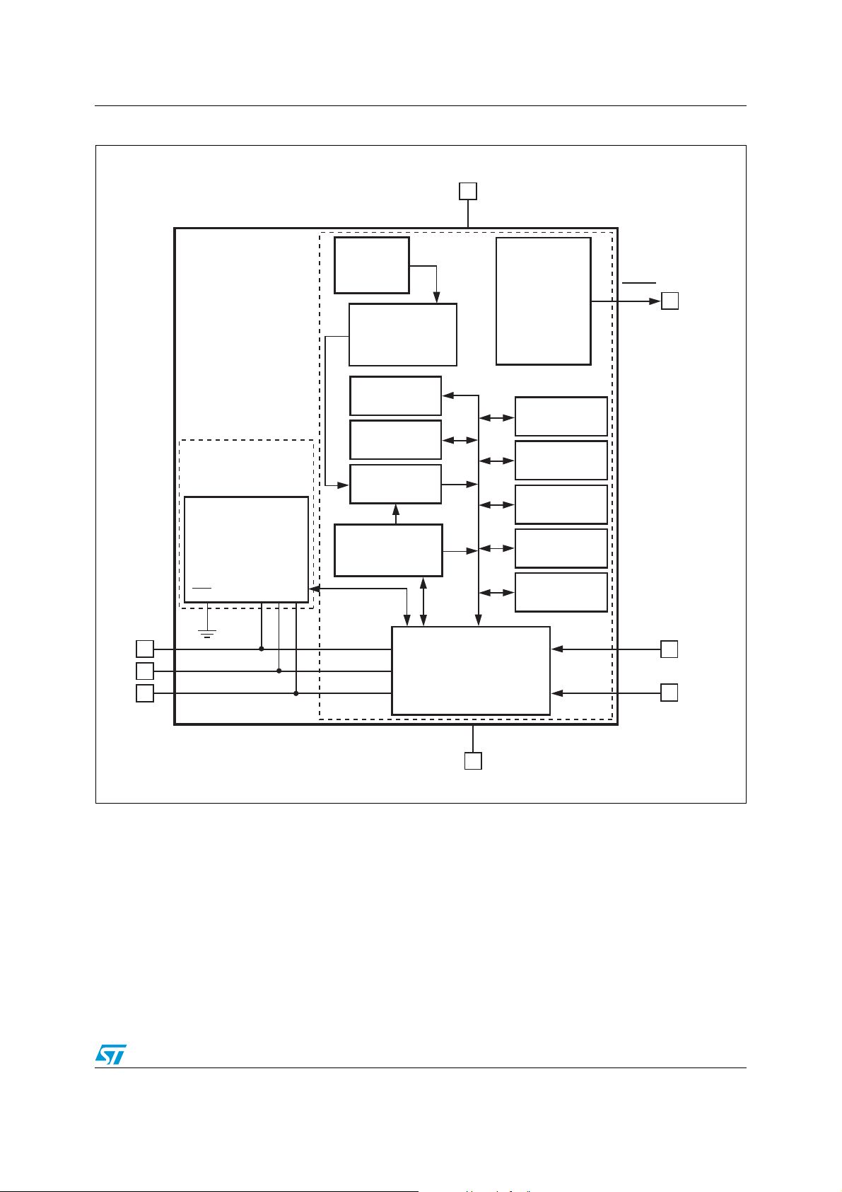
Figure 3. Block diagram
8
V
DD
Temperature
Sensor
EVENT
7
ADC
Capability
Register
Configuration
Register
Temperature
Register
Logic Control
Comparator
Timing
Upper
Register
Lower
Register
Critical
Register
2Kb SPD EEPROM
Software Write Protect
WC E0 E1 E2
V
SS
A0
1
A1
2
A2
3
Address Pointer
Register
SMBus/I2C
Interface
V
SS
4
Manufacturer
ID
Device ID/
Revision
SCL
SDA
6
5
AI12278a
Doc ID 13448 Rev 8 9/50

Serial communications STTS424E02
2.2 Pin descriptions
2.2.1 A0, A1, A2
A2, A1, and A0 are selectable address pins for the 3 LSBs of the I2C interface address.
They can be set to V
internally connected to the E2, E1, E0 (chip selects) of EEPROM.
2.2.2 VSS (ground)
This is the reference for the power supply. It must be connected to system ground.
2.2.3 SDA (open drain)
This is the serial data input/output pin.
2.2.4 SCL
This is the serial clock input pin.
2.2.5 EVENT (open drain)
or GND to provide 8 unique address selections. These pins are
DD
This output pin is open drain and active-low, and functions as an alert interrupt.
2.2.6 VDD (power)
This is the supply voltage pin, and ranges from +2.7 V to +3.6 V.
10/50 Doc ID 13448 Rev 8

STTS424E02 Temperature sensor operation
3 Temperature sensor operation
The temperature sensor continuously monitors the ambient temperature and updates the
temperature data register at least eight times per second. Temperature data is latched
internally by the device and may be read by software from the bus host at any time.
The SMBus/I
same bus. This means that up to 8 memory modules can be supported, given that each
module has one such slave device address slot.
After initial power-on, the configuration registers are set to the default values. The software
can write to the configuration register to set bits per the bit definitions in Section 3.1:
SMBus/I
For details of operation and usage of 2 Kb SPD EEPROM, refer to Section 5: SPD
EEPROM operation.
3.1 SMBus/I2C communications
The registers in this device are selected by the pointer register. At power-up, the pointer
register is set to “00”, which is the capability register location. The pointer register latches
the last location it was set to. Each data register falls into one of three types of user
accessibility:
1. Read-only
2. Write-only, and
3. WRITE/READ same address
2
C slave address selection pins allow up to 8 such devices to co-exist on the
2
C communications.
A WRITE to this device will always include the address byte and the pointer byte. A WRITE
to any register other than the pointer register, requires two data bytes.
Reading this device is achieved in one of two ways:
● If the location latched in the pointer register is correct (most of the time it is expected
that the pointer register will point to one of the read temperature registers because that
will be the data most frequently read), then the READ can simply consist of an address
byte, followed by retrieval of the two data bytes.
● If the pointer register needs to be set, then an address byte, pointer byte, repeat start,
and another address byte will accomplish a READ.
The data byte transfers the MSB first. At the end of a READ, this device can accept either an
acknowledge (ACK) or no acknowledge (NoACK) status from the master. The NoACK status
is typically used as a signal for the slave that the master has read its last byte. This device
subsequently takes up to 125 ms to measure the temperature.
Note: STTS424E02 does not initiate clock stretching which is an optional I
2
C bus feature.
Doc ID 13448 Rev 8 11/50
Temperature sensor operation STTS424E02
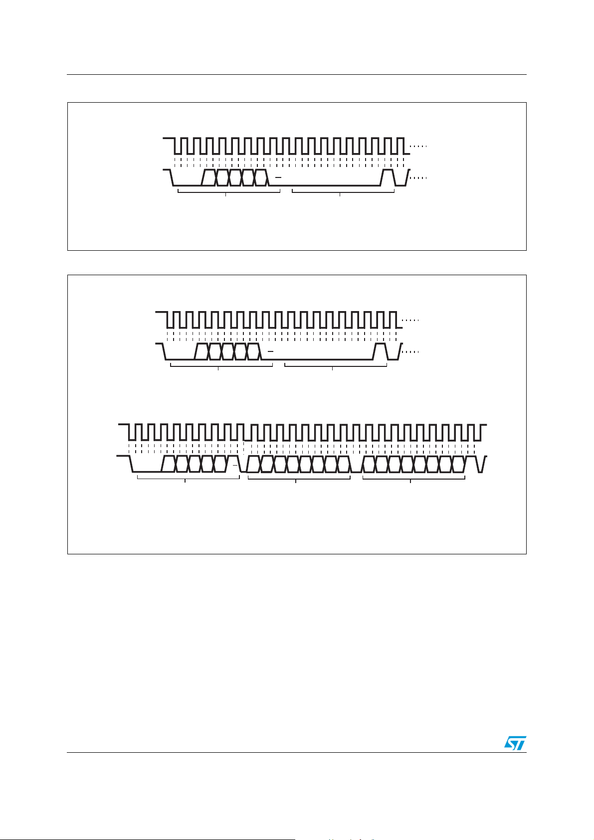
Figure 4. SMBus/I2C write to pointer register
SCL
SDA
Figure 5. SMBus/I
SCL
SDA
Master
SCL
(continued)
19
1199
0
0 1 1 A2 A1 A0 R/W 0 0 0 0 0 D2 D1 D0
Start
by
Master
Address Byte
ACK
by
STTS424E02
2
C write to pointer register, followed by a read data word
1199
0
011A2A1A0R/W 00000D2D1D0
Start
by
Address Byte
ACK
by
STTS424E02
1919
Pointer Byte
Pointer Byte
ACK
by
STTS424E02
ACK
by
STTS424E02
AI12264
SDA
(continued)
Repeat
Start
by
Master
0 0 1 1 A2 A1 A0
Address Byte
R/W
ACK
by
STTS424E02
D14D15
D13
D12
D9D10D11
D7 D6 D5 D4 D3 D2 D1 D0
D8
MSB Data Byte LSB Data Byte
ACK
by
Master
No ACK
by
Master
Stop
Cond.
by
Master
AI12265
12/50 Doc ID 13448 Rev 8
STTS424E02 Temperature sensor operation
Figure 6. SMBus/I2C write to pointer register, followed by a write data word
SCL
SDA
SCL
(continued)
SDA
(continued)
1199
0
011A2A1A0R/W 00000D2D1D0
Start
by
Master
Address Byte
1919
D12
D14D15
D13
MSB Data Byte LSB Data Byte
ACK
by
STTS424E02
D8
D9D10D11
ACK
by
STTS424E02
Pointer Byte
D7 D6 D5 D4 D3 D2 D1 D0
3.2 SMBus/I2C slave sub-address decoding
The physical address for the TS is different than that used by the EEPROM. The TS physical
address is binary 0011A2A1A0RW, where A2, A1, and A0 are the three slave subaddress pins, and the LSB “RW” is the READ/WRITE flag.
ACK
by
STTS424E02
ACK
by
STTS424E02
Stop
Cond.
by
Master
AI14012
The EEPROM physical address is binary 1 010A2A1A0RW for the memory array and is
0110A2A1A0RW for permanently set write protection mode.
Doc ID 13448 Rev 8 13/50
Temperature sensor operation STTS424E02
3.3 SMBus/I2C AC timing consideration
In order for this device to be both SMBus- and I2C-compatible, it complies to a subset of
each specification. The requirements which enable this device to co-exist with devices on
either an SMBus or an I
● The SMBus minimum clock frequency is required.
● The 300 ns SMBus data hold time (THD:DAT) is required (see Figure 7 and Ta bl e 2 o n
page 15.
● The SMBus timeout is maximum 50 ms (temperature sensor only).
2
C bus include:
Note: Since the voltage levels are specified only within 3.3 V ±10%, there are no compatibility
concerns with the SMBus/I
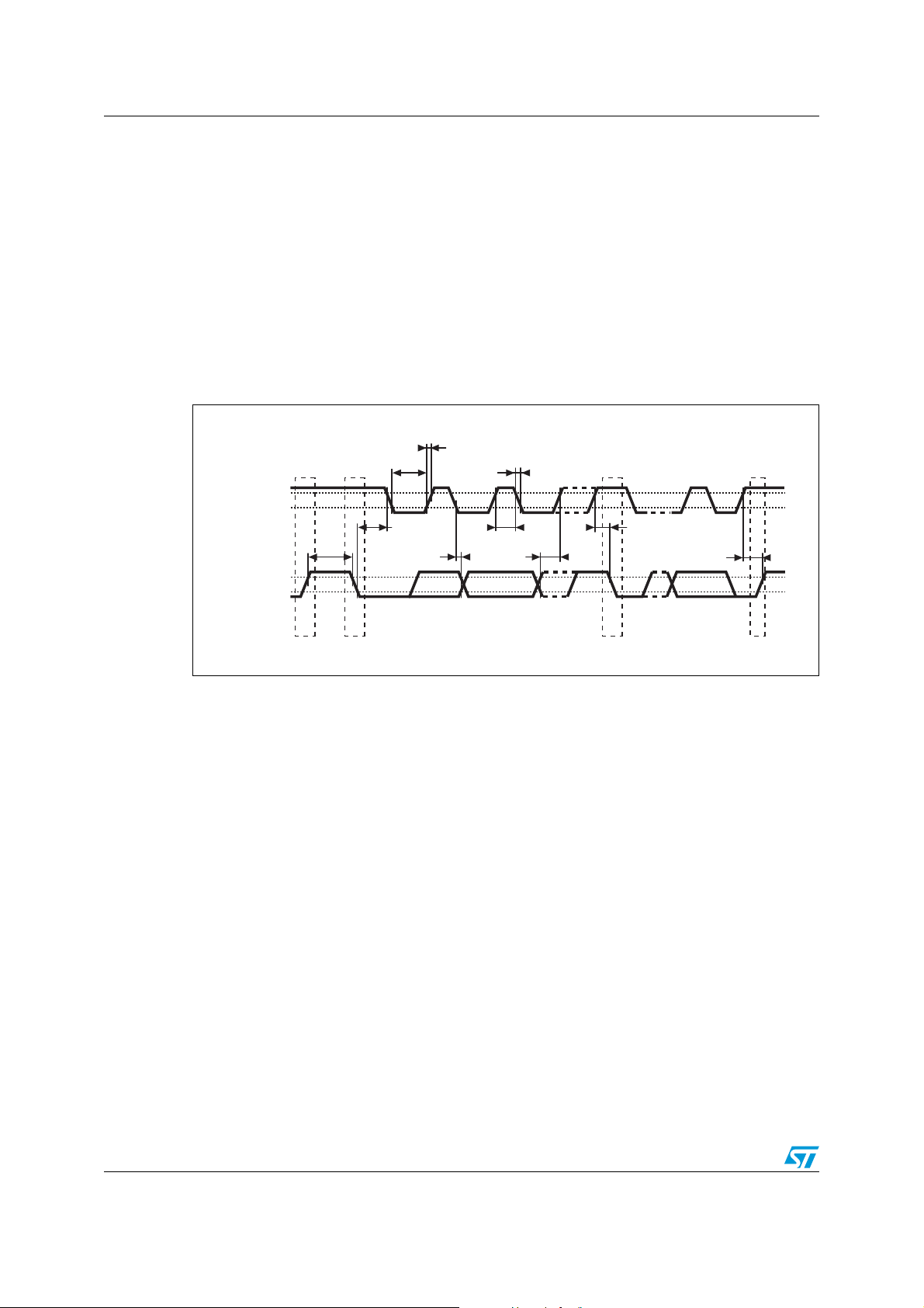
Figure 7. SMBus/I
V
IH
SCL
V
IL
tBUF
V
IH
SDA
V
IL
2
C DC specifications.
2
C timing diagram
tLOW
tHD:STA
tHD:DAT
SP
tR
tF
tHIGH
tSU:DAT
S
tSU:STA
tSU:STO
P
A12266
14/50 Doc ID 13448 Rev 8

STTS424E02 Temperature sensor operation
Table 2. AC SMBus and I2C compatibility timings
Symbol Parameter
t
BUF
t
HD:STA
t
SU:STA
t
HIGH
(2)
t
LOW
t
F
t
R
t
SU:DAT
t
HD:DAT
t
SU:STO
(3)
t
W
f
SCL
t
timeout
1. For a restart condition, or following a WRITE cycle.
2. STTS424E02 will not initiate clock stretching which is an I
3. This parameter reflects maximum WRITE time for EEPROM.
Bus free time between stop (P) and start (S) conditions 4.7 – 1.3 – µs
Hold time after (repeated) start condition. After this
period, the first clock cycle is generated.
(1)
Repeated start condition setup time 4.7 – 0.6 – µs
Clock high period 4.0 – 0.6 – µs
Clock low period 4.7 – 1.3 – µs
Clock/data fall time – 300 – 300 ns
Clock/data rise time – 1000 – 300 ns
Data setup time 250 – 100 – ns
Data hold time 300 – 300 – ns
Stop condition setup time 4.0 – 0.6 – µs
WRITE time for EEPROM – 10 – 10 ms
SMBUS/I2C clock frequency 10 100 10 400 KHz
Bus timeout (temperature sensor only) 25 50 25 50 ms
2
C bus optional feature.
DA package DN package
Units
Min Max Min Max
4.0 – 0.6 – µs
Doc ID 13448 Rev 8 15/50

Temperature sensor registers STTS424E02
4 Temperature sensor registers
The temperature sensor component is comprised of various user-programmable registers.
These registers are required to write their corresponding addresses to the pointer register.
They can be accessed by writing to their respective addresses (see Ta bl e 3 ). Pointer
register bits 7-3 must always be written to '0' (see Ta bl e 4 ). This must be maintained, as not
setting these bits to '0' may keep the device from performing to specifications.
The main registers include:
● Capability register (read-only)
● Configuration register (read/write)
● Temperature register (read-only)
● Temperature trip point registers (R/W), including
– Alarm temperature upper boundary,
– Alarm temperature lower boundary, and
– Critical temperature.
● Manufacturer ID register format
● Device ID and device revision ID register format
See Table 5 on page 17 for pointer register selection bit details.
Table 3. Temperature sensor registers summary
Address (Hex) Register name Power-on default
Not applicable Address pointer Undefined
00 Capability
01 Configuration 0x0000
02 Alarm temperature upper boundary trip 0x0000
03 Alarm temperature lower boundary trip 0x0000
04 Critical temperature trip 0x0000
05 Temperature Undefined
06 Manufacturer’s ID 0x104A
07 Device ID/revision
Table 4. Pointer register format
MSB LSB
C-grade 0x002D
B-grade 0x002F
DA package 0x0000
DN package 0x0001
Bit7 Bit6 Bit5 Bit4 Bit3 Bit2 Bit1 Bit0
0 0 0 0 0 P2 P1 P0
16/50 Doc ID 13448 Rev 8
Pointer/register select bits

STTS424E02 Temperature sensor registers
Table 5. Pointer register select bits (type, width, and default values)
P2 P1 P0 Name Register description
0 0 0 CAPA Thermal sensor capabilities
0 0 1 CONF Configuration 16 R/W
0 1 0 UPPER Alarm temperature upper boundary 16 R/W
0 1 1 LOWER Alarm temperature lower boundary 16 R/W
1 0 0 CRITICAL Critical temperature 16 R/W
1 0 1 TEMP Temperature 16 R 0x0000
1 1 0 MANU Manufacturer ID 16 R 0x104A
1 1 1 ID Device ID/revision
Width
(bits)
C-grade
B-grade 0x002F
DA package
DN package 0x0001
Type
(R/W
16 R
16 R
Default state
)
(POR)
0x002D
0x0000
0x0000
0x0000
0x0000
0x0000
4.1 Capability register (read-only)
This 16-bit register is read-only, and provides the TS capabilities which comply with the
minimum JEDEC JC 42.4 specifications (see Ta bl e 6 and Table 7 on page 18). The
STTS424E02 provides temperatures at 0.25 resolution (10-bit).
4.1.1 Alarm window trip
The device provides a comparison window with an upper temperature trip point in the alarm
upper boundary register, and a lower trip point in the alarm lower boundary register. When
enabled, the event output will be triggered whenever entering or exiting (crossing above or
below) the alarm window.
4.1.2 Critical trip
The device can be programmed in such a way that the event output is only triggered when
the temperature exceeds the critical trip point. The critical temperature setting is
programmed in the critical temperature register. When the temperature sensor reaches the
critical temperature value in this register, the device is automatically placed in comparator
mode, which means that the critical event output cannot be cleared by using software to set
the clear event bit.
Doc ID 13448 Rev 8 17/50

Temperature sensor registers STTS424E02
Table 6. Capability register format
Bit15 Bit14 Bit13 Bit12 Bit11 Bit10 Bit9 Bit8
RFU RFU RFU RFU RFU RFU RFU RFU
Bit7 Bit6 Bit5 Bit4 Bit3 Bit2 Bit1 Bit0
RFU RFU V
Table 7. Capability register bit definitions
HV
TRES1 TRES0
Bit Definition
Basic capability
0
– 0 = Alarm and critical trips turned OFF.
– 1 = Alarm and critical trips turned ON.
Accuracy
– 0 = Accuracy ±2 °C over the active range and ±3 °C over the monitoring range
1
(C-Grade).
– 1 = High accuracy ±1 °C over the active range and ±2 °C over the monitoring range
(B-Grade) (default).
Range width
2
– 0 = Values lower than 0 °C will be clamped and represented as binary value '0'.
– 1 = Temperatures below 0 °C can be read and the Sign bit will be set accordingly.
Temperature resolution
4:3
– 01 = This 10-bit value is fixed for STTS424E02, providing temperatures at 0.25 °C
resolution (LSB).
) High voltage support for A0 (pin 1)
(V
HV
5
– 1 = STTS424E02 supports a voltage up to 10 volts on the A0 pin - (default)
Reserved
15:6
These values must be set to '0'.
Wider
range
Higher
precision
Alarm and
critical trips
18/50 Doc ID 13448 Rev 8

STTS424E02 Temperature sensor registers
4.2 Configuration register (read/write)
The 16-bit configuration register stores various configuration modes that are used to set up
the sensor registers and configure according to application and JEDEC requirements (see
Table 8 on page 19 and Table 9 on page 20).
4.2.1 Event thresholds
All event thresholds use hysteresis as programmed in register address 0x01 (bits 10 through
9) to be set when they de-assert.
4.2.2 Interrupt mode
The interrupt mode allows an event to occur where software may write a '1' to the clear
event bit (bit 5) to de-assert the event interrupt output until the next trigger condition occurs.
4.2.3 Comparator mode
Comparator mode enables the device to be used as a thermostat. READs and WRITEs on
the device registers will not affect the event output in comparator mode. The event signal will
remain asserted until temperature drops outside the range or is re-programmed to make the
current temperature “out of range”.
4.2.4 Shutdown mode
The STTS424E02 features a shutdown mode which disables all power-consuming activities
(e.g. temperature sampling operations), and leaves the serial interface active. This is
selected by setting shutdown bit (bit 8) to '1'. In this mode, the devices consume the
minimum current (I
Note: Bit 8 cannot be set to '1' while bits 6 and 7 (the lock bits) are set to '1'.
The device may be enabled for continuous operation by clearing bit 8 to '0'. In shutdown
mode, all registers may be read or written to. Power recycling will also clear this bit and
return the device to continuous mode as well.
Table 8. Configuration register format
Bit15 Bit14 Bit13 Bit12 Bit11 Bit10 Bit9 Bit8
RFU RFU RFU RFU RFU Hysteresis Hysteresis
Bit7 Bit6 Bit5 Bit4 Bit3 Bit2 Bit1 Bit0
Critical
lock bit
Alarm lock
bit
), as shown in Table 27 on page 38.
SHDN
Clear
event
Event output
status
Event output
control
Critical
event only
Event
polarity
Shutdown
mode
Event
mode
Doc ID 13448 Rev 8 19/50

Temperature sensor registers STTS424E02
Table 9. Configuration register bit definitions
Bit Definition
Event mode
0
– 0 = Comparator output mode (this is the default).
– 1 = Interrupt mode; when either of the lock bits is set, this bit cannot be altered until it is unlocked.
Event polarity
(1)
The event polarity bit controls the active state of the EVENT pin. The EVENT pin is driven to this state
when it is asserted.
1
– 0 = Active-low (this is the default). Requires a pull-up resistor to set the inactive state of the open-
drain output. The power to the pull-up resistor should not be greater than V
state is logical “0”.
– 1 = Active-high. The active state of the pin is then logical “1”.
Critical event only
– 0 = Event output on alarm or critical temperature event (this is the default).
2
– 1 = Event only if the temperature is above the value in the critical temperature register; when the alarm
window lock bit is set, this bit cannot be altered until it is unlocked.
Event output control
3
– 0 = Event output disabled (this is the default).
– 1 = Event output enabled; when either of the lock bits is set, this bit cannot be altered until it is unlocked.
Event status (read-only)
– 0 = Event output condition is not being asserted by this device.
4
(2)
– 1 = Event output condition is being asserted by this device via the alarm window or critical trip event.
Clear event (write-only)
5
– 0 = No effect.
(3)
– 1 = Clears the active event in interrupt mode.
Alarm window lock bit
– 0 = Alarm trips are not locked and can be altered (this is the default).
6
– 1 = Alarm trip register settings cannot be altered. This bit is initially cleared. When set, this bit returns a
logic '1' and remains locked until cleared by an internal power-on reset. These bits can be written to with
a single WRITE, and do not require double WRITEs.
Critical trip lock bit
– 0 = Critical trip is not locked and can be altered (this is the default).
7
– 1 = Critical trip register settings cannot be altered. This bit is initially cleared. When set, this bit returns a
logic '1' and remains locked until cleared by an internal power-on reset. These bits can be written to with
a single WRITE, and do not require double WRITEs.
+ 0.2 V. Active
DD
Shutdown mode
– 0 = TS is enabled (this is the default).
8
– 1 = Shutdown TS when the shutdown, device, and A/D converter are disabled in order to save power. No
event conditions will be asserted; when either of the lock bits is set, this bit cannot be altered until it is
unlocked. However, it can be cleared at any time.
20/50 Doc ID 13448 Rev 8

STTS424E02 Temperature sensor registers
Table 9. Configuration register bit definitions
Bit Definition
Hysteresis enable (see Figure 8 and Ta bl e 1 0)
– 00 = Hysteresis is disabled (this is the default).
– 01 = Hysteresis is enabled at 1.5 °C.
– 10 = Hysteresis is enabled at 3 °C.
10:9
– 11 = Hysteresis is enabled at 6 °C.
Hysteresis applies to all limits when the temperature is dropping below the threshold so that once the
temperature is above a given threshold, it must drop below the threshold minus the hysteresis in order to
be flagged as an interrupt event. Note that hysteresis is also applied to the EVENT
pin functionality. When
either of the lock bits is set, these bits cannot be altered.
Reserved for future use. These bits will always read ‘0’ and writing to them will have no effect. For
15:11
future compatibility, all RFU bits must be programmed as ‘0’.
1. As this device is used in DIMM (memory modules) applications, it is strongly recommended that only the active-low polarity (default) is used.
This is the recommended configuration for the STTS424E02.
2. The actual incident causing the event can be determined from the read temperature register. Interrupt events can be cleared by writing to the
clear event bit (writing to this bit will have no effect on overall device functioning).
3. Writing to this register has no effect on overall device functioning in comparator mode. When read, this bit will always return a logic '0' result.
Figure 8. Hysteresis
T
H
T
L
Below Window bit
Above Window bit
1. TH = Value stored in the alarm temperature upper boundary trip register.
= Value stored in the alarm temperature lower boundary trip register.
2. T
L
3. HYS = Absolute value of selected hysteresis
Table 10. Hysteresis as applied to temperature movement
TH - HYS
Below alarm window bit Above alarm window bit
Temperature slope
Sets Falling T
Clears Rising T
Temperature
threshold
- HYS Rising T
L
L
TL - HYS
Temperature slope
Falling TH - HYS
AI12270
Temperature
threshold
H
Doc ID 13448 Rev 8 21/50

Temperature sensor registers STTS424E02
4.2.5 Event output pin functionality
The event outputs can be programmed to be configured as either a comparator output or as
an interrupt. This is done by enabling the output control bit (bit 3) and setting the event
mode bit (bit 0). The output pin polarity can also be specified as active-high or active-low by
setting the event polarity bit (bit 1).
When the hysteresis bits (bits 10 and 9) are enabled, hysteresis may be used to sense
temperature movement around trigger points. For example, when using the “Above Alarm
window” bit (temperature register bit 14, see Table 12 on page 24) and hysteresis is set to
3 °C, as the temperature rises, bit 14 is set (bit 14 = 1). The temperature is above the alarm
window and the temperature register contains a value that is greater than the value set in
the alarm temperature upper boundary register (see Table 15 on page 25).
If the temperature decreases, bit 14 will remain set until the measured temperature is less
than or equal to the value in the alarm temperature upper boundary register minus 3 °C (see
Figure 8 on page 21 and Table 10 on page 21 for details.
Similarly, when using the “Below Alarm window” bit (temperature register bit 13, see
Table 12 on page 24) will be set to '0'. The temperature is equal to or greater than the value
set in the alarm temperature lower boundary register (see Table 16 on page 25). As the
temperature decreases, bit 13 will be set to '1' when the value in the temperature register is
less than the value in the alarm temperature lower boundary register minus 3 °C (see
Figure 8 on page 21 and Table 10 on page 21 for details.
The device will retain the previous state when entering the shutdown mode. If the device
enters the shutdown mode while the EVENT
due to the additional event output pull-down current.
Note: Hysteresis is also applied to the EVENT
and 7) are set, these bits cannot be altered.
pin is low, the shutdown current will increase
pin functionality. When either of the lock bits (bits 6
22/50 Doc ID 13448 Rev 8

STTS424E02 Temperature sensor registers
Figure 9. Event output boundary timings
T
- T
CRIT
T
UPPER
HYS
- T
T
LOWER
HYS
- T
HYS
T
CRIT
T
UPPER
T
LOWER
Comparator
Interrupt
S/W Int. Clear
Event Output (active-low)
Critical
T
T
A
T
LOWER
- T
HYS
UPPER
- T
HYS
12133574642
Table 11. Legend for Figure 9: Event output boundary timings.
Event output T
Note Event output boundary conditions
Comparator Interrupt Critical 15 14 13
1T
2T
3T
4T
5T
6T
When T
7
the configuration register (interrupt mode) is ignored.
A
≥ T
A
A
< T
≤ T
A
CRIT
≥ T
A
LOWER
LOWER - THYS
> T
A
UPPER
UPPER - THYS
≥ T
A
CRIT
< T
CRIT - THYS
and TA < T
CRIT - THYS
H L H 000
L L H 001
L L H 010
H L H 000
L L L 110
L H H 010
, the event output is in comparator mode and bit 0 of
A
ai12271
bits
Doc ID 13448 Rev 8 23/50

Temperature sensor registers STTS424E02
4.3 Temperature register (read-only)
This 16-bit, read-only register stores the temperature measured by the internal band gap TS
as shown in Ta bl e 1 2 . The STTS424E02 meets the JEDEC mandatory 0.25 °C resolution
requirement. When reading this register, the MSBs (bit 15 to bit 8) are read first, and then
the LSBs (bit 7 to bit 0) are read. The result is the current-sensed temperature. The data
format is 2s complement with one LSB = 0.25 °C. The MSB has a 128 °C resolution.
The trip status bits represent the internal temperature trip detection, and are not affected by
the status of the event or configuration bits (e.g. event output control or clear event). If
neither of the above or below values are set (i.e. both are 0), then the temperature is exactly
within the user-defined alarm window boundaries.
4.3.1 Temperature format
The 16-bit value used in the trip point set and temperature read-back registers is 2s
complement, with the LSB equal to 0.0625 °C (see Tab le 1 3). For example:
1. a value of 019Ch represents 25.75 °C,
2. a value of 07C0h represents 124 °C, and
3. a value of 1E74h represents –24.75 °C
All unused resolution bits are set to zero. The MSB will have a resolution of 128 °C. The
STTS424E02 supports the 0.25 °C/LSB only.
The upper 3 bits indicate trip status based on the current temperature, and are not affected
by the event output status.
Table 12. Temperature register format
Bit
15
Above critical
input
1. See Table 13 for explanation.
Table 13. Temperature register bit definitions
Bit Definition with hysteresis = 0
13
14
15
Sign
MSB
Bit
14
(1)
Below (temperature) alarm window
– 0 = Temperature is equal to or above the alarm window lower boundary temperature.
– 1 = Temperature is below the alarm window.
Above (temperature) alarm window.
– 0 = Temperature is equal to or below the alarm window upper boundary temperature.
– 1 = Temperature is above the alarm window.
Above critical trip
– 0 = Temperature is below the critical temperature setting.
– 1 = Temperature is equal to or above the critical temperature setting.
Above alarm
window
(1)
Bit
13
Below alarm
window
(1)
Bit12Bit 11Bit10Bit9Bit8Bit7Bit6Bit5Bit4Bit3Bit2Bit1Bit
Temperature 0 0
LSB
0
24/50 Doc ID 13448 Rev 8

STTS424E02 Temperature sensor registers
4.4 Temperature trip point registers (R/W)
The STTS424E02 alarm mode registers provide for 11-bit data in 2s compliment format.
The data provides for one LSB = 0.25 °C. All unused bits in these registers are read as '0'.
The STTS424E02 has three temperature trip point registers (see Ta bl e 1 4 ):
● Alarm temperature upper boundary threshold (Tab l e 1 5),
● Alarm temperature lower boundary threshold (Ta bl e 16 ), and
● Critical temperature trip point value (Ta bl e 1 7 ).
Note: If the upper or lower boundary threshold values are being altered in-system, all interrupts
should be turned off until a known state can be obtained to avoid superfluous interrupt
activity.
Table 14. Temperature trip point register format
)
state (POR)
LSB
Default
00 00
00 00
00 00
P2 P1 P0 Name Register description
Width
(bits)
0 1 0 UPPER Alarm temperature upper boundary 16 R/W
0 1 1 LOWER Alarm temperature lower boundary 16 R/W
1 0 0 CRITICAL Critical temperature 16 R/W
Table 15. Alarm temperature upper boundary register format
Sign
MSB
Type
(R/W
Bit15Bit14Bit13Bit12Bit11Bit10Bit9Bit8Bit7Bit6Bit5Bit4Bit3Bit2Bit1Bit
000 Alarm window upper boundary temperature 00
Table 16. Alarm temperature lower boundary register format
Sign
MSB
LSB
Bit15Bit14Bit13Bit12Bit11Bit10Bit9Bit8Bit7Bit6Bit5Bit4Bit3Bit2Bit1Bit
0
0
000 Alarm window lower boundary temperature 00
Table 17. Critical temperature register format
Sign
MSB
LSB
Bit15Bit14Bit13Bit12Bit11Bit10Bit9Bit8Bit7Bit6Bit5Bit4Bit3Bit2Bit1Bit
000 Critical temperature trip point 00
Doc ID 13448 Rev 8 25/50
0

Temperature sensor registers STTS424E02
4.5 Manufacturer ID register (read-only)
The manufacturer’s ID (programmed value 104Ah) in this register is the STMicroelectronics
identification provided by the Peripheral Component Interconnect Special Interest Group
(PCiSIG).
Table 18. Manufacturer ID register format
Bit15 Bit14 Bit13 Bit12 Bit11 Bit10 Bit9 Bit8
00010000
Bit7 Bit6 Bit5 Bit4 Bit3 Bit2 Bit1 Bit0
01001010
4.6 Device ID and device revision ID register (read-only)
The device IDs and device revision IDs are maintained in this register. The register format is
shown in Ta bl e 1 9 . The device IDs and device revision IDs are currently '0' and will be
incremented whenever an update of the device is made.
Table 19. Device ID and device revision ID register format
Bit15 Bit14 Bit13 Bit12 Bit11 Bit10 Bit9 Bit8
00000000
Device ID
Bit7 Bit6 Bit5 Bit4 Bit3 Bit2 Bit1 Bit0
00000000 or 1
Device revision ID
1. DA package, bit0 is 0 (see Table 27 on page 38).
DN package, bit0 is 1 (see Table 27 on page 38).
(1)
26/50 Doc ID 13448 Rev 8

STTS424E02 SPD EEPROM operation
5 SPD EEPROM operation
5.1 2 Kb SPD EEPROM operation
The 2 Kb serial EEPROM is able to lock permanently the data in its first half (from location
00h to 7Fh). This facility has been designed specifically for use in DRAM DIMMs (dual inline
memory modules) with serial presence detect. All the information concerning the DRAM
module configuration (such as its access speed, its size, its organization) can be kept write
protected in the first half of the memory.
The first half of the memory area can be write-protected using two different software write
protection mechanisms. By sending the device a specific sequence, the first 128 bytes of
the memory become write protected: permanently or resetable.
These I
organized as 256x8 bits.
2
I
The device carries a built-in 4-bit device type identifier code (1010) in accordance with the
2
I
(0110) to define the protection. These codes are used together with the voltage level applied
on the three chip enable inputs (A2, A1, A0). These input signals are used to set the value
that is to be looked for on the three least significant bits (b3, b2, b1) of the 7-bit device select
code. In the end application, A0, A1 and A2 must be directly (not through a pull-up or pulldown resistor) connected to V
inputs are not connected, an internal pull-down circuitry makes (A0,A1,A2) = (0,0,0).
2
C-compatible electrically erasable programmable memory (EEPROM) devices are
C uses a two wire serial interface, comprising a bi-directional data line and a clock line.
C bus definition to access the memory area and a second device type identifier code
or VSS to establish the device select code. When these
DD
The A0 input is used to detect the V
voltage, when decoding an SWP or CWP instruction
HV
(refer to Table 20: Device select code).
The device behaves as a slave device in the I
2
C protocol, with all memory operations
synchronized by the serial clock. Read and write operations are initiated by a START
condition, generated by the bus master. The START condition is followed by a device select
code and R/W
bit (as described in Table 20: Device select code), terminated by an
acknowledge bit.
When writing data to the memory, the memory inserts an acknowledge bit during the 9
time, following the bus master’s 8-bit transmission. When data is read by the bus master,
the bus master acknowledges the receipt of the data byte in the same way. Data transfers
are terminated by a STOP condition after an ACK for WRITE, and after a NoACK for READ.
5.2 Internal device reset - SPD EEPROM
In order to prevent inadvertent write operations during power-up, a power on reset (POR)
circuit is included.
At power-up (phase during which V
device will not respond to any instruction until V
threshold voltage (this threshold is lower than the minimum V
Table 2: AC SMBus and I
2
C compatibility timings). Once VDD has passed the POR
threshold, the device is reset.
is lower than VDDmin but increases continuously), the
DD
has reached the power on reset
DD
operating voltage defined in
DD
th
bit
Doc ID 13448 Rev 8 27/50

SPD EEPROM operation STTS424E02
Prior to selecting the memory and issuing instructions, a valid and stable VDD voltage must
be applied. This voltage must remain stable and valid until the end of the transmission of the
instruction and, for a write instruction, until the completion of the internal write cycle (t
At power-down (phase during which V
decreases continuously), as soon as VDD drops
DD
).
W
from the normal operating voltage below the power on reset threshold voltage, the device
stops responding to any instruction sent to it.
Table 20. Device select code
Chip enable
Memory area select code
(two arrays)
Set write protection
(SWP)
Clear write protection
(CWP)
Permanently set write
protection (PSWP)
Read SWP V
Read CWP V
Read PSWP
1. The most significant bit, b7, is sent first.
2. A0, A1 and A2 are compared against the respective external pins on the memory device.
(2)
(2)
(2)
A2A1A01010A2A1A0R/W
V
SSVSSVHV
V
SSVDDVHV
A2 A1 A0 A2 A1 A0 0
SSVSSVHV
SSVDDVHV
A2 A1 A0 A2 A1 A0 1
5.3 Memory addressing
To start communication between the bus master and the slave device, the bus master must
initiate a Start condition. Following this, the bus master sends the device select code, shown
in Table 20: Device select code (on serial data (SDA), most significant bit first).
signals
Device type identifier Chip enable bits R/W
(1)
b7
b6 b5 b4 b3 b2 b1 b0
0010
0110
0110
0011
0111
The device select code consists of a 4-bit device type identifier, and a 3-bit chip enable
“Address” (A2, A1, A0). To address the memory array, the 4-bit device type identifier is
1010b; to access the write-protection settings, it is 0110b.
Up to eight memory devices can be connected on a single I
unique 3-bit code on the chip enable (A0, A1, A2) inputs. When the device select code is
received, the device only responds if the chip enable address is the same as the value on
the chip enable (A0, A1, A2) inputs.
th
The 8
bit is the Read/Write bit (R/W). This bit is set to 1 for read and 0 for write operations.
If a match occurs on the device select code, the corresponding device gives an
acknowledgment on serial data (SDA) during the 9
the device select code, it deselects itself from the bus, and goes into standby mode. The
operating modes are detailed in Tab l e 2 1.
28/50 Doc ID 13448 Rev 8
2
C bus. Each one is given a
th
bit time. If the device does not match

STTS424E02 SPD EEPROM operation
Table 21. Operating modes
Mode R/W bit Bytes Initial sequence
Current address read 1 1 START, device select, R/W
Random address read
0
START, device select, R/W
1
1 reSTART, device select, R/W
= 1
= 0, address
= 1
Sequential read 1 ≥ 1 Similar to current or random address read
Byte write 0 1 START, device select, R/W = 0
Page write 0 ≤ 16 START, device select, R/W
TS write 0 2 START, device select, R/W
TS read 1 2 START, device select, R/W
= 0
= 0, pointer data, stop
= 1, pointer data, stop
Figure 10. Result of setting the write protection
Memory
Area
Standard
Array
Standard
Array
Default EEPROM memory area
state before write access
to the Protect Register
FFh
80h
7Fh
00h
Standard
Array
Write
Protected
Array
State of the EEPROM memory
area after write access
to the Protect Register
FFh
80h
7Fh
00h
AI01936c
5.4 Setting the write protection
The Write Control (WC) is tied low, hence the write protection of the memory array is
dependent on whether software write-protection has been set.
Software write-protection allows the bottom half of the memory area (addresses 00h to 7Fh)
to be write protected irrespective of subsequent states of the write control (WC
Software write-protection is handled by three instructions:
● SWP: Set write protection
● CWP: Clear write protection
● PSWP: Permanently set write protection
The level of write-protection (set or cleared) that has been defined using these instructions,
remains defined even after a power cycle.
Doc ID 13448 Rev 8 29/50
) signal.

SPD EEPROM operation STTS424E02
5.4.1 SWP and CWP
If the software write-protection has been set with the SWP instruction, it can be cleared
again with a CWP instruction.
The two instructions (SWP and CWP) have the same format as a byte write instruction, but
with a different device type identifier (as shown in Tab le 2 0 ). Like the byte write instruction, it
is followed by an address byte and a data byte, but in this case the contents are all “Don’t
Care” (Figure 11). Another difference is that the voltage, V
, must be applied on the A0 pin,
HV
and specific logical levels must be applied on the other two address pins A1 and A2 (as
shown in Ta bl e 2 0 ).
5.4.2 PSWP
If the software write-protection has been set with the PSWP instruction, the first 128 bytes of
the memory are permanently write-protected. This write-protection cannot be cleared by any
instruction, or by power-cycling the device. Also, once the PSWP instruction has been
successfully executed, the SPD EEPROM no longer acknowledges any instruction (with a
device type identifier of 0110) to access the write-protection settings.
Figure 11. Setting the write protection
BUS ACTIVITY
MASTER
SDA LINE
BUS ACTIVITY
5.5 Write operations
Following a start condition the bus master sends a device select code with the R/W bit reset
to 0. The device acknowledges this, as shown in Figure 12, and waits for an address byte.
The device responds to the address byte with an acknowledge bit, and then waits for the
data byte.
When the bus master generates a stop condition immediately after the ACK bit (in the “10
bit” time slot), either at the end of a byte write or a page write, the internal memory write
cycle is triggered. A stop condition at any other time slot does not trigger the internal write
cycle.
During the internal write cycle, serial data (SDA) and serial clock (SCL) are ignored, and the
device does not respond to any requests.
CONTROL
START
BYTE
WORD
ADDRESS
ACK
VAL UE
(DON'T CARE)
DATA
ACK
VAL UE
(DON'T CARE)
ACK
STOP
AI01935b
th
30/50 Doc ID 13448 Rev 8

STTS424E02 SPD EEPROM operation
5.5.1 Byte write
After the device select code and the address byte, the bus master sends one data byte. If
the addressed location is hardware write-protected, the device replies to the data byte with
NoACK, and the location is not modified. If, instead, the addressed location is not writeprotected, the device replies with ACK. The bus master terminates the transfer by
generating a stop condition, as shown in Figure 12.
5.5.2 Page write
The page write mode allows up to 16 bytes to be written in a single write cycle, provided that
they are all located in the same page in the memory: that is, the most significant memory
address bits are the same. If more bytes are sent than will fit up to the end of the page, a
condition known as ‘roll-over’ occurs. This should be avoided, as data starts to become
overwritten in an implementation dependent way.
The bus master sends from 1 to 16 bytes of data, each of which is acknowledged by the
device. After each byte is transferred, the internal byte address counter (the 4 least
significant address bits only) is incremented. The transfer is terminated by the bus master
generating a stop condition.
Figure 12. Write mode sequences in a non write-protected area of SPD
ACK ACK ACK
BYTE WRITE DEV SEL BYTE ADDR DATA IN
START
PAGE WRITE DEV SEL BYTE ADDR DATA IN 1 DATA IN 2
START
ACK ACK
R/W
ACK ACK ACK
R/W
DATA IN N
STOP
STOP
AI01941
Doc ID 13448 Rev 8 31/50

SPD EEPROM operation STTS424E02
5.5.3 Write cycle polling using ACK
During the internal write cycle, the device disconnects itself from the bus, and writes a copy
of the data from its internal latches to the memory cells. The maximum write time (t
shown inTable 2: AC SMBus and I
2
C compatibility timings , but the typical time is shorter. To
make use of this, a polling sequence can be used by the bus master.
The sequence, as shown in Figure 13, is:
● Initial condition: a write cycle is in progress.
● Step 1: the bus master issues a start condition followed by a device select code (the
first byte of the new instruction).
● Step 2: if the device is busy with the internal write cycle, no ACK will be returned and
the bus master goes back to step 1. If the device has terminated the internal write
cycle, it responds with an ACK, indicating that the device is ready to receive the second
part of the instruction (the first byte of this instruction having been sent during step 1).
Figure 13. Write cycle polling flowchart using ACK
WRITE Cycle
in Progress
w
) is
First byte of instruction
with RW = 0 already
decoded by the device
ReSTART
STOP
START Condition
DEVICE SELECT
with RW = 0
ACK
NO
Returned
YES
Next
Operation is
Addressing the
Memory
WRITE Operation
WRITE Operation
YESNO
DATA for the
Continue the
Send Address
and Receive ACK
START
Condition
Random READ Operation
YESNO
DEVICE SELECT
with RW = 1
Continue the
32/50 Doc ID 13448 Rev 8
AI01847c

STTS424E02 SPD EEPROM operation
5.6 Read operations - SPD
Read operations are performed independently of whether hardware or software protection
has been set.
The device has an internal address counter which is incremented each time a byte is read.
Figure 14. Read mode sequences - SPD
CURRENT
ADDRESS
READ
RANDOM
ADDRESS
READ
SEQUENTIAL
CURRENT
READ
SEQUENTIAL
RANDOM
READ
ACK
DEV SEL DATA OUT
R/W
START
ACK
DEV SEL
START
START
DEV SEL
START
(1)
BYTE ADDR
R/W
ACK ACK ACK NO ACK
DEV SEL DATA OUT 1
R/W
ACK ACK
(1)
BYTE ADDR
R/W
NO ACK
ACK
STOP
DEV SEL
START
DEV SEL
START
ACK
(1)
DATA OUT
R/W
DATA OUT N
ACK ACK
(1)
DATA OUT 1
R/W
NO ACK
STOP
STOP
ACK NO ACK
DATA OUT N
1. The seven most significant bits of the device select code of a random read (in the 1st and 3rd bytes) must
be identical.
5.6.1 Random address read - SPD
A dummy write is first performed to load the address into this address counter (as shown in
Figure 14) but without sending a stop condition. Then, the bus master sends another start
condition, and repeats the device select code, with the R/W
acknowledges this, and outputs the contents of the addressed byte. The bus master must
not acknowledge the byte, and terminates the transfer with a stop condition.
Doc ID 13448 Rev 8 33/50
STOP
AI01942
bit set to 1. The device

SPD EEPROM operation STTS424E02
5.6.2 Current address read - SPD
For the current address read operation, following a start condition, the bus master only
sends a device select code with the R/W
bit set to 1. The device acknowledges this, and
outputs the byte addressed by the internal address counter. The counter is then
incremented. The bus master terminates the transfer with a stop condition, as shown in
Figure 14, without acknowledging the byte.
5.6.3 Sequential read - SPD
This operation can be used after a current address read or a random address read. The bus
master does acknowledge the data byte output, and sends additional clock pulses so that
the device continues to output the next byte in sequence. To terminate the stream of bytes,
the bus master must not acknowledge the last byte, and must generate a stop condition, as
shown in Figure 14.
The output data comes from consecutive addresses, with the internal address counter
automatically incremented after each byte output. After the last memory address, the
address counter ‘rolls-over’, and the device continues to output data from memory address
00h.
5.6.4 Acknowledge in read mode
For all read commands, the device waits, after each byte read, for an acknowledgment
during the 9
th
bit time. If the bus master does not drive serial data (SDA) low during this
time, the device terminates the data transfer and switches to its standby mode.
Ta bl e 2 2 and Ta bl e 2 3 show how the ACK bits can be used to identify the write-protection
status.
Table 22. Acknowledge when writing data or defining the write-protection (instructions with
Status
Permanently
protected
Protected with
SWP
Not Protected
R/W
bit=0)
WC
Input
Level
X
0 PSWP ACK
0 PSWP, SWP or CWP ACK
Instruction ACK Address ACK Data byte ACK
PSWP, SWP or CWP NoACK
Page or byte write in
lower 128 bytes
SWP NoACK
CWP ACK
Page or byte write in
lower 128 bytes
Page or byte write ACK Address ACK Data ACK Ye s
Write
cycle(t
Not
significant
ACK Address ACK Data NoACK No
Not
significant
Not
significant
Not
significant
ACK Address ACK Data NoACK No
Not
significant
NoACK
NoACK
ACK
ACK
ACK
Not
significant
Not
significant
Not
significant
Not
significant
Not
significant
NoACK No
NoACK No
ACK Ye s
ACK Ye s
ACK Ye s
)
W
34/50 Doc ID 13448 Rev 8

STTS424E02 SPD EEPROM operation
SWP
PSWP, SWP or CWP NoACK Not significant NoACK Not significant NoACK
SWP NoACK Not significant NoACK Not significant NoACK
CWP ACK Not significant NoACK Not significant NoACK
PSWP ACK Not significant NoACK Not significant NoACK
bit=1)
Table 23. Acknowledge when reading the write protection (instructions with R/W
Status Instruction ACK Address ACK Data byte ACK
Permanently
protected
Protected with
Not protected PSWP, SWP or CWP ACK Not significant NoACK Not significant NoACK
5.7 Initial delivery state - SPD
The device is delivered with all bits in the memory array set to ‘1’ (each byte contains FFh).
Doc ID 13448 Rev 8 35/50

Use in a memory module STTS424E02
6 Use in a memory module
In the dual inline memory module (DIMM) application, the SPD is soldered directly on to the
printed circuit module. The three chip enable inputs (A0, A1, A2) must be connected to V
or V
directly (that is without using a pull-up or pull-down resistor) through the DIMM
DD
socket (see Ta bl e 2 4 ).
SS
The write control (WC
Table 24. DRAM DIMM connections
) of the device is tied to ground to maintain full read and write access.
DIMM position A2 A1 A0
0 V
1 V
2 V
3 V
4 V
5 V
6 V
7 V
6.1 Programming the SPD
The situations in which the SPD EEPROM is programmed can be considered under two
headings:
● when the DIMM is isolated (not inserted on the PCB motherboard)
● when the DIMM is inserted on the PCB motherboard
(0) V
SS
(0) V
SS
(0) V
SS
(0) V
SS
(1) V
DD
(1) V
DD
(1) V
DD
(1) V
DD
(0) V
SS
(0) V
SS
(1) V
DD
(1) VDD(1)
DD
(0) V
SS
(0) V
SS
(1) V
DD
(1) V
DD
SS
DD
SS
SS
DD
SS
DD
(0)
(1)
(0)
(0)
(1)
(0)
(1)
6.1.1 DIMM isolated
With specific programming equipment, it is possible to define the SPD EEPROM content,
using byte and page write instructions, and its write-protection using the SWP and CWP
instructions. To issue the SWP and CWP instructions, the DIMM must be inserted in the
application-specific slot where the A0 signal can be driven to V
instruction. This programming step is mainly intended for use by DIMM makers, whose end
application manufacturers will want to clear this write-protection with the CWP on their own
specific programming equipment, to modify the lower 128 bytes, and finally to set
permanently the write-protection with the PSWP instruction.
6.1.2 DIMM inserted in the application motherboard
As the final application cannot drive the A0 pin to VHV, the only possible action is to freeze
the write-protection with the PSWP instruction.
36/50 Doc ID 13448 Rev 8
during the whole
HV

STTS424E02 Maximum ratings
7 Maximum ratings
Stressing the device above the ratings listed in the absolute maximum ratings table may
cause permanent damage to the device. These are stress ratings only and operation of the
device at these or any other conditions above those indicated in the operating sections of
this specification is not implied. Exposure to absolute maximum rating conditions for
extended periods may affect device reliability.
Table 25. Absolute maximum ratings
Symbol Parameter Value Unit
T
STG
T
SLD
Storage temperature –65 to 150 °C
(1)
Lead solder temperature for 10 seconds 260 °C
A0 VSS – 0.3 to 10.0 V
V
IO
V
DD
I
O
P
D
Input or output voltage
others V
– 0.3 to 6.5 V
SS
Supply voltage VSS – 0.3 to 6.5 V
Output current 10 mA
Power dissipation 320 mW
DA package 128 °C/W
θ
JA
1. Reflow at peak temperature of 260 °C. The time above 255 °C must not exceed 30 seconds.
Thermal resistance
DN package 87.4 °C/W
Doc ID 13448 Rev 8 37/50

DC and AC parameters STTS424E02
8 DC and AC parameters
This section summarizes the operating measurement conditions, and the DC and AC
characteristics of the device. The parameters in the dc and ac characteristics tables that
follow, are derived from tests performed under the measurement conditions summarized in
Ta bl e 2 6 , Operating and AC measurement conditions. Designers should check that the
operating conditions in their circuit match the operating conditions when relying on the
quoted parameters.
Table 26. Operating and AC measurement conditions
V
supply voltage - temperature sensor 2.7 to 3.6 V
DD
Operating temperature –40 to 85 °C
Input rise and fall times ≤ 50 ns
Load capacitance 100 pf
Parameter Conditions Unit
Input pulse voltages 0.2 to 0.8V
Input and output timing reference voltages 0.3 to 0.7V
DD
DD
Table 27. DC/AC characteristics - temperature sensor component with EEPROM
Sym Description Test condition
V
DD
Supply voltage 2.7 3.3 3.6 V
EEPROM active, TS shutdown
F = 400 kHz
I
DD
I
DD1
I
SINK
I
I
ILO
VDD supply current (no load)
supply current,
V
DD
communication only
(no conversions)
TS shutdown mode supply current
EEPROM standby,
SMBUS output low sink current SDA forced to 0.6 V 6 mA
ILI
Input leakage current (SCL, SDA) VIN = VSS or V
Output leakage current
EEPROM (standby)
active temperature conversions
F = 400 kHz
EEPROM
(standby)
TS shutdown
V
= VSS or VDD,
OUT
SDA in Hi-Z
(1)
Min Typ
100 210 µA
100 kHz 40 µA
400 kHz 115 µA
DA package at
85 °C
DN package at
125 °C
DD
1.0 3 µA
1.0 5 µA
(2)
Max Unit
2mA
±4 µA
±4 µA
V
V
38/50 Doc ID 13448 Rev 8

STTS424E02 DC and AC parameters
Table 27. DC/AC characteristics - temperature sensor component with EEPROM (continued)
Sym Description Test condition
falling edge:
V
DD
V
POR
(3)
Power on reset (POR) threshold
DA package
falling edge:
V
DD
DN package
+75 °C < T
C-grade
(4)
2.7 V ≤ V
≤ 3.6 V
DD
+40 °C < T
Accuracy for corresponding range
–40 °C < T
+75 °C < T
B-grade
Accuracy for corresponding range
2.7 V ≤ VDD ≤ 3.6 V
+40 °C < T
–40 °C < T
Resolution 10-bit temperature data
(1)
< +95 ±1.0 ±2.0 °C
A
< +125 ±2.0 ±3.0 °C
A
< +125 ±3.0 ±4.0 °C
A
< +95 ±0.5 ±1.0 °C
A
<+ 125 ±1.0 ±2.0 °C
A
< +125 ±2.0 ±3.0 °C
A
Min Typ
(2)
Max Unit
0.6 V
2.0 V
°C/LS
0.25
10 bits
B
t
CONV
V
OL1
SMBus/I
V
V
C
Conversion time 10-bit 125 ms
Low level voltage
2
C interface
Input logic high SCL, SDA, A0-A2 2.1 V
IH
Input logic low SCL, SDA, A0-A2 0.8 V
IL
SMBus/I2C input capacitance 5 pF
IN
EVENT
IOL = 2.1 mA
;
0.4 V
DA package 10 100 kHz
f
SCL
t
timeout
V
HV
L
AO
V
OL2
Z
AIL
Z
AIH
T
1. Guaranteed operating temperature for DA package: TA = –40 °C to 85 °C and for DN package: TA = –40 °C to 125 °C;
VDD = 2.7 V to 3.6 V (except where noted).
2. Typical numbers taken at V
3. DN is TDFN package max 0.80 mm height.
DA is DFN package max 0.90 mm height.
4. Contact local ST sales office for availability.
SMBus/I2C clock frequency
DN package 10 400 kHz
SMBus timeout 25 50 ms
Allowable voltage on pin A0 10 V
Leakage on pin A0 In overvoltage state 500 µA
Low level voltage SDA IOL = 6 mA 0.6 V
(A0, A1, A2) input impedance VIN < 0.3 V
(A0, A1, A2) input Impedance VIN > 0.7 V
Ambient operating temperature
A
DD
= 3.3 V, TA = 25 °C.
(3)
CC
CC
DA package –40 85 °C
DN package –40 125 °C
30 kΩ
800 kΩ
Doc ID 13448 Rev 8 39/50

Package mechanical data STTS424E02
9 Package mechanical data
In order to meet environmental requirements, ST offers these devices in different grades of
ECOPACK
specifications, grade definitions and product status are available at: www.st.com.
ECOPACK
®
packages, depending on their level of environmental compliance. ECOPACK®
®
is an ST trademark.
40/50 Doc ID 13448 Rev 8

STTS424E02 Package mechanical data
Figure 15. DFN8 – 8-lead dual flat, no-lead (2 mm x 3 mm) package outline (DA)
1. Drawing is not to scale.
Table 28. DFN8 – 8-lead dual flat, no-lead (2 mm x 3 mm) mechanical data (DA)
mm inches
Sym
Min Typ Max Min Typ Max
A 0.80 0.85 0.90 0.031 0.033 0.035
A1 0.00 0.00 0.05 0.000 0.000 0.002
A3 0.20 0.008
b 0.20 0.25 0.30 0.008 0.010 0.012
D 1.95 2.00 2.05 0.077 0.079 0.081
D2 1.35 1.40 1.45 0.053 0.055 0.057
E 2.95 3.00 3.05 0.116 0.118 0.120
E2 1.25 1.30 1.35 0.049 0.051 0.053
e 0.50 0.020
L 0.20 0.30 0.40 0.008 0.012 0.016
ddd 0.08 0.003
7904084_B
Doc ID 13448 Rev 8 41/50

Package mechanical data STTS424E02
Figure 16. TDFN8 – 8-lead thin dual flat, no-lead (2 mm x 3 mm) package outline (DN)
Note: JEDEC MO-229, variation WCED-3 proposal
Table 29. TDFN8 – 8-lead thin dual flat, no-lead (2 mm x 3 mm) mechanical data (DN)
Sym
ddd 0.08 0.003
mm inches
Min Typ Max Min Typ Max
A 0.70 0.75 0.80 0.028 0.030 0.031
A1 0.00 0.00 0.05 0.000 0.000 0.002
A3 0.20 0.008
b 0.20 0.25 0.30 0.008 0.010 0.012
D 1.95 2.00 2.05 0.077 0.079 0.081
D2 1.35 1.40 1.45 0.053 0.055 0.057
E 2.95 3.00 3.05 0.116 0.118 0.120
E2 1.25 1.30 1.35 0.049 0.051 0.053
e 0.50 0.020
L 0.30 0.35 0.40 0.012 0.014 0.016
8089094_A
Note: JEDEC MO-229, variation WCED-3 proposal
42/50 Doc ID 13448 Rev 8

STTS424E02 Package mechanical data
Figure 17. Carrier tape for DFN8 and TDFN8 packages
P
D
T
A
TOP COVER
TAPE
K
0
0
CENTER LINES
OF CAVITY
P
2
B
0
0
P
1
E
F
W
USER DIRECTION OF FEED
Table 30. Carrier tape dimensions for DFN8 and TDFN8 packages
Package W D E P
DFN8
TDFN8
8.00
+0.30
–0.10
8.00
+0.30
–0.10
1.50
+0.10/
–0.00
1.50
+0.10/
–0.00
1.75
±0.10
1.75
±0.10
4.00
±0.10
4.00
±0.10
P
0
2.00
±0.10
2.00
±0.10
FA0B
2
3.50
±0.05
3.50
±0.05
2.30
±0.10
2.30
±0.10
0
2.80
±0.10
3.20
±0.10
K
0
1.10
±0.01
1.10
±0.10
P
1
4.00
±0.10
4.00
±0.10
AM03073v1
TUnit
0.30
0.30
mm 3000
mm 3000
±0.05
±0.05
Bulk
Qty
Doc ID 13448 Rev 8 43/50

Package mechanical data STTS424E02
Figure 18. Reel schematic
T
40mm min.
Access hole
At slot location
B
D
C
A
Tape slot
Full ra dius
In core for
Tape s tart
2.5mm min.width
N
G measured
At hub
Table 31. Reel dimensions for 8 mm carrier tape - TDFN8 and DFN8 packages
A
(max)
180 mm
(7-inch)
B
(min)
1.5 mm
C
13 mm
± 0.2 mm
D
(min)
N
(min)
20.2 mm 60 mm
G
8.4 mm
+ 2/–0 mm
The dimensions given in Tab l e 3 1 incorporate tolerances that cover all variations on critical
parameters.
AM04928v1
T
(max)
14.4 mm
44/50 Doc ID 13448 Rev 8

STTS424E02 Part numbering
10 Part numbering
Table 32. Ordering information scheme
Example: STTS424E02 B DN 3 F
Device type
STTS424E02
Grade
B: Maximum accuracy 75 °C to 95 °C = ± 1 °C
C: Maximum accuracy 75 °C to 95 °C = ±2 °C
Package
DN = TDFN8 (0.80 mm max height)
DA = DFN8 (0.90 mm max height)
(1)
(2)
(3)
(4)
Tem peratur e
3 = –40 °C to 125 °C (DN package only)
6 = –40 °C to 85 °C (DA package only)
Shipping method
®
F = ECOPACK
1. Not recommended for new design (refer to the STTS2002 as drop-in replacement). Contact ST sales office
for availability.
2. Contact local ST sales office for availability.
3. DN package is only available in B accuracy grade and in temperature grade 3.
4. DA package available only in temperature grade 6.
package, tape & reel packing
For other options, or for more information on any aspect of this device, please contact the
ST sales office nearest you.
Doc ID 13448 Rev 8 45/50

Package marking information STTS424E02
11 Package marking information
Figure 19. DA package topside marking information (DFN-8L)
(1)
E42X
(2)
xxxx
ai13907
1. Option codes:
X = B or C accuracy grade. For example, E42C is C-grade.
2. Traceability codes
Note: Contact local ST sales office for availability.
Figure 20. DN package topside marking information (TDFN-8L)
(1)
E42X
(2)
xxxx
(3)
xxxx
1. Option codes:
X = B or C accuracy grade. For example, E42C is C-grade.
2. Package/fab code identifier
3. Traceability codes
ai13907b
46/50 Doc ID 13448 Rev 8

STTS424E02 Landing pattern
12 Landing pattern
The landing pattern recommendations per the JEDEC proposal for the TDFN package (DN)
are shown in Figure 21.
The preferred implementation with wide corner pads enhances device centering during
assembly, but a narrower option is defined for modules with tight routing requirements.
Figure 21. Landing pattern - TDFN package (DN)
e4
e2
e/2
e
L
e/2
E3
E3
K
D2
D2/2
K
L
b2
b4
K2
b
K2
D2/2
b
K2
E2/2
E2
E2/2
ai14000
Doc ID 13448 Rev 8 47/50

Landing pattern STTS424E02
Ta bl e 3 3 lists variations of landing pattern implementations, ranked as “Preferred” and
“Minimum Acceptable” based on the JEDEC proposal.
Table 33. Parameters for landing pattern - TDFN package (DN)
Dimension
Parameter Description
Min Nom Max
D2 Heat paddle width 1.40 - 1.60
E2 Heat paddle height 1.40 - 1.60
E3 Heat paddle centerline to contact inner locus 1.00 - -
L Contact length 0.70 - 0.80
K Heat paddle to contact keepout 0.20 - -
K2 Contact to contact keepout 0.20 - -
e Contact centerline to contact centerline pitch for inner contacts - 0.50 -
b Contact width for inner contacts 0.25 - 0.30
e2
b2 Corner contact width, “minimum acceptable option”
e4
b4 Corner contact width, “preferred” option
1. Minimum acceptable option to be used when routing prevents preferred width contact.
2. Preferred option to be used when possible.
Landing pattern centerline to outer contact centerline, “minimum
acceptable” option
Landing pattern centerline to outer contact centerline, “preferred”
(2)
option
(1)
(1)
(2)
-0.50-
0.25 - 0.30
-0.60-
0.45 - 0.50
48/50 Doc ID 13448 Rev 8

STTS424E02 Revision history
13 Revision history
Table 34. Document revision history
Date Revision Changes
13-Apr-2007 1 Initial release.
09-May-2007 2 Updated Ta bl e 3 , 5, 6, 7, 27, 28 and 32.
04-Jun-2007 3 Updated Ta b le 2 7 .
02-Jul-2007 4 Added POR threshold values to Tab l e 2 7 , updated Tab le 2 8 .
Added TDFN package (cover page, Figure 16, Tab le 2 9 ) and landing
18-Mar-2008 5
12-Jun-2008 6
08-Oct-2009 7
12-Oct-2010 8
pattern recommendations (Figure 21, Ta b l e 33 ); updated Section 1, 2,
Ta bl e 2 , 3, 5, 6, 7, 11, 19, 25, 27, 28, 29, 32, Figure 2, 15, 19, 20).
Updated cover page, Figure 4, 5, 8, 14; Section 4.3.1,Section 5.4.1;
Ta bl e 5 , 11, 25, 27, 32; added Figure 6; removed TSSOP8 package
throughout datasheet.
Reformatted document; added tape and reel specifications (Figure 17,
Ta bl e 3 0 ); updated Features, text in Section 1, Section 3.1, Section 3.3,
Section 5.3, Section 5.4.2, Section 5.5.2, Section 5.5.3, Section 9;
updated Figure 5, 16, 19, 20, Ta bl e 2 , 7, 9, 11, 13, 21, 25, 26, 27, 29, 32.
Device is not recommended for new design; updated document status,
cover page, Tab l e 3 2 , Figure 19, 20; added Figure 18, Ta bl e 3 1 .
Doc ID 13448 Rev 8 49/50

STTS424E02
Please Read Carefully:
Information in this document is provided solely in connection with ST products. STMicroelectronics NV and its subsidiaries (“ST”) reserve the
right to make changes, corrections, modifications or improvements, to this document, and the products and services described herein at any
time, without notice.
All ST products are sold pursuant to ST’s terms and conditions of sale.
Purchasers are solely responsible for the choice, selection and use of the ST products and services described herein, and ST assumes no
liability whatsoever relating to the choice, selection or use of the ST products and services described herein.
No license, express or implied, by estoppel or otherwise, to any intellectual property rights is granted under this document. If any part of this
document refers to any third party products or services it shall not be deemed a license grant by ST for the use of such third party products
or services, or any intellectual property contained therein or considered as a warranty covering the use in any manner whatsoever of such
third party products or services or any intellectual property contained therein.
UNLESS OTHERWISE SET FORTH IN ST’S TERMS AND CONDITIONS OF SALE ST DISCLAIMS ANY EXPRESS OR IMPLIED
WARRANTY WITH RESPECT TO THE USE AND/OR SALE OF ST PRODUCTS INCLUDING WITHOUT LIMITATION IMPLIED
WARRANTIES OF MERCHANTABILITY, FITNESS FOR A PARTICULAR PURPOSE (AND THEIR EQUIVALENTS UNDER THE LAWS
OF ANY JURISDICTION), OR INFRINGEMENT OF ANY PATENT, COPYRIGHT OR OTHER INTELLECTUAL PROPERTY RIGHT.
UNLESS EXPRESSLY APPROVED IN WRITING BY AN AUTHORIZED ST REPRESENTATIVE, ST PRODUCTS ARE NOT
RECOMMENDED, AUTHORIZED OR WARRANTED FOR USE IN MILITARY, AIR CRAFT, SPACE, LIFE SAVING, OR LIFE SUSTAINING
APPLICATIONS, NOR IN PRODUCTS OR SYSTEMS WHERE FAILURE OR MALFUNCTION MAY RESULT IN PERSONAL INJURY,
DEATH, OR SEVERE PROPERTY OR ENVIRONMENTAL DAMAGE. ST PRODUCTS WHICH ARE NOT SPECIFIED AS "AUTOMOTIVE
GRADE" MAY ONLY BE USED IN AUTOMOTIVE APPLICATIONS AT USER’S OWN RISK.
Resale of ST products with provisions different from the statements and/or technical features set forth in this document shall immediately void
any warranty granted by ST for the ST product or service described herein and shall not create or extend in any manner whatsoever, any
liability of ST.
ST and the ST logo are trademarks or registered trademarks of ST in various countries.
Information in this document supersedes and replaces all information previously supplied.
The ST logo is a registered trademark of STMicroelectronics. All other names are the property of their respective owners.
© 2010 STMicroelectronics - All rights reserved
STMicroelectronics group of companies
Australia - Belgium - Brazil - Canada - China - Czech Republic - Finland - France - Germany - Hong Kong - India - Israel - Italy - Japan -
Malaysia - Malta - Morocco - Philippines - Singapore - Spain - Sweden - Switzerland - United Kingdom - United States of America
www.st.com
50/50 Doc ID 13448 Rev 8
 Loading...