0.5 A max constant current LED driver
Features
■ Up to 40 V input voltage
■ Less than 0.5 V voltage overhead
■ Up to 0.5 A output current
■ PWM dimming pin
■ Shutdown pin
■ LED disconnection diagnostic
■ Slope control with external cap
Applications
■ LED constant current supplying for varying
input voltages
■ Low voltage lighting
■ Small appliances LED lighting
■ Car LED lights
Description
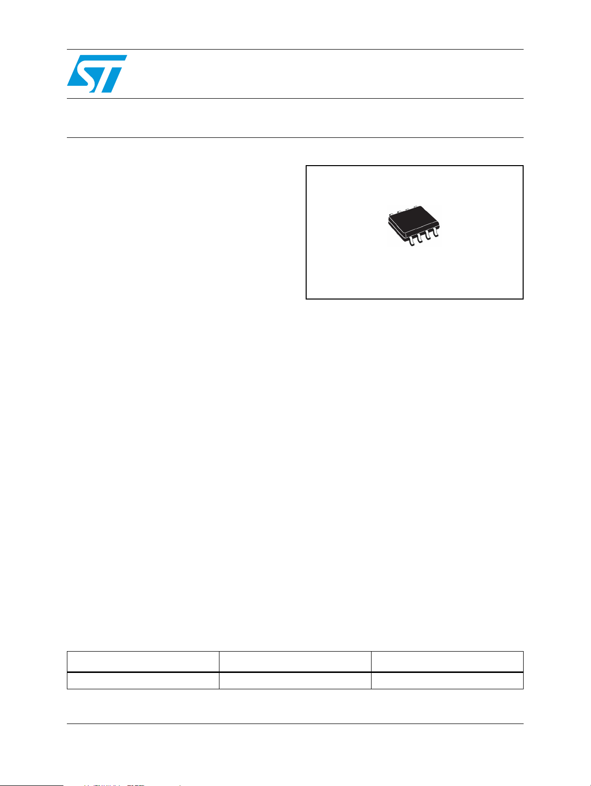
The STCS05A is a BiCMOS constant current
source designed to provide a precise constant
current starting from a varying input voltage
source. The main target is to replace discrete
STCS05A
SO-8
components solution for driving LEDs in low
voltage applications such as 5 V, 12 V or 24 V
giving benefits in terms of precision, integration
and reliability.
The current is set with external resistor up to 0.5
A with a ± 10 % precision; a dedicated pin allows
implementing PWM dimming. An external
capacitor allows setting the slope for the current
rise from tens of microseconds to tens of
milliseconds allowing reduction of EMI.
An open-drain pin output provides information on
load disconnection condition.
Table 1. Device summary
Order code Package Packaging
STCS05ADR SO-8 2500 parts per reel
July 2008 Rev 2 1/18
www.st.com
18

Contents STCS05A
Contents
1 Application diagram . . . . . . . . . . . . . . . . . . . . . . . . . . . . . . . . . . . . . . . . . 3
2 Pin configuration . . . . . . . . . . . . . . . . . . . . . . . . . . . . . . . . . . . . . . . . . . . 4
3 Maximum ratings . . . . . . . . . . . . . . . . . . . . . . . . . . . . . . . . . . . . . . . . . . . . 5
4 Electrical characteristics . . . . . . . . . . . . . . . . . . . . . . . . . . . . . . . . . . . . . 6
5 Timing . . . . . . . . . . . . . . . . . . . . . . . . . . . . . . . . . . . . . . . . . . . . . . . . . . . . . 7
6 Typical performance characteristics . . . . . . . . . . . . . . . . . . . . . . . . . . . . 8
7 Detail description . . . . . . . . . . . . . . . . . . . . . . . . . . . . . . . . . . . . . . . . . . 10
7.1 Current setting . . . . . . . . . . . . . . . . . . . . . . . . . . . . . . . . . . . . . . . . . . . . . 10
7.2 Enable . . . . . . . . . . . . . . . . . . . . . . . . . . . . . . . . . . . . . . . . . . . . . . . . . . . 10
7.3 PWM dimming . . . . . . . . . . . . . . . . . . . . . . . . . . . . . . . . . . . . . . . . . . . . . 10
7.4 Diagnostic . . . . . . . . . . . . . . . . . . . . . . . . . . . . . . . . . . . . . . . . . . . . . . . . . 11
8 Application information . . . . . . . . . . . . . . . . . . . . . . . . . . . . . . . . . . . . . 12
8.1 Reverse polarity protection . . . . . . . . . . . . . . . . . . . . . . . . . . . . . . . . . . . . 12
8.2 Thermal considerations . . . . . . . . . . . . . . . . . . . . . . . . . . . . . . . . . . . . . . 12
9 Package mechanical data . . . . . . . . . . . . . . . . . . . . . . . . . . . . . . . . . . . . 14
10 Revision history . . . . . . . . . . . . . . . . . . . . . . . . . . . . . . . . . . . . . . . . . . . 17
2/18
STCS05A Application diagram
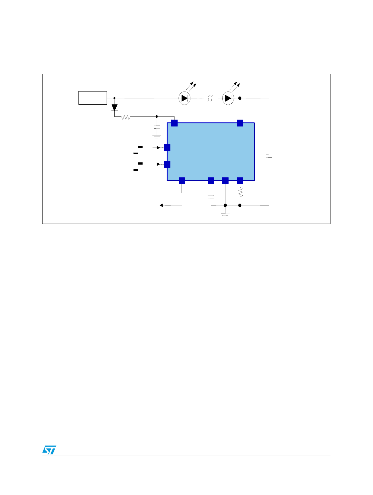
1 Application diagram
Figure 1. Typical application diagram for 0.5 A LED current
V
V
IN
IN
4.5V to 40V
4.5V to 40V
BAT46ZFILM
BAT46ZFILM
RIN100 ohm
RIN100 ohm
OFF
OFF
OFF
OFF
C
C
BYP
BYP
0.1µF
0.1µF
ON
ON
ON
ON
Load disconnection
Load disconnection
(Open Drain output)
(Open Drain output)
V
V
PWM
PWM
EN
EN
CC
CC
DISC
DISC
STCS05A
STCS05A
C
C
SLOPE
SLOPE
10nF
10nF
DRAIN
DRAIN
C
C
DRAIN
DRAIN
0.47µF
0.47µF
FB
FB
GNDSLOPE
GNDSLOPE
R
R
FB
FB
0.2 ohm
0.2 ohm
3/18
Pin configuration STCS05A
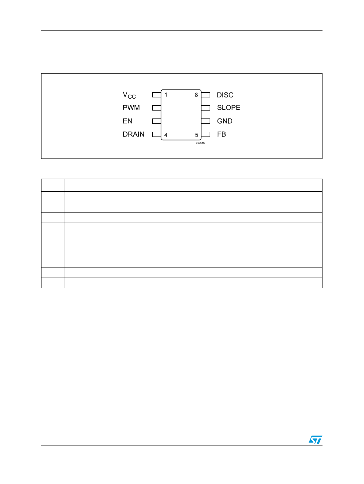
2 Pin configuration
Figure 2. Pin connections (top view)
Table 2. Pin description
Pin n° Symbol Note
1V
2 PWM PWM dimming input
3 EN Shutdown pin
4 DRAIN Internal N-MOSFET drain
5FB
6 GND Ground
7 SLOPE Capacitor for slope control
8 DISC Load disconnection flag (open drain)
CC
Supply voltage
Feedback input. The control loop regulates the current in such a way that the average
voltage at the FB input is 100 mV (nominal). The cathode of the LED and a resistor to
ground to set the LED current should be connected at this point.
4/18
STCS05A Maximum ratings
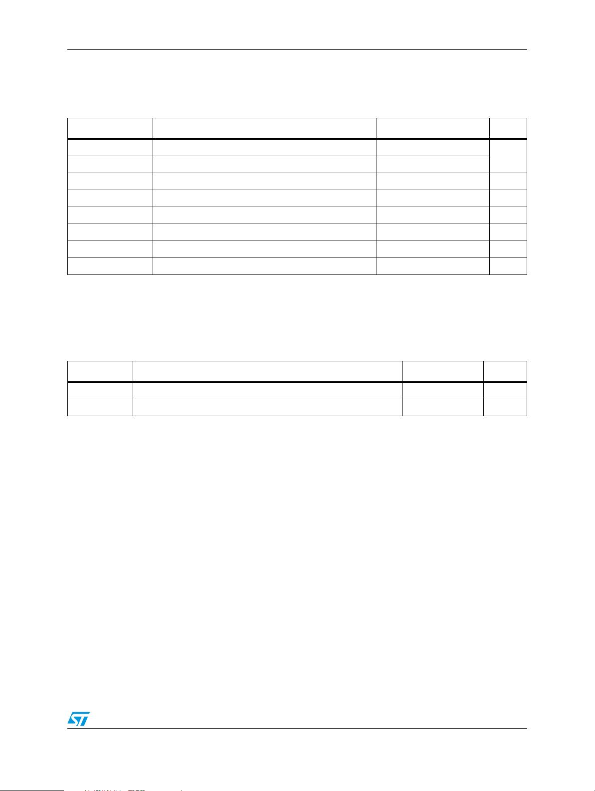
3 Maximum ratings
Table 3. Absolute maximum ratings
Symbol Parameter Value Unit
V
CC
DC supply voltage -0.3 to +45
V
DRAIN Drain pin -0.3 to +45
PWM, EN, DISC Logic pins -0.3 to + V
+ 0.3 V
CC
SLOPE, FB Configuration pins -0.3 to + 3.3 V
ESD Human body model (all pins) ±2 kV
(1)
Power Dissipation SO-8 T
T
J
T
STG
1. See Figure 16 for details of max power dissipation for ambient temperature higher than 25 °C
Junction temperature -40 to 150 °C
Storage temperature range -55 to 150 °C
=25°C
A
0.85 W
Note: Absolute maximum ratings are those values beyond which damage to the device may occur.
Functional operation under these conditions is not implied.
Table 4. Thermal data
Symbol Parameter SO-8 Unit
R
thJC
R
thJA
1. This value depends from thermal design of PCB on which the device is mounted.
Thermal resistance junction-case 20 °C/W
Thermal resistance junction-ambient
(1)
100 °C/W
5/18
Electrical characteristics STCS05A
4 Electrical characteristics
Table 5. Electrical characteristics (V
C
DRAIN
= 1 µF; C
= 100 nF typical values are at TA = 25 °C, unless otherwise specified)
BYP
= 12 V; IO = 100 mA; TJ = -40 °C to 125 °C; V
CC
DRAIN
Symbol Parameter Test conditions Min. Typ. Max. Unit
V
CC
Supply voltage range 4.5 40 V
Output current range 1 500 mA
I
O
Output current R
Regulation (percentage with
respect to V
V
FB
Feedback Voltage IO = 0 to 0.5A 90 100 110 mV
CC
= 12 V)
= 0.2 Ω 500 mA
FB
V
= 4.5 to 40V,
CC
IO = 100mA; V
DRAIN
= 1V
-1 +1 %
On Mode 450 750
V
LEAK
TR/T
DISC
I
CC
DROP
DRAIN
T
D
Quiescent current (Measured on
VCC pin)
Dropout voltage (V
DRAIN
to GND)
Drain leakage current Shutdown; V
Rise/Fall time of the current on
F
PWM transition
Delay on PWM signal (see
Figure 3)
Low level voltage I
Leakage current V
Load disconnection threshold
DRAIN
-GND)
(V
Shutdown Mode;
= 5 to 12V
V
CC
Shutdown Mode;
V
= 12 to 40V
CC
I
= 100mA 0.12 0.16
O
= 0.5A 0.58 0.9
I
O
= 40V 10 µA
DRAIN
C
T
V
C
V
C
= 10 nF,
SLOPE
= -40 °C to 105 °C
J
rising, V
PWM
= floating,
SLOPE
falling, V
PWM
= floating
SLOPE
= 5mA 0.2 0.5 V
SINK
= 5V 1 µA
DISC
CC
CC
= 12V
= 12V
800 µs
3
1.2
DISC Turn-ON 75
DISC Turn-OFF 110
1
3
= 1 V;
µA
V
µs
mV
Thermal
Protection
Shutdown temperature 155
°C
Hysteresis 25
Logic inputs (PWM and EN)
V
V
Input low level 0.4 V
L
Input high level 1.2 V
H
EN, PWM leakage current V
PWM input leakage current V
= 5V; V
EN
= 40V 60
EN
= 40V 120
PWM
= 5V 2
PWM
µAEN input leakage current V
Note: All devices 100 % production tested at TA = 25 °C. Limits over the operating temperature
range are guaranteed by design.
6/18

STCS05A Timing
5 Timing
Figure 3. PWM and output current timing
PWM
PWM
90%
90%
10%
Current
Current
10%
Trise
Trise
T
T
D
D
Tfall
Tfall
T
T
D
D
Figure 4. Block diagram
High Voltage
High Voltage
45 V
45 V
Preregulator
V
V
CC
CC
EN
EN
PWM
PWMPWM
GND
GNDGND
Preregulator
3.3 V
3.3 V
Enable
Enable
Input
Input
PWM
PWM
Input
Input
Bandgap
Bandgap
Bandgap
1.23 V
1.23 V
1.23 V
Enable,
Enable,
PWM &
PWM &
Slope controll
Slope controll
Logic
Logic
SLOPE
SLOPE
Shutdown
Shutdown
all blocks
all blocks
Slope
Slope
Control
Control
100 mV
100 mV100 mV
75 mV
75 mV
Low Voltage 3.3 V
Low Voltage 3.3 V
Thermal
Thermal
Thermal
Shutdown
Shutdown
Shutdown
+
+-+
-
-
Comp
Comp
+
+-+
-
-
Logic
Logic
Disc
Disc
comp
comp
Driver
Driver
H.V.
H.V.
45 V
45 V
DISC
DISC
DRAIN
DRAIN
FB
FB
7/18

Typical performance characteristics STCS05A
6 Typical performance characteristics
Figure 5. I
Figure 7. I
vs VCC, TA = 25 °C Figure 6. I
DRAIN
vs temperature Figure 8. V
DRAIN
vs R
DRAIN
1000
1000
100
100
[mA]
[mA]
DRAIN
DRAIN
I
I
10
10
1
1
0.1 1 10 100
0.1 1 10 100
DROP
SET
RFB[Ω]
RFB[Ω]
(including VFB) vs
temperature
Figure 9. ICC vs temperature Figure 10. ICC vs V
8/18
CC

STCS05A Typical performance characteristics
Figure 11. T
Figure 13. Rise time Figure 14. Fall time
I
DRAIN
rise/Tfall
= 80 mA - C
vs C
= 10nF - TA = 25° C
SLOPE
SLOPE
Figure 12. Turn-on time
I
= 80 mA - C
DRAIN
I
= 80 mA - C
DRAIN
= 10nF - TA = 25° C
SLOPE
= 10nF - TA = 25° C
SLOPE
V
2V/DIV
PWM
I
20mA/DIV
DRAIN
V
1V/DIV
DRAIN
Time 210µsec/DIV
V
2V/DIV
PWM
20mA/DIV
I
DRAIN
V
1V/DIV
DRAIN
Time 200µsec/DIV
V
2V/DIV
PWM
I
20mA/DIV
DRAIN
V
1V/DIV
DRAIN
Time 200µsec/DIV
9/18

Detail description STCS05A
7 Detail description
The STCS05A is a BiCMOS constant current source designed to provide a precise constant
current starting from a varying input voltage source. The main target is to replace discrete
components solution for driving LEDs in low voltage applications such as 5 V, 12 V or 24 V
giving benefits in terms of precision, integration and reliability.
7.1 Current setting
The current is set with an external sensing resistor connected to the FB pin. The feedback
voltage is 100 mV, then a low resistor value can be chosen reducing power dissipation. A
value between 1 mA and 500 mA can be set according to the resistor value, the resulting
output current has a tolerance of ± 10 %.
For instance, should one need a 350 mA LEDs current, R
the following equation:
R
= V
FB
/ I
F
= 100 mV / 350 mA = 284 mΩ
LEDs
7.2 Enable
When the enable pin is low the device completely off thus reducing current consumption to
less than 1 µA. When in shutdown mode, the internal main switch is off.
7.3 PWM dimming
The PWM input allows implementing PWM dimming on the LED current; when the PWM
input is high the main switch will be on and vice versa. A typical frequency range for the
input is from few Hertz to 50 kHz. The maximum dimming frequency is limited by the
minimum rise/fall time of the current (obtained with C
Above 50 kHz the current waveforms starts assuming a triangular shape.
While the PWM input is switching, the overall circuitry remains on, this is needed in order to
implement two important features: short delay time and controlled slope for the current.
Since the PWM pin is controlling just the main switch, the overall circuitry is always on and it
is able to control the delay time between the PWM input signal and the output current in the
range of few µs, this is important to implement synchronization among several light LED
sources.
should be selected according to
F
= 0) which is around 4 µs each.
SLOPE
10/18
The rise and fall slope of the current is controlled by the C
time are linear dependent from the C
characteristics). A controlled rise time has two main benefits: reducing EMI noise and avoid
current spike at turn on.
When C
condition an overshoot can be present on the LED current before the system goes into
regulation.
is left floating, the internal switch is turned on at maximum speed, in this
SLOPE
capacitor value (see graph in typical
SLOPE
capacitor. The rise and fall
SLOPE

STCS05A Detail description
7.4 Diagnostic
When STCS05A is in on mode (EN is high), the device is able to detect disconnection or fail
of the LED string monitoring V
pulled low regardless the PWM pin status. This information can be used by the system to
inform that some problem happens in the LEDs.
DRAIN
pin. If V
is lower than 75 mV the DISC pin is
DRAIN
11/18

Application information STCS05A
8 Application information
8.1 Reverse polarity protection
STCS05A must be protected from reverse connection of the supply voltage. Since the
current sunk from V
to protect the chip. Care must be taken for the whole application circuit, especially for the
LEDs, in fact, in case a negative voltage is applied between V
voltage will be applied to the LED string that must have a total breakdown voltage higher
than the negative applied voltage in order to avoid any damage.
Figure 15. Reverse polarity condition
V
V
V
V
pin is in the range of 450 µA a small diode connected to VCC is able
CC
and GND, a negative
IN
IN
IN
IN
IN
BAT46
BAT46
or similar
or similar
or similar
or similar
V
V
V
V
CC
CC
CC
CC
DRAIN
DRAIN
DRAIN
DRAIN
+
+
+
+
8.2 Thermal considerations
The STCS05A is able to control a LED current up to 500 mA and able to sustain a voltage
on the drain pin up to 40 V. Those operating conditions are however limited by thermal
constraints, the thermal resistances shown in the thermal data section is the typical ones.
The power dissipation in the device can be calculated as follow:
P
= (V
D
basing on this and on the thermal resistance and ambient temperature, the junction
temperature can be calculated as:
T
= R
J
A typical application could be:
– Input voltage: 12 V;
– 3 white LEDs with an typical V
– LEDs current: 350 mA;
–Package: SO-8;
–T
DRAIN
x PD + T
thJA
= 50 °C;
A
- VFB) x I
A
LED
+ (V
CC
x ICC)
F
PWM
PWM
PWM
PWM
EN
EN
EN
EN
DISC
DISC
DISC
DISC
= 3.6 V;
FB
FB
FB
FB
GNDSLOPE
GNDSLOPE
GNDSLOPE
GNDSLOPE
12/18

STCS05A Application information
In this case V
P
= (1.2 - 0.1) x 0.35 + 12 x 0.5 x 10-3 = 0.385 + 6 x 10-3 = 391 mW
D
= 12 - 3 x 3.6 = 1.2 V
DRAIN
The junction temperature will be:
T
= 100 x 0.391 + 50 = 89 °C
J
For a correct operation of the chip, the junction temperature must not exceed 110 °C.
The following pictures show the maximum power dissipation according to the ambient
temperature:
Figure 16. Maximum power dissipation vs T
1.40
1.40
1.20
1.20
1.00
1.00
[W]
[W]
0.80
0.80
DMAX
DMAX
0.60
0.60
P
P
0.40
0.40
0.20
0.20
P
= (T
P
= (T
DMAX
DMAX
25 35 45 55 65 75 85 95 105 115 125
25 35 45 55 65 75 85 95 105 115 125
JMAX-TA
JMAX-TA
for SO-8
A
)/R
)/R
thJA
thJA
[°C]
[°C]
R
R
thJA
thJA
= 100 [°C/W]
= 100 [°C/W]
13/18

Package mechanical data STCS05A
9 Package mechanical data
In order to meet environmental requirements, ST offers these devices in ECOPACK®
packages. These packages have a lead-free second level interconnect. The category of
second Level Interconnect is marked on the package and on the inner box label, in
compliance with JEDEC Standard JESD97. The maximum ratings related to soldering
conditions are also marked on the inner box label. ECOPACK is an ST trademark.
ECOPACK specifications are available at: www.st.com.
14/18

STCS05A Package mechanical data
SO-8 mechanical data
Dim.
A1.35 1.75 0.053 0.069
A1 0.10 0.25 0.04 0.010
A2 1.10 1.65 0.043 0.065
B0.33 0.51 0.013 0.020
C0.19 0.25 0.007 0.010
D4.80 5.00 0.189 0.197
E 3.80 4.00 0.150 0.157
e 1.27 0.050
H5.80 6.20 0.228 0.244
h 0.25 0.50 0.010 0.020
L 0.40 1.27 0.016 0.050
k 8° (max.)
ddd 0.1 0.04
Min. Typ. Max. Min. Typ. Max.
mm. inch.
0016023/C
15/18

Package mechanical data STCS05A
Tape & reel SO-8 mechanical data
mm. inch.
Dim.
Min. Typ. Max. Min. Typ. Max.
A 330 12.992
C 12.8 13.2 0.504 0.519
D 20.2 0.795
N60 2.362
T 22.4 0.882
Ao 8.1 8.5 0.319 0.335
Bo 5.5 5.9 0.216 0.232
Ko 2.1 2.3 0.082 0.090
Po 3.9 4.1 0.153 0.161
P7.98.1 0.311 0.319
16/18

STCS05A Revision history
10 Revision history
Table 6. Document revision history
Date Revision Changes
04-Mar-2008 1 Initial release.
02-Jul-2008 2 Modified: Table 5 on page 6.
17/18

STCS05A
Please Read Carefully:
Information in this document is provided solely in connection with ST products. STMicroelectronics NV and its subsidiaries (“ST”) reserve the
right to make changes, corrections, modifications or improvements, to this document, and the products and services described herein at any
time, without notice.
All ST products are sold pursuant to ST’s terms and conditions of sale.
Purchasers are solely responsible for the choice, selection and use of the ST products and services described herein, and ST assumes no
liability whatsoever relating to the choice, selection or use of the ST products and services described herein.
No license, express or implied, by estoppel or otherwise, to any intellectual property rights is granted under this document. If any part of this
document refers to any third party products or services it shall not be deemed a license grant by ST for the use of such third party products
or services, or any intellectual property contained therein or considered as a warranty covering the use in any manner whatsoever of such
third party products or services or any intellectual property contained therein.
UNLESS OTHERWISE SET FORTH IN ST’S TERMS AND CONDITIONS OF SALE ST DISCLAIMS ANY EXPRESS OR IMPLIED
WARRANTY WITH RESPECT TO THE USE AND/OR SALE OF ST PRODUCTS INCLUDING WITHOUT LIMITATION IMPLIED
WARRANTIES OF MERCHANTABILITY, FITNESS FOR A PARTICULAR PURPOSE (AND THEIR EQUIVALENTS UNDER THE LAWS
OF ANY JURISDICTION), OR INFRINGEMENT OF ANY PATENT, COPYRIGHT OR OTHER INTELLECTUAL PROPERTY RIGHT.
UNLESS EXPRESSLY APPROVED IN WRITING BY AN AUTHORIZED ST REPRESENTATIVE, ST PRODUCTS ARE NOT
RECOMMENDED, AUTHORIZED OR WARRANTED FOR USE IN MILITARY, AIR CRAFT, SPACE, LIFE SAVING, OR LIFE SUSTAINING
APPLICATIONS, NOR IN PRODUCTS OR SYSTEMS WHERE FAILURE OR MALFUNCTION MAY RESULT IN PERSONAL INJURY,
DEATH, OR SEVERE PROPERTY OR ENVIRONMENTAL DAMAGE. ST PRODUCTS WHICH ARE NOT SPECIFIED AS "AUTOMOTIVE
GRADE" MAY ONLY BE USED IN AUTOMOTIVE APPLICATIONS AT USER’S OWN RISK.
Resale of ST products with provisions different from the statements and/or technical features set forth in this document shall immediately void
any warranty granted by ST for the ST product or service described herein and shall not create or extend in any manner whatsoever, any
liability of ST.
ST and the ST logo are trademarks or registered trademarks of ST in various countries.
Information in this document supersedes and replaces all information previously supplied.
The ST logo is a registered trademark of STMicroelectronics. All other names are the property of their respective owners.
© 2008 STMicroelectronics - All rights reserved
STMicroelectronics group of companies
Australia - Belgium - Brazil - Canada - China - Czech Republic - Finland - France - Germany - Hong Kong - India - Israel - Italy - Japan -
Malaysia - Malta - Morocco - Singapore - Spain - Sweden - Switzerland - United Kingdom - United States of America
www.st.com
18/18
 Loading...