

Page 1
High power buck-boost white LED driver
Features
■ Buck-boost DC-DC converter
■ Drives one power LED up to 1 A in flash mode
■ Drives one power LED up to 800 mA in
continuous mode
■ LED temperature protection
■ Output current control
■ 1.8 MHz (typ.) fixed frequency PWM
■ Synchronous rectification
■ High efficiency across the total input voltage
range
■ Operational modes:
– Shutdown mode
– High current mode: up to 1 A
– Low current mode: from 20 mA
■ Adjustable current in both modes
■ Peak inductor limited to 2.3 A (typ.)
■ LED disconnected from the battery in
shutdown mode
■ NTC LED temperature protection
■ Overvoltage protection: 5.3 V
■ Short-circuit protection
■ Overtemperature protection
■ ULVLO function
■ 1 µA max shutdown current
■ QFN16 (4 x 4 x 1 mm) 16 leads
Applications
STCF07
QFN16 (4 x 4 mm)
Description
The STCF07 is a dedicated, size-optimized
solution for driving a power LED. The device is a
buck-boost converter which guarantees proper
LED current control over all possible battery
voltage and LED forward voltage conditions. The
output current control ensures good current
regulation over the forward voltage spread
characteristics of high-brightness LEDs. The
device includes various functions to protect the
chip and the power LEDs. These include soft-start
control as well as detection and protection of chip
overtemperature and shorted LEDs. An optional
external NTC is supported to protect the LEDs
against overheating. It is possible to separately
program the current intensity in HIGH and LOW
mode using the SEL pin. The device is housed in
a 16-lead QFN16 (4 x 4 mm) package with a
height less than 1 mm.
■ Camera flash for mobile phones
■ Power supply for high power LEDs
Table 1. Device summary
Order code Package Packaging
STCF07PNR QFN16 (4 x 4 mm) Tape and reel
April 2011 Doc ID 16757 Rev 2 1/26
www.st.com
26
Page 2

Contents STCF07
Contents
1 Block diagram . . . . . . . . . . . . . . . . . . . . . . . . . . . . . . . . . . . . . . . . . . . . . . 4
2 Pin configuration . . . . . . . . . . . . . . . . . . . . . . . . . . . . . . . . . . . . . . . . . . . . 5
3 Maximum ratings . . . . . . . . . . . . . . . . . . . . . . . . . . . . . . . . . . . . . . . . . . . . 6
4 Application information . . . . . . . . . . . . . . . . . . . . . . . . . . . . . . . . . . . . . . 7
5 Electrical characteristics . . . . . . . . . . . . . . . . . . . . . . . . . . . . . . . . . . . . . 8
6 Introduction . . . . . . . . . . . . . . . . . . . . . . . . . . . . . . . . . . . . . . . . . . . . . . . 10
7 Logic pin description . . . . . . . . . . . . . . . . . . . . . . . . . . . . . . . . . . . . . . . 11
7.1 CSEL pin . . . . . . . . . . . . . . . . . . . . . . . . . . . . . . . . . . . . . . . . . . . . . . . . . 11
7.2 FAULT pin . . . . . . . . . . . . . . . . . . . . . . . . . . . . . . . . . . . . . . . . . . . . . . . . . 11
7.3 ENABLE pin . . . . . . . . . . . . . . . . . . . . . . . . . . . . . . . . . . . . . . . . . . . . . . . 11
8 Detailed description . . . . . . . . . . . . . . . . . . . . . . . . . . . . . . . . . . . . . . . . 12
8.1 Buck-boost converter . . . . . . . . . . . . . . . . . . . . . . . . . . . . . . . . . . . . . . . . 12
8.2 High current mode . . . . . . . . . . . . . . . . . . . . . . . . . . . . . . . . . . . . . . . . . . 12
8.3 Low current mode . . . . . . . . . . . . . . . . . . . . . . . . . . . . . . . . . . . . . . . . . . . 12
8.4 Shutdown mode . . . . . . . . . . . . . . . . . . . . . . . . . . . . . . . . . . . . . . . . . . . . 12
8.5 Soft-start . . . . . . . . . . . . . . . . . . . . . . . . . . . . . . . . . . . . . . . . . . . . . . . . . . 12
8.6 STCF07 protection features . . . . . . . . . . . . . . . . . . . . . . . . . . . . . . . . . . . 13
8.6.1 Peak current and short-circuit protection . . . . . . . . . . . . . . . . . . . . . . . . 13
8.6.2 Overvoltage protection . . . . . . . . . . . . . . . . . . . . . . . . . . . . . . . . . . . . . . 13
8.6.3 Thermal shutdown protection . . . . . . . . . . . . . . . . . . . . . . . . . . . . . . . . 13
8.6.4 Sensing of LED temperature with the NTC resistor . . . . . . . . . . . . . . . . 13
8.6.5 Undervoltage lockout function . . . . . . . . . . . . . . . . . . . . . . . . . . . . . . . . 14
9 PCB design . . . . . . . . . . . . . . . . . . . . . . . . . . . . . . . . . . . . . . . . . . . . . . . 15
9.1 PCB design rules . . . . . . . . . . . . . . . . . . . . . . . . . . . . . . . . . . . . . . . . . . . 15
9.2 PCB design of the demonstration board . . . . . . . . . . . . . . . . . . . . . . . . . 16
9.3 Schematic of the demonstration board . . . . . . . . . . . . . . . . . . . . . . . . . . . 18
2/26 Doc ID 16757 Rev 2
Page 3

STCF07 Contents
10 Typical performance characteristics . . . . . . . . . . . . . . . . . . . . . . . . . . . 19
11 External component selection . . . . . . . . . . . . . . . . . . . . . . . . . . . . . . . . 20
11.1 Input and output capacitor selection . . . . . . . . . . . . . . . . . . . . . . . . . . . . . 20
11.2 Inductor selection . . . . . . . . . . . . . . . . . . . . . . . . . . . . . . . . . . . . . . . . . . . 20
11.3 LED selection . . . . . . . . . . . . . . . . . . . . . . . . . . . . . . . . . . . . . . . . . . . . . . 20
11.4 RHC selection . . . . . . . . . . . . . . . . . . . . . . . . . . . . . . . . . . . . . . . . . . . . . 20
11.5 RLC selection . . . . . . . . . . . . . . . . . . . . . . . . . . . . . . . . . . . . . . . . . . . . . . 21
11.6 NTC and RX resistor selection . . . . . . . . . . . . . . . . . . . . . . . . . . . . . . . . . 21
12 Package mechanical data . . . . . . . . . . . . . . . . . . . . . . . . . . . . . . . . . . . . 22
13 Revision history . . . . . . . . . . . . . . . . . . . . . . . . . . . . . . . . . . . . . . . . . . . 25
Doc ID 16757 Rev 2 3/26
Page 4
Block diagram STCF07
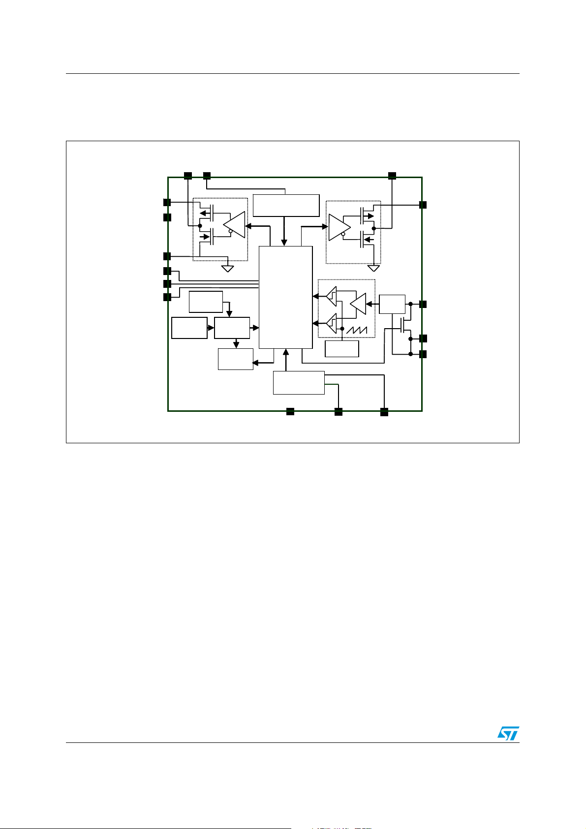
1 Block diagram
Figure 1. STCF07 block diagram
VLX2VLX1AVLX1B
VLX2VLX1AVLX1B
CURRENT
PVBAT
PVBAT
VBAT
VBAT
GND
GND
ENABLE
ENABLE
CSEL
CSEL
FAULT
FAULT
OVER
OVER
TEMP
TEMP
CURRENT
PROTECTION
PROTECTION
LOGIC
LOGIC
MX
MX
VOUT
VOUT
FB1
FB1
BANDGAP
BANDGAP
REF
REF
SOFT
SOFT
START
START
REF
REF
DRIVER
DRIVER
OSC
OSC
NTC
NTC
CONTROL
CONTROL
PNGD RX NTC
PNGD RX NTC
FB2
FB2
FB2S
FB2S
4/26 Doc ID 16757 Rev 2
Page 5
STCF07 Pin configuration
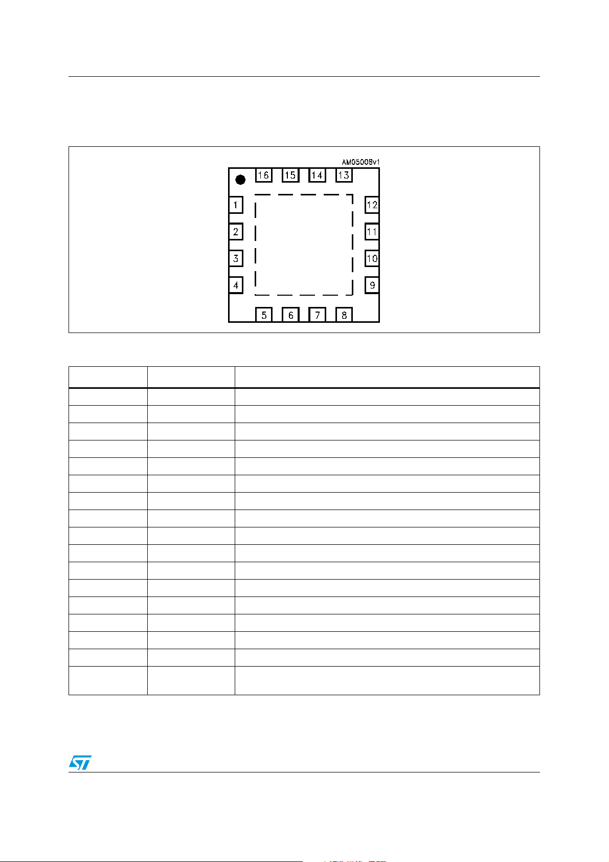
2 Pin configuration
Figure 2. STCF07 pin connections (top view)
Table 2. STCF07 pin description
Pin n° Symbol Description
1 VLX2 Inductor VLX2 connection
8RXR
resistor connection
X
2 NTC NTC resistor connection
3 VOUT Output voltage
4 FB1 Feedback pin [I
5FB2R
bypass
TR
6 FB2S Feedback pin [I
*(RHC+RLC)]
LED
LED*RHC
]
14 GND Signal ground
13 CSEL Current selection
7 EN Enable
16 FAULT Diagnostic
9 PVBAT Power supply voltage
10 VBAT Supply voltage
11 VLX1A Inductor VLX1 connection
12 VLX1B Inductor VLX1 connection
15 PGND Power ground
Exposed pad PGND
To be connected to the PCB ground plane for optimal electrical and
thermal performance
Doc ID 16757 Rev 2 5/26
Page 6
Maximum ratings STCF07
3 Maximum ratings
Table 3. Absolute maximum ratings
Symbol Parameter Value Unit
VBAT Signal supply voltage -0.3 to 6 V
PVBAT Power supply voltage -0.3 to 6 V
VLX1A, VLX1B Inductor connection 1 -0.3 to V
VLX2 Inductor connection 2 -0.3 to V
+0.3 V
I
+0.3 V
I
VOUT Output voltage -0.3 to 6 V
FB1, FB2, FB2S Feedback and sense voltage -0.3 to 3 V
R
X
CSEL Current selection -0.3 to V
EN Enable -0.3 to V
FAULT Diagnostic -0.3 to V
Connection for reference resistor -0.3 to 3 V
+0.3 V
I
+0.3 V
I
+0.3 V
I
NTC Connection for LED temperature sensing -0.3 to 3 V
ESD Human body model ±2kV
P
T
T
STG
TOT
OP
T
J
Continuous power dissipation (at TA = 70 °C) 800 mW
Operating junction temperature range -40 to 85 °C
Junction temperature -40 to 150 °C
Storage temperature range -65 to 150 °C
Note: Absolute maximum ratings are those values beyond which damage to the device may occur.
Functional operation under these condition is not implied.
Table 4. Thermal data
Symbol Parameter Value Unit
(1)
R
thJA
1. Junction-to-ambient thermal resistance in JEDEC still air chamber. Thermal test board JESD51-7 (leaded surface mount
packages).
6/26 Doc ID 16757 Rev 2
Thermal resistance junction-ambient 31 °C/W
Page 7
STCF07 Application information
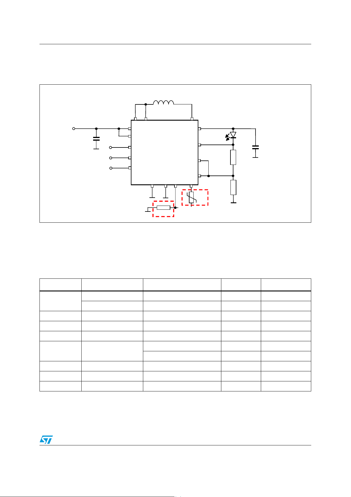
4 Application information
Figure 3. Application schematic diagram
L
L
V
V
IN
IN
C
C
IN
IN
VLX1 VLX1
VLX1 VLX1
PVBAT
PVBAT
VBAT
VBAT
ENABLE
ENABLE
CSEL
CSEL
FAULT
FAULT
GND PGND
GND PGND
RX
RX
VLX2
VLX2
VOUT
VOUT
FB1
FB1
FB2
FB2
FB2S
FB2S
NTC
NTC
NTC
NTC
LED
LED
R
R
LC
LC
R
R
HC
HC
C
C
OUT
OUT
R
R
X
X
Optional components
Optional components
Note: Represents a typical application schematic for an output current of 800 mA (max) in
continuous mode operation. For pulse/flash mode operation it is possible to increase the
maximum output current up to 1 A. If the battery voltage is higher than 3.1 V, the chip is
capable of delivering the maximum output current of up to 1 A in continuos mode.
Table 5. List of external components
Component Manufacturer Part number Value Size
C
NTC MURATA NCP18WF104J03RB 100 kΩ 0805
1. For 800 mA output current performance.
2. For 1000 mA output current performance.
Welwyn LR1206-R20FI
R
R
C
HC
LC
IN
OUT
KOA SR732BTTDR160F
Tyco Electronics CRL1220T1R8J 1.8 Ω 0805
TDK C1608X5R0J106MT 10 µF 0603
TDK C1608X5R0J475M 4.7 µF 0603
VLF4014ST-2R2M1R9
LTDK
VLF5014S-2R2M2R3
R
X
Tyco Electronics 1-1879132-9 15 kΩ 0402
LED Luxeon LXHL_PW09
(1)
(2)
(2)
(1)
0.2 Ω 1206
0.16 Ω 1206
2.2 µH / 1.4 A 3.5x3.8x1.4 mm
2.2 µH / 2.3 A 4.6x4.8x1.4 mm
Note: The above-listed external components refer to a typical application. Operation of the
STCF07 is not limited to the use of these components.
Doc ID 16757 Rev 2 7/26
Page 8
Electrical characteristics STCF07
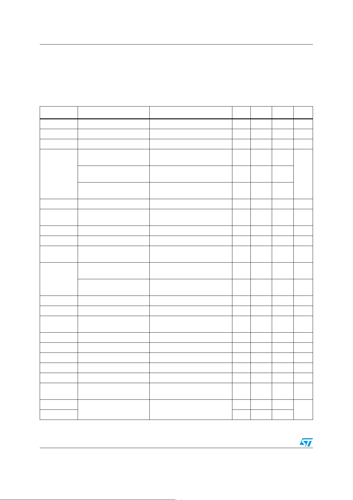
5 Electrical characteristics
TA = 25 °C, VI = 3.6 V, 2 x CI = 10 µF, CO = 1 µF, L = 2.2 µH, RHC = 0.22 Ω, RLC = 1.8 Ω,
R
= 15 kΩ
X
Table 6. Electrical characteristics
Symbol Parameter Test conditions Min. Typ. Max. Unit
V
I
UVLO Undervoltage lockout V
V
PW_ONRESET
I
O
V
OUT
ILIM Inductor peak current
Input voltage supply 2.7 5.5 V
= 2.7 V 2.2 V
I
Power ON reset threshold VI rising 2.3 V
Output current - high current
level
Output current - high current
level
Output current - low current
level
CSEL = VI; VI = 2.7 V to 5.5 V;
R
= 0.16 Ω, P
HC
CSEL = V
R
HC
; VI = 3.2 V to 5.5 V;
I
= 0.16 Ω, P
CSEL = GND; V
R
+ R
LC
~ 2 Ω
HC
= 3.4 W
OUT
= 4 W
OUT
= 3.3 V to 5.5 V;
I
1000
1000
20
Regulated voltage range 2.5 5.3 V
V
= 2.7 V, V
I
operation
shorted during
OUT
2.3 A
FB1 Feedback voltage Low current (CSEL = 0 V) 152 160 168 mV
FB2 Feedback voltage High current (CSEL = VI) 152 160 168 mV
= GND
)
I
90 mΩ
1.8 mA
00.4
1.4 3
R
ON_
FB1-FB2 ON resistance
Quiescent current in
shutdown mode
I
Q
Quiescent current in high
current mode
f
s
Frequency VI = 2.7 V 1.8 MHz
n Efficiency V
OVP
OV
HYST
Output overvoltage
protection
Overvoltage hysteresis VI = 5.5 V, no load 0.3 V
OTP Overvoltage protection V
OT
V
V
NTC
HYST
NTC
RX
LEAK
V
IL
V
IH
Overvoltage hysteresis VI = 5.5 V 20 °C
NTC voltage reference VI = 2.7 V to 5.5 V 1.8 V
NTC voltage threshold I
RX-NTC switch OFF leakage
Input logic signal level CSEL,
EN
High current (CSEL = V
IO = 800 mA
EN = GND 1 µA
EN = V
5.5 V; R
; CSEL = VI; VI = 3.3 V to
I
= 0.22 Ω
HC
= 3.2 to 4.2 V, IO = 800 mA 85 %
I
VI = 5.5 V, no load 5.5 V
= 5.5 V 140 °C
I
= 1 mA Max 1.2 V
NTC
Shutdown mode,
= 2 V - V
V
NTC
= 2.7 V to 5.5 V
V
I
RX
mA
1µA
V
8/26 Doc ID 16757 Rev 2
Page 9

STCF07 Electrical characteristics
Table 6. Electrical characteristics (continued)
Symbol Parameter Test conditions Min. Typ. Max. Unit
FAULT
T
ON
Low level voltage I
Leakage current V
LED current rise time
I
LED
= 0 to I
LED
= max
= 5 mA 0.2 0.5 V
SINK
= 5 V 1 µA
FAU LT
2ms
Doc ID 16757 Rev 2 9/26
Page 10

Introduction STCF07
6 Introduction
The STCF07 is a buck-boost converter designed to power and control the current of a power
white LED. The device operates at a constant switching frequency of 1.8 MHz (typ). It
provides an output voltage from 2.5 V up to 5.3 V, from a 2.7 V to 5.5 V supply voltage. This
supply range allows the device to operate from a single-cell Lithium-Ion battery. The current
is adjustable up to 1 A for an input voltage ranging from 2.7 V to 5.5 V and maximum output
power up to 3.4 W. When the battery voltage is higher than 3.2 V, it is possible to increase
the output power up to 4 W. The device uses an external NTC resistor to sense the
temperature of the white LED. This function may not be needed in all applications, and in
these cases the relevant external components can be omitted.
10/26 Doc ID 16757 Rev 2
Page 11

STCF07 Logic pin description
7 Logic pin description
7.1 CSEL pin
This input pin allows the setting of two different levels of current. When the voltage on this
pin is low, the internal multiplexer switches the feedback to the FB1 pin, which is the
dedicated feedback pin for low current operation. When the voltage on the CSEL pin is high,
the internal multiplexer switches the feedback to the FB2s pin, and enables the shorting
transistor connected between the FB1 and FB2 pins. The feedback voltage is sensed
directly on the sensing R
current operation.
7.2 FAULT pin
When the STCF07 is in ON mode (EN is high), the device is able to detect disconnection or
failure of the LED. This information can be used by the system to signal that a problem has
occurred in the LEDs.
7.3 ENABLE pin
by the connection of FB2s. This sensing pin is dedicated to high
HC
This pin functions as an enable input. No internal pull-up or pull-down is provided.
Doc ID 16757 Rev 2 11/26
Page 12

Detailed description STCF07
8 Detailed description
8.1 Buck-boost converter
The regulation of the PWM controller is done by sensing the current of the LED through RLC
or R
flash LED, the device can automatically change between buck (step-down) and boost (stepup) mode:
8.2 High current mode
+ RHC, depending on the CSEL voltage. Depending of the forward voltage of the
LC
– Boost region = V
output voltage (V
– Buck region = V
– Buck / boost region = V
OUT
OUT
OUT
> V
BAT
= VF + I
< V
BAT
OUT
: this configuration is used in most cases, as the
LED
~ V
x R
IN
) is higher than V
SENSE
BAT
ENABLE = CSEL = V
BAT
The STCF07 operates continuously to supply maximum current to the LED up to 800 mA in
high current mode. If high current mode is used in flash applications, then it is possible to
increase the LED current up to 1066 mA.
The current can be adjusted with the R
I
= 160 mV / R
HC
HC
For a current programmed at 800 mA, the sensing resistor is equal to 0.20 Ω.
8.3 Low current mode
ENABLE = VBAT, CSEL = 0
The STCF07 can continuously provide an adjustable current starting from 20 mA in low
current mode. The current adjustment is done with resistor R
programmed at:
I
= 160 mV / (RHC + RLC)
LC
The NTC divider for measurement of the LED temperature is active.
8.4 Shutdown mode
resistor. The current is then programmed at:
HC
. The current is then
LC
ENABLE = 0
When the device is not used, it can be put in shutdown mode, which reduces the quiescent
current to 1 µA. The NTC protection in this mode is not active.
8.5 Soft-start
To avoid spikes on the battery during the startup sequence, a soft-start function has been
implemented. The soft-start function is achieved by progressively increasing the feedback
voltage reference. In worst-case conditions, the startup time, as defined below (I
does not exceed 2 ms.
12/26 Doc ID 16757 Rev 2
OUT
= I
MAX
),
Page 13

STCF07 Detailed description
Figure 4. Startup: LED current rise time
ENABLE
ENABLE
I
I
OUT
OUT
I
I
LED
LED
TON< 2 ms
TON< 2 ms
8.6 STCF07 protection features
8.6.1 Peak current and short-circuit protection
When the peak inductor current exceeds the maximum switch peak current limit of 2.3 A, the
PWM controller turns off and is enabled at the next oscillation period.
8.6.2 Overvoltage protection
The device includes power failure protection, which stops the operation of the PWM
controller when the voltage at the pin V
on pin V
is reduced by OV
OUT
, the operation of the controller recovers automatically.
HYST
8.6.3 Thermal shutdown protection
Internal thermal shutdown protection switches off the device when the junction temperature
exceeds 140 °C (typ). The hysteresis comparator allows the PWM controller to restart
automatically when the temperature is reduced to 120 °C.
8.6.4 Sensing of LED temperature with the NTC resistor
The device is capable of switching off the power circuit when a high temperature on the LED
is detected. (see Figure 5).
exceeds the OVP threshold. When the voltage
OUT
Doc ID 16757 Rev 2 13/26
Page 14

Detailed description STCF07
Figure 5. Typical LED temperature sensing application with the NTC resistor
R
= 100 k
R
= 100 k
NTC
NTC
NTC
NTC
Vref = 1.8 V
Vref = 1.8 V
V
= 1.2 V
V
= 1.2 V
REF
REF
RX= 15 k
RX= 15 k
8.6.5 Undervoltage lockout function
If the device is ON and the battery voltage is as low as 2.2 V, the device goes into a FAULT
state and the FAULT pin is put to LOW. To restart the device, the ENABLE pin must be reset
LOW and HIGH.
14/26 Doc ID 16757 Rev 2
Page 15

STCF07 PCB design
9 PCB design
9.1 PCB design rules
The STCF07 is a powerful switched device, so the PCB must be designed following the
rules for designing switched supplies. It is recommended to use at least a two-layer PCB.
The power wiring must be as short and wide as possible, due to the high current. All external
components should be placed close to the STCF07. High-energy switched loops should be
as small as possible to reduce EMI. Most LEDs require cooling, which may be implemented
by a defined copper area on the PCB. Use the reference guide for each LED to design the
heatsink. Place the R
PCB layer is required, the number of vias must be sufficient. Place the NTC resistor as close
as possible to the LED for good temperature sensing. Direct connection of GND and PGND
is needed to achieve accurate output current values. The LED current should not flow
through this track. Sensing of the voltage on the R
connecting a wire directly from pin 6 to the R
track. Pins 5 and 6 must be connected to the pin of the R
must be connected to the PGND, with a track as wide as possible. It is recommended to
place the copper plate, connected through the vias to the exposed pad, on the bottom layer
to create a heatsink for the device. It is further recommended that the copper plate used be
as large as possible to achieve optimal thermal performance.
resistor as close as possible to pins 5 and 6. When a change of
FLASH
resistor must be done by
FLASH
resistor; no current flows through this
FLASH
resistor. The exposed pad
FLASH
Doc ID 16757 Rev 2 15/26
Page 16

PCB design STCF07
9.2 PCB design of the demonstration board
Figure 6. Top layer
Figure 7. Bottom layer
16/26 Doc ID 16757 Rev 2
Page 17

STCF07 PCB design
Figure 8. Top overlay
Doc ID 16757 Rev 2 17/26
Page 18

PCB design STCF07
9.3 Schematic of the demonstration board
Figure 9. Schematic diagram of the STCF07 demonstration board
18/26 Doc ID 16757 Rev 2
Page 19

STCF07 Typical performance characteristics
10 Typical performance characteristics
Figure 10. I
100.000
100.000
95.000
95.000
90.000
90.000
85.000
85.000
80.000
80.000
75.000
75.000
70.000
70.000
65.000
65.000
Output Current [mA]
Output Current [mA]
60.000
60.000
55.000
55.000
50.000
50.000
2.50 3.00 3.50 4.00 4.50 5.00 5.50
2.50 3.00 3.50 4.00 4.50 5.00 5.50
Figure 12. Efficiency vs. V
100
100
95
95
90
90
85
85
80
80
75
75
70
70
Efficiency [%]
Efficiency [%]
65
65
60
60
55
55
50
50
2.5 3 3.5 4 4.5 5 5.5
2.5 3 3.5 4 4.5 5 5.5
80 mA vs. V
OUT
25 °C
25 °C
- 40 °C
- 40 °C
85°C
85°C
800 mA
800 mA
400 mA
400 mA
IN
Input Voltage [V]
Input Voltage [V]
IN
Input Voltage [V]
Input Voltage [V]
Figure 11. I
1000.000
1000.000
950.000
950.000
900.000
900.000
850.000
850.000
800.000
800.000
750.000
750.000
700.000
700.000
Output Current [mA]
Output Current [mA]
650.000
650.000
600.000
600.000
550.000
550.000
500.000
500.000
2.50 3.00 3.50 4.00 4.50 5.00 5.50
2.50 3.00 3.50 4.00 4.50 5.00 5.50
800 mA vs. V
OUT
25 °C
25 °C
- 40 °C
- 40 °C
85 °C
85 °C
IN
Input Voltage [V]
Input Voltage [V]
Figure 13. Efficiency vs. VIN, IO = 400 mA
100
100
95
95
90
90
85
85
80
80
75
75
70
70
Efficiency [%]
Efficiency [%]
65
65
60
60
55
55
50
50
2.5 3 3.5 4 4.5 5 5.5
2.5 3 3.5 4 4.5 5 5.5
-40°C
-40°C
25°C
25°C
85°C
85°C
Input Voltage [V]
Input Voltage [V]
Figure 14. Line transient
V
= 600 mVpp, Tr = 10 µs, Tf = 10 µs, V
step
= 3.6 V to 4.2 V
IN
Doc ID 16757 Rev 2 19/26
Page 20

External component selection STCF07
11 External component selection
11.1 Input and output capacitor selection
For input and output capacitors it is recommended to use ceramic capacitors with low ESR.
For good device stability when supplied by a low input voltage of 2.7 V at maximum ratings,
it is recommended to use 10 µF / 6.3 V as a minimum value for the input capacitor, and 4.7
µF / 6.3 V as a minimum value for the output capacitor.
Note: See recommended components in Table 5 on page 7.
11.2 Inductor selection
A thick, shielded inductor with low DC series wiring resistance is recommended for this
application. For good efficiency, it is recommended to use an inductor with a series DC
resistance of R
For nominal operation, the peak inductor current can be calculated using the formula:
I
= {(I
PEAK
OUT
where:
< RD / 10, where RD is the dynamic resistance of the LED.
DCL
/ η) + [(V
- VIN) x VIN²) / (2 x L x F x V
OUT
OUT
²)]} x V
OUT
/ V
IN
I
= peak inductor current
PEAK
I
= current sourced at pin V
OUT
OUT
η = efficiency of the STCF07
V
= output voltage at pin V
OUT
VIN = input voltage at pin V
OUT
IN
L = inductance value of the inductor
F = switching frequency
Note: See recommended components in Table 5 on page 7.
11.3 LED selection
All LEDs with forward voltages from 2.7 V to 5 V are suitable for use with STCF07 device.
The LED forward voltage must include the voltage spread of this value. It is possible to set
the LED current in the two different operating modes (high current mode and low current
mode) through two external sensing resistors.
Note: See recommended components in Table 5 on page 7.
11.4 RHC selection
The RHC resistor value can be calculated using equations R
* I
HC
2
, where P
is the dissipated power on the RHC resistor. It is recommended to
RHC
R
HC
use a 1206 package size thin metal film resistor with 1% or 5% maximum tolerance. The
maximum high LED current for the STCF07 device is 800 mA with a battery voltage range
2.7 V to 5.5 V.
20/26 Doc ID 16757 Rev 2
= 160 mV / IHC and P
HC
RHC
=
Page 21

STCF07 External component selection
11.5 RLC selection
RLC resistor value can be calculated with the following equations:
R
= (160 mV - I
LC
where P
* RHC) / ILC and P
LC
is the dissipated power on the RLC resistor. It is recommended to use a thin
RLC
RLC
= R
LC
* I
LC
2
metal film resistor with a 1% or 5% tolerance.
11.6 NTC and RX resistor selection
The NTC resistor for sensing LED temperature and the RX resistor create a voltage divider.
The output of this divider is compared with the 1.192 V internal voltage reference. When
voltage on the output of the voltage divider is increased over the reference, the logic
switches off the power circuit. Voltage divider is possible to supply from the NTC pin, where
is output of the 1.8 V internal reference.
Doc ID 16757 Rev 2 21/26
Page 22

Package mechanical data STCF07
12 Package mechanical data
In order to meet environmental requirements, ST offers these devices in different grades of
ECOPACK
specifications, grade definitions and product status are available at: www.st.com.
ECOPACK
®
packages, depending on their level of environmental compliance. ECOPACK®
®
is an ST trademark.
22/26 Doc ID 16757 Rev 2
Page 23

STCF07 Package mechanical data
QFN16 (4 x 4) mechanical data
mm. inch.
Dim.
Min. Typ. Max. Min. Typ. Max.
A0.800.90 1.00 31.5 35.4 39.4
A1 0.02 0.05 0.8 2.0
A2 0.65 1.00 25.6 39.4
A3 0.20 7.9
b 0.18 0.25 0.307.1 9.8 11.8
D 3.85 4.00 4.15 151.6 157.5 163.4
D2 2.10 2.60 82.7 102.4
E 3.85 4.00 4.15 151.6 157.5 163.4
E2 2.10 2.60 82.7 102.4
e 0.50 19.7
L0.30 0.40 0.50 11.8 15.7 19.7
ddd 0.083.1
7653321A
Doc ID 16757 Rev 2 23/26
Page 24

Package mechanical data STCF07
Tape & reel QFNxx/DFNxx (4x4) mechanical data
mm. inch.
Dim.
Min. Typ. Max. Min. Typ. Max.
A 330 12.992
C 12.8 13.2 0.504 0.519
D 20.2 0.795
N 99 101 3.898 3.976
T 14.4 0.567
Ao 4.35 0.171
Bo 4.35 0.171
Ko 1.1 0.043
Po 4 0.157
P 8 0.315
24/26 Doc ID 16757 Rev 2
Page 25

STCF07 Revision history
13 Revision history
Table 7. Document revision history
Date Revision Changes
18-Nov-2009 1 First release.
12-Apr-2011 2 Updated Table 5 on page 7.
Doc ID 16757 Rev 2 25/26
Page 26

STCF07
Please Read Carefully:
Information in this document is provided solely in connection with ST products. STMicroelectronics NV and its subsidiaries (“ST”) reserve the
right to make changes, corrections, modifications or improvements, to this document, and the products and services described herein at any
time, without notice.
All ST products are sold pursuant to ST’s terms and conditions of sale.
Purchasers are solely responsible for the choice, selection and use of the ST products and services described herein, and ST assumes no
liability whatsoever relating to the choice, selection or use of the ST products and services described herein.
No license, express or implied, by estoppel or otherwise, to any intellectual property rights is granted under this document. If any part of this
document refers to any third party products or services it shall not be deemed a license grant by ST for the use of such third party products
or services, or any intellectual property contained therein or considered as a warranty covering the use in any manner whatsoever of such
third party products or services or any intellectual property contained therein.
UNLESS OTHERWISE SET FORTH IN ST’S TERMS AND CONDITIONS OF SALE ST DISCLAIMS ANY EXPRESS OR IMPLIED
WARRANTY WITH RESPECT TO THE USE AND/OR SALE OF ST PRODUCTS INCLUDING WITHOUT LIMITATION IMPLIED
WARRANTIES OF MERCHANTABILITY, FITNESS FOR A PARTICULAR PURPOSE (AND THEIR EQUIVALENTS UNDER THE LAWS
OF ANY JURISDICTION), OR INFRINGEMENT OF ANY PATENT, COPYRIGHT OR OTHER INTELLECTUAL PROPERTY RIGHT.
UNLESS EXPRESSLY APPROVED IN WRITING BY AN AUTHORIZED ST REPRESENTATIVE, ST PRODUCTS ARE NOT
RECOMMENDED, AUTHORIZED OR WARRANTED FOR USE IN MILITARY, AIR CRAFT, SPACE, LIFE SAVING, OR LIFE SUSTAINING
APPLICATIONS, NOR IN PRODUCTS OR SYSTEMS WHERE FAILURE OR MALFUNCTION MAY RESULT IN PERSONAL INJURY,
DEATH, OR SEVERE PROPERTY OR ENVIRONMENTAL DAMAGE. ST PRODUCTS WHICH ARE NOT SPECIFIED AS "AUTOMOTIVE
GRADE" MAY ONLY BE USED IN AUTOMOTIVE APPLICATIONS AT USER’S OWN RISK.
Resale of ST products with provisions different from the statements and/or technical features set forth in this document shall immediately void
any warranty granted by ST for the ST product or service described herein and shall not create or extend in any manner whatsoever, any
liability of ST.
ST and the ST logo are trademarks or registered trademarks of ST in various countries.
Information in this document supersedes and replaces all information previously supplied.
The ST logo is a registered trademark of STMicroelectronics. All other names are the property of their respective owners.
© 2011 STMicroelectronics - All rights reserved
STMicroelectronics group of companies
Australia - Belgium - Brazil - Canada - China - Czech Republic - Finland - France - Germany - Hong Kong - India - Israel - Italy - Japan -
Malaysia - Malta - Morocco - Philippines - Singapore - Spain - Sweden - Switzerland - United Kingdom - United States of America
www.st.com
26/26 Doc ID 16757 Rev 2
 Loading...