

General features
■ Buck-boost DC/DC Converter
■ Drives one power white led:
up to 600mA between 2.7 to 4.5V
■ Led temperature protection
■ Output current control
■ 1.8 MHz (typ) fixed frequency PWM
■ Synchronous rectification
■ High efficiency across the total input voltage
range
■ Operational modes:
- Shutdown mode
- Shutdown mode with NTC
- Flash mode up to 600 mA
- Medium flash mode
- Torch mode: up to 250 mA
■ Adjustable current in all three modes
■ LED disconnected from the battery in
shutdown mode
■ Programmable safety shutdown in flash mode
■ LED short and open circuit protection
■ Overvoltage protection
■ < 1µA Shutdown current
■ QFN20 4mm x 4 mm package
Applications
■ Cell phone and smart phones
■ Camera flashes/strobes
■ PDAS and digital still cameras
STCF02
High power white led driver
QFN20 (4mm x 4mm)
Description
The STCF02 is a high efficiency power supply
solution to drive a single flash LED in camera
phone, PDAs and other hand-held devices. It is a
buck-boost converter that guarantees a proper
LED current control over the battery voltage
(particularly in the case, when the output voltage
is lower than the input voltage); the output current
control ensures a good current regulation over the
forward voltage spread characteristics of the
Flash LED.
Three logic input signals can select 5 modes of
operation: Shutdown mode (quiescent current
less than 1µA typ), Shutdown mode with NTC
active, Torch mode (drives the LED up to 250mA),
Flash mode (up to 600mA), and Medium flash
mode (reduces the flash current).
This highly efficient converter is able to accept
input current from the battery (lower than 1.5A),
while limiting the peak inductor current to 2.3A
(typ). Other features include Soft start control,
thermal shutdown, short circuit protection,
overvoltage protection, and LED temperature
protection. An alternative to LED temperature
protection is that a safety flash time-out feature
can be implemented instead. This device is
available in a QFN20, 4mm x 4mm, no-lead
package (height is less than 1mm).
Order code
Part number Package Packaging
STCF02PNR QFN20 (4x4 mm) 4500 parts per reel
February 2007 Rev. 6 1/19
www.st.com
19

Contents STCF02
Contents
1 Application . . . . . . . . . . . . . . . . . . . . . . . . . . . . . . . . . . . . . . . . . . . . . . . . . . 3
2 Pin connections . . . . . . . . . . . . . . . . . . . . . . . . . . . . . . . . . . . . . . . . . . . . . . 4
3 Maximum ratings . . . . . . . . . . . . . . . . . . . . . . . . . . . . . . . . . . . . . . . . . . . . . . 6
4 Characteristics . . . . . . . . . . . . . . . . . . . . . . . . . . . . . . . . . . . . . . . . . . . . . . . . 7
5 Typical characteristics . . . . . . . . . . . . . . . . . . . . . . . . . . . . . . . . . . . . . . . . . 9
6 Detailed operating description . . . . . . . . . . . . . . . . . . . . . . . . . . . . . . . . . . 11
6.1 Introduction . . . . . . . . . . . . . . . . . . . . . . . . . . . . . . . . . . . . . . . . . . . . . . . . . . 11
6.2 Buck-Boost converter . . . . . . . . . . . . . . . . . . . . . . . . . . . . . . . . . . . . . . . . . . 11
6.3 Flash mode . . . . . . . . . . . . . . . . . . . . . . . . . . . . . . . . . . . . . . . . . . . . . . . . . . 11
6.4 Medium flash mode . . . . . . . . . . . . . . . . . . . . . . . . . . . . . . . . . . . . . . . . . . . . 12
6.5 Torch mode . . . . . . . . . . . . . . . . . . . . . . . . . . . . . . . . . . . . . . . . . . . . . . . . . . 13
6.6 Shutdown mode . . . . . . . . . . . . . . . . . . . . . . . . . . . . . . . . . . . . . . . . . . . . . . 13
6.7 Soft start . . . . . . . . . . . . . . . . . . . . . . . . . . . . . . . . . . . . . . . . . . . . . . . . . . . . 14
6.8 LED Failure Protection . . . . . . . . . . . . . . . . . . . . . . . . . . . . . . . . . . . . . . . . . 14
6.9 Overvoltage protection . . . . . . . . . . . . . . . . . . . . . . . . . . . . . . . . . . . . . . . . . 14
6.10 Thermal shutdown protection . . . . . . . . . . . . . . . . . . . . . . . . . . . . . . . . . . . . 14
6.11 Sensing of LED temperature by NTC resistor . . . . . . . . . . . . . . . . . . . . . . . . 14
6.12 Safety shutdown in flash mode . . . . . . . . . . . . . . . . . . . . . . . . . . . . . . . . . . . 15
7 Package mechanical data . . . . . . . . . . . . . . . . . . . . . . . . . . . . . . . . . . . . . . 16
8 Revision history . . . . . . . . . . . . . . . . . . . . . . . . . . . . . . . . . . . . . . . . . . . . . 18
2/19
STCF02 Application
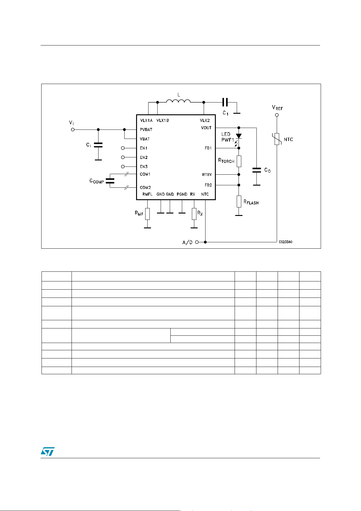
1 Application
Figure 1. Application circuit
Table 1. External components
Symbol Parameter Min. Typ. Max. Unit
R
FLASH
R
TORCH
R
C
C
NTC Negative thermistor - NCP18WF104J03RB - Thick film type 100 kΩ
C
COMP
R
C1 Ceramic Capacitor 47 pF
Sensing flash current resistor - thick film type (0805) 0.27 Ω
Sensing torch current resistor - thick film type (0603) 6.2 Ω
Setting resistor for middle flash mode - thick film type (0402) 8200 Ω
MF
Two Input filtering capacitor TDK C1608X5R0J106MT - Ceramic
I
type (0603) 6.3V
Output capacitance - Ceramic type 0603 6.3V 4.7 µF
O
L TDKVLF5014A-4R7
Compensation capacitor - 0402 100 820 pF
Reference resistor - 0402 15 kΩ
X
INDUCTANCE 4.7 µH
DCR 0.12 Ω
10 2x10 µF
Note: - The external components proposal should be considered as a design reference guide. The
performances mentioned in the electrical characteristics table are not guaranteed for all the
possible electrical parameters of the components included in this list. On the other hand the
operation of STCF02 is not limited with the use of the external components listed above.
- The C
is optional and may be used if the error amplifier bandwidth (which by default is
COMP
set to 2 KHz) has to be decreased because of an unstable driver function. Unstable operation
could be caused by using different values of inductor and output capacitor then recommended.
3/19
Pin connections STCF02
2 Pin connections
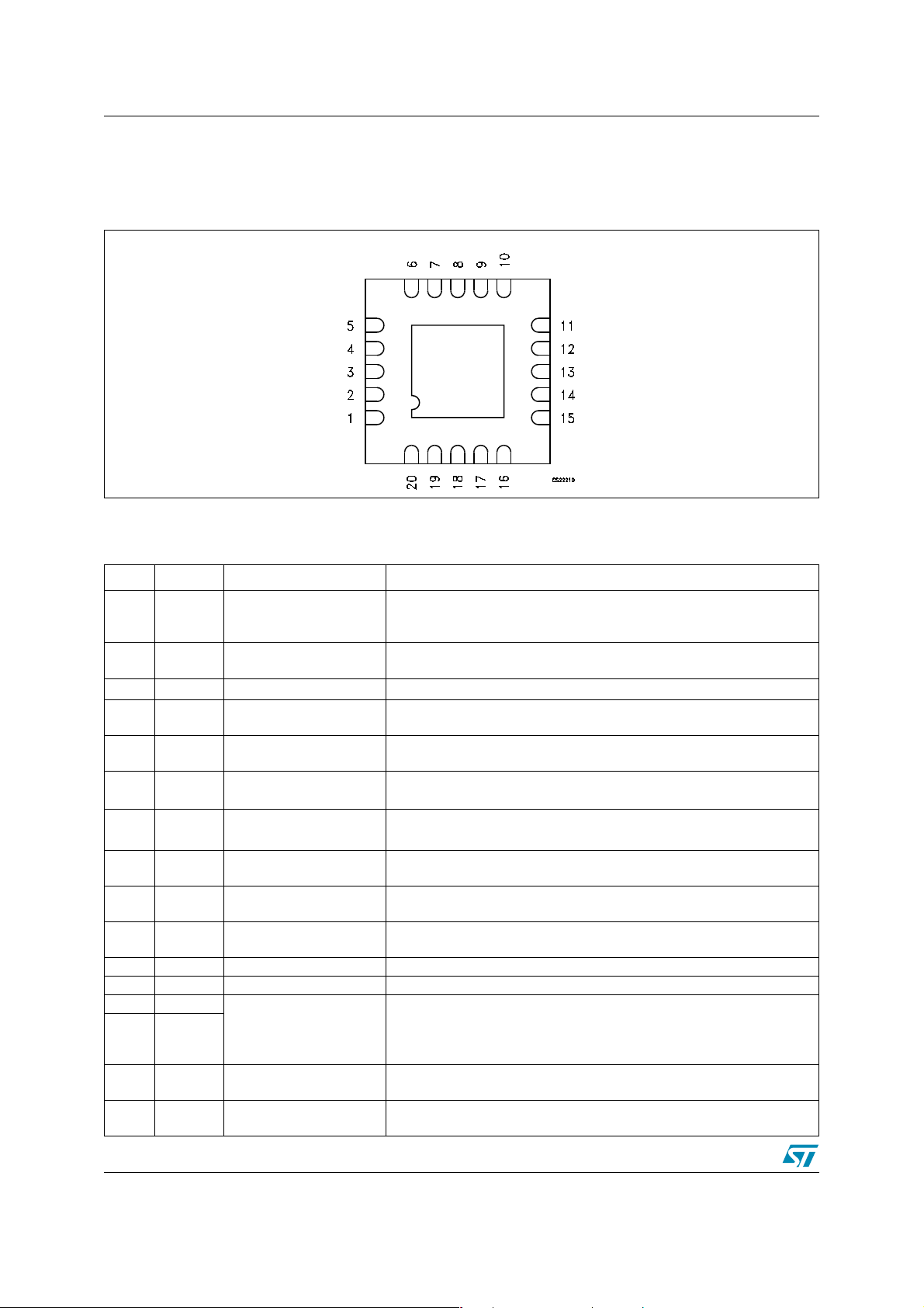
Figure 2. Pin configuration (bottom view)
Table 2. Pin description
Pln N° Symbol Name and function Note
External coil is connected between this pin and VLX1. It should be
1 VLX2 Inductor connection
2 RX Rx Resistor connection
V
3
4 NTC NTC Resistor connection
5FB1
6RTBY
7FB2
8, 10 GND Signal ground
9COM1
11 COM2
12 VBAT Supply voltage Supply pin of the device.
13 PVBAT Power supply voltage Power supply pin of the device.
14 VLX1A
15 VLX1B
16 EN3 Enable Pin 3
17 EN2 Enable Pin 2
Output voltage Anode of the LED is connected to this pin.
O
Feedback pin for torch
mode
TORC H
Bypass
R
Feedback pin for flash
mode
Compensation
connection
Compensation
connection
Inductor connection
placed as close as possible to the device in order to minimize
resistance which cause losses.
Rx resistor is connected between this pin and ground to set LED over
temperature threshold.
This pin is used for the LED temperature sensing using an external
NTC resistor.
This pin is used for current sensing in Torch mode – Cathode of the
Flash LED and RTorch resistor are connected to this pin.
This pin is used to short-circuit the R
MIDDLE FLASH MODE.
This pin is used to sense the voltage across R
directly connected to the non-grounded terminal of R
This is the signal ground pin related to digital and analog signals and
must be connected as close as possible to the sensing resistor.
Optional external compensation should be connected to these pins.
Optional external compensation should be connected to these pins.
External coil is connected between these pins and VLX2. They should
be placed as close as possible to the device in order to minimize
resistance which causes losses. It is mandatory to connect VLX1A
and VLX1B together.
Digital input that allows selection of the operational modes of the
device (refer to truth table).
Digital input that allows selection of the operational modes of the
device (refer to truth table).
during FLASH and
TORCH
FLASH
. It must be
.
FLASH
4/19
STCF02 Pin connections
Pln N° Symbol Name and function Note
18 PGND Power ground
19 RMFL
20 EN1 Enable Pin 1
Exp-
pad
PGND Power ground
Middle flash resistor
connection
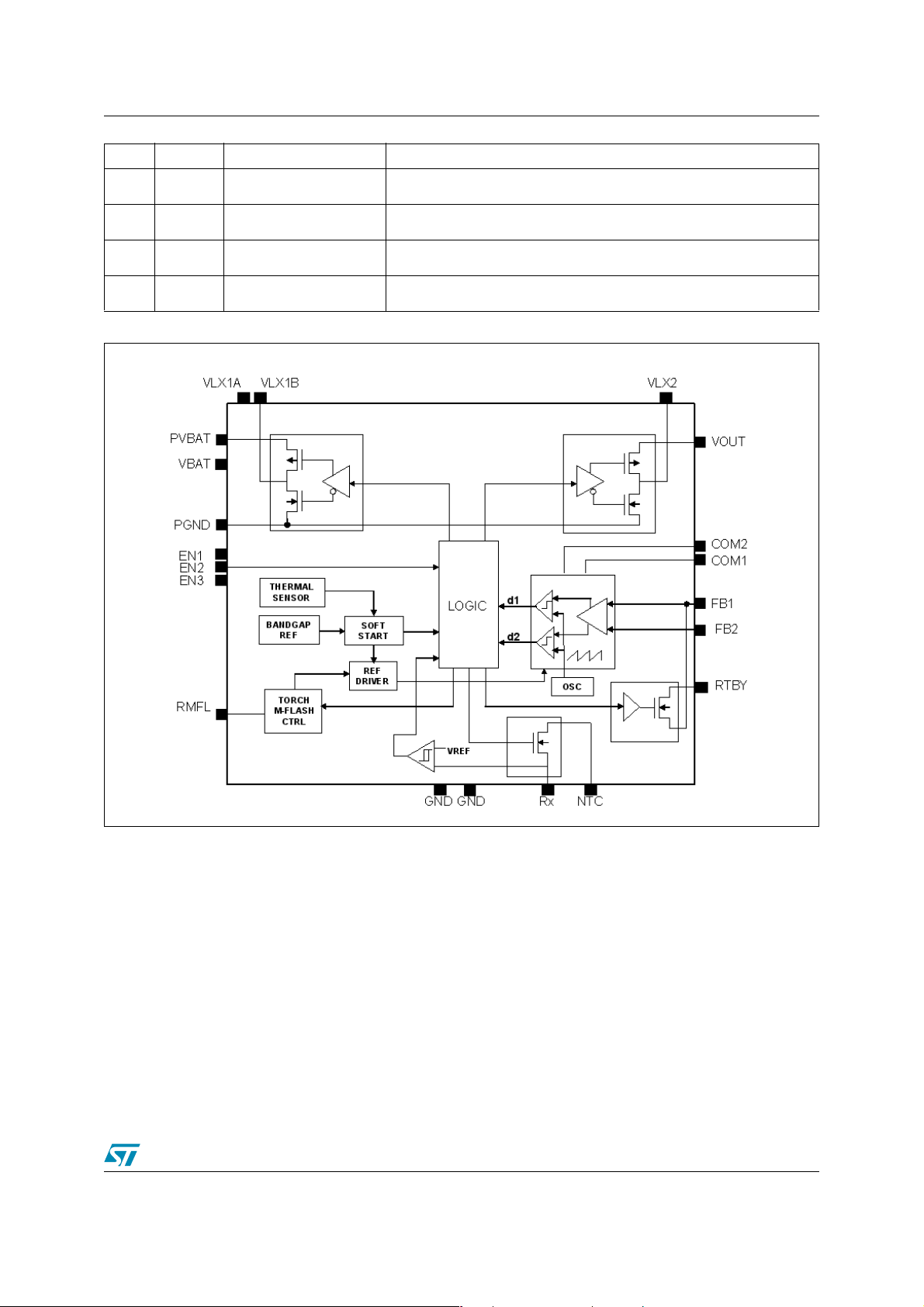
Figure 3. Block diagram
Power ground pin for power analog circuit. To be connected to the
PCB ground plane.
This pin is used for the current setting in Middle Flash Mode – RMF
resistor is connected to this pin.
Digital input that allow selecting the operational modes of the device
(refer to truth table).
To be connected to the PCB Ground Plane for optimal electrical and
thermal performance.
5/19
Maximum ratings STCF02
3 Maximum ratings
Table 3. Absolute maximum ratings
Symbol Parameter Value Unit
VBAT Signal supply voltage -0.3 to 6 V
PVBAT Power supply voltage -0.3 to 6 V
EN1,2,3 Enable input -0.3 to 6 V
V
O
VLX1A-VLX1B Inductor connection 1
VLX2 Inductor connection 2
FB1 Feedback for torch current -0.3 to 3 V
FB2 Feedback for flash current -0.3 to 3 V
RTBY MOS Switch connection -0.3 to 3 V
RX Connection for reference resistor -0.3 to 3 V
RMFL Connection for setting resistor for middle flash -0.3 to 6 V
NTC LED temperature sensing connection -0.3 to 6 V
COM1,COM2 Compensation connection -0.3 to 3 V
T
OP
T
STG
V
ESD
1. STCF02 is guaranteed to meet specification from 0°C to 70°C – specifications over the -40°C to 85°C operating
temperature range are assured by design, characterization and correlation with statistical process control.
Output voltage -0.3 to 6 V
+ 0.3
I
O
+ 0.3
V
V
Ambient operating temperature
(1)
-0.3 to V
-0.3 to V
-40 to + 85 °C
Storage temperature range -65 to + 150 °C
ESD rating 2 KV
Table 4. Thermal data
Symbol Parameter Value Unit
R
thJA
(*) Typical Application on a two layer board.
Thermal resistance junction-ambient (*) 59 °C/W
6/19

STCF02 Characteristics
4 Characteristics
Table 5. Electrical characteristics
(All typical values are referred to T
Symbol Parameter Test Conditions Min. Typ. Max. Unit
V
I
CC
V
UVLO
I
∆I
V
FB1,2 Feedback Voltage Flash Mode 150 160 170 mV
I
e1
e2
I
PK
OVP Over voltage protection
OTP Over temperature protection
OT
HYST
NTC Voltage Reference
NTC
NTC
EN1, EN2,
EN3
I_ENx Enable input current ±1µA
T
FL/TR
T
1. Not include tolerance of sensing resistor
Input Operating Voltage 2.7 5.5 V
I
Under voltage lockout threshold
Output Current Adjustment
Range, I
Output Current Adjustment
O
Range, I
FLASH
MFLASH
Output Current Adjustment
Range, I
Output current variation
O
Regulated voltage range 2.5 5.1 V
O
Quiescent Current in Stand By
Q
f
Frequency
TORCH
Efficiency
Inductor peak current
Overtemperature hysteresis
Hysteresis 0.3 V
HYST
Voltage Reference leakage EN1=EN2=0, EN3=X ±1µA
LEAK
Logic signals level
Transition time from PIN (Flash)
to PIN (Torch) (see
Led current rise time I
ON
I
= max (see
LED
Figure 11
Figure 13
LED
)
= 0 to
)
= 25°C, VI = 3.6V)
A
Torch mode 616 686 757
µAMedium flash mode 590 688 733
Flash mode 555 660 728
rising
V
I
VI falling
5.1 5.3
5.1 5.3
V
Flash mode for VI = 2.7V to 4.5V
R
FLASH_MIN
R
FLASH_MAX
Medium flash mode for VI = 2.7V to
4.5V RM
RM
FLASH_MAX
=1.6Ω to
=0.27Ω
FLASH_MIN
=500kΩ
=1.1kΩ to
100 600
25%
I
FLASH
I
FLASH
mA
Torch mode VI = 2.7V to 4.5V
R
TORCH+RFLASH
R
TORCH+RFLASH
Flash and medium flash mode
=6.4Ω to
=0.64Ω
(1)
25 250
±10 %
Torch mode ±5%
EN1=EN2=EN3=0 1
EN1=EN2=0 EN3=X (NTC ON) 3
VI = 2.7V
Application Circuit
Figure 2
VI = 3.2 V to 4.2V, IO=600mA
Application Circuit
Figure 2
VI = 3.2 V to 4.2V, IO=25mA
= 2.7V, IO=600mA
V
I
V
= 4.2V No load
I
= 2.7V to 4.5V (
V
I
= 2.7V to 4.5V (
V
I
VI = 4V, I
NTC
Disable Low V
Enable High V
Note: 1
Note: 1
= 2mA max
IL
IH
)
)
78 85 %
72 75 %
5.2 V
1.4
1.8 MHz
1.23 A
140 °C
1.192 V
PIN (IO=600mA) to PIN
(IO=100mA) (
Note: 1
)
EN1=EN2=0 to EN1=0 & EN2=1
or EN1=EN2=1 (Note 1)
20 °C
0.4
µA
V
30 µs
2ms
Note: 1 Guaranteed by design
7/19

Characteristics STCF02
Table 6. Truth table selection mode
EN1 EN2 EN3
I
LED
I
LED_MAX
(mA)
Mode NTC
0 0 X 0 0 Shutdown OFF
1 0 1 0 0 Shutdown ON
01X I
I
MFLASH
I
FLASH
(R
111
100
110
=160mV/
TORCH
TORCH+RFLASH
= f (I
FLASH,RMFLASH
= 160mV/R
)
FLASH
250 Torch ON
)
500 Medium Flash ON
600 Flash ON
8/19

STCF02 Typical characteristics
5 Typical characteristics
Figure 4. IIN vs VIN in torch mode Figure 5. IO vs VIN in torch mode 25 mA
Figure 6. IO vs VIN in flash mode 600 mA Figure 7. VFB1 vs temp in torch mode
Figure 8. Efficiency vs IO in torch mode Figure 9. Start-up to torch mode 25 mA at
V
= 3.6V
BATT
9/19

Typical characteristics STCF02
Figure 10. Start-up to flash mode 600 mA at
V
= 3.6V
BATT
10/19

STCF02 Detailed operating description
6 Detailed operating description
6.1 Introduction
The STCF02 is a buck-boost converter, dedicated to power and control the current of a Power White Led
in a camera cell Phone. The device operates at a constant switching frequency of 1.8MHz typ. It provides
an output voltage down to 2.5V and up to 5.1 V, from a single cell 2.7 V to 5.5 V lithium-ion battery. The
flash current is adjustable from 100mA to 600mA for the input voltage range from 2.7V to 4.5V. Torch
current is adjustable from 25mA to 250mA. The device also includes a medium flash mode with the
current set between the 25% of flash current and flash current. The device contains a pin for connection
of NTC which senses the temperature of the LED.
6.2 Buck-Boost converter
Regulation of the PWM controller is made by sensing the current of the led through the R
(see
Figure 2
). Depending on the forward voltage of the Flash LED, the device can automatically change
FLASH
resistor
the operation mode between buck (step down) and boost (step up) mode. Three case can occur:
Boost region (V
I
x R
LED
FLASH
> VBAT): this configuration is used in most cases, as the output voltage (VO = V
O
) is higher than VBAT; Buck region (VO < V
); Buck / Boost region (VO ~ VI).
BAT
fLED
6.3 Flash mode
To select Flash mode the Enable pins have to be connected as follows: EN1=1, EN2=1, EN3=0.
The STCF02 operates continuously to supply maximum current to the flash LED (up to 600 mA).
The flash current can be adjusted by the R
voltage across R
I
= 160mV / R
FLASH
. The flash current is then programmed at:
FLASH
FLASH.
For a flash current programmed at 600mA, the sensing resistor is equal to 0.27Ω.
During this operation mode the MOS Switch between FB1 and RTBY pins is closed.
If the EN3 is forced to High during Flash mode operation, the current is reduced to that of Torch mode.
Such reduction of input power during transition from Flash to Torch mode is achieved within less than
30µs. The NTC divider for measuring LED temperature is active.
resistor. The control loop uses the FB2 pin to sense the
FLASH
+
11/19

Detailed operating description STCF02
Figure 11. Reducing power during the EN3
6.4 Medium flash mode
To select this operating mode the Enable pins have to be connected as follows:
EN1=1, EN2=0, EN3=0
In medium flash mode the current is set between the Torch and the flash mode levels and can be adjusted
by connecting a resistor between the RMFL pin and the ground:
The medium flash current is then programmed using the following equation:
I
=10-5/RFL • [3000+(13000• RMF/13000+RMF)]. (See
MF
Figure 12
).
12/19

STCF02 Detailed operating description
Figure 12. Middle Flash Current (as a percentage of flash current) vs RMF
6.5 Torch mode
To select this operating mode the Enable pins have to be connected to any one of the follow states:
EN1 = 0, EN2 = 1, EN3 = x
EN1 = 1, EN2 = 1, EN3 = 1.
The STCF02 can continuously provide a torch current adjustable between 25mA and 250mA. The torch
current adjustment is made by resistor R
voltage across R
I
TORCH
=160mV/(R
FLASH+RTORCH
FLASH+RTORCH
. The torch current is then programmed using the following equation:
).
If the programmed Flash current is 600mA (R
R
resistance is equal to 0.37Ω.
TORCH
TORCH
(
Figure 2
FLASH
). The control loop uses the FB1 pin to sense the
= 0.27Ω) and a 250mA Torch current is needed, the
During Torch operation mode the MOS Switch between FB1 and RTBY pins is opened.
The NTC divider for measuring LED temperature is active.
6.6 Shutdown mode
When the device is not used, two shutdown modes are available. They can be selected by the enable
pins:
EN1=0, EN2=0, EN3=X
With this combination the NTC divider for measuring of LED temperature is not active. The quiescent
current is less than 1µA.
EN=1, EN2=0, EN3=1
This combination of enable pins provides shutdown modes with an active NTC divider for sensing LED
temperature. This Mode is useful for measuring the temperature before starting both TORCH and FLASH
MODE operations.
13/19

Detailed operating description STCF02
6.7 Soft start
To avoid spikes the battery during start-up sequence, a soft start function has been implemented. This
soft start is achieved by progressively increasing the feedback voltage reference. In the worst case
scenario the start up time as defined below (I
Figure 13. Start up - LED current rise time
O
= I
) will not exceed 6ms.
MAX
6.8 LED Failure Protection
The device is self protected when the LED fails as a result of a short or open circuit. Such performances
are tested using a standard mobile phone Lithium battery with internal resistance 170mΩ typ.
6.9 Overvoltage protection
The device includes a power switch protection that stops the operation of the PWM controller when the
voltage at the pin V
exceeds the OVP threshold.
O
6.10 Thermal shutdown protection
Internal thermal shutdown protection will switch off the device when the junction temperature exceeds
140°C typical. The hysteresis comparator allows for the automatic restart of the PWM controller, when the
temperature is reduced by 20°C.
6.11 Sensing of LED temperature by NTC resistor
The device is able to switch off the power circuit, if high temperature on the LED is detected (see
Figure 14
).
14/19

STCF02 Detailed operating description
6.12 Safety shutdown in flash mode
To avoid LED burning during flash mode, which could be brought on by a micro-controller fault, a simple
programmable R
Figure 15
).
Figure 14. Typical application of LED temperature sensing by NTC resistor
circuit is possible to shutdown the device after a selected time through the RX Pin (see
C
Figure 15. Typical Application of Safety Shutdown
EN1 EN2 Mode
0 0 All OFF N/A
01 Torch NO
1 0 Mid-Flash YES
1 1 Full-Flash YES
Time-
Out
15/19

Package mechanical data STCF02
7 Package mechanical data
In order to meet environmental requirements, ST offers these devices in ECOPACK® packages.
These packages have a Lead-free second level interconnect. The category of second level
interconnect is marked on the package and on the inner box label, in compliance with JEDEC
Standard JESD97. The maximum ratings related to soldering conditions are also marked on
the inner box label. ECOPACK is an ST trademark. ECOPACK specifications are available at:
www.st.com.
16/19

STCF02 Package mechanical data
QFN20 (4x4) MECHANICAL DATA
mm. mils
DIM.
MIN. TYP MAX. MIN. TYP. MAX.
A 0.8 0.9 1.0031.535.439.4
A1 0.02 0.05 0.8 2.0
A2 0.65 1.00 25.6 39.4
A3 0.25 9.8
b 0.18 0.23 0.30 7.1 9.1 11.8
D 3.875 4.00 4.125 152.6 157.5 162.4
D2 0.75 1.7 2.25 29.5 66.9 88.6
E 3.875 4.00 4.125 152.6 157.5 162.4
E2 0.75 1.7 2.25 29.5 66.9 88.6
e 0.450.500.5517.719.721.7
L 0.350.550.7513.821.725.9
ddd 0.08 3.1
7169619-D
17/19

Revision history STCF02
8 Revision history
Table 7. Revision history
Date Revision Changes
10-Nov-2005 1 First release.
19-Dec-2005 2 Document updating.
29-Jun-2006 3 The table 5 has been updated and add typical characteristics.
27-Jul-2006 4
18-Oct-2006 5 Text updates.
Mistake on table 5 figure reference T
FL/TR
parameter.
09-Feb-2007 6
Mistake value of IO test condition RM
FLASH_MAX
= 500Ω ==> 500kΩ on
Ta b l e 5 .
18/19

STCF02
Please Read Carefully:
Information in this document is provided solely in connection with ST products. STMicroelectronics NV and its subsidiaries (“ST”) reserve the
right to make changes, corrections, modifications or improvements, to this document, and the products and services described herein at any
time, without notice.
All ST products are sold pursuant to ST’s terms and conditions of sale.
Purchasers are solely responsible for the choice, selection and use of the ST products and services described herein, and ST assumes no
liability whatsoever relating to the choice, selection or use of the ST products and services described herein.
No license, express or implied, by estoppel or otherwise, to any intellectual property rights is granted under this document. If any part of this
document refers to any third party products or services it shall not be deemed a license grant by ST for the use of such third party products
or services, or any intellectual property contained therein or considered as a warranty covering the use in any manner whatsoever of such
third party products or services or any intellectual property contained therein.
UNLESS OTHERWISE SET FORTH IN ST’S TERMS AND CONDITIONS OF SALE ST DISCLAIMS ANY EXPRESS OR IMPLIED
WARRANTY WITH RESPECT TO THE USE AND/OR SALE OF ST PRODUCTS INCLUDING WITHOUT LIMITATION IMPLIED
WARRANTIES OF MERCHANTABILITY, FITNESS FOR A PARTICULAR PURPOSE (AND THEIR EQUIVALENTS UNDER THE LAWS
OF ANY JURISDICTION), OR INFRINGEMENT OF ANY PATENT, COPYRIGHT OR OTHER INTELLECTUAL PROPERTY RIGHT.
UNLESS EXPRESSLY APPROVED IN WRITING BY AN AUTHORIZED ST REPRESENTATIVE, ST PRODUCTS ARE NOT
RECOMMENDED, AUTHORIZED OR WARRANTED FOR USE IN MILITARY, AIR CRAFT, SPACE, LIFE SAVING, OR LIFE SUSTAINING
APPLICATIONS, NOR IN PRODUCTS OR SYSTEMS WHERE FAILURE OR MALFUNCTION MAY RESULT IN PERSONAL INJURY,
DEATH, OR SEVERE PROPERTY OR ENVIRONMENTAL DAMAGE. ST PRODUCTS WHICH ARE NOT SPECIFIED AS "AUTOMOTIVE
GRADE" MAY ONLY BE USED IN AUTOMOTIVE APPLICATIONS AT USER’S OWN RISK.
Resale of ST products with provisions different from the statements and/or technical features set forth in this document shall immediately void
any warranty granted by ST for the ST product or service described herein and shall not create or extend in any manner whatsoever, any
liability of ST.
ST and the ST logo are trademarks or registered trademarks of ST in various countries.
Information in this document supersedes and replaces all information previously supplied.
The ST logo is a registered trademark of STMicroelectronics. All other names are the property of their respective owners.
© 2007 STMicroelectronics - All rights reserved
STMicroelectronics group of companies
Australia - Belgium - Brazil - Canada - China - Czech Republic - Finland - France - Germany - Hong Kong - India - Israel - Italy - Japan -
Malaysia - Malta - Morocco - Singapore - Spain - Sweden - Switzerland - United Kingdom - United States of America
www.st.com
19/19
 Loading...