

Page 1
M41T82
M41T83
Serial I2C bus real-time clock (RTC) with battery switchover
Datasheet − production data
Features
■ Ultra-low battery supply current of 365 nA
■ Factory calibrated accuracy ±5 ppm
guaranteed after 2 reflows (SOX18)
– Much better accuracies achievable using
built-in programmable analog and digital
calibration circuits
■ 2.0 V to 5.5 V clock operating voltage
■ Counters for tenths/hundredths of seconds,
seconds, minutes, hours, day, date, month,
year, and century
■ Automatic switchover and reset output circuitry
(fixed reference)
–M41T83S
V
= 3.00 V to 5.50 V
CC
(2.85 V ≤ V
–M41T83R
V
= 2.70 V to 5.50 V
CC
(2.55 V ≤ V
–M41T83Z
V
= 2.38 V to 5.50 V
CC
(2.25 V ≤ V
■ Serial interface supports I
protocol)
■ Programmable alarm with interrupt function
(valid even during battery backup mode)
■ Optional 2
■ Square wave output defaults to 32 KHz on
nd
power-up (M41T83 only)
■ RESET (RST) output
■ Watchdog timer
■ Programmable 8-bit counter/timer
■ 7 bytes of battery-backed user SRAM
■ Battery low flag
■ Low operating current of 80 µA
≤ 3.00 V)
RST
≤ 2.70 V)
RST
≤ 2.38 V)
RST
2
C bus (400 kHz
programmable alarm available
QFN16, 4 mm x 4 mm
(VFQFPN16)
18
1
SOX18 (18-pin, 300 mil SOIC
with embedded crystal)
SO8
■ Oscillator stop detection
■ Battery or SuperCap™ backup
■ Operating temperature of –40 °C to 85 °C
■ Package options
– a 16-lead QFN (M41T83),
– an 18-lead embedded crystal SOIC
(M41T83), or
– an 8-lead SOIC (M41T82)
■ RoHS compliance: lead-free components are
compliant with the RoHS directive
May 2012 Doc ID 12578 Rev 14 1/63
This is information on a product in full production.
www.st.com
1
Page 2

Contents M41T82-M41T83
Contents
1 Description . . . . . . . . . . . . . . . . . . . . . . . . . . . . . . . . . . . . . . . . . . . . . . . . . 6
2 Operation . . . . . . . . . . . . . . . . . . . . . . . . . . . . . . . . . . . . . . . . . . . . . . . . . 12
2.1 2-wire bus characteristics . . . . . . . . . . . . . . . . . . . . . . . . . . . . . . . . . . . . . 13
2.1.1 Bus not busy . . . . . . . . . . . . . . . . . . . . . . . . . . . . . . . . . . . . . . . . . . . . . 13
2.1.2 Start data transfer . . . . . . . . . . . . . . . . . . . . . . . . . . . . . . . . . . . . . . . . . 13
2.1.3 Stop data transfer . . . . . . . . . . . . . . . . . . . . . . . . . . . . . . . . . . . . . . . . . 13
2.1.4 Data valid . . . . . . . . . . . . . . . . . . . . . . . . . . . . . . . . . . . . . . . . . . . . . . . . 13
2.1.5 Acknowledge . . . . . . . . . . . . . . . . . . . . . . . . . . . . . . . . . . . . . . . . . . . . . 14
2.2 Read mode . . . . . . . . . . . . . . . . . . . . . . . . . . . . . . . . . . . . . . . . . . . . . . . . 15
2.3 Write mode . . . . . . . . . . . . . . . . . . . . . . . . . . . . . . . . . . . . . . . . . . . . . . . . 17
2.4 Data retention and battery switchover (V
2.5 Power-on reset (t
) . . . . . . . . . . . . . . . . . . . . . . . . . . . . . . . . . . . . . . . . . 18
rec
SO
= V
) . . . . . . . . . . . . . . . . 18
RST
3 Clock operation . . . . . . . . . . . . . . . . . . . . . . . . . . . . . . . . . . . . . . . . . . . . 19
3.1 Clock data coherency . . . . . . . . . . . . . . . . . . . . . . . . . . . . . . . . . . . . . . . . 20
3.1.1 Example of incoherency . . . . . . . . . . . . . . . . . . . . . . . . . . . . . . . . . . . . 20
3.1.2 Accessing the device . . . . . . . . . . . . . . . . . . . . . . . . . . . . . . . . . . . . . . . 21
3.2 Halt bit (HT) operation . . . . . . . . . . . . . . . . . . . . . . . . . . . . . . . . . . . . . . . 21
3.2.1 Power-down time-stamp . . . . . . . . . . . . . . . . . . . . . . . . . . . . . . . . . . . . 22
3.3 Real-time clock accuracy . . . . . . . . . . . . . . . . . . . . . . . . . . . . . . . . . . . . . 27
3.4 Clock calibration . . . . . . . . . . . . . . . . . . . . . . . . . . . . . . . . . . . . . . . . . . . . 28
3.4.1 Digital calibration (periodic counter correction) . . . . . . . . . . . . . . . . . . . 28
3.4.2 Analog calibration (programmable load capacitance) . . . . . . . . . . . . . . 31
3.5 Setting the alarm clock registers . . . . . . . . . . . . . . . . . . . . . . . . . . . . . . . 35
3.6 Optional second programmable alarm and user SRAM . . . . . . . . . . . . . . 36
3.7 Watchdog timer . . . . . . . . . . . . . . . . . . . . . . . . . . . . . . . . . . . . . . . . . . . . 36
3.8 8-bit (countdown) timer . . . . . . . . . . . . . . . . . . . . . . . . . . . . . . . . . . . . . . . 37
3.8.1 M41T83 timer interrupt/output . . . . . . . . . . . . . . . . . . . . . . . . . . . . . . . . 37
3.8.2 Timer flag (TF) . . . . . . . . . . . . . . . . . . . . . . . . . . . . . . . . . . . . . . . . . . . . 39
3.8.3 Timer interrupt enable (TIE, M41T83 only) . . . . . . . . . . . . . . . . . . . . . . 39
3.8.4 Timer enable (TE) . . . . . . . . . . . . . . . . . . . . . . . . . . . . . . . . . . . . . . . . . 39
3.8.5 TD1/0 . . . . . . . . . . . . . . . . . . . . . . . . . . . . . . . . . . . . . . . . . . . . . . . . . . . 39
2/63 Doc ID 12578 Rev 14
Page 3

M41T82-M41T83 Contents
3.9 Square wave output (M41T83 only) . . . . . . . . . . . . . . . . . . . . . . . . . . . . . 39
3.10 Battery low warning . . . . . . . . . . . . . . . . . . . . . . . . . . . . . . . . . . . . . . . . . 41
3.11 Century bits . . . . . . . . . . . . . . . . . . . . . . . . . . . . . . . . . . . . . . . . . . . . . . . 42
3.12 Oscillator fail detection . . . . . . . . . . . . . . . . . . . . . . . . . . . . . . . . . . . . . . . 42
3.13 Oscillator fail interrupt enable (M41T83 only) . . . . . . . . . . . . . . . . . . . . . . 43
3.14 IRQ1
/FT/OUT pin, frequency test, interrupts and the OUT bit
(M41T83 only) . . . . . . . . . . . . . . . . . . . . . . . . . . . . . . . . . . . . . . . . . . . . . 43
3.14.1 Active mode operation on V
3.14.2 Backup mode . . . . . . . . . . . . . . . . . . . . . . . . . . . . . . . . . . . . . . . . . . . . . 45
CC . . . . . . . . . . . . . . . . . . . . . . . . . . . . . . . . . . . . . . . . 44
3.15 FT/RST pin, frequency test and reset output pin (M41T82 only) . . . . . . . 46
3.16 Initial power-on defaults . . . . . . . . . . . . . . . . . . . . . . . . . . . . . . . . . . . . . . 46
3.17 OTP bit operation (M41T83 in SOX18 package only) . . . . . . . . . . . . . . . 47
4 Maximum ratings . . . . . . . . . . . . . . . . . . . . . . . . . . . . . . . . . . . . . . . . . . . 48
5 DC and AC parameters . . . . . . . . . . . . . . . . . . . . . . . . . . . . . . . . . . . . . . 49
6 Package mechanical data . . . . . . . . . . . . . . . . . . . . . . . . . . . . . . . . . . . . 54
7 Part numbering . . . . . . . . . . . . . . . . . . . . . . . . . . . . . . . . . . . . . . . . . . . . 60
8 References . . . . . . . . . . . . . . . . . . . . . . . . . . . . . . . . . . . . . . . . . . . . . . . . 61
9 Revision history . . . . . . . . . . . . . . . . . . . . . . . . . . . . . . . . . . . . . . . . . . . 62
Doc ID 12578 Rev 14 3/63
Page 4

List of tables M41T82-M41T83
List of tables
Table 1. Signal names . . . . . . . . . . . . . . . . . . . . . . . . . . . . . . . . . . . . . . . . . . . . . . . . . . . . . . . . . . . . 8
Table 2. M41T82 clock/control register map (32 bytes) . . . . . . . . . . . . . . . . . . . . . . . . . . . . . . . . . . 23
Table 3. Key to Table 2: M41T82 clock/control register map (32 bytes). . . . . . . . . . . . . . . . . . . . . . 24
Table 4. M41T83 clock/control register map (32 bytes) . . . . . . . . . . . . . . . . . . . . . . . . . . . . . . . . . . 25
Table 5. Key to Table 4: M41T83 clock/control register map (32 bytes). . . . . . . . . . . . . . . . . . . . . . 26
Table 6. Digital calibration values . . . . . . . . . . . . . . . . . . . . . . . . . . . . . . . . . . . . . . . . . . . . . . . . . . . 30
Table 7. Analog calibration values . . . . . . . . . . . . . . . . . . . . . . . . . . . . . . . . . . . . . . . . . . . . . . . . . . 32
Table 8. Alarm repeat modes . . . . . . . . . . . . . . . . . . . . . . . . . . . . . . . . . . . . . . . . . . . . . . . . . . . . . . 36
Table 9. Watchdog register. . . . . . . . . . . . . . . . . . . . . . . . . . . . . . . . . . . . . . . . . . . . . . . . . . . . . . . . 37
Table 10. Timer control register map . . . . . . . . . . . . . . . . . . . . . . . . . . . . . . . . . . . . . . . . . . . . . . . . . 38
Table 11. Timer interrupt operation in free-running mode (with TI
Table 12. Timer source clock frequency selection (244.1 µs to 4.25 hrs). . . . . . . . . . . . . . . . . . . . . . 39
Table 13. Square wave output frequency . . . . . . . . . . . . . . . . . . . . . . . . . . . . . . . . . . . . . . . . . . . . . . 40
Table 14. Century bits examples . . . . . . . . . . . . . . . . . . . . . . . . . . . . . . . . . . . . . . . . . . . . . . . . . . . . 42
Table 15. Priority for IRQ1
Table 16. Priority for IRQ1/FT/OUT pin when operating in backup mode . . . . . . . . . . . . . . . . . . . . . 45
Table 17. Initial power-on default values (part 1) . . . . . . . . . . . . . . . . . . . . . . . . . . . . . . . . . . . . . . . . 46
Table 18. Initial power-up default values (part 2) . . . . . . . . . . . . . . . . . . . . . . . . . . . . . . . . . . . . . . . . 46
Table 19. Absolute maximum ratings . . . . . . . . . . . . . . . . . . . . . . . . . . . . . . . . . . . . . . . . . . . . . . . . . 48
Table 20. Operating and AC measurement conditions . . . . . . . . . . . . . . . . . . . . . . . . . . . . . . . . . . . . 49
Table 21. Capacitance . . . . . . . . . . . . . . . . . . . . . . . . . . . . . . . . . . . . . . . . . . . . . . . . . . . . . . . . . . . . 49
Table 22. DC characteristics. . . . . . . . . . . . . . . . . . . . . . . . . . . . . . . . . . . . . . . . . . . . . . . . . . . . . . . . 50
Table 23. Crystal electrical characteristics . . . . . . . . . . . . . . . . . . . . . . . . . . . . . . . . . . . . . . . . . . . . . 51
Table 24. Oscillator characteristics . . . . . . . . . . . . . . . . . . . . . . . . . . . . . . . . . . . . . . . . . . . . . . . . . . . 51
Table 25. Power down/up trip points DC characteristics . . . . . . . . . . . . . . . . . . . . . . . . . . . . . . . . . . 52
Table 26. AC characteristics. . . . . . . . . . . . . . . . . . . . . . . . . . . . . . . . . . . . . . . . . . . . . . . . . . . . . . . . 53
Table 27. QFN16 – 16-lead, quad, flat package, no lead, 4 x 4 mm pack. mech. data . . . . . . . . . . . 55
Table 28. SOX18 – 18-lead plastic small outline, 300 mils, embedded crystal, package mech. data 57
Table 29. SO8 – 8-lead plastic small outline (150 mils body width), package mech. data . . . . . . . . . 58
Table 30. Carrier tape dimensions for QFN16, SOX18, and SO8 packages . . . . . . . . . . . . . . . . . . . 59
Table 31. Ordering information . . . . . . . . . . . . . . . . . . . . . . . . . . . . . . . . . . . . . . . . . . . . . . . . . . . . . . 60
Table 32. Document revision history . . . . . . . . . . . . . . . . . . . . . . . . . . . . . . . . . . . . . . . . . . . . . . . . . 62
/FT/OUT pin when operating on V
/TP = 1). . . . . . . . . . . . . . . . . . . . . 38
CC . . . . . . . . . . . . . . . . . . . . . . . . . . . . . . . . . . . . 44
4/63 Doc ID 12578 Rev 14
Page 5

M41T82-M41T83 List of figures
List of figures
Figure 1. M41T82 logic diagram . . . . . . . . . . . . . . . . . . . . . . . . . . . . . . . . . . . . . . . . . . . . . . . . . . . . . 7
Figure 2. M41T83 logic diagram . . . . . . . . . . . . . . . . . . . . . . . . . . . . . . . . . . . . . . . . . . . . . . . . . . . . . 7
Figure 3. SO8 (M) connections (M41T82) . . . . . . . . . . . . . . . . . . . . . . . . . . . . . . . . . . . . . . . . . . . . . . 9
Figure 4. QFN16 (QA) connections (M41T83). . . . . . . . . . . . . . . . . . . . . . . . . . . . . . . . . . . . . . . . . . . 9
Figure 5. SOX18 (MY) connections (M41T83). . . . . . . . . . . . . . . . . . . . . . . . . . . . . . . . . . . . . . . . . . . 9
Figure 6. M41T82 block diagram . . . . . . . . . . . . . . . . . . . . . . . . . . . . . . . . . . . . . . . . . . . . . . . . . . . . 10
Figure 7. M41T82 hardware hookup . . . . . . . . . . . . . . . . . . . . . . . . . . . . . . . . . . . . . . . . . . . . . . . . . 10
Figure 8. M41T83 block diagram . . . . . . . . . . . . . . . . . . . . . . . . . . . . . . . . . . . . . . . . . . . . . . . . . . . . 11
Figure 9. M41T83 hardware hookup . . . . . . . . . . . . . . . . . . . . . . . . . . . . . . . . . . . . . . . . . . . . . . . . . 11
Figure 10. Serial bus data transfer sequence . . . . . . . . . . . . . . . . . . . . . . . . . . . . . . . . . . . . . . . . . . . 14
Figure 11. Acknowledgement sequence . . . . . . . . . . . . . . . . . . . . . . . . . . . . . . . . . . . . . . . . . . . . . . . 14
Figure 12. Slave address location . . . . . . . . . . . . . . . . . . . . . . . . . . . . . . . . . . . . . . . . . . . . . . . . . . . . 15
Figure 13. Read mode sequence. . . . . . . . . . . . . . . . . . . . . . . . . . . . . . . . . . . . . . . . . . . . . . . . . . . . . 16
Figure 14. Alternative read mode sequence . . . . . . . . . . . . . . . . . . . . . . . . . . . . . . . . . . . . . . . . . . . . 16
Figure 15. Write mode sequence . . . . . . . . . . . . . . . . . . . . . . . . . . . . . . . . . . . . . . . . . . . . . . . . . . . . . 17
Figure 16. Clock data coherency . . . . . . . . . . . . . . . . . . . . . . . . . . . . . . . . . . . . . . . . . . . . . . . . . . . . . 20
Figure 17. Internal load capacitance adjustment . . . . . . . . . . . . . . . . . . . . . . . . . . . . . . . . . . . . . . . . . 27
Figure 18. Crystal accuracy across temperature . . . . . . . . . . . . . . . . . . . . . . . . . . . . . . . . . . . . . . . . . 32
Figure 19. Clock accuracy vs. on-chip load capacitance . . . . . . . . . . . . . . . . . . . . . . . . . . . . . . . . . . . 33
Figure 20. Clock divider chain and calibration circuits . . . . . . . . . . . . . . . . . . . . . . . . . . . . . . . . . . . . . 34
Figure 21. Crystal isolation example . . . . . . . . . . . . . . . . . . . . . . . . . . . . . . . . . . . . . . . . . . . . . . . . . . 35
Figure 22. Timer output waveform in free-running mode (with TI
Figure 23. Battery check . . . . . . . . . . . . . . . . . . . . . . . . . . . . . . . . . . . . . . . . . . . . . . . . . . . . . . . . . . . 41
Figure 24. IRQ1
Figure 25. Measurement AC I/O waveform . . . . . . . . . . . . . . . . . . . . . . . . . . . . . . . . . . . . . . . . . . . . . 49
Figure 26. I
Figure 27. Power down/up mode AC waveforms. . . . . . . . . . . . . . . . . . . . . . . . . . . . . . . . . . . . . . . . . 52
Figure 28. Bus timing requirement sequence . . . . . . . . . . . . . . . . . . . . . . . . . . . . . . . . . . . . . . . . . . . 53
Figure 29. QFN16 – 16-lead, quad, flat package, no lead, 4 x 4 mm body size outline . . . . . . . . . . . 55
Figure 30. QFN16 – 16-lead, quad, flat package, no lead, 4 x 4 mm, recommended footprint . . . . . . 56
Figure 31. 32 KHz crystal + QFN16 vs. VSOJ20 mechanical data . . . . . . . . . . . . . . . . . . . . . . . . . . . 56
Figure 32. SOX18 – 18-lead plastic small outline, 300 mils, embedded crystal, outline . . . . . . . . . . . 57
Figure 33. SO8 – 8-lead plastic small package outline . . . . . . . . . . . . . . . . . . . . . . . . . . . . . . . . . . . . 58
Figure 34. Carrier tape for QFN16, SOX18, and SO8 packages . . . . . . . . . . . . . . . . . . . . . . . . . . . . . 59
/FT/OUT output pin circuit . . . . . . . . . . . . . . . . . . . . . . . . . . . . . . . . . . . . . . . . . . . . . 43
vs. temperature . . . . . . . . . . . . . . . . . . . . . . . . . . . . . . . . . . . . . . . . . . . . . . . . . . . . . . 51
CC2
/TP = 1) . . . . . . . . . . . . . . . . . . . . . . 38
Doc ID 12578 Rev 14 5/63
Page 6

Description M41T82-M41T83
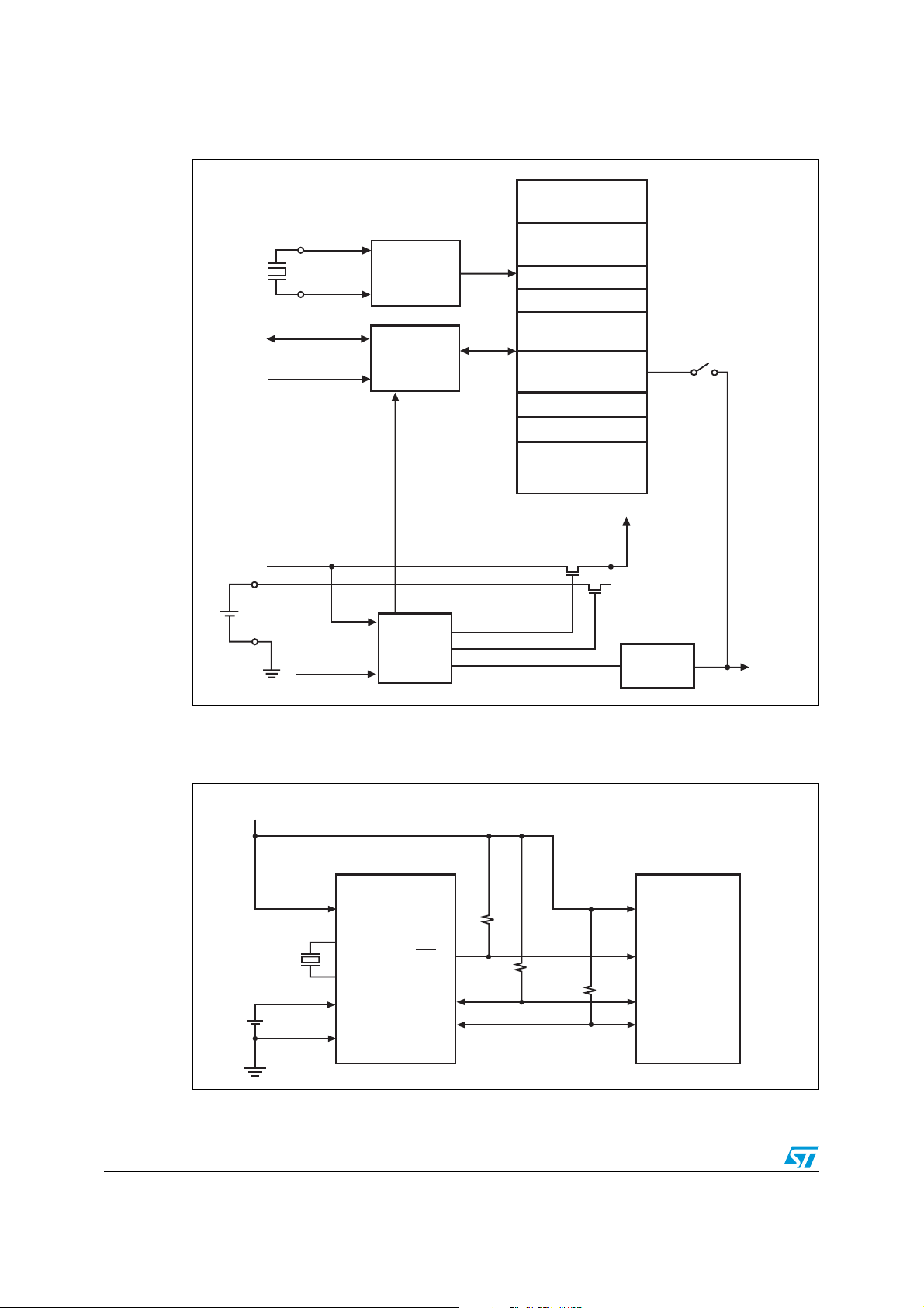
1 Description
The M41T8x are low-power serial I2C real-time clocks (RTCs) with a built-in 32.768 kHz
oscillator (external crystal-controlled for the QFN16 and SO8 packages, embedded crystal
for the SOX18 package). Eight bytes of the register map (see Table 2 on page 23) are used
for the clock/calendar function and are configured in binary-coded decimal (BCD) format. An
additional 17 bytes of the register map provide status/control of the two alarms, watchdog,
8-bit counter, and square wave functions. An additional seven bytes are made available as
user SRAM.
Addresses and data are transferred serially via a two-line, bidirectional I
built-in address register is incremented automatically after each WRITE or READ data byte.
The M41T8x has a built-in power sense circuit which detects power failures and
automatically switches to the battery supply when a power failure occurs. The energy
needed to sustain the clock operations can be supplied by a small lithium button battery
when a power failure occurs.
Functions available to the user include a non-volatile, time-of-day clock/calendar, two alarm
interrupts, watchdog timer, programmable 8-bit counter, and square wave outputs. The eight
clock address locations contain the century, year, month, date, day, hour, minute, second,
and tenths/hundredths of a second in 24-hour BCD format. Corrections for 28, 29 (leap
year), 30, and 31 day months are made automatically. The M41T83 is supplied in either a
QFN16 or an SOX18, 300 mil SOIC which includes an embedded 32 KHz crystal. The
SOX18 package requires only a user-supplied battery to provide non-volatile operation. The
M41T82 is available only in an SO8 package.
2
C interface. The
6/63 Doc ID 12578 Rev 14
Page 7
M41T82-M41T83 Description
Figure 1. M41T82 logic diagram
XI
XO
SDA
SCL
1. Open drain
Figure 2. M41T83 logic diagram
(1)
XI
(1)
XO
SDA
SCL
V
BAT
V
BAT
V
CC
(1)
FT/RST
V
SS
V
CC
(2)
SQW
IRQ1/OUT/FT
(3)
RST
IRQ2
(3)
(3)
AI11196
1. For QFN16 package only
2. Defaults to 32 KHz on power-up
3. Open drain
V
SS
AI11195
Doc ID 12578 Rev 14 7/63
Page 8
Description M41T82-M41T83
Table 1. Signal names
Symbol Description
(1)
XI
(1)
XO
/OUT/FT
IRQ1
(3)
SQW
RST
FT/RST
(2)
IRQ2
SDA Serial data address input/output
SCL Serial clock input
32 KHz oscillator input
32 KHz oscillator output
(2)
Interrupt 1/output driver/frequency test output (open drain)
32 KHz programmable square wave output
Power-on reset output (open drain)
Frequency test output/power-on reset (open drain - M41T82 only)
Interrupt for alarm 2 (open drain)
V
BAT
(4)
DU
V
CC
V
SS
1. For SO8 and QFN16 packages only.
2. For SOX18 and QFN16 packages only.
3. Defaults to 32 KHz on power-up.
4. DU pin must be tied to VCC.
Battery supply voltage (tie V
Do not use
Supply voltage
Ground
to VSS if no battery is connected.)
BAT
8/63 Doc ID 12578 Rev 14
Page 9
M41T82-M41T83 Description
Figure 3. SO8 (M) connections (M41T82)
1
XI
2
XO
V
BAT
V
SS
M41T82
3
45
1. Open drain output
Figure 4. QFN16 (QA) connections (M41T83)
XI
15
M41T83
6
SS
V
V
14
7
NC
RST
SQW
1. Open drain output.
2. Defaults to 32 KHz on power-up.
(1)
NC
NC
(2)
XO
16
1
2
3
4
5
BAT
V
CC
8
V
CC
FT/RST
SCL
(1)
7
6
SDA
AI11199
NC
13
(1)
IRQ2
12
11
IRQ1/FT/OUT
SCL
10
9
SDA
(1)
8
NC
AI11197
Figure 5. SOX18 (MY) connections (M41T83)
1
NC
(1)
NC
SS
2
(1)
3
4
(2)
5
6
7
M41T83
(3)
(4)
8
9
NF
NF
RST
DU
SQW
V
V
BAT
1. NF pins must be tied to VSS. Pins 2 and 3, and 16 and 17 are internally shorted together.
2. Open drain output.
3. Do not use (must be tied to V
CC
).
4. Defaults to 32 KHz on power-up.
18
17
16
15
14
13
12
11
10
NC
(1)
NF
(1)
NF
V
CC
(2)
IRQ2
NC
IRQ1/FT/OUT
SCL
SDA
(2)
AI11198
Doc ID 12578 Rev 14 9/63
Page 10
Description M41T82-M41T83
Figure 6. M41T82 block diagram
REAL TIME CLOCK
CALENDAR
CRYSTAL
SDA
SCL
V
CC
V
BAT
V
RST/VSO
XI
OSCILLATOR
XO
INTERFACE
COMPARE
(1)
32KHz
I2C
WRITE
PROTECT
VCC < V
RST
OSCILLATOR FAIL
CIRCUIT
ALARM1
ALARM2
WATCHDOG
FREQUENCY TEST
OUTPUT DRIVER
8-BIT COUNTER
USER SRAM (7 Bytes)
FT
INTERNAL
POWER
t
rec
TIMER
RST
(2)
AI11812
1. V
= VSO = 2.93 V (S), 2.63 V (R), and 2.32 V (Z).
RST
2. Open drain output.
Figure 7. M41T82 hardware hookup
V
CC
M41T82
V
CC
XI
XO
V
BAT
V
SS
1. Open drain output.
10/63 Doc ID 12578 Rev 14
FT/RST
(1)
SCL
SDA
MCU
V
CC
Reset Input
Serial Clock Line
Serial Data Line
AI11813
Page 11
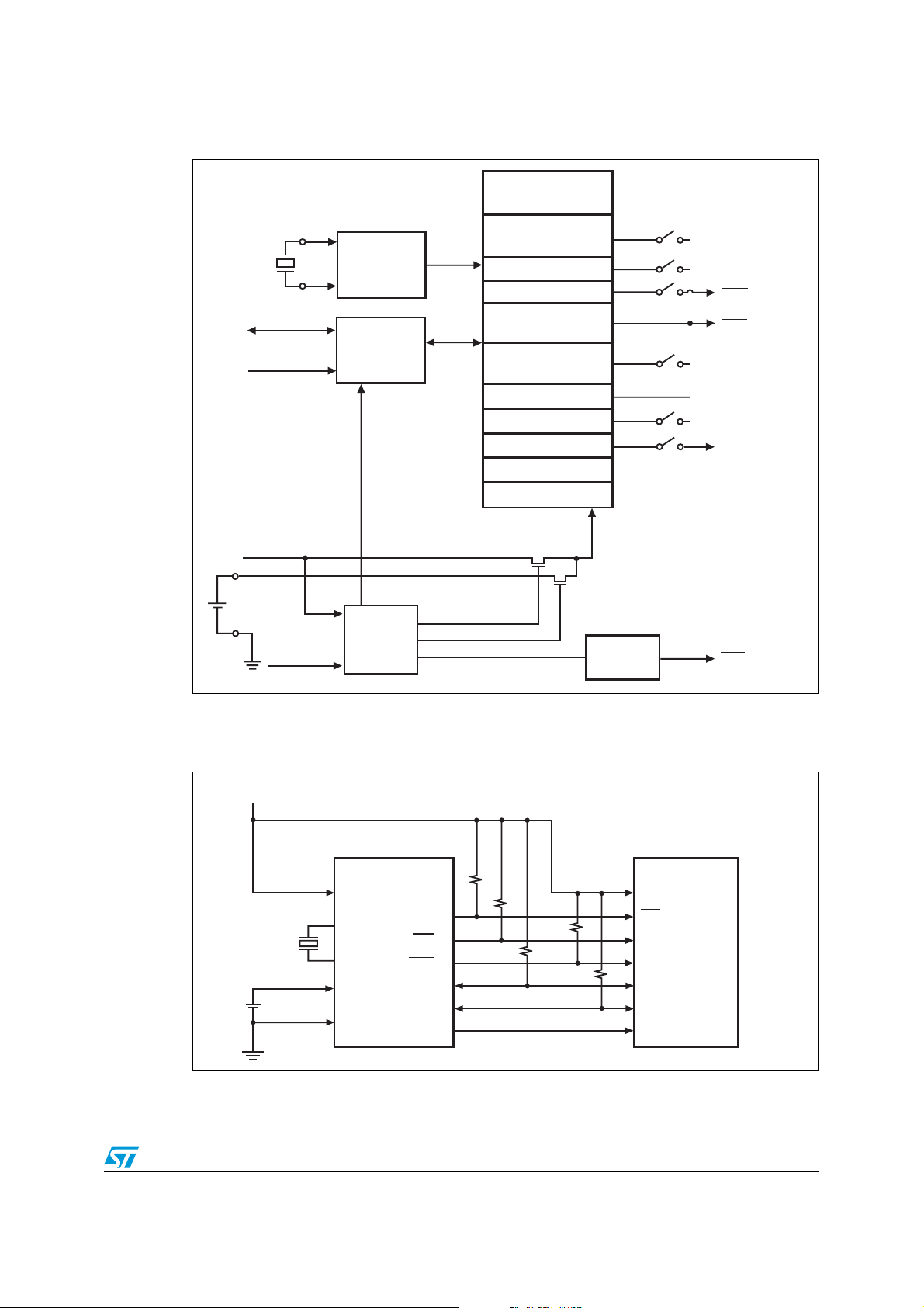
M41T82-M41T83 Description
Figure 8. M41T83 block diagram
REAL TIME CLOCK
CALENDAR
CRYSTAL
SDA
SCL
V
CC
V
BAT
V
RST/VSO
XI
OSCILLATOR
XO
INTERFACE
COMPARE
(2)
32KHz
I2C
WRITE
PROTECT
VCC < V
RST
OSCILLATOR FAIL
CIRCUIT
ALARM1
ALARM2
WATCHDOG
FREQUENCY TEST
OUTPUT DRIVER
8-BIT COUNTER
SQUARE WAVE
8 BITS OF OTP
USER SRAM (7 Bytes)
OFIE
A1IE
A2IE
FT
OUT
TIE
SQWE
INTERNAL
POWER
t
rec
TIMER
(1)
IRQ2
IRQ1/FT/OUT
SQW
(1)
RST
AI11800
(1)
1. Open drain output.
2. V
= VSO = 2.93 V (S), 2.63 V (R), and 2.32 V (Z).
RST
Figure 9. M41T83 hardware hookup
V
CC
M41T83
V
CC
RST
IRQ2
(1)
(1)
(1)
SCL
SDA
SQW
1. Open drain output.
IRQ1/FT/OUT
XI
XO
V
BAT
V
SS
MCU
V
CC
INT
Reset Input
Por t
Serial Clock Line
Serial Data Line
32KHz CLKIN
AI11801
Doc ID 12578 Rev 14 11/63
Page 12

Operation M41T82-M41T83
2 Operation
The M41T8x clock operates as a slave device on the serial bus. Access is obtained by
implementing a start condition followed by the correct slave address (D0h). The 32 bytes
contained in the device can then be accessed sequentially in the following order:
st
● 1
● 2
● 3
● 4
● 5
● 6
● 7
● 8
● 9
● 10
● 11
● 16
● 17
● 18
● 19
● 20
● 21
● 26
byte: tenths/hundredths of a second register
nd
byte: seconds register
rd
byte: minutes register
th
byte: century/hours register
th
byte: day register
th
byte: date register
th
byte: month register
th
byte: year register
th
byte: digital calibration register
th
byte: watchdog register
th
- 15th bytes: alarm 1 registers
th
byte: flags register
th
byte: timer value register
th
byte: timer control register
th
byte: analog calibration register
th
byte: square wave register
st
- 25th bytes: alarm 2 registers
th
- 32nd bytes: user RAM
The M41T8x clock continually monitors V
fall below V
, the device terminates an access in progress and resets the device address
RST
for an out-of-tolerance condition. Should V
CC
CC
counter. Inputs to the device will not be recognized at this time to prevent erroneous data
from being written to the device from an out-of-tolerance system. The power input will also
be switched from the V
switchover voltage (V
attached battery supply. As system power returns and V
disconnected, and the power supply is switched to external V
pin to the battery when V
CC
=
V
SO
). At this time the clock registers will be maintained by the
RST
falls below the battery back-up
CC
rises above VSO, the battery is
CC
CC
.
12/63 Doc ID 12578 Rev 14
Page 13

M41T82-M41T83 Operation
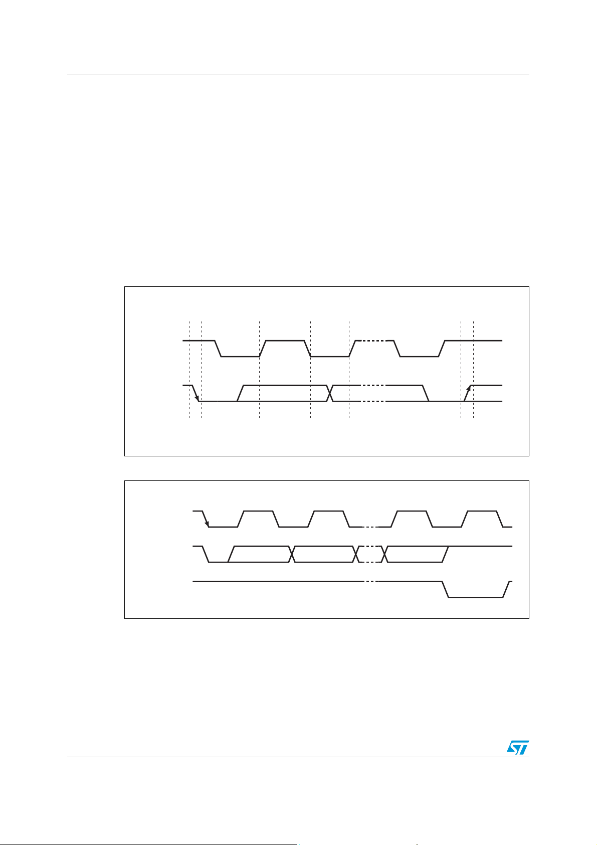
2.1 2-wire bus characteristics
The bus is intended for communication between different ICs. It consists of two lines: a bidirectional data signal (SDA) and a clock signal (SCL). Both the SDA and SCL lines must be
connected to a positive supply voltage via a pull-up resistor.
The following protocol has been defined:
● Data transfer may be initiated only when the bus is not busy.
● During data transfer, the data line must remain stable whenever the clock line is high.
● Changes in the data line, while the clock line is high, will be interpreted as control
signals.
Accordingly, the following bus conditions have been defined:
2.1.1 Bus not busy
Both data and clock lines remain high.
2.1.2 Start data transfer
A change in the state of the data line, from high to low, while the clock is high, defines the
START condition.
2.1.3 Stop data transfer
A change in the state of the data line, from low to high, while the clock is high, defines the
STOP condition.
2.1.4 Data valid
The state of the data line represents valid data when after a start condition, the data line is
stable for the duration of the high period of the clock signal. The data on the line may be
changed during the low period of the clock signal. There is one clock pulse per bit of data.
Each data transfer is initiated with a start condition and terminated with a stop condition.
The number of data bytes transferred between the start and stop conditions is not limited.
The information is transmitted byte-wide and each receiver acknowledges with a ninth bit.
By definition a device that gives out a message is called “transmitter,” the receiving device
that gets the message is called “receiver.” The device that controls the message is called
“master.” The devices that are controlled by the master are called “slaves.”
Doc ID 12578 Rev 14 13/63
Page 14
Operation M41T82-M41T83
2.1.5 Acknowledge
Each byte of eight bits is followed by one acknowledge bit. This acknowledge bit is a low
level put on the bus by the receiver whereas the master generates an extra acknowledge
related clock pulse. A slave receiver which is addressed is obliged to generate an
acknowledge after the reception of each byte that has been clocked out of the slave
transmitter.
The device that acknowledges has to pull down the SDA line during the acknowledge clock
pulse in such a way that the SDA line is a stable low during the high period of the
acknowledge related clock pulse. Of course, setup and hold times must be taken into
account. A master receiver must signal an end of data to the slave transmitter by not
generating an acknowledge on the last byte that has been clocked out of the slave. In this
case the transmitter must leave the data line high to enable the master to generate the
STOP condition.
Figure 10. Serial bus data transfer sequence
DATA LINE
STABLE
DATA VALID
CLOCK
DATA
STA RT
CONDITION
CHANGE OF
DATA ALLOWED
Figure 11. Acknowledgement sequence
STA RT
SCL FROM
MASTER
DATA OUTPUT
BY TRANSMITTER
DATA OUTPUT
BY RECEIVER
12 8 9
MSBLSB
STOP
CONDITION
AI00587
CLOCK PULSE FOR
ACKNOWLEDGEMENT
AI00601
14/63 Doc ID 12578 Rev 14
Page 15
M41T82-M41T83 Operation
2.2 Read mode
In this mode the master reads the M41T8x slave after setting the slave address (see
Figure 13 on page 16). Following the WRITE mode control bit (R/W = 0) and the
acknowledge bit, the word address 'An' is written to the on-chip address pointer. Next the
START condition and slave address are repeated followed by the READ mode control bit
(R/W = 1). At this point the master transmitter becomes the master receiver. The data byte
which was addressed will be transmitted and the master receiver will send an acknowledge
bit to the slave transmitter. The address pointer is only incremented on reception of an
acknowledge clock. The M41T8x slave transmitter will now place the data byte at address
An+1 on the bus, the master receiver reads and acknowledges the new byte and the
address pointer is incremented to An+2.
This cycle of reading consecutive addresses will continue until the master receiver sends a
STOP condition to the slave transmitter. Most of the registers and memory locations are
accessed directly, but the RTC counters are accessed via a set of buffer/transfer registers at
addresses 00h to 07h. The counters are not directly read nor written. Instead, at the start of
a read or write cycle, the counters are copied into the eight buffer/transfer registers so that
the user can read them out sequentially, receiving a coherent set of data, copied from the
same instant in time.
An alternate READ mode may also be implemented whereby the master reads the M41T8x
slave without first writing to the (volatile) address pointer. The first address that is read is the
last one stored in the pointer (see Figure 14 on page 16).
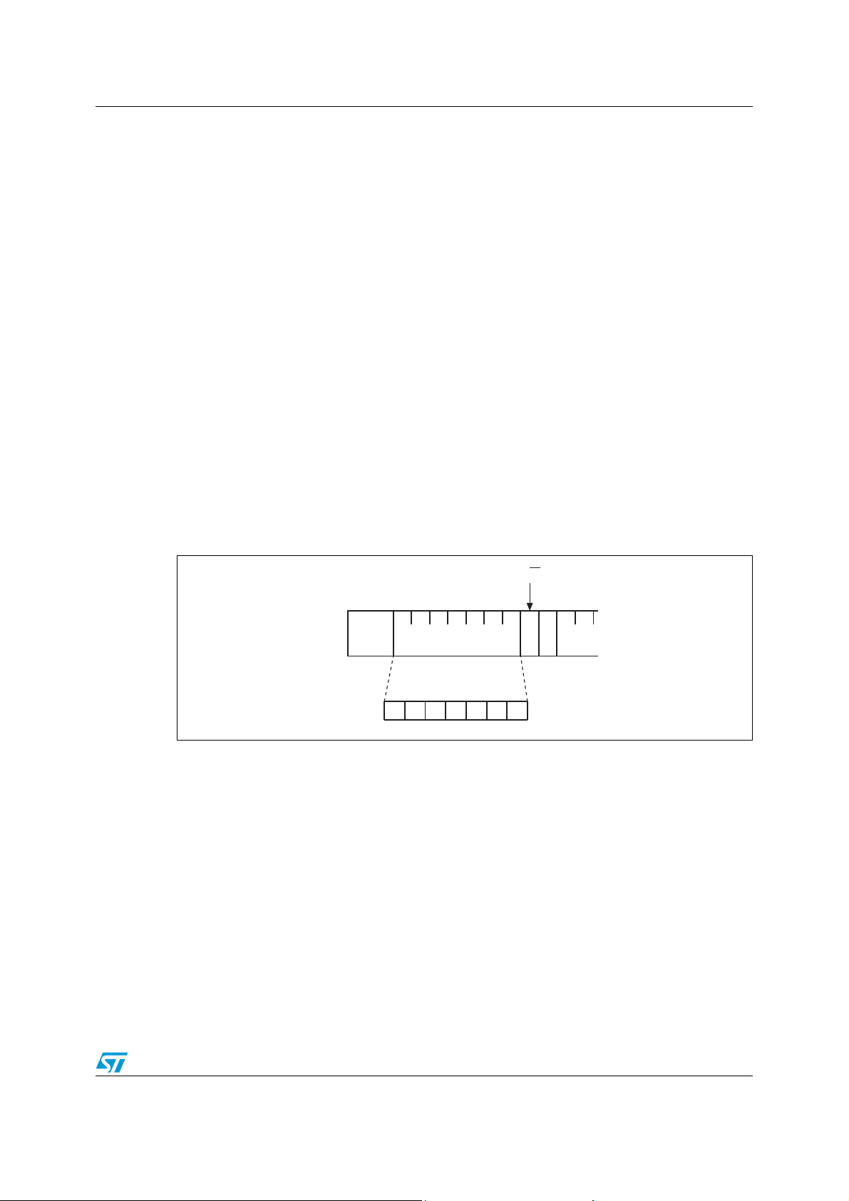
Figure 12. Slave address location
STA RT A
SLAVE ADDRESS
MSB
0100 011
R/W
LSB
AI00602
Doc ID 12578 Rev 14 15/63
Page 16
Operation M41T82-M41T83
Figure 13. Read mode sequence
BUS ACTIVITY:
MASTER
SDA LINE
BUS ACTIVITY:
STA RT
S
SLAVE
ADDRESS
R/W
ADDRESS (An)
ACK
DATA n+X
WORD
STOP
P
NO ACK
Figure 14. Alternative read mode sequence
BUS ACTIVITY:
MASTER
STA RT
R/W
STA RT
S
ACK
ADDRESS
SLAVE
R/W
DATA n DATA n+ 1
ACK
ACK
ACK
AI00899
STOP
BUS ACTIVITY:
S
SLAVE
ADDRESS
DATA n DATA n+ 1 DATA n+ X
ACK
ACK
ACK
ACK
PSDA LINE
NO ACK
AI00895
16/63 Doc ID 12578 Rev 14
Page 17
M41T82-M41T83 Operation
2.3 Write mode
In this mode the master transmitter transmits to the M41T8x slave receiver. Bus protocol is
shown in Figure 15. Following the START condition and slave address, a logic 0 (R/W = 0) is
placed on the bus and indicates to the addressed device that word address “An” will follow
and is to be written to the on-chip address pointer. The data word to be written to the
memory is strobed in next and the internal address pointer is incremented to the next
address location on the reception of an acknowledge clock. The M41T8x slave receiver will
send an acknowledge clock to the master transmitter after it has received the slave address
see Figure 12 on page 15 and again after it has received the word address and each data
byte.
Figure 15. Write mode sequence
BUS ACTIVITY:
MASTER
BUS ACTIVITY:
As in the case of reading, some registers and memory locations are written directly, but the
RTC counters are written via a set of eight buffer/transfer registers at addresses 00h to 07h.
The user will write the date and time information sequentially, and then, at the end of the I
write cycle or when the address pointer increments beyond 07h, the buffer/transfer registers
will be copied into the RTC counters. All the time parameters - fractions, seconds, minutes,
hours, day, date, month, year, and century bits - are copied simultaneously.
Whatever value is in the buffer/transfer registers will be copied to the counters, so if the user
only changes one of the eight bytes, the remaining seven bytes will receive the unchanged
contents of the buffer/transfer registers, which will contain whatever was in the counters at
the start of the write access.
For example, if the user starts a write cycle on Monday, November 16, 2009, at 17:52:27.03,
and writes a 22 to the minutes registers, the value Monday, November 16, 2009,
17:52:22.03 will be written back into the counters. At the start of the write cycle, the eight
bytes of counters were copied into the buffer/transfer registers. Then, the seconds register
was overwritten. Finally, the eight bytes were copied back into the counters with the result
that the seconds value was changed.
STA RT
S
ADDRESS
SLAVE
R/W
WORD
ADDRESS (An)
ACK
DATA n DATA n+1 DATA n+X
ACK
ACK
ACK
PSDA LINE
ACK
STOP
AI00591
2
C
Doc ID 12578 Rev 14 17/63
Page 18

Operation M41T82-M41T83
2.4 Data retention and battery switchover (VSO = V
Once VCC falls below the switchover voltage (VSO = V
switches over to the battery and powers down into an ultra low current mode of operation to
preserve battery life. If V
from V
CC
to V
when VCC drops below V
BAT
clock registers and user RAM will be maintained by the attached battery supply.
When it is powered back up, the device switches back from battery to V
hysteresis. When V
rises above V
CC
on battery storage life refer to Application Note AN1012.
2.5 Power-on reset (t
The M41T8x continuously monitors VCC. When VCC falls to the power fail detect trip point,
the RST
typical) after V
Note: The t
below V
RST
The RST
chosen to control the rise time.
output pulls low (open drain) and remains low after power-up for t
rises above V
CC
period does not affect the RTC operation. Write protect only occurs when VCC is
rec
. When VCC rises above V
RST
output is affected by the t
pin is an open drain output and an appropriate pull-up resistor to VCC should be
is less than, or greater than V
BAT
rec
)
RST
rec
RST
(max).
RST
period.
(see Figure 27 on page 52). At this time the
RST
, it will recognize the inputs. For more information
, the RTC will be selectable immediately. Only the
), the device automatically
RST
, the device power is switched
RST
RST
at VSO +
CC
rec
)
(210 ms
18/63 Doc ID 12578 Rev 14
Page 19

M41T82-M41T83 Clock operation
3 Clock operation
The M41T8x is driven by a quartz-controlled oscillator with a nominal frequency of
32.768 kHz. The accuracy of the real-time clock depends on the frequency of the quartz
crystal that is used as the time-base for the RTC.
The 8-byte clock register (see Table 2 on page 23 and Table 4 on page 25) is used to both
set the clock and to read the date and time from the clock, in binary coded decimal format.
Tenths/hundredths of seconds, seconds, minutes, and hours are contained within the first
four registers.
Bit D7 of register 01h contains the STOP bit (ST). Setting this bit to a '1' will cause the
oscillator to stop. When reset to a 0 the oscillator restarts within one second (typical).
Note: Upon initial power-up, the user should set the ST bit to a '1,' then immediately reset the ST
bit to 0. This provides an additional “kick-start” to the oscillator circuit.
Bits D6 and D7 of clock register 03h (century/ hours register) contain the CENTURY bit 0
(CB0) and CENTURY bit 1 (CB1). Bits D0 through D2 of register 04h contain the day (day of
week). Registers 05h, 06h, and 07h contain the date (day of month), month, and years. The
ninth clock register is the digital calibration register, while the analog calibration register is
found at address 12h (these are both described in Section 3.4: Clock calibration). The RTC
includes an oscillator fail detect circuit which sets the OF bit in the flags register (bit 2,
register 0fh). For the M41T83, bit D7 of register 09h (watchdog register) contains the
oscillator fail interrupt enable bit (OFIE) which can be used to enable an interrupt when the
OF bit is set (see Section 3.12: Oscillator fail detection on page 42) will also generate an
interrupt output.
Note: A WRITE to ANY location within the first eight bytes of the clock register (00h-07h),
including the ST bit and CB0-CB1 bits will result in an update of the RTC counters and a
reset of the divider chain. This could result in an inadvertent change of the current time. For
example, the ST bit is in the seconds register (address 01h) and the century bits (CB0-CB1)
are in the hours register (address 03h), so the user should take care to not alter these other
parameters when changing the ST bit or the century bits.
The eight clock registers may be read one byte at a time or in a sequential block. At the start
of a read cycle, a copy of the time/date counters is placed in the buffer/transfer registers and
can then be transferred out sequentially without concern that the time/date increments
during the transfer and thus yields a corrupt value. For example, if the user were to read the
seconds register, then start another bus cycle to read the minutes register, the minutes
counter could have incremented during the time between the two read cycles. The seconds
and minutes values would not be from the same instant in time; they would not be coherent.
By using the sequential read feature, the values shifted out are from the same instant in time
and are thus coherent.
Similarly, when writing to the RTC registers, during one write cycle, the user can
sequentially transfer all eight bytes of time/date into the buffer/transfer registers whereupon
they will be loaded simultaneously into the RTC counters thus ensuring a coherent update
of the time/date.
Doc ID 12578 Rev 14 19/63
Page 20

Clock operation M41T82-M41T83
3.1 Clock data coherency
In order to synchronize the data during reads and writes of the real-time clock device, a set
of buffer transfer registers resides between the I
clock/calendar counters in the part. While the read/write data is transferred in and out of the
device one bit at a time to the user, the transfers between the buffer registers and counters
occur such that all the bits are copied simultaneously. This keeps the data coherent and
ensures that none of the counters are incremented while the data is being transferred.
Figure 16. Clock data coherency
AT START OF READ OR WRITE,
DATA IN COUNTERS IS COPIED TO
BUFFER/TRANSFER REGISTERS.
READ / WRITE
BUFFER-TRANSFER
REGISTERS
I2C
2
I2C
INTERFACE
SECONDS
MINUTES
HOURS
DAY-OF-WEEK
DATE
MONTHS
YEARS
CENTURIES
2
C serial interface on the user side, and the
32KHz
OSC
DIVIDE BY 32768
1 Hz
COUNTER
COUNTER
COUNTER
COUNTER
COUNTER
COUNTER
COUNTER
RTC
COUNTERS
COUNTER
NON-CLOCK
REGISTERS
SQUAREWAVE
CALIBRATION
ALARM / HALT
WATCHDOG
3.1.1 Example of incoherency
Without having the intervening buffer/transfer registers, if the user began directly reading the
counters at 23:59:59, a read of the seconds register would return 59 seconds. After the
address pointer incremented, the next read would return 59 minutes. Then the next read
should return 23 hours, but if the clock happened to increment between the reads, the user
would see 00 hours. When the time was re-assembled, it would appear as 00:59:59, and
thus be incorrect by one hour.
By using the buffer/transfer registers to hold a copy of the time, the user is able to read the
entire set of registers without any values changing during the read.
Similarly, when the application needs to change the time in the counters, it is necessary that
all the counters be loaded simultaneously. Thus, the user writes sequentially to the various
buffer/transfer registers, then they are copied to the counters in a single transfer thereby
coherently loading the counters.
AFTER A WRITE, DATA IS TRANSFERRED
FROM BUFFERS TO COUNTERS
HALT BIT SET AT POWER-DOWN
20/63 Doc ID 12578 Rev 14
Page 21

M41T82-M41T83 Clock operation
3.1.2 Accessing the device
The M41T82/83 is comprised of 32 addresses which provide access to registers for time
and date, digital and analog calibration, two alarms, watchdog, flags, timer, squarewave
(M41T83 only) and NVRAM. The clock and alarm parameters are in binary coded decimal
(BCD) format. The calibration, timer, watchdog, and squarewave parameters are in a binary
format.
In the case of the M41T82 and M41T83, at the start of each read or write serial transfer, the
counters are automatically copied to the buffer registers. In the event of a write to any
register in the range 0-7, at the end of the serial transfer, the buffer registers are copied back
into the counters thus revising the date/time. Any of the eight clock registers (addresses 0-
7) not updated during the transfer will have its old value written back into the counters. For
example, if only the seconds value is revised, the other seven counters will end up with the
same values they had at the start of the serial transfer.
However, writes which do not affect the clock registers - that is, a write only to the non-clock
registers (addresses 0x08 to 0x1F) - will not cause the buffer registers to be copied back to
the counters. The counters are only updated if a register in the range 0-7 was written.
Whenever the RTC registers (addresses 0-7) are written, the divider chain from the
oscillator is reset.
3.2 Halt bit (HT) operation
When the part is powered down into battery backup mode, a control bit, called the Halt or
HT bit, is set automatically. This inhibits any subsequent transfers from the counters to the
buffer registers thereby freezing in the buffer registers the time/date of the last access of the
part.
Repeated reads of the clock registers will return the same value. After the HT bit is cleared,
by writing bit 6 of address 0x0C to 0, the next read of the RTC will return the present time.
Note: Writes to the RTC registers (addresses 0-7) with the HT bit set can cause time corruption.
Since the buffer registers contain the time of the last access prior to the HT bit being set, any
write in the address range 0-7 will result in the time of the last access being copied back into
the counters.
Example: The last access was November 17, 2009, at 16:15:07.77. The system later
powered down thus setting the HT bit and freezing that value in the buffers. Later, on
December 18, 2009, at 03:22:43.35, the system is powered up and the user writes the
seconds to 46 without first clearing the HT bit. At the end of the serial transfer, the old
time/date, with the seconds modified to 46, will be written back into the clock registers
thereby corrupting them. The new, wrong time will be November 17, 2009, at 16:15:46.77.
This makes it appear the RTC lost time during the power outage.
Thus, at power-up, the user should always clear the HT bit (write bit 6 to 0 at address 0x0C)
before writing to any address in the range 0-7.
A typical power-up flow is to read the time of last access, then clear the HT bit, then read the
current time.
Doc ID 12578 Rev 14 21/63
Page 22

Clock operation M41T82-M41T83
3.2.1 Power-down time-stamp
Some applications may need to determine the amount of time spent in backup mode. That
can be calculated if the time of power-down and the time of power-up are known. The latter
is straightforward to obtain. But the time of power-down is only available if an access
occurred just prior to power-down. That is, if there was an access of the device just prior to
power-down, the time of the access would have been frozen in the buffer transfer registers
and thus the approximate time of power-down could be obtained.
If an application requires the time of power-down, the best way to implement it is to set up
the software to do frequent reads of the clock, such as once every 1 or 5 seconds. That
way, at power-up, the buffer-transfer registers will contain a time value within 1 (or 5)
seconds of the actual time of power-down. For more information, please refer to AN1572,
“Power-down time-stamp function in serial real-time clocks (RTCs)”.
22/63 Doc ID 12578 Rev 14
Page 23

M41T82-M41T83 Clock operation
Table 2. M41T82 clock/control register map (32 bytes)
Addr
D7 D6 D5 D4 D3 D2 D1 D0
(1)
Function/range BCD
format
00h 0.1 seconds 0.01 seconds seconds 00-99
01h ST 10 seconds seconds seconds 00-59
02h 0 10 minutes minutes minutes 00-59
03h CB1 CB0 10 hours Hours (24 hour format) Century/hours 0-3/00-23
04h 0 0 0 0 0 Day of week Day 01-7
05h 0 0 10 date Date: day of month Date 01-31
06h 0 0 0 10M Month Month 01-12
07h 10 years Year Year 00-99
08h 0 FT DCS DC4 DC3 DC2 DC1 DC0 Digital calibration
09h 0 BMB4 BMB3 BMB2 BMB1 BMB0 RB1 RB0 Watchdog
0Ah 0 0 ABE Al1 10M Alarm1 month Al1 month 01-12
0Bh RPT14 RPT15 AI1 10 date Alarm1 date Al1 date 01-31
0Ch RPT13 HT AI1 10 hour Alarm1 hour Al1 hour 00-23
0Dh RPT12 Alarm1 10 minutes Alarm1 minutes Al1 min 00-59
0Eh RPT11 Alarm1 10 seconds Alarm1 seconds Al1 sec 00-59
(2)
0Fh WDF AF1 AF2
BL TF OF 0 0 Flags
10h Timer countdown value Timer value
11h TE 0 0 0 0 0 TD1 TD0 Timer control
12h ACS AC6 AC5 AC4 AC3 AC2 AC1 AC0 Analog calibration
13h 0 0 0 0 0 0 AL2E 0 SQW
14h 0
(3)
(3)
0
(3)
0
Al2 10M Alarm2 month SRAM/Al2 month 01-12
15h RPT24 RPT25 AI2 10 date Alarm2 month SRAM/Al2 date 01-31
16h RPT23 0
(3)
AI2 10 hour Alarm2 date SRAM/Al2 hour 00-23
17h RPT22 Alarm2 10 minutes Alarm2 minutes SRAM/Al2 min 00-59
18h RPT21 Alarm2 10 seconds Alarm2 seconds SRAM/Al2 sec 00-59
19h-1Fh User SRAM (7 bytes) SRAM
1. See Table 3: Key to Table 2: M41T82 clock/control register map (32 bytes)
2. AF2 will always read 0, if the AL2E bit is set to 0.
3. As indicated in Table 3, the 0 bits should be written to 0. But in the case of these four bits, when AL2E is 0, registers 14-18h
are SRAM locations and these bits become SRAM cells which are thus excluded from that restriction.
Doc ID 12578 Rev 14 23/63
Page 24

Clock operation M41T82-M41T83
Table 3. Key to Table 2: M41T82 clock/control register map (32 bytes)
Code Explanation
0 Must be set to zero
ABE Alarm in battery backup enable bit
AC0-AC6 Analog calibration bits
ACS Analog calibration sign bit
AF1, AF2 Alarm flag bits
AL2E Alarm 2 enable bit
BL Battery low bit
BMB0-BMB4 Watchdog multiplier bits
CB0, CB1 Century bits
DC0-DC4 Digital calibration bits
DCS Digital calibration sign bit
FT Frequency test bit
HT Halt update bit
OF Oscillator fail bit
RB0-RB2 Watchdog resolution bits
RPT11-RPT15 Alarm 1 repeat mode bits
RPT21-RPT25 Alarm 2 repeat mode bits
ST Stop bit
TD0, TD1 Timer frequency bits
TE Timer enable bit
TF Timer flag
WDF Watchdog flag
24/63 Doc ID 12578 Rev 14
Page 25

M41T82-M41T83 Clock operation
Table 4. M41T83 clock/control register map (32 bytes)
Addr
D7 D6 D5 D4 D3 D2 D1 D0
(1)
Function/range BCD
format
00h 0.1 seconds 0.01 seconds seconds 00-99
01h ST 10 seconds seconds seconds 00-59
02h 0 10 minutes Minutes Minutes 00-59
03h CB1 CB0 10 hours Hours (24 hour format) Century/hours 0-3/00-23
04h 0 0 0 0 0 Day of week Day 01-7
05h 0 0 10 date Date: day of month Date 01-31
06h 0 0 0 10M Month Month 01-12
07h 10 years Year Year 00-99
08h OUT FT DCS DC4 DC3 DC2 DC1 DC0 Digital calibration
09h OFIE BMB4 BMB3 BMB2 BMB1 BMB0 RB1 RB0 Watchdog
0Ah A1IE SQWE ABE
Al1
10M
Alarm 1month Al1 month 01-12
0Bh RPT14 RPT15 AI1 10 date Alarm1 date Al1 date 01-31
0Ch RPT13 HT AI1 10 hour Alarm1 hour Al1 hour 00-23
0Dh RPT12 Alarm1 10 minutes Alarm1 minutes Al1 min 00-59
0Eh RPT11 Alarm1 10 seconds Alarm1 seconds Al1 sec 00-59
(2)
0Fh WDF AF1 AF2
BL TF OF 0 0 Flags
10h Timer countdown value Timer value
11h TE TI/TP TIE 0 0 0 TD1 TD0 Timer control
12h ACS AC6 AC5 AC4 AC3 AC2 AC1 AC0
Analog
calibration
13h RS3 RS2 RS1 RS0 0 0 AL2E OTP SQW
14h A2IE 0
(3)
(3)
0
Al2
10M
Alarm2 month SRAM/Al2 month 01-12
15h RPT24 RPT25 AI2 10 date Alarm2 date SRAM/Al2 date 01-31
16h RPT23 0
(3)
AI2 10 hour Alarm2 hour SRAM/Al2 hour 00-23
17h RPT22 Alarm2 10 minutes Alarm2 minutes SRAM/Al2 min 00-59
18h RPT21 Alarm2 10 seconds Alarm2 seconds SRAM/Al2 sec 00-59
19h-
1Fh
1. See Table 5: Key to Table 4: M41T83 clock/control register map (32 bytes).
2. AF2 will always read 0, if the AL2E bit is set to 0.
3. As indicated in Table 5, the 0 bits should be written to 0. But in the case of these three bits, when AL2E is 0, registers
14-18h are SRAM locations and these bits become SRAM cells which are thus excluded from that restriction.
User SRAM (7 bytes) SRAM
Doc ID 12578 Rev 14 25/63
Page 26

Clock operation M41T82-M41T83
Table 5. Key to Table 4: M41T83 clock/control register map (32 bytes)
Code Explanation
0 Must be set to zero
ABE Alarm in battery back-up enable bit
A1IE, A2IE Alarm interrupt enable bits
AC0-AC6 Analog calibration bits
ACS Analog calibration sign bit
AF1, AF2 Alarm flag
AL2E Alarm 2 enable bit
BL Battery low bit
BMB0-BMB4 Watchdog multiplier bits
CB0, CB1 Century bits
DC0-DC4 Digital calibration bits
DCS Digital calibration Sign bit
FT Frequency test bit
HT Halt update bit
OF Oscillator fail bit
OUT Output level
OFIE Oscillator fail interrupt enable
OTP OTP control bit
RB0-RB2 Watchdog resolution bits
RPT11-RPT15 Alarm 1 repeat mode bits
RPT21-RPT25 Alarm 2 repeat mode bits
RS0-RS3 SQW frequency
SQWE Square wave enable
SRAM/ALM2
SRAM/alarm 2 bit
ST Stop bit
TD0, TD1 Timer frequency bits
TE Timer enable bit
TF Timer flag
/TP Timer interrupt or pulse
TI
TIE Timer interrupt enable
WDF Watchdog flag
26/63 Doc ID 12578 Rev 14
Page 27

M41T82-M41T83 Clock operation
3.3 Real-time clock accuracy
The M41T8x is driven by a quartz controlled oscillator with a nominal frequency of
32,768 Hz. The accuracy of the real-time clock is dependent upon the accuracy of the
crystal, and the match between the capacitive load of the oscillator circuit and the capacitive
load for which the crystal was trimmed. Temperature also affects the crystal frequency,
causing additional error (see Figure 18 on page 32).
The M41T8x provides the option of clock correction through either manufacturing calibration
or in-application calibration. The total possible compensation is typically –93 ppm to +156
ppm. The two compensation circuits that are available are:
1. An analog calibration register (12h) can be used to adjust internal (on-chip) load
capacitors for oscillator capacitance trimming. The individual load capacitors C
C
(see Figure 17), are selectable from a range of –18 pF to +9.75 pF in steps of
XO
0.25 pF. This translates to a calculated compensation of approximately ±30 ppm (see
Section 3.4.2: Analog calibration (programmable load capacitance) on page 31).
2. A digital calibration register (08h) can also be used to adjust the clock counter by
adding or subtracting a pulse at the 512 Hz divider stage. This approach provides
periodic compensation of approximately –63 ppm to +126 ppm (see Section 3.4.1:
Digital calibration (periodic counter correction) on page 28).
Figure 17. Internal load capacitance adjustment
XI
and
XI
XO
C
XI
Crystal Oscillator
C
XO
AI11804
Doc ID 12578 Rev 14 27/63
Page 28

Clock operation M41T82-M41T83
3.4 Clock calibration
The M41T8x oscillator is designed for use with a 12.5 pF crystal load capacitance. When
the calibration circuit is properly employed, accuracy improves to better than ±1 ppm at
25 °C.
The M41T8x design provides the following two methods for clock error correction.
3.4.1 Digital calibration (periodic counter correction)
This method employs the use of periodic counter correction by adjusting the ratio of the
100 Hz divider stage to the 512 Hz divider stage. Under normal operation, the 100 Hz
divider stage outputs precisely 100 pulses for every 512 pulses of the 512 Hz input stage to
provide the input frequency to the fraction of seconds clock register. By adjusting the
number of 512 Hz input pulses used to generate 100 output pulses, the clock can be sped
up or slowed down, as shown in Figure 20 on page 34.
When a non-zero value is loaded into the five calibration bits (DC4 – DC0) found in the
digital calibration register (08h) and the sign bit is 1, (indicating positive calibration), the
100 Hz stage outputs 100 pulses for every 511 input pulses instead of the normal 512.
Since the 100 pulses are now being output in a shorter window, this has the effect of
speeding up the clock by 1/512 seconds for each second the circuit is active. Similarly, when
the sign bit is 0, indicating negative calibration, the block outputs 100 pulses for every 513
input pulses. Since the 100 pulses are then being output in a longer window, this has the
effect of slowing down the clock by 1/512 seconds for each second the circuit is active.
The amount of calibration is controlled by using the value in the calibration register (N) to
generate the adjustment in one second increments. This is done for the first N seconds once
every eight minutes for positive calibration, and for N seconds once every sixteen minutes
for negative calibration (see Table 6 on page 30).
For example, if the calibration register is set to 100010, then the adjustment will occur for
two seconds in every minute. Similarly, if the calibration register is set to 000011, then the
adjustment will occur for 3 seconds in every alternating minute.
The digital calibration bits (DC4 – DC0) occupy the five lower order bits in the digital
calibration register (08h). These bits can be set to represent any value between 0 and 31 in
binary form. The sixth bit (DCS) is a sign bit; 1 indicates positive calibration, 0 indicates
negative calibration. Calibration occurs within an 8-minute (positive) or 16-minute (negative)
cycle. Therefore, each calibration step has an effect on clock accuracy of +4.068 or –2.034
ppm. Assuming that the oscillator is running at exactly 32,768 Hz, each of the 31 increments
in the calibration byte would represent +10.7 or –5.35 seconds per month, which
corresponds to a total range of +5.5 or –2.75 minutes per month.
One method of determining the amount of digital calibration required is to use the frequency
test output (FT) of the device (see Section 3.14: IRQ1/FT/OUT pin, frequency test,
interrupts and the OUT bit (M41T83 only) on page 43 for more information on enabling the
FT output).
When FT is enabled, a 512 Hz signal is output in the IRQ1
on the FT/RST
timing device such as a frequency counter. The measured value is then compared to 512 Hz
and the oscillator error in ppm is then determined.
pin on the M41T82. This signal can be measured using a highly accurate
/FT/OUT pin on the M41T83, and
The user should keep in mind that changes in the digital calibration value will not affect the
signal measured on the FT pin. While the analog calibration circuit does affect the oscillator,
28/63 Doc ID 12578 Rev 14
Page 29

M41T82-M41T83 Clock operation
the digital calibration circuitry uses periodic counter correction which occurs downstream of
the 512 Hz divider chain and hence has no effect on the FT pin.
Note: 1 The modified pulses are not observable on the frequency test (FT) output, nor will the effect
of the calibration be measurable real-time, due to the periodic nature of the error
compensation.
2 Positive digital calibration is performed on an eight minute cycle, therefore the value in the
calibration register should not be modified more frequently than once every eight minutes for
positive values of calibration. Negative digital calibration is performed on a sixteen minute
cycle, therefore negative values in the calibration register should not be modified more
frequently than once every sixteen minutes.
Doc ID 12578 Rev 14 29/63
Page 30

Clock operation M41T82-M41T83
Table 6. Digital calibration values
Calibration value (binary) Calibration value rounded to the nearest ppm
DC4 – DC0
Negative calibration (DCS = 0)
to slow a fast clock
Positive calibration (DCS = 1)
to speed up a slow clock
0 (00000) 0 0
1 (00001) –2 4
2 (00010) –4 8
3 (00011) –6 12
4 (00100) –8 16
5 (00101) –10 20
6 (00110) –12 24
7 (00111) –14 28
8 (01000) –16 33
9 (01001) –18 37
10 (01010) –20 41
11 (01011) –22 45
12 (01100) –24 49
13 (01101) –26 53
14 (01110) –28 57
15 (01111) –31 61
16 (10000) –33 65
17 (10001) –35 69
18 (10010) –37 73
19 (10011) –39 77
20 (10100) –41 81
21 (10101) –43 85
22 (10110) –45 90
23 (10111) –47 94
24 (11000) –49 98
25 (11001) –51 102
26 (11010) –53 106
27 (11011) –55 110
28 (11100) –57 114
29 (11101) –59 118
30 (11110) –61 122
31 (11111) –63 126
N N/491520 (per minute) N/245760 (per minute)
30/63 Doc ID 12578 Rev 14
Page 31

M41T82-M41T83 Clock operation
3.4.2 Analog calibration (programmable load capacitance)
A second method of calibration employs the use of programmable internal load capacitors to
adjust (or trim) the oscillator frequency. As discussed in Section 3.4.1, the 512 Hz frequency
test output can be used to determine the amount of frequency error in the oscillator.
Changes in the analog calibration value will affect the frequency test output, thus the user
can immediately see the effects of these changes (see Section 3.14 on page 43 for more
information on enabling the FT output).
By design, the oscillator is intended to be 0 ppm ± crystal accuracy at room temperature
(25 °C, see Figure 18 on page 32). For a 12.5 pF crystal, the default loading on each side of
the crystal will be 25 pF. For incrementing or decrementing the calibration value,
capacitance will be added or removed in increments of 0.25 pF to each side of the crystal.
Internally, C
C
, connected from the XI and XO pins to ground (see Figure 17 on page 27). The
XO
effective on-chip series load capacitance, C
of the oscillator is changed via two digitally controlled capacitors, CXI and
LOAD
, ranges from 3.5 pF to 17.4 pF, with a
LOAD
nominal value of 12.5 pF (AC0 – AC6 = 0).
The effective series load capacitance (C
C
LOAD
) is the combination of CXI and CXO:
LOAD
11C
⁄ 1CXO⁄+()⁄=
XI
Seven analog calibration bits, AC0 to AC6, are provided in order to adjust the on-chip load
capacitance value for frequency compensation of the RTC. Each bit has a different weight
for capacitance adjustment. An analog calibration sign (ACS) bit determines if capacitance
is added (ACS bit = 0, negative calibration) or removed (ACS bit = 1, positive calibration).
The majority of the calibration adjustment is positive (i.e. to increase the oscillator frequency
by removing capacitance) due to the typical characteristic of quartz crystals to slow down
due to changes in temperature, but negative calibration is also available.
Since the analog calibration register adjustment is essentially pulling the frequency of the
oscillator, the resulting frequency changes will not be linear with incremental capacitance
changes. The equations which govern this mechanism indicate that smaller capacitor values
of analog calibration adjustment will provide larger increments. Thus, the larger values of
analog calibration adjustment will produce smaller incremental frequency changes. These
values typically vary from 6-10 ppm/bit at the low end to <1 ppm/bit at the highest
capacitance settings. The range provided by the analog calibration register adjustment with
a typical surface mount crystal is approximately ±30 ppm around the AC6-AC0 = 0 default
setting because of this property (see Table 7 on page 32).
Pre-programmed calibration value
Users of the M41T83 in the embedded crystal package have the option of using the factory
programmed analog calibration value (refer to Section 3.17: OTP bit operation (M41T83 in
SOX18 package only) on page 47).
Doc ID 12578 Rev 14 31/63
Page 32

Clock operation M41T82-M41T83
Figure 18. Crystal accuracy across temperature
Frequency (ppm)
20
0
–20
–40
–60
2
)
O
= 25°C ± 5°C
T
O
2
80–10–20–30–40
AI07888
–80
–100
–120
–140
–160
ΔF
= K x (T – T
F
= –0.036 ppm/°C2 ± 0.006 ppm/°C
K
010203040506070
Temperature °C
Table 7. Analog calibration values
Analog
Addr
calibration
value
D7 D6 D5 D4 D3 D2 D1 D0 C
ACS
(±)
AC6
(16 pF)
AC5
(8 pF)
0 pF x 0 0 0 0 0 0 0 25 pF 12.5 pF
3 pF 0 0 0 0 1 1 0 0 28 pF 14 pF
5 pF 0 0 0 1 0 1 0 0 30 pF 15 pF
12h
–7 pF 1 0 0 1 1 1 0 0 18 pF 9 pF
9.75 pF
1. C
LOAD
2. Maximum negative calibration value.
3. Maximum positive calibration value.
(2)
0 0 1 0 0 1 1 1 34.75 pF 17.4 pF
(3)
–18 pF
= 1/(1/CXI + 1/CXO).
1 1 0 0 1 0 0 0 7 pF 3.5 pF
AC4
(4 pF)
AC3
(2 pF)
AC2
(1 pF)
AC1
(0.5 pF)
AC0
(0.25 pF)
, C
XI
XO
C
LOAD
(1)
½(CXI, CXO)
32/63 Doc ID 12578 Rev 14
Page 33

M41T82-M41T83 Clock operation
The on-chip capacitance can be calculated as follows:
where ACS is the sign.
For example:
● C
● C
● C
(12h = x0000000) = 12.5 pF
LOAD
(12h =11001000) = 3.5 pF (sign is negative)
LOAD
(12h = 00100111) = 17.4 pF
LOAD
With the analog calibration adjusted to its lowest value, the oscillator will see a minimum of
3.5 pF load capacitance as shown on the bottom row of Ta bl e 7 .
Note: These are typical values, and the total load capacitance seen by the crystal will include
approximately 1-2 pF of package and board capacitance in addition to the analog calibration
register value.
Any invalid value of analog calibration will result in the default capacitance of 25 pF.
The combination of analog and digital trimming can give up to –93 to +156 ppm of the total
adjustment.
Figure 19 represents a typical curve of clock ppm adjustment versus the analog calibration
value. This curve may vary with different crystals, so it is good practice to evaluate the
crystal to be used with an M41T8x device before establishing the adjustment values for the
application in question.
Figure 19. Clock accuracy vs. on-chip load capacitance
100.0
80.0
60.0
40.0
20.0
PPM ADJUSTMENT
FASTE R
DECREASING LOAD CAP.
0.0
SLOWER
-20.0
OFFSET TO
C
, CXO (pF)
XI
NET EQUIV. LOAD
CAP., C
Analog Calibration
LOAD
, (pF)
0xC8 0xBC 0xA8 0x94 0x00 0x14 0x27
Value, AC,
register 0x12
XOXI
Crystal
Oscillator
C
LOAD
C
XO
C
C
XI
XO
*
=
C
+ C
XI
XO
C
XI
On-Chip
INCREASING LOAD CAP.
-5.0-18.0 -15.0 -10.0 0.0 5.0 9.75
103.5 5.0 7.5 12.5 15 17.4
ai13906
Doc ID 12578 Rev 14 33/63
Page 34

Clock operation M41T82-M41T83
Two methods are available for ascertaining how much calibration a given M41T8x may
require:
● The first involves setting the clock, letting it run for a month and comparing it to a known
accurate reference and recording deviation over a fixed period of time. This allows the
designer to give the end user the ability to calibrate the clock as the environment
requires, even if the final product is packaged in a non-user serviceable enclosure. The
designer could provide a simple utility that accesses either or both of the calibration
bytes.
● The second approach is better suited to a manufacturing environment, and uses the
512 Hz frequency test output. This is the IRQ1
FT/RST
pin on the M41T82 (see Section 3.14 and Section 3.15 for more information on
/FT/OUT pin on the M41T83, and the
enabling the FT output). The 512 Hz frequency test signal can be measured using a
highly accurate timing device such as a frequency counter. The measured value is then
compared to 512 Hz and the oscillator error in ppm is then determined.
Any deviation from 512 Hz indicates the degree and direction of oscillator frequency
shift at the test temperature. For example, a reading of 512.010124 Hz would indicate a
+20 ppm oscillator frequency error, requiring either a –10 (xx001010) to be loaded into
the digital calibration byte, or +6 pF (00011000) into the analog calibration byte for
correction.
Note: Setting or changing the digital calibration byte does not affect the frequency test, square
wave, or watchdog timer frequency, but changing the analog calibration byte DOES affect all
functions derived from the low current oscillator (see Figure 20).
Figure 20. Clock divider chain and calibration circuits
512Hz Output
Frequency Test
÷64
C
32KHz
XI
C
XO
Low Current
Oscillator
Analog Calibration
Circuitry
÷64
Digital Calibration Circuitry
÷2
(divide by 511/512/513)
1Hz Signal
Remainder of
Divider Circuit
Square Wave
Watchdog Timer
8-bit Timer
Clock
Counters
AI11806c
34/63 Doc ID 12578 Rev 14
Page 35

M41T82-M41T83 Clock operation
Figure 21. Crystal isolation example
Crystal
Local Grounding
Plane (Layer 2)
XO
XI
V
SS
AI11814
1. Substrate pad should be tied to VSS.
3.5 Setting the alarm clock registers
Codes not listed in the table default to the once-per-second mode to quickly alert the user of
an incorrect alarm setting. When the clock information matches the alarm clock settings
based on the match criteria defined by RPTx5–RPTx1 (x = 1 for alarm 1 or 2 for alarm 2),
the alarm flag, AFx, is set. Reading the flags register clears the alarm flags. A subsequent
read of the flags register is necessary to see that the value of the alarm flag has been reset
to 0.
M41T83 interrupts on alarm
In the M41T83, for alarm 1, setting the alarm interrupt enable, A1IE, allows an interrupt
output to be asserted upon AF1 being set provided that other configuration bits are set
accordingly (see Section 3.14 for more information on the IRQ
Likewise for alarm 2, with A2IE set, IRQ2
will be asserted upon AF2 going high. To disable
either of the alarms, write a 0 to the alarm date registers and to the RPTx5–RPTx1 bits.
Note: If the address pointer is allowed to increment to the flag register address, or the last address
written is “Alarm Seconds,” the address pointer will increment to the flag address, and an
alarm condition will not cause the interrupt/flag to occur until the address pointer is moved to
a different address.
Alarm IRQ outputs are de-asserted when the alarm flags are cleared by reading the flags
register (0Fh).
The IRQ1
/FT/OUT pin can also be activated in the battery backup mode. This requires the
ABE bit (alarm in backup enable) to be set (see Section 3.14.2: Backup mode for additional
conditions which apply). Once an interrupt is asserted in backup mode, it will remain true
until V
is restored and a subsequent read of the flags register occurs.
CC
/FT/OUT output).
Doc ID 12578 Rev 14 35/63
Page 36

Clock operation M41T82-M41T83
3.6 Optional second programmable alarm and user SRAM
When the alarm 2 enable (AL2E) bit (D1 of address 13h) is set to a logic 1, registers 14h
through 18h provide control for a second programmable alarm which operates in the same
manner as the alarm function described in Section 3.5. The AL2E bit defaults on initial
power-up to a logic 0 (alarm 2 disabled). In this mode, the five alarm 2 bytes (14h-18h)
function as additional user SRAM, for a total of 12 bytes of user SRAM.
With AL2E set to 1, the alarm is enabled, and will cause the AF2 bit to be set when the
alarm condition is met. On the M41T83, if the A2IE (alarm 2 interrupt enable) bit is set, an
interrupt will be asserted on IRQ2
cleared by reading the flags register (0Fh).
IRQ2
can be enabled in backup mode by setting ABE to 1 (in conjuction with setting A2IE).
Table 8. Alarm repeat modes
RPT5 RPT4 RPT3 RPT2 RPT1 Alarm setting
11111 Once per second
11110 Once per minute
11100 Once per hour
11000 Once per day
10000 Once per month
00000 Once per year
. The interrupt is de-asserted when the alarm flags are
3.7 Watchdog timer
The watchdog timer can be used to detect an out-of-control microprocessor. The user
programs the watchdog timer by setting the desired amount of time-out into the watchdog
register, address 09h. Bits BMB4-BMB0 store a binary multiplier and the two lower order bits
RB1-RB0 select the resolution, where 00 = 1/16 second, 01 = 1/4 second, 10 = 1 second,
and 11 = 4 seconds. The amount of time-out is then determined to be the multiplication of
the five-bit multiplier value with the resolution. (For example: writing 00001110 in the
watchdog register = 3*1, or 3 seconds). If the processor does not reset the timer within the
specified period, the M41T8x sets the WDF (watchdog flag).
The watchdog timer is reset by writing to the watchdog register. The time-out period then
starts over.
M41T83 watchdog interrupt
On the M41T83, provided that the necessary configuration bits are set, the IRQ/FT/OUT
output will be asserted when the watchdog times out (see Section 3.14 for additional
conditions which apply).
Should the watchdog time out, to de-assert the IRQ1
the watchdog register (09h) must be written. This will de-assert the output and re-initialize
the watchdog. Writing these seven bits to 0 will de-assert the output and disable the
watchdog.
/FT/OUT output, the lower seven bits of
36/63 Doc ID 12578 Rev 14
Page 37

M41T82-M41T83 Clock operation
A READ of the flags register will reset the watchdog flag (bit D7; register 0Fh) but not deassert the IRQ1
/FT/OUT output. The watchdog function is automatically disabled upon
power-up and the watchdog register is cleared.
Table 9. Watchdog register
Addr D7 D6 D5 D4 D3 D2 D1 D0 Function
09h OFIE BMB4 BMB3 BMB2 BMB1 BMB0 RB1 RB0 Watchdog
3.8 8-bit (countdown) timer
The timer value register is an 8-bit binary countdown timer. It is enabled and disabled via the
timer control register (11h) TE bit. Other timer properties such as the source clock, or
interrupt generation are also selected in the timer control register (see Tab l e 1 0). For
accurate read back of the countdown value, the I
frequency of at least twice the selected timer clock.
The timer control register selects one of four source clock frequencies for the timer (4096,
64, 1, or 1/60 Hz), and enables/disables the timer. The timer counts down from a softwareloaded 8-bit binary value (register 10h) and decrements to 1. On the next tick of the counter,
it reloads the timer countdown value and sets the timer flag (TF) bit. The TF bit can only be
cleared by software. When asserted, the timer flag (TF) can also be used to generate an
interrupt (IRQ1
effect on the TF bit or the IRQ1
/FT/OUT) on the M41T83. Writing the timer countdown value (10h) has no
/FT/OUT output.
2
C-bus clock (SCL) must be operating at a
3.8.1 M41T83 timer interrupt/output
On the M41T83, there are two choices for the output depending on the TI/TP configuration
bit (timer interrupt/timer pulse, bit 6, register 11h).
Normal interrupt mode
With TI/TP = 0, the output will assert like a normal interrupt, staying low until the TF bit is
cleared by software by reading the flags register (0Fh).
Free-running mode
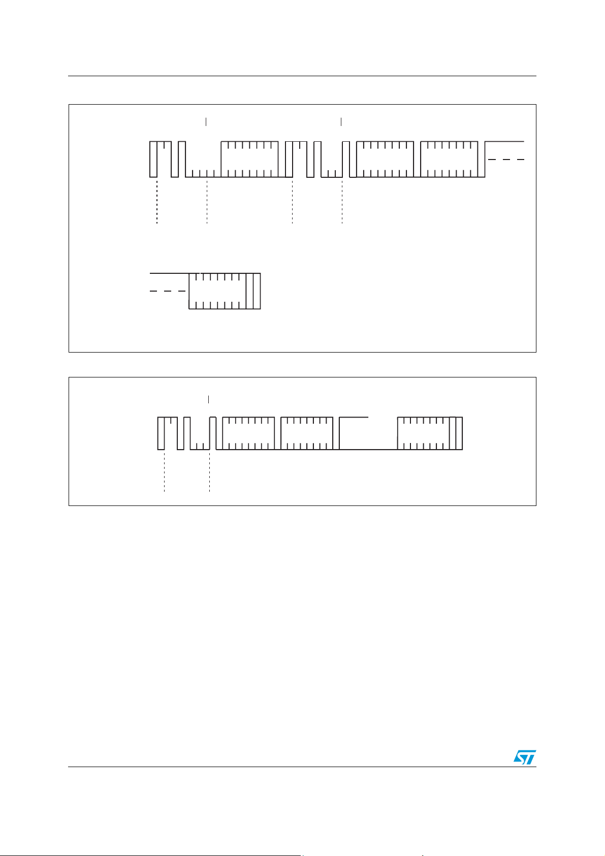
When TI/TP is a 1, the output is a free-running waveform as depicted in Figure 22. After
being low for the specified time (as shown in Ta bl e 1 1), the output automatically goes high
without need of software clearing any bits. The TF bit will still be set each time the timer
reloads, but it is not necessary for the software to clear it in this mode. Furthermore, clearing
the TF bit has no effect on the output in this mode.
While writes to the timer countdown register (10h) control the reload value, reads of this
register return the current countdown timer value.
Doc ID 12578 Rev 14 37/63
Page 38

Clock operation M41T82-M41T83
Table 10. Timer control register map
(1)
Addr D7 D6 D5 D4 D3 D2 D1 D0 Function
0Fh WDF AF1 AF2 BL TF OF 0 0 Flags
10h Timer countdown value
11h TE TI
1. Bit positions labeled with 0 should always be written with logic 0.
2. Writing to the timer register will not reset the TF bit nor clear the interrupt.
/TP TIE 0 0 0 TD1 TD0 Timer control
(2)
Timer value
When the timer is in the free-running mode, with a value of n programmed into the timer
countdown value, the output will nominally be low for one cycle of the specified clock source
and high for n-1 cycles with an overal period of n cycles. Thus, the countdown period is
n/source clock frequency.
For the special case of n = 1, as shown in Ta bl e 1 1, when the clock source is 4096 or 64 Hz,
the low time (T
) is half the clock period instead of a full clock period.
L
Table 11. Timer interrupt operation in free-running mode (with TI/TP = 1)
IRQ
low time – TL (seconds)
Source clock (Hz)
n = 1
(2)
4096 1/8192 = 122 µs 1/4096 = 244 µs 1/4096 = 244 µs n / 4096
64 1/128 = 7.8 ms 1/64 = 15.6 ms 1/64 = 15.6 ms n / 64
11/641/641 n
(1)
IRQ period – T
(seconds)
IRQ
n > 1 n = 1 n > 1
1/60 1/64 1/64 1 minute n minutes
1. IRQ1/FT/OUT is asserted coincident with TF going true.
2. n = loaded countdown timer value (0 < n < 255). The timer is stopped when n = 0.
Figure 22. Timer output waveform in free-running mode (with TI
T
IRQ
T
L
IRQ1/FT/OUT
/TP = 1)
AM03012v1
38/63 Doc ID 12578 Rev 14
Page 39

M41T82-M41T83 Clock operation
3.8.2 Timer flag (TF)
At the end of a timer countdown, when the timer reloads, TF is set to logic '1.' Regardless of
the state of TF bit (or TI
/TP bit), the timer will continue decrementing and reloading.
If both timer and alarm interrupts are used in the application, the source of the interrupt can
be determined by reading the flag bits. Refer to Section 3.14 for more information on the
interaction of these bits. The TF bit is cleared by reading the flags register. This will deassert an interrupt output due to the timer.
3.8.3 Timer interrupt enable (TIE, M41T83 only)
In normal interrupt mode (TI/TP = 0), when TF is asserted, the interrupt output is asserted (if
TIE = 1). To de-assert the interrupt, the TF bit or the TIE bit must be reset. Disabling the
interrupt by clearing the TIE bit will de-assert the output, but does not clear the TF bit. Thus,
if TIE is re-enabled prior to clearing TF, the interrupt will assert immediately.
3.8.4 Timer enable (TE)
● TE = 0
When the timer register (10h) is set to 0, the timer is disabled.
● TE = 1
The timer is enabled. TE is reset (disabled) on power-down. When re-enabled, the
counter will begin counting from the same value as when it was disabled.
3.8.5 TD1/0
These are the timer source clock frequency selection bits (see Ta bl e 1 2 ). These bits
determine the source clock for the countdown timer (see Table 10 on page 38). When not in
use, the TD1 and TD0 bits should be set to 11 (1/60 Hz) for power saving.
Table 12. Timer source clock frequency selection (244.1 µs to 4.25 hrs)
TD1 TD0 Timer source clock frequency (Hz)
0 0 4096 (244.1 µs)
0 1 64 (15.6 ms)
10 1 (1 s)
1 1 1/60 (60 s)
3.9 Square wave output (M41T83 only)
The M41T83 offers the user a programmable square wave function which is output on the
SQW pin. RS3-RS0 bits located in 13h establish the square wave output frequency. These
frequencies are listed in Ta bl e 1 3 . Once the selection of the SQW frequency has been
completed, the SQW pin can be turned on and off under software control with the square
wave enable bit (SQWE) located in register 0Ah.
Note: If the SQWE bit is set to '1' and V
wave output will be disabled.
falls below the switchover (VSO) voltage, the square
CC
Doc ID 12578 Rev 14 39/63
Page 40

Clock operation M41T82-M41T83
Table 13. Square wave output frequency
Square wave bits Square wave
RS3 RS2 RS1 RS0 Frequency Units
0000None–
000132.768kHz
00108.192kHz
00114.096kHz
01002.048kHz
01011.024kHz
0110512Hz
0111256Hz
1000128Hz
100164Hz
101032Hz
101116Hz
11008Hz
11014Hz
11102Hz
11111Hz
40/63 Doc ID 12578 Rev 14
Page 41

M41T82-M41T83 Clock operation
3.10 Battery low warning
The M41T8x automatically checks the battery each time VCC powers up and each time the
clock rolls over at midnight.
V
is compared to VBL (approximately 2.5 V), then the battery low (BL) bit, D4 of flags
BAT
register 0Fh, is set if the battery voltage is found to be less than V
greater than V
, the BL bit is cleared during battery check.
BL
The BL bit retains its state until the next battery check occurs. This means the BL bit will not
clear immediately upon battery replacement, but only after the next battery check occurs at
the next power-up or midnight rollover.
If a battery low is generated during a power-up sequence, this indicates that the battery is
below approximately 2.5 volts and may not be able to maintain data integrity. Clock data
should be considered suspect and verified as correct. A fresh battery should be installed.
If a battery low indication is generated during the 24-hour interval check, this indicates that
the battery is near end of life. However, data is not compromised due to the fact that a
nominal V
is supplied. In order to ensure data integrity during subsequent periods of
CC
battery backup mode, the battery should be replaced.
Midnight rollover check
As shown in Figure 23, during the midnight rollover check, the M41T8x applies a load to the
battery, then compares V
present, an open condition on the V
is performed, the RTC removes the load.
BAT
to V
and updates the BL bit accordingly. Because a load is
BL
pin will result in the BL bit being set. After the check
BAT
. Similarly, if V
BL
BAT
is
Power-up battery check
During the power-up check, no load is applied to the battery under the assumption the
battery has already been stressed to its working level by having powered the RTC in backup
mode. If no battery is present, V
indeterminate.
Figure 23. Battery check
V
BAT
Only at
rollover
R
L
will be floating and the battery check result will be
BAT
At power-up
and at rollover
VBL=2.5V
S
Q
FF
R
BL
AM03009v1
Doc ID 12578 Rev 14 41/63
Page 42

Clock operation M41T82-M41T83
The M41T8x only checks the battery when powered by VCC. It does not check the battery
while in backup mode. Thus, users are advised that during long periods in backup mode,
the battery can drop to a level at which timekeeping may fail or data becomes corrupted. If,
at power-up, a battery low is indicated, data integrity should be verified.
Forcing a battery check
If it is desired to check the battery at an arbitrary time, one common technique is for the
application software to write the time to just before midnight, 23:59:59, and then wait two
seconds thereby letting the clock rollover and causing the BL bit to update. The application
then restores the time back to its previous value plus two seconds.
3.11 Century bits
These two bits will increment in a binary fashion at the turn of the century, and handle all
leap years correctly. See Ta bl e 1 4 for additional explanation.
Table 14. Century bits examples
CB0 CB1 Leap Year? Example
00Yes2000
0 1 No 2100
(1)
1 0 No 2200
1 1 No 2300
1. Leap year occurs every four years (for years evenly divisible by four), except for years evenly divisible by
100. The only exceptions are those years evenly divisible by 400 (the year 2000 was a leap year, year
2100 is not).
3.12 Oscillator fail detection
If the oscillator fail (OF) bit is internally set to a '1,' this indicates that the oscillator has either
stopped, or was stopped for some period of time. This bit can be used to judge the validity of
the clock and date data. This bit will be set to '1' any time the oscillator stops.
In the event the OF bit is found to be set to '1' at any time other than the initial power-up, the
STOP bit (ST) should be written to a '1,' then immediately reset to 0. This will restart the
oscillator. The following conditions can cause the OF bit to be set:
● The first time power is applied (defaults to a '1' on power-up).
Note: If the OF bit cannot be written to '0' four seconds after the initial power-up, the STOP bit (ST)
should be written to a '1,' then immediately reset to 0.
● The voltage present on V
● The ST bit is set to '1.'
● External interference of the crystal
For the M41T83, if the oscillator fail interrupt enable bit (OFIE) is set to a '1,' the
IRQ1
/FT/OUT pin will also be asserted (see Section 3.13 and Section 3.14 for additional
conditions which apply). The IRQ1
0, NOT by reading the flags register. The OF bit will remain a '1' until written to 0. Reading
the flags register has no effect on OF.
or battery is insufficient to support oscillation.
CC
/FT/OUT output is de-asserted by resetting the OF bit to
42/63 Doc ID 12578 Rev 14
Page 43

M41T82-M41T83 Clock operation
The oscillator must start and have run for at least 4 seconds before attempting to reset the
OF bit to 0.
The oscillator fail detect circuit funtions during backup mode. If a triggering event occurs to
disrupt the oscillator during a power-down condition, the OF bit will be set accordingly.
3.13 Oscillator fail interrupt enable (M41T83 only)
With the OFIE bit set, the OF bit will cause the IRQ1/FT/OUT output to be asserted (see
Section 3.14.1 and 3.14.2 for additional conditions that apply). The IRQ1
/FT/OUT output is
cleared by resetting the OF bit to 0 (NOT by reading the flags register). Clearing the OFIE bit
will also cause the IRQ1
clearing OF, the IRQ1
/FT/OUT output to de-assert, but if OFIE is subsequently set prior to
/FT/OUT output will assert immediately upon setting OFIE. Clearing
the OF bit is necessary to prevent such an inadvertent interrupt.
If the alarm in backup enable bit, ABE, is set (along with OFIE), the oscillator fail detect will
cause an interrupt in the IRQ1
/FT/OUT pin during backup mode. For additional information
on this, refer to Section 3.14.2.
3.14 IRQ1/FT/OUT pin, frequency test, interrupts and the OUT bit (M41T83 only)
Four interrupt sources, the frequency test function, and the discrete output bit OUT all share
the IRQ1
others. Additionally, the priority depends on configuration bits such as OUT and ABE, and
on whether the part is operating on V
output and requires an external pull-up resistor.
Figure 24 shows the various signal sources and controlling bits for the IRQ1
pin.
Figure 24. IRQ1
TIMER
TE
Write OF to 0
to clear
Read FLAGS register
to clear
/FT/OUT pin. Priority is built into the part such that some functions dominate
or is in the backup mode. This pin is an open drain
CC
/FT/OUT output
/FT/OUT output pin circuit
OF
AF1
TI/TP
TIE
OFIE
AI1E
OUT
FT
ABE
A1IE
OFIE
TIE
w-dog running
IRQ1/OUT/FT
LOGIC
reload
TF
IRQ1/OUT/FT
Write watchdog register
to clear
WDF
PRE
WDOG
Q
Doc ID 12578 Rev 14 43/63
AM03013v1
Page 44

Clock operation M41T82-M41T83
The timer, oscillator fail detect circuit, alarm 1, and watchdog are ORed together as the
primary interrupt sources. The frequency test signal, FT, is used to enable a 512 Hz output
on the IRQ1
/FT/OUT pin for calibrating the RTC. When not used as an interrupt or
frequency test output, the pin can be used as a discrete logic output controlled by the OUT
bit. The ABE bit is used to enable interrupts during backup mode.
Operating on V
, all four interrupt sources are available. During backup, the timer and
CC
watchdog are disabled, and the only interrupt sources are alarm 1 and the oscillator fail
detect circuit.
3.14.1 Active mode operation on V
On VCC, the operation of the output circuit is as shown in Ta bl e 1 5.
Table 15. Priority for IRQ1
(1)
OUT
00 x 0
01 x
x1 0
1x 1 IRQ
10 0 1
FT
(2)
/FT/OUT pin when operating on V
(3)
A1IE
(4)
+ OFIE
(5)
+ TIE
+ watchdog
running
(6)
Pin Comment
512 Hz
CC
CC
When OUT is 0 and FT is not enabled, OUT dominates
and none of the interrupt sources have any effect.
When FT = 1 and OUT = 1 and no interrupts are enabled,
the output will be the 512 Hz frequency test (FT) signal.
When one or more interrupts are enabled, and OUT is a 1,
the pin stays high until one of the interrupts is asserted.
When OUT is 1, FT is 0 and no interrupts are enabled, the
pin is high.
1. OUT is bit 7 of register 08h (digital calibration).
2. FT is bit 6 of register 08h (digital calibration).
3. A1IE is bit 7 of register 0Ah (alarm 1, month).
4. OFIE is bit 7 of register 09h (watchdog).
5. TIE is bit 5 of register 11h (timer control).
6. The watchdog is controlled by register 09h (watchdog).
When OUT is 0 and FT is 0, the pin will be 0 regardless of whether any interrupts are
enabled.
When FT is a 1, the 512 Hz signal will be output if OUT is 0 or if no interrupts are enabled.
The interrupt sources control the pin when OUT is 1 and one or more of the interrupts are
enabled.
If OUT is 1, FT is 0 and no interrupts are enabled, then the pin will be 1.
44/63 Doc ID 12578 Rev 14
Page 45

M41T82-M41T83 Clock operation
3.14.2 Backup mode
In backup mode, the operation of the output circuit is as shown in Ta bl e 1 6 .
Table 16. Priority for IRQ1
(1)
OUT
x0 x 1
1x 0 1
01 x 0
11 1IRQ
1. OUT is bit 7 of register 08h (digital calibration).
2. ABE is bit 5 of register 0Ah (alarm 1, month).
3. A1IE is bit 7 of register 0Ah (alarm 1, month).
4. OFIE is bit 7 of register 09h (watchdog).
ABE
(2)
/FT/OUT pin when operating in backup mode
(3)
A1IE
+ OFIE
(4)
Pin Comment
In backup mode, frequency test is disabled. Thus, the FT bit is a ‘don’t care’.
ABE enables interrupts in backup. If it is 0, the output pin is a 1 regardless of the other bits.
The pin is also a 1 when OUT is a 1 and no interrupts are enabled.
When ABE is 0, the pin is 1 regardless of OUT or
the interrupt sources.
When OUT is 1 and no interrupts are enabled,
the pin is 1. (A1IE and OFIE are the only
interrupts applicable in this mode).
When ABE is 1 and OUT is 0, OUT dominates
and regardless of the interrupt sources.
When one or more interrupts are enabled, ABE is
a 1, and OUT is a 1, the pin stays high until one of
the interrupts is asserted.
When OUT is 0 and ABE is a 1, the pin is 0 regardless of the interrupts.
Thus, in order to enable interrupts in backup mode, OUT must be a 1 and ABE must be a 1,
and one or more of the interrupt enables must be a 1.
Simultaneous interrupts
Since more than one interrupt source can cause the IRQ1/FT/OUT pin to go low, more than
one interrupt may be pending when the microprocessor services the interrupt. Therefore,
the application software should read the flags register (0Fh) to discern which condition or
conditions are causing the pin to be asserted.
Also be aware that once a flag causes the pin to assert, other flags could subsequently also
go true. Since the pin is already low due to the first, no additional output transition will occur.
That is why the software must check the flags register.
Example: If the watchdog is in use and the oscillator fail detect interrupt is enabled, and the
watchdog times out, the IRQ1
processor services the interrupt, something disturbs the oscillator, such as a drop of
moisture landing on the crystal pins, the OF bit will also be set. Thus, when the software
services the interrupt, it must service both sources: it must re-initialize the watchdog and
clear the OF bit in order to de-assert the IRQ1
software will know both flags were set and that both need service.
/FT/OUT pin will go low. If, in the intervening time before the
/FT/OUT pin. By reading the flags register, the
Doc ID 12578 Rev 14 45/63
Page 46

Clock operation M41T82-M41T83
3.15 FT/RST pin, frequency test and reset output pin (M41T82 only)
On the M41T82, the 512 Hz frequency test signal and the reset output share the same pin,
FT/RST
the pin. With FT a 0 and V
enabled when V
. When the FT bit (bit 6 of register 08h) is a 1, the 512 Hz test signal is activated on
good (above V
fails, the FT bit will be cleared and the output will go low to assert reset.
CC
CC
), the output will be high. If the 512 Hz is
RST
At power-up, FT will be 0 leaving the pin functioning as the reset output.
3.16 Initial power-on defaults
Upon initial application of power to the device, the register bits will initially power-on in the
state indicated in Ta bl e 1 7 and Tab le 1 8 .
Table 17. Initial power-on default values (part 1)
DCS
Condition
Initial
power-up
Subsequent
power-up
1. All other control bits power-up in an undetermined state.
2. M41T83 only
3. BMB0-BMB4, RB0, RB1
4. With battery backup
5. UC = unchanged
Table 18. Initial power-up default values (part 2)
Condition
Initial
power-up
Subsequent
power-up
1. All other control bits power-up in an undetermined state.
2. M41T83 only
3. With battery backup
4. UC = unchanged
(1)
ST CB1 CB0 OUT FT
00 0 100 0 0 0 0 0 1 0
UC UC UC UC 0 UC UC UC UC 0 UC UC UC
(4)(5)
(1)
RPT11
-15
HT OF TE
TI/TP
(2)
01100 01110 0 0 0 0
(3)(4)
UC 1 UC 0 UC UC UC UC UC UC UC UC UC UC
ACS
TIE
Digital
calib.
(2)
TD1 TD0 RS0 RS1-3
Analog
calib.
OFIE
(2)
Watch-
(3)
dog
OTP
(2)
A1IE
A2IE
(2)
(2)
SQWE
RPT21-
25
(2)
ABE
AL2E
46/63 Doc ID 12578 Rev 14
Page 47

M41T82-M41T83 Clock operation
3.17 OTP bit operation (M41T83 in SOX18 package only)
When the OTP (one time programmable) bit is set to a '1,' the value in the internal OTP
registers will be transferred to the analog calibration register (12h) and are “Read only.” The
OTP value is programmed by the manufacturer, and will contain the calibration value
necessary to achieve ±5 ppm (V
clock accuracy can then be guaranteed to drift no more than ±3 ppm the first year, and
±1 ppm for each following year due to crystal aging.
If the OTP bit is set to 0, the analog calibration register will become a WRITE/READ register
and function like standard SRAM memory cells, allowing the user to implement any desired
value of analog calibration.
When the user sets the OTP bit, they need to wait for approximately 8 ms before the analog
registers transfer the value from the OTP to the analog registers due to the OTP read
operation.
only) at room temperature after two SMT reflows. This
CC
Doc ID 12578 Rev 14 47/63
Page 48

Maximum ratings M41T82-M41T83
4 Maximum ratings
Stressing the device above the rating listed in the absolute maximum ratings table may
cause permanent damage to the device. These are stress ratings only and operation of the
device at these or any other conditions above those indicated in the operating sections of
this specification is not implied. Exposure to absolute maximum rating conditions for
extended periods may affect device reliability.
Table 19. Absolute maximum ratings
Sym Parameter Value
(1)
Unit
T
T
STG
V
SLD
V
I
P
Storage temperature (VCC off, oscillator off) –55 to 125 °C
Supply voltage –0.3 to 7.0 V
CC
QFN16
260
Lead solder temperature for 10 seconds
SOX18 240
Input or output voltages –0.2 to VCC+0.3 V
IO
Output current 20 mA
O
Power dissipation 1 W
D
(2)
(3)
QFN16 35.7
θ
Thermal resistance, junction to ambient
JA
SOX18
1. Data based on characterization results, not tested in production.
2. Reflow at peak temperature of 260 °C. The time above 255 °C must not exceed 30 seconds.
3. Reflow at peak temperature of 240 °C. The time above 235 °C must not exceed 20 seconds.
°CSO8
°C/WSO8 128.4
48/63 Doc ID 12578 Rev 14
Page 49

M41T82-M41T83 DC and AC parameters
5 DC and AC parameters
This section summarizes the operating and measurement conditions, as well as the dc and
ac characteristics of the device. The parameters in the following DC and AC Characteristic
tables are derived from tests performed under the measurement conditions listed in the
relevant tables. Designers should check that the operating conditions in their projects match
the measurement conditions when using the quoted parameters.
Table 20. Operating and AC measurement conditions
Parameter
(1)
M41T8x
Supply voltage (V
Ambient operating temperature (T
Load capacitance (C
) 2.38 V to 5.5 V
CC
) –40 to 85 °C
A
) 50 pF
L
Input rise and fall times ≤ 5 ns
Input pulse voltages 0.2 VCC to 0.8 V
Input and output timing ref. voltages 0.3 VCC to 0.7 V
1. Output Hi-Z is defined as the point where data is no longer driven.
Figure 25. Measurement AC I/O waveform
0.8V
CC
0.2V
CC
Table 21. Capacitance
Symbol Parameter
C
IN
C
OUT
t
LP
1. Effective capacitance measured with power supply at 3.6 V; sampled only, not 100% tested.
2. At 25 °C, f = 1 MHz
3. Outputs deselected
Input capacitance 7 pF
(3)
Output capacitance 10 pF
Low-pass filter input time constant (SDA and SCL) 50 ns
(1)(2)
0.7V
CC
0.3V
CC
Min Max Unit
CC
CC
AI02568
Doc ID 12578 Rev 14 49/63
Page 50

DC and AC parameters M41T82-M41T83
Table 22. DC characteristics
Sym Parameter Test condition
Operating voltage (S) –40 to 85 °C 3.00 5.50 V
V
Operating voltage (R) –40 to 85 °C 2.70 5.50 V
CC
Operating voltage (Z) –40 to 85 °C 2.38 5.50 V
(1)
Min Typ Max Unit
Input leakage current 0V ≤ V
I
LI
Output leakage current 0V ≤ V
I
LO
IN
OUT
≤ V
≤ V
CC
CC
5.5 V 125 150 µA
I
CC1
Supply current
SCL = 400 kHz
(No load)
3.0 V 55 µA
2.5 (Z only) 45 µA
I
Supply current (standby)
CC2
SCL = 0 Hz;
All inputs ≥ VCC – 0.2 V or
≤ VSS + 0.2 V
5.5 V 8 10 µA
3.0 V 6.5 µA
(SQWE bit = 0)
Input low voltage –0.3 0.3V
V
IL
V
Input high voltage 0.7V
IH
VCC/V
VOLOutput low voltage
RS
SQW, IRQ1
T, FT/RST
/FT/OUT, IRQ2
SCL, SDA
V
Output high voltage VCC = 3.0 V, IOH = –1.0 mA (push-pull) 2.4 V
OH
Pull-up supply voltage
(open drain)
Backup supply voltage
V
BAT
(battery or capacitor)
Battery low (BL bit)
V
BL
threshold
/FT/OUT, IRQ2, FT/RST, RST 5.5 V
IRQ1
= 3.0 V,
BAT
= 1.0 mA
I
OL
VCC = 3.0 V,
= 1.0 mA
I
OL
V
= 3.0 V,
CC
= 3.0 mA
I
OL
CC
2.0 5.5 V
2.5 V
±1 µA
±1 µA
CC
VCC+0.3 V
0.4 V
0.4 V
0.4 V
V
I
Battery supply current
BAT
1. Valid for ambient operating temperature: TA = –40 to 85 °C; VCC = 2.38 V to 5.5 V (except where noted)
25 °C; VCC = 0 V; OSC on;
= 3 V; SQW off
V
BAT
365 450 nA
50/63 Doc ID 12578 Rev 14
Page 51

M41T82-M41T83 DC and AC parameters
Figure 26. I
Table 23. Crystal electrical characteristics
Symbol Parameter
f
O
R
S
C
L
1. Externally supplied if using the QFN16 or SO8 package. STMicroelectronics recommends the Citizen CFS-
145 (1.5 x 5 mm) and the KDS DT-38 (3 x 8 mm) for thru-hole, or the KDS DMX-26S (3.2 x 8 mm) or Micro
Crystal MS3V-T1R (1.5 x 5 mm) for surface-mount, tuning fork-type quartz crystals. For contact
information, see Section 8: References on page 61.
2. Load capacitors are integrated within the M41T8x. Circuit board layout considerations for the 32.768 kHz
crystal of minimum trace lengths and isolation from RF generating signals should be taken into account.
vs. temperature
CC2
10.000
9.000
8.000
7.000
6.000
Icc2 (µA)
5.000
4.000
3.000
2.000
-40 -20 0 20 40 60 80
Temperature (°C)
(1)(2)
Min Typ Max Units
(3.0V)
(5.0V)
ai 13909
Resonant frequency 32.768 kHz
Series resistance 65
(3)
kΩ
Load capacitance 12.5 pF
3. Guaranteed by design.
Table 24. Oscillator characteristics
Symbol Parameter
V
C
XI, CXO
t
STA
STA
Oscillator start voltage ≤ 4 s 2.0 V
Oscillator start time VCC = V
(1)
Capacitor input, capacitor output 25 pF
(1)(2)
IC-to-IC frequency variation
1. With default analog calibration value ( = 0)
2. Reference value
3. TA = 25 °C, VCC = 5.0 V
Doc ID 12578 Rev 14 51/63
(2)(3)
Conditions Min Typ Max Units
SO
1s
–10 +10 ppm
Page 52

DC and AC parameters M41T82-M41T83
Figure 27. Power down/up mode AC waveforms
V
CC
V
V
RST
SO
t
rec
SDA, SCL
t
RD
RST
Table 25. Power down/up trip points DC characteristics
Sym Parameter
V
Reset threshold voltage
RST
(1)(2)
DON'T CARE
AI00596
Min Typ Max Unit
S 2.85 2.93 3.0 V
R 2.55 2.63 2.7 V
Z 2.252.322.38 V
V
Battery backup switchover V
SO
Hysteresis 25 mV
t
t
1. All voltages referenced to V
RST duration after VCC high 140 280 ms
rec
VCC to reset delay
RD
SS
(3)
RST
2.5 µs
2. Valid for ambient operating temperature: TA = –40 to 85 °C; VCC = 2.38 to 5.5 V (except where noted)
3. Measured with VCC falling slew rate of 10 mV/µs for VCC in the range V
+ 100 mV to V
RST
– 100 mV
RST
V
52/63 Doc ID 12578 Rev 14
Page 53

M41T82-M41T83 DC and AC parameters
Figure 28. Bus timing requirement sequence
SDA
t
BUF
SCL
SP
Table 26. AC characteristics
t
HD:STA
t
R
Sym Parameter
f
SCL
t
LOW
t
HIGH
t
HD:STA
t
SU:STA
t
SU:DAT
t
HD:DAT
t
SU:STO
t
BUF
SCL clock frequency 0 400 kHz
Clock low period 1.3 µs
Clock high period 600 ns
SDA and SCL rise time 300 ns
t
R
SDA and SCL fall time 300 ns
t
F
START condition hold time
(after this period the first clock pulse is generated)
START condition setup time
(only relevant for a repeated start condition)
(2)
Data setup time 100 ns
Data hold time 0 µs
STOP condition setup time 600 ns
Time the bus must be free before a new transmission
can start
t
t
LOW
t
F
HIGH
(1)
t
t
HD:DAT
SU:DAT
t
HD:STA
SR
t
SU:STA
t
SU:STO
P
AI00589
Min Typ Max Units
600 ns
600 ns
1.3 µs
1. Valid for ambient operating temperature: TA = –40 to 85 °C; VCC = 2.38 to 5.5 V (except where noted).
2. Transmitter must internally provide a hold time to bridge the undefined region (300 ns max) of the falling
edge of SCL.
Doc ID 12578 Rev 14 53/63
Page 54

Package mechanical data M41T82-M41T83
6 Package mechanical data
In order to meet environmental requirements, ST offers these devices in different grades of
ECOPACK
specifications, grade definitions and product status are available at: www.st.com.
ECOPACK
®
packages, depending on their level of environmental compliance. ECOPACK®
®
is an ST trademark.
54/63 Doc ID 12578 Rev 14
Page 55

M41T82-M41T83 Package mechanical data
Figure 29. QFN16 – 16-lead, quad, flat package, no lead, 4 x 4 mm body size outline
D
E
Note: Drawing is not to scale.
Table 27. QFN16 – 16-lead, quad, flat package, no lead, 4 x 4 mm pack. mech. data
Sym
Typ Min Max Typ Min Max
A 0.90 0.80 1.00 0.035 0.031 0.039
A1 0.02 0.00 0.05 0.001 0.000 0.002
A3 0.20 – – 0.008 – –
ddd
E2
A3
C
b
L
D2
e
1
2
3
A1
A
mm inches
QFN16-A
b 0.30 0.25 0.35 0.012 0.010 0.014
D 4.00 3.90 4.10 0.157 0.154 0.161
D2 – 2.50 2.80 – 0.098 0.110
E 4.00 3.90 4.10 0.157 0.154 0.161
E2 – 2.50 2.80 – 0.098 0.110
e0.65– –0.026– –
L 0.40 0.30 0.50 0.016 0.012 0.020
ddd – 0.08 – – 0.003 –
Doc ID 12578 Rev 14 55/63
Page 56

Package mechanical data M41T82-M41T83
Figure 30. QFN16 – 16-lead, quad, flat package, no lead, 4 x 4 mm, recommended
footprint
2.70
0.70
0.20
4.50
Note: Dimensions are shown in millimeters (mm).
Figure 31. 32 KHz crystal + QFN16 vs. VSOJ20 mechanical data
6.0 ± 0.2
3.2
SMT
1
2
3
4
CRYSTAL
161514
XI
XO
ST QFN16
1.5
3.9
2.70
0.35
0.325
0.65
VSOJ20
13
7.0 ± 0.3
AI11815
3.9
Note: Dimensions shown are in millimeters (mm).
56/63 Doc ID 12578 Rev 14
AI11816
Page 57

M41T82-M41T83 Package mechanical data
Figure 32. SOX18 – 18-lead plastic small outline, 300 mils, embedded crystal, outline
Note: Drawing is not to scale.
Table 28. SOX18 – 18-lead plastic small outline, 300 mils, embedded crystal,
package mech. data
Symbol
Typ Min Max Typ Min Max
A 2.57 2.44 2.69 0.101 0.096 0.106
A1 0.23 0.15 0.31 0.009 0.006 0.012
A2 2.34 2.29 2.39 0.092 0.090 0.094
B 0.46 0.41 0.51 0.018 0.016 0.020
c 0.25 0.20 0.31 0.010 0.008 0.012
D 11.61 11.56 11.66 0.457 0.455 0.459
E 7.62 7.57 7.67 0.300 0.298 0.302
E1 10.34 10.16 10.52 0.407 0.400 0.414
e 1.27 – – 0.050 – –
L 0.66 0.51 0.81 0.026 0.020 0.032
SOX1 8
millimeters inches
Doc ID 12578 Rev 14 57/63
Page 58

Package mechanical data M41T82-M41T83
Figure 33. SO8 – 8-lead plastic small package outline
h x 45°
A2
b
e
D
8
1
Note: Drawing is not to scale.
Table 29. SO8 – 8-lead plastic small outline (150 mils body width), package mech.
data
Symb
Typ Min Max Typ Min Max
A 1.75 0.069
A1 0.10 0.25 0.004 0.010
A2 1.25 0.049
A
ccc
0.25 mm
GAUGE PLANE
E1
E
A1
L
L1
mm inches
c
k
SO-A
b 0.28 0.48 0.011 0.019
c 0.17 0.23 0.007 0.009
ccc 0.10 0.004
D 4.90 4.80 5.00 0.193 0.189 0.197
E 6.00 5.80 6.20 0.236 0.228 0.244
E1 3.90 3.80 4.00 0.154 0.150 0.157
e 1.27 - - 0.050 - -
h 0.25 0.50 0.010 0.020
k 0°8° 0°8°
L 0.40 0.127 0.016 0.050
L1 1.04 0.041
58/63 Doc ID 12578 Rev 14
Page 59

M41T82-M41T83 Package mechanical data
Figure 34. Carrier tape for QFN16, SOX18, and SO8 packages
P
D
T
A
TOP COVER
TAPE
K
0
0
CENTER LINES
OF CAVITY
P
2
B
0
0
P
1
E
F
W
USER DIRECTION OF FEED
Table 30. Carrier tape dimensions for QFN16, SOX18, and SO8 packages
Package W D E P
1.50
+0.10/
–0.00
1.50
+0.10/
–0.00
1.50
+0.10/
–0.00
1.75
±0.10
1.75
±0.10
1.75
±0.10
4.00
±0.10
4.00
±0.10
4.00
±0.10
QFN16
SOX18
SO8
12.00
±0.30
24.00
±0.30
12.00
±0.30
P
0
2.00
±0.10
2.00
±0.10
2.00
±0.10
FA0B
2
5.50
±0.05
11.50
±0.10
5.50
±0.05
4.30
±0.10
12.70
±0.10
6.50
±0.10
0
4.30
±0.10
11.90
±0.10
5.30
±0.10
K
0
1.10
±0.10
3.20
±0.10
2.20
±0.10
P
1
8.00
±0.10
16.00
±0.10
8.00
±0.10
AM03073v1
TUnit
0.30
0.30
0.30
mm 1000
mm 1000
mm 2500
±0.05
±0.05
±0.05
Bulk
Qty
Doc ID 12578 Rev 14 59/63
Page 60

Part numbering M41T82-M41T83
7 Part numbering
Table 31. Ordering information
Example: M41T 83 S QA 6 F
Device family
M41T
Device type
82 (SO8 package only)
83
Operating voltage
S = V
R = V
Z = V
= 3.00 to 5.5 V
CC
= 2.70 to 5.5 V
CC
= 2.38 to 5.5 V
CC
Package
QA = QFN16 (4 mm x 4 mm)
(1)
M
= SO8
(2)
MY
= SOX18
Temperature range
6 = –40 °C to 85 °C
Shipping method
®
F = ECOPACK
1. M41T82 only
2. The SOX18 package includes an embedded 32,768 Hz crystal.
package, tape & reel
For other options, or for more information on any aspect of this device, please contact the
ST sales office nearest you.
60/63 Doc ID 12578 Rev 14
Page 61

M41T82-M41T83 References
8 References
Below is a listing of the crystal component suppliers mentioned in this document.
● KDS can be contacted at kouhou@kdsj.co.jp or http://www.kdsj.co.jp.
● Citizen can be contacted at csd@citizen-america.com or
http://www.citizencrystal.com.
● Micro Crystal can be contacted at sales@microcrystal.ch or
http://www.microcrystal.com.
Doc ID 12578 Rev 14 61/63
Page 62

Revision history M41T82-M41T83
9 Revision history
Table 32. Document revision history
Date Revision Changes
Updated Ta bl e 1 , 2, 4, 6, 10, 11, 22, Figure 20, 27, Section 3, Section 3.4.1,
Section 3.4.2, Section 3.5, Section 3.6, Section 3.7, Section 3.8,
Section 3.8.2, Section 3.8.3, Section 3.8.4, Section 3.8.5, Section 3.12,
09-Apr-2009 9
Section 3.13, Section 6; added Section 3.8.1, Section 3.14, Section 3.15,
Ta bl e 9 , 15, 16, Figure 22, 24; removed “output driver pin” section, “alarm
interrupt reset waveform” figure, “backup mode alarm waveform” figure, “timer
countdown value register bits (addr 11h)” table; added tape and reel
information Figure 34, Ta bl e 3 0 .
05-Jan-2010 10
25-Mar-2010 11 Updated Figure 27; Ta b le 2 5 .
19-Oct-2010 12 Updated Note in Section 3.12: Oscillator fail detection.
12-Oct-2011 13
16-May-2012 14
Updated Section 2.2: Read mode, Section 2.3: Write mode, Section 3: Clock
operation, Section 3.1, Section 3.2, Ta bl e 2 6 .
Updated Features, title,
bit (HT) operation; added Figure 16, added footnote 3 to Table 31: Ordering
information.
Added reference to AN1572 in Section 3.2.1: Power-down time-stamp; textual
update to Section 3.17: OTP bit operation (M41T83 in SOX18 package only);
updated test condition for I
shipping method in tubes from Table 31: Ordering information.
Section 3.1: Clock data coherency, Section 3.2: Halt
in Table 22: DC characteristics; removed
BAT
62/63 Doc ID 12578 Rev 14
Page 63

M41T82-M41T83
Please Read Carefully:
Information in this document is provided solely in connection with ST products. STMicroelectronics NV and its subsidiaries (“ST”) reserve the
right to make changes, corrections, modifications or improvements, to this document, and the products and services described herein at any
time, without notice.
All ST products are sold pursuant to ST’s terms and conditions of sale.
Purchasers are solely responsible for the choice, selection and use of the ST products and services described herein, and ST assumes no
liability whatsoever relating to the choice, selection or use of the ST products and services described herein.
No license, express or implied, by estoppel or otherwise, to any intellectual property rights is granted under this document. If any part of this
document refers to any third party products or services it shall not be deemed a license grant by ST for the use of such third party products
or services, or any intellectual property contained therein or considered as a warranty covering the use in any manner whatsoever of such
third party products or services or any intellectual property contained therein.
UNLESS OTHERWISE SET FORTH IN ST’S TERMS AND CONDITIONS OF SALE ST DISCLAIMS ANY EXPRESS OR IMPLIED
WARRANTY WITH RESPECT TO THE USE AND/OR SALE OF ST PRODUCTS INCLUDING WITHOUT LIMITATION IMPLIED
WARRANTIES OF MERCHANTABILITY, FITNESS FOR A PARTICULAR PURPOSE (AND THEIR EQUIVALENTS UNDER THE LAWS
OF ANY JURISDICTION), OR INFRINGEMENT OF ANY PATENT, COPYRIGHT OR OTHER INTELLECTUAL PROPERTY RIGHT.
UNLESS EXPRESSLY APPROVED IN WRITING BY TWO AUTHORIZED ST REPRESENTATIVES, ST PRODUCTS ARE NOT
RECOMMENDED, AUTHORIZED OR WARRANTED FOR USE IN MILITARY, AIR CRAFT, SPACE, LIFE SAVING, OR LIFE SUSTAINING
APPLICATIONS, NOR IN PRODUCTS OR SYSTEMS WHERE FAILURE OR MALFUNCTION MAY RESULT IN PERSONAL INJURY,
DEATH, OR SEVERE PROPERTY OR ENVIRONMENTAL DAMAGE. ST PRODUCTS WHICH ARE NOT SPECIFIED AS "AUTOMOTIVE
GRADE" MAY ONLY BE USED IN AUTOMOTIVE APPLICATIONS AT USER’S OWN RISK.
Resale of ST products with provisions different from the statements and/or technical features set forth in this document shall immediately void
any warranty granted by ST for the ST product or service described herein and shall not create or extend in any manner whatsoever, any
liability of ST.
ST and the ST logo are trademarks or registered trademarks of ST in various countries.
Information in this document supersedes and replaces all information previously supplied.
The ST logo is a registered trademark of STMicroelectronics. All other names are the property of their respective owners.
© 2012 STMicroelectronics - All rights reserved
STMicroelectronics group of companies
Australia - Belgium - Brazil - Canada - China - Czech Republic - Finland - France - Germany - Hong Kong - India - Israel - Italy - Japan -
Malaysia - Malta - Morocco - Philippines - Singapore - Spain - Sweden - Switzerland - United Kingdom - United States of America
www.st.com
Doc ID 12578 Rev 14 63/63
 Loading...