

Page 1
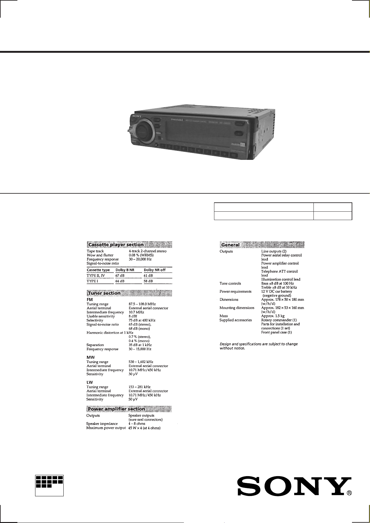
XR-C8220R
SERVICE MANUAL
For RM-X4S (Remote Commander),
please refer to RM-X4S Service Manual
(9-925-698-∏) previously issued.
Dolby noise reduction manufactured under license
from Dolby Laboratories Licensing Corporation.
“DOLBY” and the double-D symbol a are trademarks of Dolby Laboratories Licensing Corporation.
SPECIFICA TIONS
AEP Model
UK Model
Model Name Using Similar Mechanism XR-C8100R
T ape Transport Mechanism Type MG-25D-136
MICROFILM
FM/MW/LW CASSETTE CAR STEREO
Page 2
SECTION 1
SERVICE NOTE
TABLE OF CONTENTS
1. SERVICE NOTE....................................................... 2
2. GENERAL
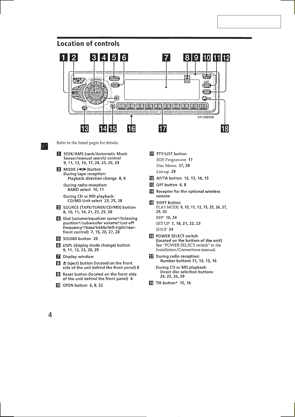
Location of Controls ....................................................... 3
Resetting the Unit ........................................................... 4
Setting the Clock ............................................................. 4
Other Functions............................................................... 4
Installation....................................................................... 6
Connections ..................................................................... 7
3. DISASSEMBLY ......................................................... 12
4. ASSEMBLY OF MECHANISM DECK........... 14
5. MECHANICAL ADJUSTMENTS....................... 17
6. ELECTRICAL ADJUSTMENTS
Test Mode........................................................................ 18
Tape Deck Section .......................................................... 18
Tuner Section .................................................................. 19
7. DIAGRAMS
7-1. Block Diagram – TUNER Section – .............................. 23
7-2. Block Diagram – TAPE Section – .................................. 25
7-3. Block Diagram – MAIN Section – ................................. 27
7-4. Block Diagram
– DISPLAY/KEY CONTROL Section –........................ 29
7-5. Block Diagram
– BUS CONTROL/POWER SUPPLY Section –........... 31
7-6. Note for Printed Wiring Boards and
Schematic Diagrams ....................................................... 33
7-7. Printed Wiring Board
– MAIN Board (Component Side) – .............................. 35
7-8. Printed Wiring Board
– MAIN Board (Conductor Side) – ................................ 37
7-9. Schematic Diagram – MAIN Board (1/4) – ................... 39
7-10. Schematic Diagram – MAIN Board (2/4) – ................... 41
7-11. Schematic Diagram – MAIN Board (3/4) – ................... 43
7-12. Schematic Diagram – MAIN Board (4/4) – ................... 45
7-13. Printed Wiring Board – KEY Board –............................ 47
7-14. Schematic Diagram – KEY Board – .............................. 49
7-15. Printed Wiring Boards – SUB/INVERTER Boards – .... 51
7-16. Schematic Diagram
– SUB/INVERTER Boards –.......................................... 52
7-17. IC Pin Function Description ........................................... 58
• Model Identification
The destination is expressed with the model according to the language of CSV (Computer Sound Voice) mounted in the set.
How to identify the model is described below.
– MAIN BOARD (Component Side) –
IC650
MSM6656A-687GS-KR1 (TYPE A: ENGLISH, FRENCH)
MSM6656A-688GS-KR1 (TYPE B: ENGLISH, GERMAN)
MSM6656A-689GS-KR1 (TYPE C: ENGLISH, SPANISH)
MSM6656A-690GS-KR1 (TYPE D: ENGLISH, ITALIAN)
8. EXPLODED VIEWS ................................................ 62
9. ELECTRICAL PARTS LIST ............................... 65
Flexible Circuit Board Repairing
• Keep the temperature of the soldering iron around 270 ˚C during repairing.
• Do not touch the soldering iron on the same conductor of the
circuit board (within 3 times).
• Be careful not to apply force on the conductor when soldering
or unsoldering.
Notes on chip component replacement
• Never reuse a disconnected chip component.
• Notice that the minus side of a tantalum capacitor may be damaged by heat.
– 2 –
Page 3
SECTION 2
GENERAL
This section is extracted from
instruction manual.
– 3 –
Page 4
– 4 –
Page 5
– 5 –
Page 6
– 6 –
Page 7
– 7 –
Page 8
– 8 –
Page 9
– 9 –
Page 10
– 10 –
Page 11
– 11 –
Page 12
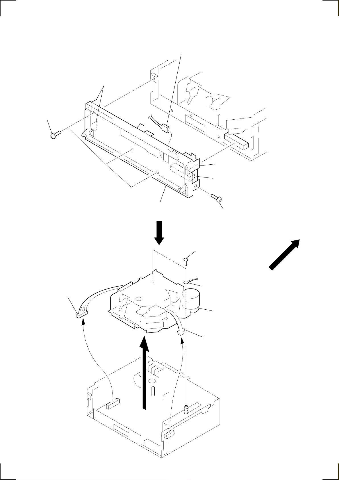
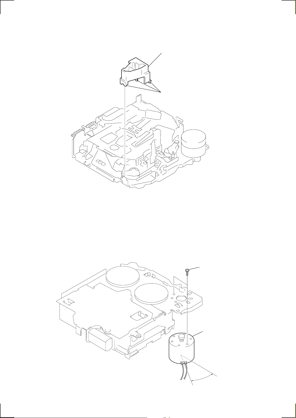
SECTION 3
DISASSEMBLY
Note: Follow the disassembly procedure in the numerical order given.
SUB PANEL ASS’Y
3
two claws
2
three screws
(PTT2.6 × 6)
1
connector
(CN802)
3
claw
4
connector
(CN500)
MECHANISM DECK (MG-25D-136)
1
connector
(CN201)
5
sub panel ass’y
3
two screws
(2.6 × 6)
4
2
lag
2
screw
(PTT2.6 × 6)
5
mechanism deck
(MG-25D-136)
flexible flat cable
(CN250)
– 12 –
Page 13
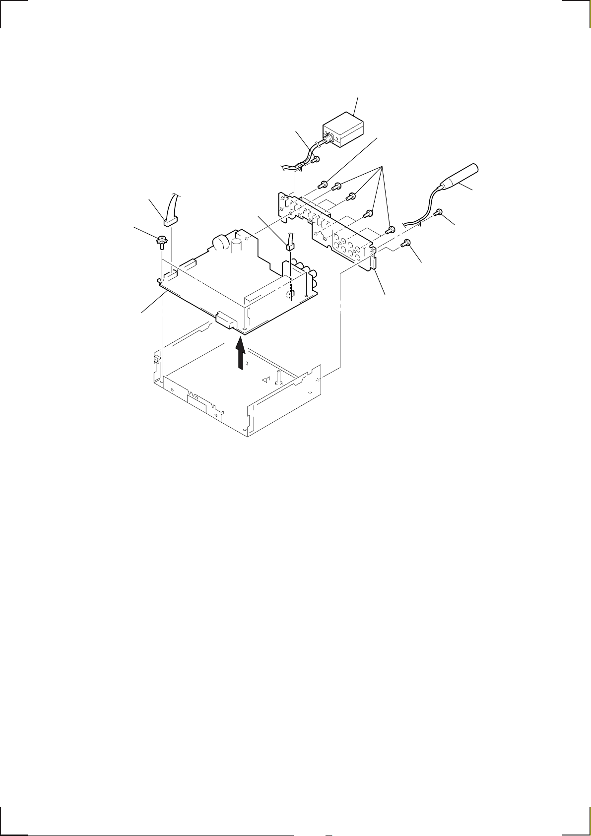
MAIN BOARD, HEAT SINK
4
main board
2
three ground point
screws
1
connector
(CN553)
1
connector
(J10)
5
screw
(PTT2.6 × 10)
3
screw
(PTT2.6 × 10)
7
screw
(PTT2.6 × 10)
9
seven screws
(PTT2.6 × 10)
8
cord (with connector)
(ANT)
6
inverter ass’y
3
screw
(PTT2.6 × 10)
0
heat sink
– 13 –
Page 14
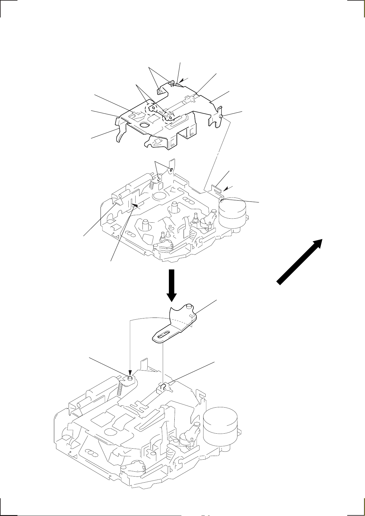
SECTION 4
ASSEMBLY OF MECHANISM DECK
Note: Follow the assembly procedure in the numerical order given.
HOUSING
4
Fit claw on B part.
3
Put the housing
under A part.
housing
2
Install the hanger onto
two claws of the housing.
5
Fit projection on C part.
C
part
7
Holder the hanger by bending the claw.
1
Install the catch to the hanger.
hanger
6
Fit projection on D part.
8
Hold the hanger by
bending the claw.
ARM (SUCTION)
A
part
projection
B
part
D
part
2
Move the arm (suction) in the arrow
direction and fit on projection.
1
Fit the arm (suction) on the shaft.
– 14 –
Page 15
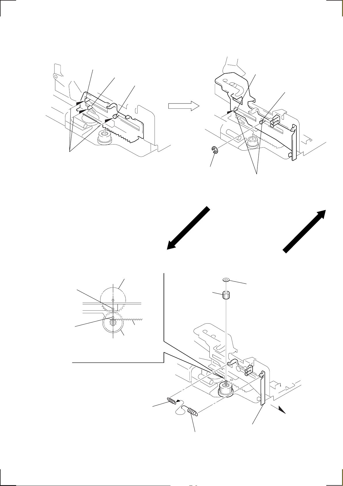
LEVER (LDG-A)/(LDG-B)
shaft
A
1
Fit the lever (LDG-A) on
shafts A – C and install it.
shaft
B
shaft
C
3
type-E stop ring 2.0
shaft
A
Fit the lever (LDG-B) on
2
shafts
install it.
A
and B and
shaft
B
GEAR (LDG-FT)
hole
hole
gear (LDG-D)
lever (LDG-A)
gear (LDG-FB)
4
Align hole in the gear (LDG-D)
with hole the lever (LDG-A).
2
tension spring (LD-2)
5
gear (LDG-FT)
1
6
polyethylene washer
2
tension spring (LD-1)
– 15 –
3
Move the lever (LDG-B)
in the arrow direction.
Page 16
GUIDE (C)
2
guide (C)
1
three claws
MOUNTING POSITION OF CAPSTAN/REEL MOTOR (M901)
two precision screws
×
2)
(P2
capstan/reel motor
(M901)
30˚
– 16 –
Page 17
SECTION 5
MECHANICAL ADJUSTMENTS
1. Clean the follo wing parts with a denatured-alcohol-moistened
swab:
playback head pinch roller
rubber belt capstan
idler
2. Demagnetize the playback head with a head demagnetizer.
3. Do not use a magnetized screwdriver for the adjustments.
4. After the adjustments, apply suitable locking compound to the
parts adjusted.
5. The adjustments should be performed with the power supply
voltage unless otherwise noted.
• T orque Measurement
Mode Torque Meter Meter Reading
Forward CQ-102C
Forward
Back Tension (0.01 – 0.06 oz•inch)
Reverse CQ-102RC
Reverse
Back Tension (0.01 – 0.06 oz•inch)
FF, REW CQ-201B
CQ-102C
CQ-102RC
30 – 65 g•cm
(0.42 – 0.90 oz•inch)
0.5 – 4.5g•cm
30 – 65 g•cm
(0.42 – 0.90 oz•inch)
0.5 – 4.5g•cm
60 – 200 g•cm
(0.83 – 2.78 oz•inch)
• T ape Tension Measurement
Mode Tension Meter Meter Reading
Forward CQ-403A
Reverse CQ-403R
(more than 3.18 oz)
(more than 3.18 oz)
more than 90 g
more than 90 g
– 17 –
Page 18
set
+
–
test tape
P-4-D400
(400Hz, 0 dB) level meter
MAIN board
TP (DOLBY-L)/
TP (DOLBY-R)
SECTION 6
ELECTRICAL ADJUSTMENTS
TEST MODE
This set have the test mode function. In the test mode, FM Auto
Scan/Stop Level and MW Auto Scan/Stop Level adjustments can
be performed easier than it in ordinary procedure.
<Set the Test Mode>
1. Set the “power select” switch (S600) is “A (ON)” position.
2. Turn ON the regulated power supply. (The clock is displayed)
Note: Press the [OFF] button, if the clock is not displayed.
3. Push the preset [4] button.
4. Push the preset [5] button.
5. Press the preset [1] button for more than two seconds.
6. Then the display indicates all lights, the test mode is set.
<Release the Test mode>
1. Push the [OFF] button.
2. Return the “power select” switch (S600) to initially set position.
See the adjustment location from on page 22 for the
adjustment.
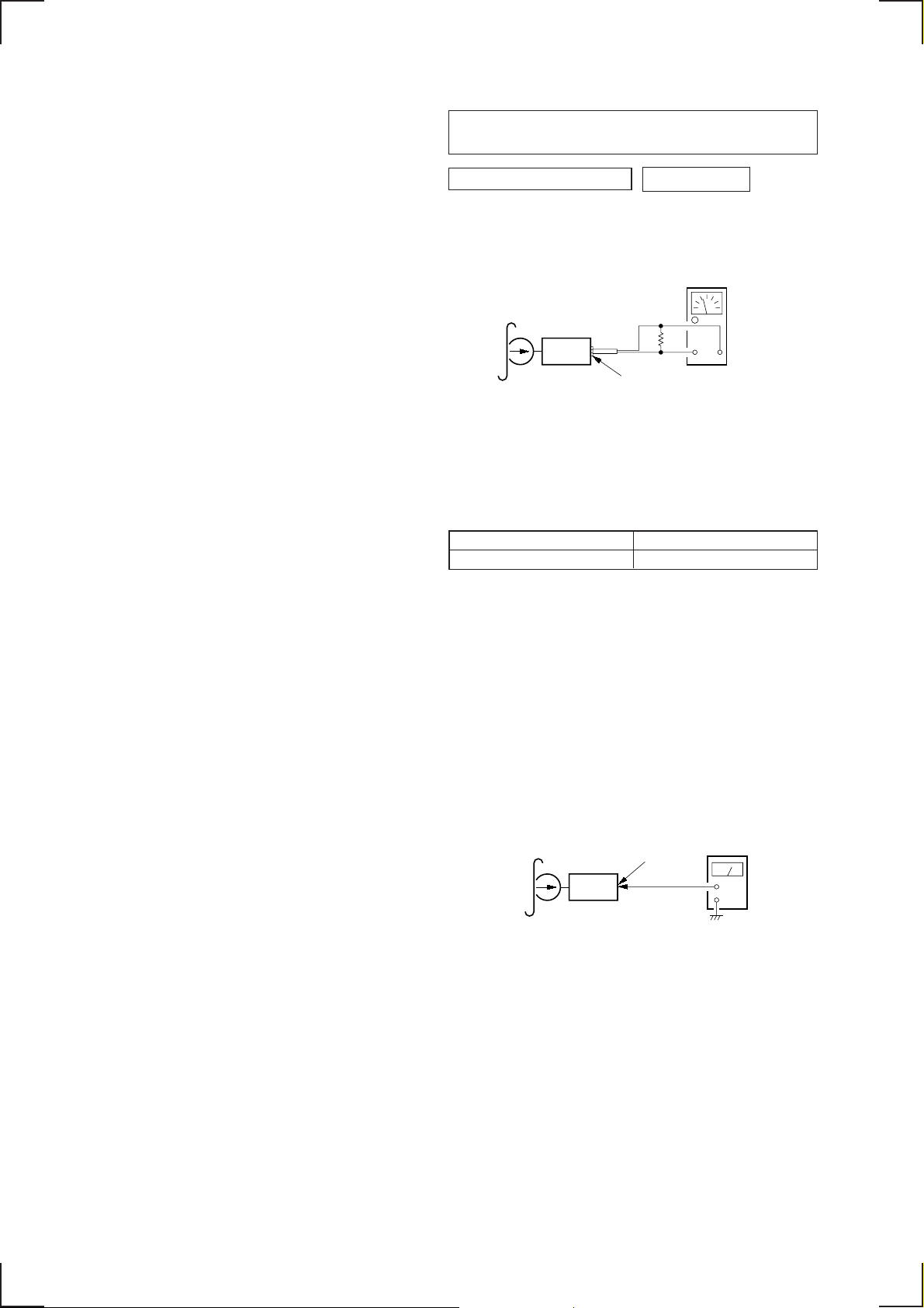
TAPE DECK SECTION
0 dB=0.775 V
Tape Speed Adjustment
Setting:
speed checker
or
test tape
WS-48A
(3 kHz, 0 dB)
LINE OUT REAR jack (CN780)
set
frequency counter
10 k
Ω
+–
Procedure:
1. Put the set into the FWD PB mode.
2. Adjust adjustment resistor for inside capstan motor so that the
reading on the speed checker or frequency counter becomes in
specification.
Specification: Constant speed
Speed checker Frequency counter
–1.5 to +2.5% 2,955 to 3,075 Hz
Adjustment Location: See page 22.
Dolby Level Adjustment
Setting:
[SHIFT] button : ON (light up SET UP and
PLAY MODE)
Preset [4] (PLAY MODE)
n [5] (n) buttons : NR off
SOUND (BAS) button : Center
SOUND (TRE) button : Center
SOUND (BAL) button : Center
SOUND (FAD) button : Center
SOUND (VOL) button : Maximum
Procedure:
1. Put the set into the FWD PB mode.
2. Adjust RV230 (L-CH) and RV240 (R-CH) so that the level
meter reading is –6±0.5 dB (0.37 to 0.41 V).
Adjustment Location: See page 22.
– 18 –
Page 19

TUNER SECTION
)
FM RF signal
generator
Carrier frequency : 98.00 MHz
Output level : 70 dB (3.2 mV)
Mode : stereo
Modulation : main: 1 kHz, 33.75 kHz deviation (45%)
sub : 1 kHz, 33.75 kHz deviation (45%)
: 19 kHz pilot: 7.5 kHz deviation (10%)
0.01 µF
set
antenna jack
+
–
LINE OUT REAR jack
(CN780)
level meter
10 k
Ω
0 dB=1 µV
Cautions during repair
When the tuner unit is defective, replace it by a new one because its internal block is difficult to repair.
Note: Adjust the tuner section in the sequence shown below.
1. FM Auto Scan/Stop Level Adjustment
2. FM Stereo Separation Adjustment (Wide)
3. FM Stereo Separation Adjustment (Narrow)
4. FM RDS S-Meter Adjustment
5. MW Auto Scan/Stop Level Adjustment
FM Auto Scan/Stop Level Adjustment
Setting:
[SOURCE] button : FM
FM RF signal
generator
Carrier frequency : 98.00 MHz
Output level : 22 dB (12.6
Mode : mono
Modulation : 1 kHz, 22.5 kHz deviation (30%
Procedure:
1. Set to the test mode. (See page 18)
2. Push the [SOURCE] button and set to FM.
Display
0.01 µF
antenna jack
µ
V)
set
FM Stereo Separation Adjustment (Wide)
Setting:
[SOURCE] button : FM
[SHIFT] button : ON (light up SET UP and
PLAY MODE)
Preset [4] (PLAY MODE)
n [5] (n) buttons : WIDE mode
Procedure:
FM Stereo
signal generator
output channel
L-CH L-CH A
R-CH L-CH Adjust RV3 on TUX10
R-CH R-CH C
L-CH R-CH Adjust RV3 on TUX10
Level meter Level meter
connection reading (dB)
B
for minimum reading.
D
for minimum reading.
SHUF
3. Push the preset [3] button.
Display
SHUF
4. Adjust with the v olume R V2 on TUX10 so that the “FM” indication turns to “FM0” indication on the display window.
But, in case of already indicated “FM0”, turn the RV2 so that
put out light “0” indication and adjustment.
Display
SHUF
L-CH Stereo separation: A-B
R-CH Stereo separation: C-D
The separations of both channels should be equal.
Specification: Separation more than 24 dB
Adjustment Location: See page 22.
Adjustment Location: See page 22.
– 19 –
Page 20

FM Stereo Separation Adjustment (Narrow)
Setting:
[SOURCE] button : FM
[SHIFT] button : ON (light up SET UP and
PLAY MODE)
Preset [4] (PLAY MODE)
n [5] (n) buttons : NARROW mode
FM RF signal
generator
Carrier frequency : 98.00 MHz
Output level : 70 dB (3.2 mV)
Mode : stereo
Modulation : main: 1 kHz, 20 kHz deviation (26.7%)
antenna jack
0.01 µF
set
sub : 1 kHz, 20 kHz deviation (26.7%)
: 19 kHz pilot: 7.5 kHz deviation (10%)
10 k
LINE OUT REAR jack
(CN780)
Procedure:
FM Stereo
signal generator
output channel
L-CH L-CH A
R-CH L-CH Adjust RV4 on TUX10
R-CH R-CH C
L-CH R-CH Adjust RV4 on TUX10
Level meter Level meter
connection reading (dB)
for minimum reading.
for minimum reading.
level meter
Ω
B
D
FM RDS S-Meter Adjustment
Setting:
[SOURCE] button: FM
FM RF signal
generator
0.01 µF
Carrier frequency : 98.00 MHz
Output level : 35 dB (56.2
Mode : mono
+
–
Procedure:
Modulation : no modulation
1. Set to the test mode. (See page 18)
2. Push the [SOURCE] button and set to FM.
Display
3. Push the
[10] button.
4. Adjust RV10 so that the display indication is “13.2”.
Display
SHUF
SHUF
antenna jack
µ
V)
set
L-CH Stereo separation: A-B
R-CH Stereo separation: C-D
The separations of both channels should be equal.
Specification: Separation more than 18 dB
Adjustment Location: See page 22.
Specification: Display indication: 13.0 to 13.4
Adjustment Location: See page 22.
– 20 –
Page 21

MW Auto Scan/Stop Level Adjustment
µ
Setting:
[SOURCE] n [MODE] buttons : MW
AM RF signal
generator
AM dummy antenna
(50 Ω)
Carrier frequency : 999 kHz
30% amplitude
modulation by
1 kHz signal
Output level : 33 dB (44.7
V)
30
Ω
15 pF
65 pF
set
antenna jack
Adjustment Location:
– SET UPPER VIEW –
Tape Speed Adjustment
TUX10
RV1 MW Auto Scan/Stop Level Adjustment
Procedure:
1. Set to the test mode. (See page 18)
2. Push the [SOURCE] button and set to FM.
3. Push the [MODE] button and set to MW.
Display
SHUF
TP
4. Push the preset
[3] button.
Display
SHUF
TP
5. Adjust with the volume RV1 on TUX10 so that the “MW”
indication turns to “MW0” indication on the display window.
But, in case of already indicated “MW0”, turn the R V1 so that
put out light “0” indication and adjustment.
RV240
(R-CH)
– SET BOTTOM VIEW –
RV230
(L-CH)
Dolby Level
Adjustment
RV2 FM Auto Scan/Stop Level Adjustment
RV3 FM Stereo Separation Adjustment (Wide)
RV4 FM Stereo Separation Adjustment (Narrow)
RV10 FM RDS S-Meter Adjustment
Display
SHUF
TP
Adjustment Location: See page 22.
– 21 –
TP (DOLBY-L)
TP (DOLBY-R)
– 22 –
Dolby Level
Adjustment
Page 22

XR-C8220R
7-1. BLOCK DIAGRAM – TUNER Section –
SECTION 7
DIAGRAMS
FM/AM
ANTENNA
FM/AM TUNER UNIT
TUX10
FM-ANT
2
1
AM-ANT
VCO (FM/AM)21FM-IF-COUNT11AM-IF-COUNT (SEEK)
LO/DX
4
6
9 16 13
15
LO/DX
FM OSC
AM OSC
+
VT (FM/AM)
5
IF IN
LOW-PASS
FILTER
Q17
FM/AM PLL
IC10
TIME CONSTANT
SWITCH
18 7
PD
IC11
FM B+
FORCED WIDE/
24
AM B+
WIDE/NARROW
SWITCH
Q15
NARROW
FM +B
NARROW
AM B+
D10
AM +B
AF SEEK SWITCH
Q16
WIDE/NARROW
SWITCH
Q14
9108
+B (FM/AM)
RECEIVE/SEEK
13
20SD22
ST/MONO
FM/AM SIGNAL
METER BUFFER
S-METER
19
Q13
RV10
FM RDS
S-METER
S-METER
(RDS)
15
FM L-OUT
FM R-OUT
AM-DET
FM-DET
BAND-PASS
FILTER
IC51
SWITCH
REGISTER
STATUS
IC50
MUTING
CONTROL SWITCH
Q51
7
3
ADPCM
ADDRESS
ANALYZER/
SYNTHESIZER
CONTROLLER
Q52
CONTROLLER
DATA I/O
TIMING
SADX
REGISTER
CONTROLLER
RWCK
OSC
CS1
CS2
TAS
SAS
WE
D-IN/
OUT
Q53
MUTING
Q60
AM/TIR SIGNAL SELECT
IC100
CONVERTER
ADIN
CONVERTER
D50
2 1
5 6
D/A
A/D
R-CH
18
16
R-CH
12
23
BUFFER
Q12
LIN
AM
ON
202619
FIN
L.P.F.
MUTING
Q50
TRAFFIC INFORMATION REPLAY
18
AOUT
17
FOUT
16
CPU INTERFACE
FM-L
A
(Page 27)
AM/TIR
B
(Page 27)
SERIAL REGISTER
IC101
40
41
39
37
36
46
50
44
17
CS
SAD
23
TAS
18
22
SAS
16
WE
2
RWCK
DIN
11
DOUT
15
• SIGNAL PATH
: FM
: AM (MW/LW)
XIN
X10
7.2MHz
XOUT
DOUT
DIN
61 520 4 2
252627 28
PLLSI
PLLSO
CLK
CE
PLLCE
PLLCKO
3
WIDE
2
1 53
20
4
SD-IN
AF-SEEK
SEEKOUT
ST-MONO
VSM
PDWN
35
TIR-PDOWN
XT
48
X100
4.19MHz
47
5
60
TIR-PLAY
TUNMUTE
96
TIR-RD
TIR-WR
BUSY
82 – 85
–
TIR-D0
TIR-D3
RESET
5355455
95
99
TIR-BUSY
100
TIR-RES
CE
11
56
TIR CE0
TIR CE1
RDS DECODER
IC150
PATH
SC
OUT
MPTH
SYSTEM CONTROLLER
18
2
CIN
19
X150
4.332MHz
52
MTP
IC600 (1/5)
CLOCKED
COMPARATOR
OSCILLATOR
& CLOCK
OSCI
OSCO
4
5
MPX
LVIN
57 kHz
BAND-PASS
FILTER
MULTI
DETECTOR
16
20
SIGNAL
QUALITY
DECODER
RDS/RDBS
DEMODULATOR
& DECODER
DAVN
8
75
DAVN
5
4
INTERFACE
REGISTER
IIC BUS
SLAVE
TRANSCEIVER
SDA
9
70
I2C SIO
SCL
10
71
I2C CKO
RDWRCE
TIR RD
TIR WR
TIR D0 –
97
TIR-CE0
D0 – D3
1 – 4
TIR D3
98
TIR-CE1
101
XT
05
– 23 – – 24 –
Page 23

7-2. BLOCK DIAGRAM – TAPE Section –
TAPE EQUALIZER AMP,
DOLBY NR AMP, AMS
(PLAYBACK)
FWD
L-CH
FWD
R-CH
REV
L-CH
REV
R-CH
HP901
R-CH
R-CH
FWD
IN (L)
34
32
REV
IN (L)
IC250
R-CH R-CH
FWD/REV
19
EQ AMP
MTL/NORMAL
18
EQ
OUT
29 27
RV230
DOLBY LEVEL (L)
R-CH
TAPE
IN (L)
XR-C8220R
LCH
R-CH
DOLBY
NR AMP
MUTE
+
MUTE/TAPE
17
NR.ON
16 20
R-CH
AMS
DET
AMS/PLAY
OUT
AMS
OUT
24
14
TAPE-L
C
(Page 27)
LOADING/TAPE
OPERATION
M901
(CAPSTAN/REEL)
REEL SENSOR B+
M
M
(METAL DETECT)
D200
113 102 116 114
N-ROUT
9
7
CAPSTAN/REEL
MOTOR DRIVE
MTLIN
3
VCC
OUT1
MOTOR
OUT2
DRIVE
LOADING/TAPE OPERATION
MOTOR DRIVE
IC201
Q204
IN1
IN2
BATT B+
LM-EJ
LM-LOD
110 109
2
4
Q250
MUTE SWITCH
REGULATOR
Q203
REGULATOR
CONTROL SWITCH
Q202
DOLBY
SYSTEM CONTROLLER
IC600 (2/5)
TAPEON
112
BATT B+
AMSON
CM-ON
111
103
AMSIN
POS0 – POS3
TAPE OPERATION
SWITCH
EJECT/FF/REW/
REV/FWD MODE DETECT
TAKE-UP
REEL
SENSOR
TAPE
DETECT
REEL SENSOR BOARD
104105 – 108
BUFFER
REEL
SUPPLY
SENSOR
REEL
05
Q201
– 25 –
• SIGNAL PATH
: TAPE PLAY
– 26 –
Page 24

XR-C8220R
7-3. BLOCK DIAGRAM – MAIN Section –
(Page 24)
(Page 24)
(Page 25)
CN780 (1/2)
BUS
AUDIO IN
L
R
A
B
C
FM-L
AM/TIR
TAPE-L
R-CH
R-CH
INPUT SELECT,
ELECTRICAL VOLUME
IC301
AUX-IN-L
42
FM-IN-L
40
AM-IN-L
39
TAPE-IN-L
41
36 – 38
VR
VOLUME
SUB CUT
SWITCH
Q360, 362
IN1
CONTROL
CIRCUIT
LOUDNESS
CONTROL
CIRCUIT
R-CH
INAO1 VOUT
INPUT
GAIN
33 32 31
SELECTOR
R-CH
D351 D350
REFERENCE VOLTAGE
GENERATOR (FOR BIAS)
IC302
ELECTRICAL VOLUME
(FOR SUBWOOFER)
IC350
BUFFER
INP1
INAO1
SHIFT
REGISTER &
LATCH
CLK
DATA
CLK
DATA
TONE
TIN1
30 26 25
VR
IN1
16
1720
ZC
DET
CE
78 9
SUBCE
CONTROL
CIRCUIT
VCT
BUFFER
VCT
COM +8V
R-CH
TCO1
VOLUME
CONTROL
CIRCUIT
OUT1
• SIGNAL PATH
: FM
: AM (MW/LW)
: TAPE PLAY
: BUS AUDIO IN
LINE DRIVER
IC310
FD
IN1
+
REGISTER &
15
FADER
CONTROL
CIRCUIT
SHIFT
LATCH
CLK
DATA
CLK
DATA
CE
2216 2117
VOLCE
FNTO1
REO1
24
23
2
7
IN1
IN2
BUFFER
IC383
OUT1
OUT2
13
12
R-CH
R-CH
R-CH
12
POWER AMP
IN2
IC700
MUTING
Q340
MUTING
Q430
MUTING
Q330
MUTING
Q440
MUTING
Q361
MUTING
Q461
OUT2+
OUT2–
(POWER CONNECTOR)
5
3
CN700 (1/2)
1
9
L
CN781 (1/2)
FRONT
LINE OUT
R
L
CN780 (2/2)
REAR
LINE OUT
R
L
CN781 (2/2)
SUB OUT
R
FRONT L (+)
FRONT L (–)
R-CH
BUFFER
IC320
CLK
DATA
VOLCE
SUBCE
62
61
CSV
IC650
SUB-SW1
SUB-SW0
23
AOUT
05
2 3
4.19MHz
XT
X650
NAR
RESET
XT
SD
SI
8
ST
22
2115
2214
23
117
917
CSV-SO
CSV-CKO
CSV-CE
CSV-NAR
CSV-RST
67
64
66
68
VOLCE
SUBCE
VOLSO/SUBSO
VOLCKO/SUBCKO
SYSTEM CONTROLLER
IC600 (3/5)
MUTE
DOLBC
TESTIN
TEL-ATT
65
115
58
79
MUTING
CONTROL SWITCH
Q700, 701
D717
POWER AMP
MUTE SWITCH
LEVEL SHIFT
– 27 – – 28 –
Q603
Q702
R-CH
R-CH
D715
21
IN4
14
11
IN1
15
IN3
22
MUTE
4
ST-BY
OUT4+
OUT4–
OUT1+
OUT1–
OUT3+
OUT3–
23
9
7
17
19
4
12
2
10
3
11
15
13
FRONT R (+)
FRONT R (–)
REAR L (+)
REAR L (–)
REAR R (+)
REAR R (–)
TEST MODE
TEL-ATT
Page 25

7-4. BLOCK DIAGRAM – DISPLAY/KEY CONTROL Section –
RE900
VOLUME/BASS/TREBLE/
BALANCE/FADER CONTROL
D510
J500
REMOTE IN
LSW900 – 918,
S900, SW801
D506
ROTARY
ENCODER
RE900
LED800
(TAPE WINDOW)
LED802
6
LED800, 802
XR-C8220R
LED801
TIR
48 72
RC-IN0
X1
93
X600
3.68MHz
RC-IN1
KEY ACTIVE
SWITCH
Q510, 511
35
AD-ON
LCD SO13LCD CKO
RE-IN1
76
KEYACK
46
47
KEYIN1
KEYIN0
X1A
73
X601
32.768kHz
X0A
74
X0
92
36 37
RE-IN0
14 16
LCD CE
LCD INH
32
BACKUP +5V
SYSTEM CONTROLLER
IC600 (4/5)
LSW900, 901, 903,
LSW904, 906 – 910,
LSW912 – 918
SW500
(NOSE DETECT)
80
NOSESW
LED DRIVE
Q901
BUZZER
DRIVE
Q601
15
BEEP
BZ600
(BUZZER)
LED DRIVE
Q900
LED DRIVE
Q501
59
LED900 – 907,
LSW902, 905, 911
PACK-IND
P-ON +10V
LCD +10V
LED DRIVE
Q502
31
TIR-IND
LCDANG
41
CONTRAST
SWITCHING
R952
OSC
21
OSC-OUT
05
20
OSC-IN
18
17
LCD-DATA
14
19
LCD-CE
LCD-CLK
LIQUID CRYSTAL DISPLAY DRIVER
LCD-INH
SEG101 – SEG165
IC900
26 – 90
LIQUID CRYSTAL DISPLAY
COM100 – COM107
LCD900
Q903
2
AMBER
100 – 93
1
GREEN
Q902
11 – 6
VLC0 – VLC5
Q508, 509
LCD +10V
– 29 –
– 30 –
Page 26

XR-C8220R
7-5. BLOCK DIAGRAM – BUS CONTROL/POWER SUPPLY Section –
SYSTEM CONTROLLER
IC600 (5/5)
CN600
BUS CONTROL IN
(FOR SONY BUS)
3
SIRCS
D604
BACKUP +5V
SIRCS BUFFER
Q602
BACKUP +5V
RESET SIGNAL
GENERATOR
IC500
REMOTE CONTROL
RECEIVER
IC901
D523
SW800
RESET
SONY BUS INTERFACE
IC602
RAM RESET
IC501
55
RAMBU
90
RESET
86
HSTX
24
SIRCS
POWSEL
56
S600
POWER SELECT
B (OFF)
A (ON)
TUNER ON +5V
(TUNER CIRCUIT B+)
+9V
(FOR VT)
+5V
REGULATOR
Q10
+9V
REGULATOR
Q11
(AUDIO CIRCUIT B+)
FM B+
(FM CIRCUIT B+)
AM B+
(AM CIRCUIT B+)
COM +8V
CN700 (2/2)
(POWER CONNECTOR)
D719
BATT B+
POWER AMP
8
ANT+B
STB
VCC
7
11
FM+B
REGULATOR
AM+B
COM8V
IC502
MODE1
23 4
MODE2
10
9
(IC700) B+
6
ANT REM
RESET
DATA
CLK
BUS ON
BATT
BATT B+
2
5
4
6
7
TH600
D606
2
6
4
1
3
D601
RST
DATA
CLK
BUS ON
OUT
BATT
SWITCH
BUS ON
SWITCH
BATTERY
SWITCH
BATTERY DETECT
RESET
DATA IN
DATA OUT
CLK IN
ON IN
BU IN
Q600
RST
BUS
13
9
8
11
12
10
11
18
17
19
10
77
SYSRST
UNISO
UNISI
UNICKO
BUS-ON
BU-IN
FM-ON
TU-ON
POWON
LEDON
DOORSW
ILL-ON
DIMMER
6
7
120
P-ON +10V
LCD +10V
REGULATOR
IC550, Q553
D532 – 534
BACKUP +5V
OSC
Q556
Q557
REGULATOR
CONTROL SWITCH
Q505
REGULATOR
CONTROL SWITCH
Q507
CURRENT
CONTROL SWITCH
Q554, 555
118
12
29
30
CN900
(FRONT PANEL SIDE)
10
D524
D525
EL900
(LCD BACK LIGHT)
CONTROL SWITCH
5
D553
Q503
POWER ON/OFF
SWITCHING
T550
INVERTER
TRANSFORMER
DIMMER
Q552
OSC OFF
SWITCH
+6V
REGULATOR
IC503
TH700
B+ SWITCH
Q703, 704
+10V
REGULATOR
Q504
+10V
REGULATOR
Q506
B+ SWITCH
Q550, 551
F701
5
16
7
14
AMP REM
BATT
ACC
ILL
CN500
(MAIN BODY SIDE)
ACC IN
81
05
ILL IN
78
ACCESSORY CHECK
Q705
D713
ILLUMINATION
LINE DETECT
Q512
– 31 – – 32 –
D507
Page 27

XR-C8220R
3.8 Vp-p
236 ns
7-6. NOTE FOR PRINTED WIRING BOARDS AND SCHEMATIC DIAGRAMS
Note on Printed Wiring Board:
• X : parts extracted from the component side.
• Y : parts extracted from the conductor side.
r
•
• b : Pattern from the side which enables seeing.
(The other layers' patterns are not indicated.)
Caution:
Pattern face side: Parts on the pattern face side seen from
(Conductor Side) the pattern face are indicated.
Parts face side: Parts on the par ts face side seen from
(Component Side) the parts face are indicated.
: Through hole.
Note on Schematic Diagram:
• All capacitors are in µF unless otherwise noted. pF: µµF
50 WV or less are not indicated except for electrolytics
and tantalums.
• All resistors are in Ω and 1/
specified.
¢
•
• C : panel designation.
• U : B+ Line.
• H : adjustment for repair.
• Power voltage is dc 14.4V and fed with regulated dc po wer
• Voltages and waveforms are dc with respect to ground
• Voltages are taken with a VOM (Input impedance 10 MΩ).
• Waveforms are taken with a oscilloscope.
• Circled numbers refer to waveforms.
• Signal path.
• Abbreviation
: internal component.
supply from ACC and BATT cords.
under no-signal (detuned) conditions.
no mark : FM
( ) : AM (MW/LW)
〈〈 〉〉 : TAPE PLA Y
Voltage variations may be noted due to normal production tolerances.
Voltage variations may be noted due to normal production tolerances.
F : FM
f : AM (MW/LW)
L : BUS AUDIO IN
E : TAPE PLAY
TAPE A : ENGLISH, FRENCH
TAPE B : ENGLISH, GERMAN
TAPE C : ENGLISH, SPANISH
TAPE D : ENGLISH, ITALIAN
4
W or less unless otherwise
• Waveforms
– MAIN Board –
1 IC10 @º (XOUT)
139 ns
2 IC100 $¶ (XT)
240 ns
3 IC150 4 (OSCO)
3.8 Vp-p
4.3 Vp-p
5 IC600 (£ (X1)
272 ns
6 IC650 2 (XT)
5.8 Vp-p
– KEY Board –
1 IC900 @º (OSC-IN)
µ
s
5.5
2 IC900 @¡ (OSC-OUT)
3.3 µs
– INVERTER Board –
1 Q556 (EMITTER)
2 Vp-p
6.8 Vp-p
230 ns
4 IC600 &¢ (X0A)
30.6
3.6 Vp-p
10 Vp-p
1.1 ns
3.6 Vp-p
µ
s
– 33 –
– 34 –
Page 28

XR-C8220R
7-7. PRINTED WIRING BOARD – MAIN Board (Component Side) –
• Semiconductor Location
(Component Side)
Ref. No. Location
D10 F-13
D200 H-4
D201 F-2
D202 F-3
D350 F-6
D351 F-6
D506 J-12
D508 B-9
D509 B-10
D510 C-9
D513 J-13
D514 K-13
D517 K-10
D519 K-10
D523 I-7
D524 J-4
D525 K-11
D526 K-10
D527 K-8
D528 K-6
D530 F-2
D601 E-2
D604 D-3
D605 D-2
D606 D-2
D701 C-7
D702 B-7
D703 B-7
D704 B-6
D705 B-7
D712 D-4
D715 B-5
D717 D-7
D718 C-3
D719 C-3
IC10 F-11
IC11 E-12
IC50 J-11
IC51 I-11
IC100 J-7
IC101 J-9
IC201 G-3
IC250 H-11
Ref. No. Location
IC301 G-8
IC302 F-10
IC310 D-12
IC320 G-7
IC350 E-7
IC383 D-8
IC410 D-10
IC500 D-5
IC600 H-5
IC602 D-2
IC650 E-4
Q11 E-9
Q14 G-13
Q15 G-12
Q16 E-12
Q17 E-12
Q50 I-12
Q51 J-12
Q60 I-12
Q80 I-12
Q201 F-3
Q202 G-3
Q250 H-10
Q330 B-12
Q340 B-11
Q361 B-10
Q430 B-11
Q440 B-12
Q461 B-10
Q502 K-10
Q507 K-6
Q508 K-10
Q509 K-9
Q510 J-11
Q511 J-12
Q600 E-2
Q602 D-3
Q603 E-5
Q700 B-9
Q702 D-7
Q703 D-4
Q704 D-5
– 35 – – 36 –
Page 29

7-8. PRINTED WIRING BOARD – MAIN Board (Conductor Side) –
• Semiconductor Location
(Conductor Side)
Ref. No. Location
D11 E-10
D12 E-10
D50 J-12
D501 K-7
D502 K-6
D503 K-10
D504 K-7
D507 F-4
D512 J-12
D515 J-12
D516 J-12
D518 J-12
D520 J-12
D521 K-10
D522 J-12
D532 E-2
D533 E-2
D534 E-2
D550 I-1
D602 B-1
D603 B-1
D608 B-1
D706 C-6
D707 C-6
D708 C-6
D709 D-2
D710 B-3
D711 B-9
D713 E-4
D714 E-3
D716 B-9
XR-C8220R
IC150 J-9
IC501 D-6
IC502 E-1
IC503 G-1
IC700 A-7
Q10 F-10
Q12 I-14
Q13 I-14
Q52 I-11
Q53 I-11
Q203 G-3
Q204 G-3
Q360 E-6
Q362 E-6
Q460 E-6
Q462 E-6
Q501 J-7
Q503 J-4
Q504 K-6
Q505 J-6
Q506 K-6
Q512 F-5
Q550 H-3
Q551 I-4
Q601 I-3
Q701 C-9
Q705 E-4
(Page 51)
(Page 51)
– 37 –
(Page 51)
(Page 51)
– 38 –
Page 30

XR-C8220R
7-9. SCHEMATIC DIAGRAM – MAIN Board (1/4) – • See page 34 for Waveforms. • See page 53 for IC Block Diagrams.
(Page
41)
(Page
45)
– 39 – – 40 –
(Page 44)
Page 31

7-10. SCHEMATIC DIAGRAM – MAIN Board (2/4) – • See page 55 for IC Block Diagrams.
(Page
40)
XR-C8220R
(Page
44)
– 41 –
(Page 46)
– 42 –
Page 32

XR-C8220R
7-11. SCHEMATIC DIAGRAM – MAIN Board (3/4) – • See page 34 for Waveforms. • See page 54 for IC Block Diagrams.
(Page 40)
(Page
41)
(Page
45)
– 43 – – 44 –
Page 33

7-12. SCHEMATIC DIAGRAM – MAIN Board (4/4) – • See page 56 for IC Block Diagrams.
(Page
40)
XR-C8220R
(Page 42)
(Page
44)
(Page 52)
(Page 52)
(Page
52)
(Page 52)
– 45 –
– 46 –
Page 34

XR-C8220R
7-13. PRINTED WIRING BOARD – KEY Board –
• Semiconductor
Location
(Component Side)
Ref. No. Location
IC901 C-4
LED900 C-4
LED901 A-4
LED902 A-2
LED903 A-2
LED904 C-2
LED905 C-2
LED906 B-2
LED907 B-2
• Semiconductor
Location
(Conductor Side)
Ref. No. Location
D901 C-5
D903 B-10
IC900 B-9
Q900 B-11
Q901 B-11
Q902 B-10
Q903 B-10
(Page 51)
– 47 – – 48 –
Page 35

7-14. SCHEMATIC DIAGRAM – KEY Board – • See page 34 for Waveforms.
XR-C8220R
(Page 52)
– 49 –
– 50 –
Page 36

XR-C8220R
7-15. PRINTED WIRING BOARDS – SUB/INVERTER Boards –
7-16. SCHEMATIC DIAGRAM – SUB/INVERTER Boards – • See page 34 for Waveform.
(Page 38) (Page 48)
(Page 46)
(Page 49)
(Page 38)
(Page 37)
(Page 46)
(Page 46)
(Page 38)
(Page 46)
– 51 – – 52 –
Page 37

• IC Block Diagrams
– MAIN Board –
IC10 BU2624FV-E2
CTL
I/O
REFERENCE
DIVIDER
SHIFT REGISTER LATCH
XIN
1
2
CE
CK
4
DA
5
CD
6
7
P0
9
P1
10
P3
MAIN
COUNT
PRESCALER
IF COUNT
CTL
20BIT COUNT
PHASE
DET
XOUT
20
19
VSS
18
PD
17
VDD
FMIN
16
AMIN
15
P2
14
13
IFIN
12
SD
P4
11
IC100 MSM6688GS-2K
CEWRRD
RESET
5253545556
1
D0
2
BUSY
RPM
VPM
ACON
TEST
MCUM
TEST
TEST
TEST
D1
3
D2
4
D3
5
6
7
8
9
10
CE
11
12
13
14
MCU I/F
STATUS
REGISTER
TEST
CIRCUIT
12BIT
ADC
NAR
MON
51 46
TIMING
CONTROLLER
LPF
RWCK
DVDDXTXT
OSC
ADDRESS
CONTROLLER
ADPCM
ANALYZER/
SYNTHESIZER
12BIT
DAC
SG
CIRCUIT
WE
DROM
DATA
I/O
DI/0
+
REGISTER
CONTROLLER
-
CS4
43444547484950
42
CS3
41
CS2
40
CS1
39
SADX
SADY
38
37
TAS
36
SAS
35
PDWN
34
TEST
33
TEST
RSEL2
32
RSEL1
31
30
DGND
29
AGND
-
+
15 16 17 18 19 20 21 22 23 24 25 26 27 28
TEST
ADIN
FOUT
AOUT
FIN
AMON
DVDD
AVDD
SG
SGC
LOUT
LINE
MOUT
– 53 –
MIN
Page 38

IC101 MSM6684JSDR1
TEST
RWCK
TEST
TEST
TEST
TEST
DIN
VSS
1
2
NC
3
4
5
9
10
11
NC
12
13
I/O CONTROL
WRITE CLOCK
GENERATOR
TIMING
GENERATOR
8,388,608DATA
REGISTER
COLUMN DECODER
COLUMN ADDRESS
COUNTER
ROW
DECODER
ADDRESS
MULTIPLEXER
REFRESH TIMER
REFRESH ADDRESS
COUNTER
ROW ADDRESS
COUNTER
ROW ADDRESS
REGISTER
26
VCC
25
RS/A
24
RFSH
SAD
23
22
SAS
18
TAS
CS
17
WE
16
DOUT
15
14
NC
IC150 SAA6588T-118
SCOUT
CIN
LVIN
20
MULTI
PATH
DETECTOR
2
1
MRO
MPTH
CLOCKED
COMPARATOR
RDS/RDBS
DEMODULATOR
TEST
CONTROL
3
19
TCON
18
BAND-PASS FILTER
OSCILLATOR
& CLOCK
4 5
OSCO
57kHz
8th ORDER
RDS/RDBS
DECODER
6
OSCI
VSSD
CLOCK
DATA
VDDD
VREF
17
87
DAVN
MPX
POWER SUPPLY
SIGNAL QUALITY
DECODER
445
INTERFACE
REGISTER
VSSA
15
& RESET
VDDA
14
CLOCK
DATA
IIC BUS SLAVE
TRANSCEIVER
9 10
SDA
AFIN
1316
PAUSE
DETECTOR
SCL
IC201 LB1638M
10
1
MAD
PSWN
11
12
GND
2
IN1
VCC
3
4
IN2
5 6
GND
CONTROL LOGIC
N.C.
9
OUT1
VS
8
7
OUT2
N.C.
– 54 –
Page 39

IC250 CXA2510AQ-T4
PBEQ1
PBOUT1
GND
120µ/
70µ
+
–
PBFB1
31
32
PBRIN1
1
VCT
PBEQ2
F2
F1
–
+
120µ/
70µ
345 6 7 8 9 10
2
VCC
PBOUT2
PBREF1
PBFIN1
VCT
PBGND
PBFIN2
PBREF2
PBRIN2
PBFB2
33
34
35
36
37
38
39
40
TAPEIN1
X1
+
X1
TAPEIN2
AUXIN1
T1
AUXIN2
DIREF
2425
T2
LPF
MSLPF
NR BIAS
TAPE/AUX
TAPE EQ
FWD/RVS
VCC
+
–
F3
–
+
LINEOUT2
+
OFF/B
NR
–
TCH2
2122232627282930
NR
OFF/B
MS
MODE
NR
MODE
DETECT
NC
PLAY
MS ON/
OFF
20
19
18
17
16
15
14
13
12
11
MSMODE
DRSW
TAPESW
INSW
NRSW
NC
MSOUT
DGND
MSTC
FF
MSSW
NC
TCH1
LINEOUT1
IC301 CXA1946BQ-T6
GAIN12
GAIN11
IN14
IN13
IN12
IN11
IN21
IN22
IN23
IN24
GAIN21
GAIN22
GAIN134
36
37
38
39
40
41
42
43
44
45
46
47
48
INPUT SW
ZCDET
INPUT SW
LDLC134LDHC133INAO132VRIN1
35
LOUD
LOUD
VOLUME
8dB STEP
LATCH
SHIFT
REGISTER
VOLUME
8dB STEP
VOUT130TIN129TCLC128TCLC1127TCLC1226TCO125FDIN1
31
VOLUME
1dB STEP
VCTBUFF
VCTBUFF
VCTBUFF
LATCH
CONTROL
VCTBUFF
VCTBUFF
VCTBUFF
VOLUME
1dB STEP
TONE FADER
TONE FADER
45k
45k
24
23
22
21
20
19
18
17
16
15
14
13
FNTO1
REO1
CE
CLK
DGND
GND
VCC
VCT
DATA
TIMER
REO2
FNTO2
1
GAIN234
2
3
LDLC2
LDHC2
4
INAO25VRIN2
6
VOUT2
7
8
9
11
12
TIN2
TCLC2
TCLC2110TCLC22
TCO2
FDIN2
– 55 –
Page 40

IC310, 410 TDA8574 (T)
1
VCCL
2
INL
SVRL
3
BUFFER
BUFFER
VCCL
LIFT
AMP
IC350 CXA1846BN-T4
VRIN 1
OUT 1
N.C.
GND
INP 1
INN 1
VCT 1
20 19 18 17 16 15 14 13 12 11
CL+
16
CL–
15
–
+
INAO 1
8dB STEP
VOLUME
1dB STEP
VOLUME
VCT
VCC
REFERENCE
4
INML
INMR
5
REFERENCE
SVRR
INR
VCCR
6
7
8
BUFFER
BUFFER
IC502 BA3918-V3
VCCL
VCCR
VCCR
SIGNAL
AMP
SIGNAL
AMP
LIFT
AMP
VCT 2
LATCH
CONTROL
INAO 2
8dB STEP
VOLUME
LGND
14
OUTL
13
12
OUTR
RGND
11
CR–
10
9
CR+
LATCH
SHIFT
REGISTER
+
–
1 2 3 4 5 6 7 8 9 10
INP 2
INN 2
VRIN 2
ZC
DET
1dB STEP
VOLUME
OUT 2
CE
DATA
VCT
BUFFER
CLK
INIT
IC602 BA8270F-E2
BUS ON
1
REGULATOR
OVER VOLTAGE
PROTECT
–
+
2 3
4
1
NC
STB
MODE2
MODE1
5 6 7 8 9 10 1211
VCC
AMP
ANT
COM
VDD
–
+
AM
–
+
FM
–
+
GND
2
RST
BATT
3
4
CLK
5
VREF
6
DATA
GND
7 8
BUS ON
SWITCH
RESET
SWITCH
BATTERY
SWITCH
14
13
12
11
10
9
VCC
RST
BUS ON
CLK IN
BU IN
DATA IN
DATA OUT
– 56 –
Page 41

IC650 MSM6656A-687GS-KR1 (TYPE A)
IC650 MSM6656A-688GS-KR1 (TYPE B)
IC650 MSM6656A-689GS-KR1 (TYPE C)
IC650 MSM6656A-690GS-KR1 (TYPE D)
1
VDD
2
XT
3
CMD
XT
NC
4
OSC
5
NC
6
7
NC
8
ST
TIMMING
CONTROLLER
I/O
INTERFACE
17 BIT
ADDRESS
COUNTER
BEEP TONE
GENARATOR
MELODY
GENARATOR
DATA
CONTROLLER
LPF
12 BIT
DAC
12
PCM
SYNTHSIZER
ADPCM
SYNTHESIZER
24
GND
23
AOUT
22
NAR
21
NC
20
BUSY
19
NC
18
NC
17
RESET
12/PoRT0
13/PoRT1
1M BIT ROM
17 BIT
MULTIPLEXER
7
9
10
10
11
11
12
ADDRESS
&
COMMAND
CONTROLLER
EDITING ROM &
ADDRESS ROM
CONTAINS 22KBIT
8
16
CH
15
16/SD
15/SI
14
14
13
– 57 –
Page 42

7-17. IC PIN FUNCTION DESCRIPTION
• MAIN BOARD IC600 MB90574PFV-G-209-BND (SYSTEM CONTROLLER)
Pin No. Pin Name I/O Function
Seek control signal output to the FM/AM tuner unit (TUX10)
1 SEEKOUT O
2 AF-SEEK O
3
4 ST-MONO I/O
5 TUNMUTE O
6
7
8 VCC —
9
10 BUS-ON
11 SYSRST O
12 DOORSW I
13 LCD SO
14 LCD CKO
15
16 LCD CE
17 UNISI
18 UNISO
19 UNICKO
20 SD-IN
21
22
23
24
25 PLLSI I
26 PLLSO O
27 PLLCKO O
28 PLLCE O
29
WIDE
FM-ON O
TU-ON O
CSV-RST
BEEP O Beep sound drive signal output terminal
CSV-SO
CSV-CKO
CSV-CE
SIRCS
ILL-ON O
AM mode: Used for IF count output/SD output request/AGC cut at SEEK or BTM
FM mode: Used for SD speed up at SEEK, BTM, or AF
“L” is output at tuner off
PLL low-pass filter time constant selection signal output at AF SEEK
“H” is output when AF SEEK
IF band select signal output to the FM/AM tuner unit (TUX10) “H”: wide mode
In receiving FM signals, interference noise from adjacent stations is removed by narrowing the
O
IF band automatically in the tuner unit so as to raise the selectivity, but in this case, the distortion
may increase and accordingly, the IF band is widened forcibly
FM stereo broadcasting detection signal input from the FM/AM tuner unit (TUX10), or forced
monaural control signal output to the FM/AM tuner unit (TUX10)
“L” is input in the FM stereo mode, or “L” is output in the forced monaural mode
Muting on/off control signal output of the FM and AM tuner signal “H”: muting on
FM system power supply on/off control signal output to the BA3918 (IC502)
“L”: AM power on, “H”: FM power on
Tuner system power supply on/off control signal output to the BA3918 (IC502)
“H”: tuner power on
Power supply terminal (+5V)
O
Reset signal output to the CSV (IC650) “L”: reset
O Bus on/off control signal output to the SONY bus interface (IC602) “L”: bus on
Reset signal output to the SONY bus interface (IC602) “L”: reset
Front panel open/close detection signal input “L” is input when the front panel is closed
O Serial data output to the liquid crystal display driver (IC900)
O Serial data transfer clock signal output to the liquid crystal display driver (IC900)
O Chip enable signal output to the liquid crystal display driver (IC900) “H” active
I Serial data input from the SONY bus interface (IC602)
O Serial data output to the SONY bus interface (IC602)
O Serial data transfer clock signal output to the SONY bus interface (IC602)
Station detector detect input from the FM/AM tuner unit (TUX10)
I
Stop level for SEEK, BTM, etc. is determined SD is present at input of “H”
O
Serial data output to the CSV (IC650)
O
Serial data transfer clock signal output to the CSV (IC650)
O
Chip enable signal output to the CSV (IC650) “L” active
I
Sircs remote control signal input from the remote control receiver (IC901)
PLL serial data input from the FM/AM PLL (IC10)
PLL serial data output to the FM/AM PLL (IC10)
PLL serial data transfer clock signal output to the FM/AM PLL (IC10)
PLL chip enable signal output to the FM/AM PLL (IC10) “H” active
Power on/off control signal output of the illumination LED and liquid crystal display driver
(IC900) “H”: power on Depends on initial setting of power select switch (S600)
Power select switch (S600) on: “H” output at the accessory on
Power select switch (S600) off: “H” output at the power on
30 DIMMER I/O
31 TIR-IND O
Dimmer control in/out terminal
At initial mode: The presence of dimmer select function is set (if this status, if “L” is input, the
dimmer select function is present)
At normal mode: LCD back light brightness control signal output
LED drive signal output of the TIR indicator (LED801) “H”: LED on
– 58 –
Page 43

Pin No. Pin Name I/O Function
32 LCD INH O
33
34 C —
35 AD-ON
36 RE-IN0
37 RE-IN1
38 DVCC —
39 DVSS —
40 — I
41 LCDANG
42 AVCC —
43 AVRH
44 AVRL
45 AVSS —
46 KEYIN0
47 KEYIN1
48 RC-IN0
49 DSTSEL0 I
50 DSTSEL1 I
51 DSTSEL2
52 MTP
53
54 VCC —
55 RAMBU I
56 POWSEL
57 EQ-SEL I
58 TESTIN
59 PACK-IND
60 TIR-PLAY O
61 SUB-SW1 O
62 SUB-SW0 O
63 VSS —
64 VOLCE
65 MUTE
66
67
68 SUBCE
VSS
VSM I
VOLSO/
SUBSO
VOLCKO/
SUBCKO
Blank indicate control signal output to the liquid crystal display driver (IC900) “L”: no display
—
Ground terminal
Connected to coupling capacitor for the power supply
A/D converter power control signal output terminal
O
When the KEYACK (pin &§) that controls reference voltage power for key A/D conversion input
is active, “L” is output from this terminal to enable the input
I
Dial pulse input of the rotary encoder (RE900)
(for VOLUME/BASS/TREBLE/BALANCE/FADER control)
I
Power supply terminal (+5V) (for D/A converter)
Ground terminal (for D/A converter)
Not used (fixed at “L”)
View field angle control signal is output when front panel is fully opened
O
“H”: front panel is fully opened
Power supply terminal (+5V) (for A/D converter)
I Reference voltage (+5V) input terminal (for A/D converter)
I Reference voltage (0V) input terminal (for A/D converter)
Ground terminal (for A/D converter)
Key input terminal (A/D input) (LSW900, S900, LSW901 to LSW908) OFF, SEEK/AMS +
I
+ ) = 0 – , MODE *, SOURCE, SOUND, DSPL, SHIFT, 1, 2, 3 keys input
Key input terminal (A/D input) (SW801, LSW909 to LSW918)
I
6, LIST, AF/TA, PTY LIST, 10, 9, 8, 7, 6, 5, 4 keys input
I Rotary remote commander key input terminal (A/D input)
Destination setting terminal (fixed at “L”)
Destination setting terminal (fixed at “H”)
Destination setting terminal (Type 1: fixed at “L”, Type 2: fixed at 1/4 voltage, Type 3: fixed at
I
1/2 voltage, Type 4: fixed at 3/4 voltage)
I Multi-path detection signal input from the RDS decoder (IC150)
FM and AM signal meter voltage detection input from the FM/AM tuner unit (TUX10)
(A/D input)
Power supply terminal (+5V)
Internal RAM reset detection signal input from the RN5VD33AA (IC501)
Input terminal to check that RAM data are not destroyed due to low voltage
This checking is made within 100 msec after reset
I Power select switch (S600) input terminal “L”: off (halt mode), “H”: on (operation mode)
Not used (fixed at “H”)
I Setting terminal for the test mode “L”: test mode, Normally: fixed at “H”
LED drive signal output of the tape window illumination and 6 indicators (LED800, 802)
O
“H”: LED on “H” is output to turn on LED when front panel is opened
AM/TIR selection signal output to the TC4W66F (IC51) “L”: AM signal, “H”: TIR signal
Sub woofer output cut-off frequency select signal output terminal
Sub woofer output cut-off frequency select signal output terminal
Ground terminal
O Chip enable signal output to the main electrical volume (IC301) “H”: active
O Audio line muting on/off control signal output terminal “H”: muting on
O Serial data output to the main electrical volume (IC301) and sub electrical volume (IC350)
Serial data transfer clock signal output to the main electrical volume (IC301) and sub electrical
O
volume (IC350)
O Chip enable signal output to the sub electrical volume (IC350) “H” active
– 59 –
Page 44

Pin No. Pin Name I/O Function
69
70 IIC SIO I/O
71 IIC CKO O
72 RC-IN1
73 X1A O
74 X0A I
75 DAVN I
76 KEYACK
77 BU-IN
78 ILL IN
79
80 NOSESW I
81 ACC IN
82 to 85
86 HSTX I
87 MD2 I
88 MD1 I
89 MD0 I
90 RESET I
91 VSS —
92 X0
93 X1
94 VCC —
95 TIR-BUSY I
96 TIR-WR O
FLASH-W
TEL-ATT I Telephone muting signal input terminal At input of “H”, the signal is attenuated by –20 dB
TIR-D0 to TIR-D3
Internal flash memory data write mode detection signal input terminal “L”: data write mode
I
Not used (fixed at “H” in this set)
Two-way data bus with the RDS decoder (IC150)
Bus clock signal output to the RDS decoder (IC150)
I Rotary remote commander shift key input terminal “L”: shift
Sub system clock output terminal (32.768 kHz)
Sub system clock input terminal (32.768 kHz)
Data transmit completed detect signal input from the RDS decoder (IC150) “H” active
Input of acknowledge signal for the key entry Acknowledge signal is input to accept function
I
and eject keys in the power off status On at input of “H”
Battery detect signal input from the SONY bus interface (IC602) and battery detect circuit
I
“L” is input at low voltage
Auto dimmer control illumination line detection signal input terminal
I
“L” is input at dimmer detection
Front panel block remove/attach detection switch (SW500) input terminal
“L”: front panel is attached
I Accessory detect signal input terminal “L”: accessory on
I/O
Two-way data bus with the MSM6688GS (IC100)
Hardware standby input terminal “L”: hardware standby mode Reset signal input in this set
Setting terminal for the CPU operational mode (fixed at “L” in this set)
Setting terminal for the CPU operational mode (fixed at “H” in this set)
Setting terminal for the CPU operational mode (fixed at “H” in this set)
System reset signal input from the reset signal generator (IC500) and reset switch (SW800)
“L”: reset “L” is input for several 100 msec after power on, then it changes to “H”
Ground terminal
I Main system clock input terminal (3.68 MHz)
O Main system clock output terminal (3.68 MHz)
Power supply terminal (+5V)
Busy detection signal input from the MSM6688GS (IC100)
“H” is output while MSM6688GS (IC100) is executing a command
Data write strobe signal output to the MSM6688GS (IC100)
“L” is output when data (D0 to D3) are output to the MSM6688GS (IC100)
97 TIR-CE0 O
98 TIR-CE1 O
99 TIR-RES O
100 TIR-PDOWN O
101 TIR-RD O
102 MTLIN I
103 AMSIN I
104 REEL I
105 POS0 I
106 POS1 I
107 POS2 I
108 POS3 I
Chip enable signal output to the MSM6688GS (IC100)
TIR-WR (pin (§) or TIR-RD (pin `⁄‚⁄) is accepted when CE is “L” or CE is “H” respectively
TIR-WR (pin (§) or TIR-RD (pin `⁄‚⁄) is not accepted when CE is “H” or CE is “L” respectively
Reset signal output to the MSM6688GS (IC100) “H”: reset
Power down control signal output to the MSM6688GS (IC100) “L”: power down
Data read strobe signal output to the MSM6688GS (IC100)
“L” is output when data (D0 to D3) are output to the MSM6688GS (IC100)
Metal detection signal input terminal “L”: normal position, “H”: metal position
Whether a music is present or not from CXA2510AQ (IC250) is detected at auto music sensor
“L”: music is present, “H”: music is not present
Rotation detect signal input from supply reel sensor and take-up reel sensor on the deck
mechanism
Tape position (EJECT/FF/REW/
REV/FWD mode) detect input from
the tape operation switch on the deck
mechanism
POS0: “L”: EJECT mode, “H”: others mode
POS1: “L”: FF and FWD mode, “H”: others mode
POS2: “L”: REW mode, “H”: others mode
POS3: “L”: REV and EJECT mode, “H”: others mode
– 60 –
Page 45

Pin No. Pin Name I/O Function
109 LM-EJ O
110 LM-LOD O
111 CM-ON O
112 TAPEON O
113 N-ROUT O
114 AMSON O
115 DOLBC O
116 DOLBY I/O
117
118 LEDON
119 VSS
120 POWON
CSV-NAR
Motor drive signal output to the loading/tape operation motor drive (IC201) “H” active
(For the eject direction and reverse side operation) *1
Motor drive signal output to the loading/tape operation motor drive (IC201) “H” active
(For the loading direction and forward side operation) *1
Capstan/reel motor (M901) drive signal output terminal “H”: motor on
Tape system power supply on/off control signal output terminal “H”: tape on
Forward/reverse direction control signal output to the CXA2510AQ (IC250)
“L”: forward direction, “H”: reverse direction
Tape auto music sensor control signal output to the CXA2510AQ (IC250)
“L” is output to lower the gain for audio level at FF/REW mode
Standby on/off control signal output to the power amplifier (IC700)
“L”: standby mode, “H”: amp on
Dolby control in/out terminal
At initial mode: valid/invalid selection input of dolby function (valid at “L” input)
At normal mode: dolby on/off control signal output to the CXA2510AQ (IC250)
(dolby on at “H” output)
I
“H” is input when CSV (IC650) sends data
O Power supply on/off control signal output of the illumination LED “H”: power on
—
Ground terminal
O Main system power supply on/off control signal output to the BA3918 (IC502) “H”: power on
*1 Loading/tape operation motor control
Mode
Terminal
LM-LOD (pin `⁄⁄‚)
LM-EJ (pin `⁄‚·)
STOP
“L” “H” “L” “H”
“L” “L” “H” “H”
LOADING/
FORWARD
EJECT/
REVERSE
BRAKE
– 61 –
Page 46

SECTION 8
EXPLODED VIEWS
NOTE:
• -XX and -X mean standardized parts, so they
may have some difference from the original
one.
• Color Indication of Appearance Parts
Example:
KNOB, BALANCE (WHITE) . . . (RED)
↑↑
Parts Color Cabinet's Color
(1) CHASSIS SECTION
not
supplied
MG-25D-136
13
14
• Items marked “*” are not stocked since they
are seldom required for routine service. Some
delay should be anticipated when ordering
these items.
• The mechanical parts with no reference number in the exploded views are not supplied.
• Hardware (# mark) list and accessories and
packing materials are given in the last of the
electrical parts list.
17
LUG1
16
19
18
A
15
not
supplied
16
23
21
• Abbreviation
TYPE A : ENGLISH, FRENCH
TYPE B : ENGLISH, GERMAN
TYPE C : ENGLISH, SPANISH
TYPE D : ENGLISH, ITALIAN
F701
22
#2
16
16
27
#3
24
25
26
28
12
11
10
9
7
31
4
3
8
5
#1
#2
#1
#2
2
Front panel section
Ref. No. Part No. Description Remark
1 3-022-310-01 COLLAR
2 X-3375-093-3 PANEL ASSY, SUB
3 3-022-338-01 BUTTON (EJECT) (6)
* 4 1-669-656-12 SUB BOARD
5 X-3375-068-1 LOCK ASSY
* 6 3-022-307-01 INSULATED PLATE
7 3-935-003-01 SPRING (C DOOR), TORSION
8 3-027-799-11 DOOR, CASSETTE
9 3-713-786-51 SCREW +P 2X3
10 3-953-235-01 DAMPER, OIL
1
#3
#3
#3
not
supplied
6
20
A
#3
#3
B
#3
29
#3
30
Ref. No. Part No. Description Remark
* 17 A-3317-692-A MAIN BOARD, COMPLETE (TYPE D)
* 17 A-3317-694-A MAIN BOARD, COMPLETE (TYPE A)
* 18 3-011-078-01 BRACKET (POWER IC)
* 19 3-022-317-01 BRACKET (AMP)
* 20 3-022-306-01 HEAT SINK
* 21 3-355-209-01 PLATE (B), GROUND
22 1-776-527-71 CORD (WITH CONNECTOR) (ISO) (POWER)
* 23 3-023-774-01 PLATE (LOCK), GROUND
24 3-937-282-03 CASE (UPPER)
* 25 3-034-264-01 SHEET (E)
B
11 3-341-752-11 WASHER, POLYETHYLENE
12 3-011-170-01 GEAR (HOLDER)
13 X-3375-066-2 BRACKET (GEAR) ASSY
* 14 3-022-316-01 COVER
15 3-919-171-01 SCREW (2.6X6) (C TIGHT)
16 3-915-923-01 SCREW, GROUND POINT
* 17 A-3317-686-A MAIN BOARD, COMPLETE (TYPE C)
* 17 A-3317-690-A MAIN BOARD, COMPLETE (TYPE B)
* 26 A-3313-646-A INVERTOR BOARD, COMPLETE
27 1-783-495-11 CORD (WITH CONNECTOR) (EL)
28 3-937-812-03 CASE (LOWER)
29 1-777-246-11 CORD (WITH CONNECTOR) (ANT)
* 30 X-3375-081-1 CHASSIS ASSY
* 31 3-025-352-01 PLATE (INV), SHIELD
F701 1-532-877-11 FUSE (BLADE TYPE) (AUTO FUSE) (10A)
* LUG1 1-537-738-21 TERMINAL, EARTH
– 62 –
Page 47

(2) FRONT PANEL SECTION
53
54
55
56
71
67
66
65
64
63
52
51
62
61
60
59
58
57
68
69
#4
not supplied
(KEY board)
not supplied
LCD900
EL900
68
70
70
70
Ref. No. Part No. Description Remark
51 X-3377-531-1 PANEL SUB ASSY, FRONT
52 3-022-332-01 BUTTON (10 KEY)
53 3-022-329-21 BUTTON (SOURCE)
54 3-033-667-02 KNOB (VOL)
55 3-022-323-24 LEVER (SHUTTLE)
56 3-022-324-02 PLATE (SHUTTLE), LIGHT GUIDE
57 3-022-330-01 BUTTON (MODE) (MODE *. OFF)
58 3-030-648-01 PLATE (RING), LIGHT GUIDE
59 3-022-331-01 BUTTON (SOUND) (SOUND. DSPL)
60 3-932-225-01 SPRING (OPEN)
61 3-022-333-01 BUTTON (OPEN)
(+ + ) . = 0 –. SEEK/AMS)
(SHIFT. 1. 2. 3. 4. 5. 6. 7. 8. 9. 10)
Ref. No. Part No. Description Remark
62 3-022-308-12 BUTTON (PTY) (PTY. AF/TA. TIR)
* 63 3-022-327-01 PLATE (LCD), GROUND
64 1-694-414-11 CONDUCTOR BOARD, CONNECTION
* 65 3-034-558-01 ILUMINATOR (LCD)
* 66 3-022-326-03 PLATE (LCD), LIGHT GUIDE
67 3-017-984-01 TAPE (EL), DOUBLE STICK
68 3-327-119-01 SPACER (A)
69 3-023-554-01 SEET (EL), ADHESIVE
70 3-027-109-01 WASHER, POLYETHYLENE
71 X-3375-085-4 PANEL ASSY, FRONT BACK
EL900 1-517-766-11 LIGHT, ELECTRO LUMINESCENT
LCD900 1-803-504-11 DISPLAY PANEL, LIQUID CRYSTAL
– 63 –
Page 48

(3) MECHANISM DECK SECTION
(MG-25D-136)
154
153
#6
155
158
152
157
156
159
A
160
A
161
163
HP901
162
M901
164
165
168
151
Ref. No. Part No. Description Remark
151 A-3291-667-A CLUTCH (FR) ASSY
* 152 3-019-130-01 LEVER (LDG-A)
* 153 3-019-131-01 LEVER (LDG-B)
154 3-020-539-01 SPRING (LD-1), TENSION
155 3-020-540-01 SPRING (LD-2), TENSION
156 3-020-542-01 GEAR (LOADING FT)
157 3-341-753-11 WASHER, POLYETHYLENE
158 3-020-533-01 HOUSING
* 159 3-020-532-01 ARM (SUCTION)
160 3-020-534-01 HANGER
#7
168
166
167
Ref. No. Part No. Description Remark
161 3-933-346-01 CATCHER
162 3-933-344-01 GUIDE (C)
163 3-014-798-01 SCREW (HEAD), SPECIAL
164 3-364-151-01 WASHER
165 X-3375-625-1 CHASSIS (SV) ASSY (D)
166 3-017-302-01 BELT (25)
167 3-936-853-01 FLYWHEEL (F)
168 3-701-437-21 WASHER
HP901 1-500-157-21 HEAD, MAGNETIC (PLAYBACK)
M901 A-3291-665-A MOTOR ASSY, MAIN (CAPSTAN/REEL)
– 64 –
Page 49

SECTION 9
ELECTRICAL PARTS LIST
INVERTER KEY
NOTE:
• Due to standardization, replacements in the
parts list may be different from the parts specified in the diagrams or the components used
on the set.
• -XX and -X mean standardized parts, so they
may have some difference from the original
one.
• RESISTORS
All resistors are in ohms.
METAL: Metal-film resistor.
METAL OXIDE: Metal oxide-film resistor.
F: nonflammable
Ref. No. Part No. Description Remark Ref. No. Part No. Description Remark
* A-3313-646-A INVERTER BOARD, COMPLETE
*************************
< CAPACITOR >
C551 1-126-157-11 ELECT 10uF 20% 16V
C552 1-164-004-11 CERAMIC CHIP 0.1uF 10% 25V
C553 1-126-934-11 ELECT 220uF 20% 10V
C554 1-163-021-11 CERAMIC CHIP 0.01uF 10% 50V
C555 1-124-257-00 ELECT 2.2uF 20% 50V
C556 1-164-004-11 CERAMIC CHIP 0.1uF 10% 25V
C557 1-163-009-11 CERAMIC CHIP 0.001uF 10% 50V
< CONNECTOR >
* CN550 1-564-507-11 PLUG, CONNECTOR 4P
* CN551 1-564-505-11 PLUG, CONNECTOR 2P
• Items marked “*” are not stocked since they
are seldom required for routine service.
Some delay should be anticipated when ordering these items.
• SEMICONDUCTORS
In each case, u: µ, for example:
uA. . : µA. . uPA. . : µPA. .
uPB. . : µPB. . uPC. . : µPC. .
uPD. . : µPD. .
• CAPACITORS
uF: µF
• COILS
uH: µH
R561 1-216-180-00 RES,CHIP 180 5% 1/8W
R562 1-216-097-00 RES,CHIP 100K 5% 1/10W
R563 1-216-097-00 RES,CHIP 100K 5% 1/10W
T550 1-431-831-11 TRANSFORMER, OSCILLATION (EL)
************************************************************
1-694-414-11 CONDUCTOR BOARD, CONNECTION
3-017-984-01 TAPE (EL), DOUBLE STICK
* 3-022-326-03 PLATE (LCD), LIGHT GUIDE
* 3-022-327-01 PLATE (LCD), GROUND
3-023-554-01 SHEET (EL), ADHESIVE
When indicating parts by reference
number, please include the board.
• Abbreviation
TYPE A : ENGLISH, FRENCH
TYPE B : ENGLISH, GERMAN
TYPE C : ENGLISH, SPANISH
TYPE D : ENGLISH, ITALIAN
< TRANSFORMER >
KEY BOARD
**********
< DIODE >
D550 8-719-422-49 DIODE MA8056-L
D551 8-719-422-80 DIODE MA8075-H-TX
D552 8-719-404-50 DIODE MA111-TX
D553 8-719-033-43 DIODE RB751H
D554 8-719-422-49 DIODE MA8056-L
< IC >
IC550 8-759-495-75 IC NJM317F
< TRANSISTOR >
Q552 8-729-421-22 TRANSISTOR UN2211
Q553 8-729-026-68 TRANSISTOR 2SD2525 (TP)
Q554 8-729-421-22 TRANSISTOR UN2211
Q555 8-729-903-46 TRANSISTOR 2SB1132-P
Q556 8-729-016-11 TRANSISTOR 2SD1507M
Q557 8-729-021-94 FET 2SK1657-T1B
< RESISTOR >
R552 1-216-198-00 RES,CHIP 1K 5% 1/8W
R553 1-216-198-00 RES,CHIP 1K 5% 1/8W
R555 1-216-158-00 RES,CHIP 22 5% 1/8W
R556 1-216-158-00 RES,CHIP 22 5% 1/8W
R557 1-216-001-00 METAL CHIP 10 5% 1/10W
* 3-034-558-01 ILLUMINATOR (LCD)
3-327-119-01 SPACER (A)
< CAPACITOR >
C900 1-164-004-11 CERAMIC CHIP 0.1uF 10% 25V
C901 1-164-004-11 CERAMIC CHIP 0.1uF 10% 25V
C902 1-163-021-11 CERAMIC CHIP 0.01uF 10% 50V
C903 1-163-251-11 CERAMIC CHIP 100PF 5% 50V
C904 1-163-009-11 CERAMIC CHIP 0.001uF 10% 50V
C905 1-163-251-11 CERAMIC CHIP 100PF 5% 50V
< CONNECTOR >
CN900 1-778-183-11 PLUG, CONNECTOR 18P
< DIODE >
D901 8-719-420-90 DIODE MA8051-M
D903 8-719-420-90 DIODE MA8051-M
< ELECTRO LUMINESCENT LIGHT >
EL900 1-517-766-11 LIGHT, ELECTRO LUMINESCENT
< COIL >
FB901 1-414-233-22 INDUCTOR CHIP 0uH
R558 1-216-097-00 RES,CHIP 100K 5% 1/10W
R559 1-216-057-00 METAL CHIP 2.2K 5% 1/10W
R560 1-216-063-00 RES,CHIP 3.9K 5% 1/10W
< IC >
IC900 8-759-496-75 IC uPD16432BGC-018-9EU
– 65 –
Page 50

KEY MAIN
Ref. No. Part No. Description Remark
IC901 8-749-012-25 IC RS-170-TU
< LIQUID CRYSTAL DISPLAY >
LCD900 1-803-504-11 DISPLAY PANEL, LIQUID CRYSTAL
< LED >
LED900 8-719-987-45 LED CL-155Y/PG-CD (ILLUMINATION)
LED901 8-719-987-45 LED CL-155Y/PG-CD (ILLUMINATION)
LED902 8-719-987-45 LED CL-155Y/PG-CD (ILLUMINATION)
LED903 8-719-987-45 LED CL-155Y/PG-CD (ILLUMINATION)
LED904 8-719-987-45 LED CL-155Y/PG-CD (ILLUMINATION)
LED905 8-719-987-45 LED CL-155Y/PG-CD (ILLUMINATION)
LED906 8-719-033-13 LED CL-170Y-CD-T (ILLUMINATION)
LED907 8-719-033-14 LED CL-170PG-CD-T (ILLUMINATION)
< SWITCH >
LSW900 1-762-620-21 SWITCH, KEY BOARD (WITH LED) (OFF)
LSW901 1-762-620-21 SWITCH, KEY BOARD (WITH LED)
(MODE, *)
LSW902 1-762-620-21 SWITCH, KEY BOARD (WITH LED) (SOURCE)
LSW903 1-762-620-21 SWITCH, KEY BOARD (WITH LED) (SOUND)
LSW904 1-762-620-21 SWITCH, KEY BOARD (WITH LED) (DSPL)
LSW905 1-762-620-21 SWITCH, KEY BOARD (WITH LED) (SHIFT)
LSW906 1-762-620-21 SWITCH, KEY BOARD (WITH LED) (1)
LSW907 1-762-620-21 SWITCH, KEY BOARD (WITH LED) (2)
LSW908 1-762-620-21 SWITCH, KEY BOARD (WITH LED) (3)
LSW909 1-762-620-21 SWITCH, KEY BOARD (WITH LED) (LIST)
LSW910 1-762-620-21 SWITCH, KEY BOARD (WITH LED) (AF/TA)
LSW911 1-762-620-21 SWITCH, KEY BOARD (WITH LED) (TIR)
LSW912 1-762-620-21 SWITCH, KEY BOARD (WITH LED) (10)
LSW913 1-762-620-21 SWITCH, KEY BOARD (WITH LED) (9)
LSW914 1-762-620-21 SWITCH, KEY BOARD (WITH LED) (8)
LSW915 1-762-620-21 SWITCH, KEY BOARD (WITH LED) (7)
LSW916 1-762-620-21 SWITCH, KEY BOARD (WITH LED) (6)
LSW917 1-762-620-21 SWITCH, KEY BOARD (WITH LED) (5)
LSW918 1-762-620-21 SWITCH, KEY BOARD (WITH LED) (4)
< TRANSISTOR >
Q900 8-729-904-66 TRANSISTOR DTD113EK
Q901 8-729-904-66 TRANSISTOR DTD113EK
Q902 8-729-424-08 TRANSISTOR UN2111
Q903 8-729-424-08 TRANSISTOR UN2111
Ref. No. Part No. Description Remark
R915 1-216-053-00 METAL CHIP 1.5K 5% 1/10W
R916 1-216-053-00 METAL CHIP 1.5K 5% 1/10W
R917 1-216-057-00 METAL CHIP 2.2K 5% 1/10W
R918 1-216-061-00 METAL CHIP 3.3K 5% 1/10W
R919 1-216-065-00 RES,CHIP 4.7K 5% 1/10W
R920 1-216-069-00 METAL CHIP 6.8K 5% 1/10W
R931 1-216-037-00 METAL CHIP 330 5% 1/10W
R932 1-216-041-00 METAL CHIP 470 5% 1/10W
R933 1-216-042-00 METAL CHIP 510 5% 1/10W
R935 1-216-182-00 RES,CHIP 220 5% 1/8W
R936 1-216-182-00 RES,CHIP 220 5% 1/8W
R937 1-216-037-00 METAL CHIP 330 5% 1/10W
R938 1-216-037-00 METAL CHIP 330 5% 1/10W
R939 1-216-048-00 METAL CHIP 910 5% 1/10W
R941 1-216-025-00 RES,CHIP 100 5% 1/10W
R942 1-216-041-00 METAL CHIP 470 5% 1/10W
R943 1-216-025-00 RES,CHIP 100 5% 1/10W
R944 1-216-037-00 METAL CHIP 330 5% 1/10W
R945 1-216-081-00 METAL CHIP 22K 5% 1/10W
R946 1-216-089-00 RES,CHIP 47K 5% 1/10W
R947 1-216-089-00 RES,CHIP 47K 5% 1/10W
R948 1-216-049-11 RES,CHIP 1K 5% 1/10W
R949 1-216-049-11 RES,CHIP 1K 5% 1/10W
R950 1-216-049-11 RES,CHIP 1K 5% 1/10W
R951 1-216-049-11 RES,CHIP 1K 5% 1/10W
R952 1-216-095-00 RES,CHIP 82K 5% 1/10W
R953 1-216-057-00 METAL CHIP 2.2K 5% 1/10W
R954 1-216-057-00 METAL CHIP 2.2K 5% 1/10W
R955 1-216-057-00 METAL CHIP 2.2K 5% 1/10W
R956 1-216-057-00 METAL CHIP 2.2K 5% 1/10W
R957 1-216-057-00 METAL CHIP 2.2K 5% 1/10W
R958 1-216-057-00 METAL CHIP 2.2K 5% 1/10W
< ROTARY ENCODER >
RE900 1-475-014-11 ENCODER, ROTARY (VOLUME/BASS/TREBLE/
BALANCE/FADER CONTROL)
< SWITCH >
S900 1-771-290-11 SWITCH, SLIDE
(=0 –, + + ): SEEK/AMS)
************************************************************
< RESISTOR >
R901 1-216-045-00 METAL CHIP 680 5% 1/10W
R902 1-216-045-00 METAL CHIP 680 5% 1/10W
R903 1-216-045-00 METAL CHIP 680 5% 1/10W
R904 1-216-049-11 RES,CHIP 1K 5% 1/10W
R905 1-216-053-00 METAL CHIP 1.5K 5% 1/10W
R906 1-216-053-00 METAL CHIP 1.5K 5% 1/10W
R907 1-216-057-00 METAL CHIP 2.2K 5% 1/10W
R908 1-216-061-00 METAL CHIP 3.3K 5% 1/10W
R909 1-216-065-00 RES,CHIP 4.7K 5% 1/10W
R910 1-216-069-00 METAL CHIP 6.8K 5% 1/10W
R911 1-216-045-00 METAL CHIP 680 5% 1/10W
R912 1-216-045-00 METAL CHIP 680 5% 1/10W
R913 1-216-045-00 METAL CHIP 680 5% 1/10W
R914 1-216-049-11 RES,CHIP 1K 5% 1/10W
* A-3317-686-A MAIN BOARD, COMPLETE (TYPE C)
* A-3317-690-A MAIN BOARD, COMPLETE (TYPE B)
* A-3317-692-A MAIN BOARD, COMPLETE (TYPE D)
* A-3317-694-A MAIN BOARD, COMPLETE (TYPE A)
*********************
* 3-011-078-01 BRACKET (POWER IC)
* 3-022-306-01 HEAT SINK
* 3-022-317-01 BRACKET (AMP)
* 3-025-352-01 PLATE (INV), SHIELD
7-685-794-09 SCREW +PTT 2.6X10 (S)
< BUZZER >
BZ600 1-504-920-11 BUZZER
– 66 –
Page 51

MAIN
Ref. No. Part No. Description Remark
< CAPACITOR >
C10 1-163-235-11 CERAMIC CHIP 22PF 5% 50V
C11 1-104-665-11 ELECT 100uF 20% 10V
C12 1-163-809-11 CERAMIC CHIP 0.047uF 10% 25V
C13 1-104-665-11 ELECT 100uF 20% 10V
C14 1-163-809-11 CERAMIC CHIP 0.047uF 10% 25V
C15 1-104-665-11 ELECT 100uF 20% 10V
C16 1-163-809-11 CERAMIC CHIP 0.047uF 10% 25V
C17 1-163-021-11 CERAMIC CHIP 0.01uF 10% 50V
C18 1-164-004-11 CERAMIC CHIP 0.1uF 10% 25V
C19 1-163-251-11 CERAMIC CHIP 100PF 5% 50V
C20 1-163-021-11 CERAMIC CHIP 0.01uF 10% 50V
C21 1-163-009-11 CERAMIC CHIP 0.001uF 10% 50V
C22 1-163-251-11 CERAMIC CHIP 100PF 5% 50V
C23 1-164-222-11 CERAMIC CHIP 0.22uF 25V
C24 1-126-157-11 ELECT 10uF 20% 16V
C25 1-124-234-00 ELECT 22uF 20% 16V
C27 1-163-017-00 CERAMIC CHIP 0.0047uF 5% 50V
C28 1-164-489-11 CERAMIC CHIP 0.22uF 10% 16V
C29 1-163-809-11 CERAMIC CHIP 0.047uF 10% 25V
C31 1-124-589-11 ELECT 47uF 20% 16V
C32 1-126-157-11 ELECT 10uF 20% 16V
C33 1-163-234-11 CERAMIC CHIP 20PF 5% 50V
C34 1-163-243-11 CERAMIC CHIP 47PF 5% 50V
C35 1-124-234-00 ELECT 22uF 20% 16V
C36 1-163-009-11 CERAMIC CHIP 0.001uF 10% 50V
C37 1-164-004-11 CERAMIC CHIP 0.1uF 10% 25V
C38 1-164-161-11 CERAMIC CHIP 0.0022uF 10% 100V
C39 1-163-021-11 CERAMIC CHIP 0.01uF 10% 50V
C40 1-163-021-11 CERAMIC CHIP 0.01uF 10% 50V
C41 1-163-021-11 CERAMIC CHIP 0.01uF 10% 50V
C50 1-163-023-00 CERAMIC CHIP 0.015uF 5% 50V
C51 1-164-344-11 CERAMIC CHIP 0.068uF 10% 25V
C52 1-104-942-11 ELECT 1uF 20% 50V
C53 1-126-157-11 ELECT 10uF 20% 16V
C54 1-126-157-11 ELECT 10uF 20% 16V
C55 1-163-235-11 CERAMIC CHIP 22PF 5% 50V
C56 1-163-235-11 CERAMIC CHIP 22PF 5% 50V
C60 1-163-037-11 CERAMIC CHIP 0.022uF 10% 25V
C61 1-126-572-11 ELECT 4.7uF 20% 35V
C62 1-124-257-00 ELECT 2.2uF 20% 50V
C63 1-163-139-00 CERAMIC CHIP 820PF 5% 50V
(TYPE B)
C63 1-163-275-11 CERAMIC CHIP 0.001uF 5% 50V
(TYPE A/C/D)
C64 1-163-275-11 CERAMIC CHIP 0.001uF 5% 50V
C80 1-163-037-11 CERAMIC CHIP 0.022uF 10% 25V
C81 1-126-572-11 ELECT 4.7uF 20% 35V
C82 1-124-257-00 ELECT 2.2uF 20% 50V
C83 1-163-139-00 CERAMIC CHIP 820PF 5% 50V
(TYPE B)
C83 1-163-275-11 CERAMIC CHIP 0.001uF 5% 50V
(TYPE A/C/D)
C84 1-163-275-11 CERAMIC CHIP 0.001uF 5% 50V
C100 1-163-989-11 CERAMIC CHIP 0.033uF 10% 25V
C101 1-162-970-11 CERAMIC CHIP 0.01uF 10% 25V
C102 1-126-157-11 ELECT 10uF 20% 16V
C103 1-126-157-11 ELECT 10uF 20% 16V
Ref. No. Part No. Description Remark
C104 1-162-957-11 CERAMIC CHIP 220PF 5% 50V
C105 1-107-826-11 CERAMIC CHIP 0.1uF 10% 16V
C106 1-164-004-11 CERAMIC CHIP 0.1uF 10% 25V
C107 1-164-489-11 CERAMIC CHIP 0.22uF 10% 16V
C150 1-107-826-11 CERAMIC CHIP 0.1uF 10% 16V
C152 1-163-237-11 CERAMIC CHIP 27PF 5% 50V
C153 1-163-237-11 CERAMIC CHIP 27PF 5% 50V
C154 1-164-004-11 CERAMIC CHIP 0.1uF 10% 25V
C155 1-163-251-11 CERAMIC CHIP 100PF 5% 50V
C158 1-164-161-11 CERAMIC CHIP 0.0022uF 10% 100V
C159 1-163-135-00 CERAMIC CHIP 560PF 5% 50V
C160 1-164-505-11 CERAMIC CHIP 2.2uF 16V
C161 1-163-263-11 CERAMIC CHIP 330PF 5% 50V
C162 1-164-004-11 CERAMIC CHIP 0.1uF 10% 25V
C201 1-126-935-11 ELECT 470uF 20% 16V
C202 1-124-234-00 ELECT 22uF 20% 16V
C204 1-117-370-11 CERAMIC CHIP 10uF 10V
C205 1-164-004-11 CERAMIC CHIP 0.1uF 10% 25V
C206 1-164-004-11 CERAMIC CHIP 0.1uF 10% 25V
C207 1-164-222-11 CERAMIC CHIP 0.22uF 25V
C230 1-163-251-11 CERAMIC CHIP 100PF 5% 50V
C231 1-163-251-11 CERAMIC CHIP 100PF 5% 50V
C232 1-163-251-11 CERAMIC CHIP 100PF 5% 50V
C233 1-163-263-11 CERAMIC CHIP 330PF 5% 50V
C234 1-163-263-11 CERAMIC CHIP 330PF 5% 50V
C235 1-163-021-11 CERAMIC CHIP 0.01uF 10% 50V
C236 1-126-159-11 ELECT 0.47uF 20% 50V
C237 1-164-004-11 CERAMIC CHIP 0.1uF 10% 25V
C240 1-163-251-11 CERAMIC CHIP 100PF 5% 50V
C241 1-163-251-11 CERAMIC CHIP 100PF 5% 50V
C242 1-163-251-11 CERAMIC CHIP 100PF 5% 50V
C243 1-163-263-11 CERAMIC CHIP 330PF 5% 50V
C244 1-163-263-11 CERAMIC CHIP 330PF 5% 50V
C245 1-163-021-11 CERAMIC CHIP 0.01uF 10% 50V
C246 1-126-159-11 ELECT 0.47uF 20% 50V
C247 1-164-004-11 CERAMIC CHIP 0.1uF 10% 25V
C250 1-124-234-00 ELECT 22uF 20% 16V
C251 1-107-823-11 CERAMIC CHIP 0.47uF 10% 16V
C252 1-163-021-11 CERAMIC CHIP 0.01uF 10% 50V
C253 1-164-004-11 CERAMIC CHIP 0.1uF 10% 25V
C254 1-131-360-00 TANTALUM 15uF 10% 25V
C255 1-163-251-11 CERAMIC CHIP 100PF 5% 50V
C301 1-124-257-00 ELECT 2.2uF 20% 50V
C303 1-124-257-00 ELECT 2.2uF 20% 50V
C304 1-124-257-00 ELECT 2.2uF 20% 50V
C305 1-163-809-11 CERAMIC CHIP 0.047uF 10% 25V
C306 1-164-161-11 CERAMIC CHIP 0.0022uF 10% 100V
C307 1-126-157-11 ELECT 10uF 20% 16V
C308 1-164-161-11 CERAMIC CHIP 0.0022uF 10% 100V
C309 1-126-159-11 ELECT 0.47uF 20% 50V
C310 1-126-157-11 ELECT 10uF 20% 16V
C316 1-124-234-00 ELECT 22uF 20% 16V
C320 1-164-004-11 CERAMIC CHIP 0.1uF 10% 25V
C321 1-163-021-11 CERAMIC CHIP 0.01uF 10% 50V
C322 1-164-004-11 CERAMIC CHIP 0.1uF 10% 25V
C330 1-126-157-11 ELECT 10uF 20% 16V
C331 1-115-175-11 ELECT 100uF 20% 16V
– 67 –
Page 52

MAIN
Ref. No. Part No. Description Remark
C332 1-126-157-11 ELECT 10uF 20% 16V
C333 1-163-141-00 CERAMIC CHIP 0.001uF 5% 50V
C340 1-126-157-11 ELECT 10uF 20% 16V
C341 1-115-175-11 ELECT 100uF 20% 16V
C342 1-126-157-11 ELECT 10uF 20% 16V
C343 1-163-141-00 CERAMIC CHIP 0.001uF 5% 50V
C350 1-164-004-11 CERAMIC CHIP 0.1uF 10% 25V
C351 1-126-154-11 ELECT 47uF 20% 6.3V
C352 1-163-021-11 CERAMIC CHIP 0.01uF 10% 50V
C353 1-124-584-00 ELECT 100uF 20% 10V
C354 1-163-009-11 CERAMIC CHIP 0.001uF 10% 50V
C355 1-126-157-11 ELECT 10uF 20% 16V
C356 1-163-021-11 CERAMIC CHIP 0.01uF 10% 50V
C357 1-124-584-00 ELECT 100uF 20% 10V
C358 1-126-572-11 ELECT 4.7uF 20% 35V
C359 1-163-009-11 CERAMIC CHIP 0.001uF 10% 50V
C360 1-163-021-11 CERAMIC CHIP 0.01uF 10% 50V
C361 1-124-234-00 ELECT 22uF 20% 16V
C362 1-110-501-11 CERAMIC CHIP 0.33uF 10% 16V
C363 1-107-823-11 CERAMIC CHIP 0.47uF 10% 16V
C364 1-126-157-11 ELECT 10uF 20% 16V
C365 1-126-157-11 ELECT 10uF 20% 16V
C366 1-126-572-11 ELECT 4.7uF 20% 35V
C367 1-163-243-11 CERAMIC CHIP 47PF 5% 50V
C401 1-124-257-00 ELECT 2.2uF 20% 50V
C403 1-124-257-00 ELECT 2.2uF 20% 50V
C404 1-124-257-00 ELECT 2.2uF 20% 50V
C405 1-163-809-11 CERAMIC CHIP 0.047uF 10% 25V
C406 1-164-161-11 CERAMIC CHIP 0.0022uF 10% 100V
C407 1-126-157-11 ELECT 10uF 20% 16V
C408 1-164-161-11 CERAMIC CHIP 0.0022uF 10% 100V
C409 1-126-159-11 ELECT 0.47uF 20% 50V
C410 1-126-157-11 ELECT 10uF 20% 16V
C416 1-124-234-00 ELECT 22uF 20% 16V
C420 1-164-004-11 CERAMIC CHIP 0.1uF 10% 25V
C421 1-163-021-11 CERAMIC CHIP 0.01uF 10% 50V
C422 1-164-004-11 CERAMIC CHIP 0.1uF 10% 25V
C430 1-126-157-11 ELECT 10uF 20% 16V
C431 1-115-175-11 ELECT 100uF 20% 16V
C432 1-126-157-11 ELECT 10uF 20% 16V
C433 1-163-141-00 CERAMIC CHIP 0.001uF 5% 50V
C440 1-126-157-11 ELECT 10uF 20% 16V
C441 1-115-175-11 ELECT 100uF 20% 16V
C442 1-126-157-11 ELECT 10uF 20% 16V
C443 1-163-141-00 CERAMIC CHIP 0.001uF 5% 50V
C461 1-124-234-00 ELECT 22uF 20% 16V
C462 1-110-501-11 CERAMIC CHIP 0.33uF 10% 16V
C463 1-107-823-11 CERAMIC CHIP 0.47uF 10% 16V
C464 1-126-157-11 ELECT 10uF 20% 16V
C465 1-126-157-11 ELECT 10uF 20% 16V
C466 1-126-572-11 ELECT 4.7uF 20% 35V
C467 1-163-243-11 CERAMIC CHIP 47PF 5% 50V
C500 1-163-037-11 CERAMIC CHIP 0.022uF 10% 25V
C501 1-163-037-11 CERAMIC CHIP 0.022uF 10% 25V
C503 1-163-017-00 CERAMIC CHIP 0.0047uF 5% 50V
C504 1-125-710-11 DOUBLE LAYER 0.1F 5.5V
C505 1-124-584-00 ELECT 100uF 20% 10V
C506 1-164-489-11 CERAMIC CHIP 0.22uF 10% 16V
Ref. No. Part No. Description Remark
C507 1-164-004-11 CERAMIC CHIP 0.1uF 10% 25V
C510 1-126-157-11 ELECT 10uF 20% 16V
C511 1-124-234-00 ELECT 22uF 20% 16V
C513 1-126-157-11 ELECT 10uF 20% 16V
C514 1-164-004-11 CERAMIC CHIP 0.1uF 10% 25V
C515 1-164-004-11 CERAMIC CHIP 0.1uF 10% 25V
C516 1-164-004-11 CERAMIC CHIP 0.1uF 10% 25V
C517 1-164-004-11 CERAMIC CHIP 0.1uF 10% 25V
C518 1-126-157-11 ELECT 10uF 20% 16V
C519 1-163-009-11 CERAMIC CHIP 0.001uF 10% 50V
C520 1-163-009-11 CERAMIC CHIP 0.001uF 10% 50V
C521 1-164-346-11 CERAMIC CHIP 1uF 16V
C530 1-164-004-11 CERAMIC CHIP 0.1uF 10% 25V
C531 1-124-584-00 ELECT 100uF 20% 10V
C532 1-164-004-11 CERAMIC CHIP 0.1uF 10% 25V
C533 1-164-161-11 CERAMIC CHIP 0.0022uF 10% 100V
C550 1-126-157-11 ELECT 10uF 20% 16V
C551 1-162-558-11 CERAMIC 100PF 10% 1KV
C601 1-126-157-11 ELECT 10uF 20% 16V
C602 1-126-154-11 ELECT 47uF 20% 6.3V
C603 1-164-004-11 CERAMIC CHIP 0.1uF 10% 25V
C604 1-163-235-11 CERAMIC CHIP 22PF 5% 50V
C605 1-163-229-11 CERAMIC CHIP 12PF 5% 50V
C606 1-107-826-11 CERAMIC CHIP 0.1uF 10% 16V
C607 1-107-826-11 CERAMIC CHIP 0.1uF 10% 16V
C608 1-163-021-11 CERAMIC CHIP 0.01uF 10% 50V
C609 1-124-229-00 ELECT 33uF 20% 10V
C610 1-107-826-11 CERAMIC CHIP 0.1uF 10% 16V
C611 1-164-004-11 CERAMIC CHIP 0.1uF 10% 25V
C612 1-163-009-11 CERAMIC CHIP 0.001uF 10% 50V
C613 1-163-021-11 CERAMIC CHIP 0.01uF 10% 50V
C614 1-163-009-11 CERAMIC CHIP 0.001uF 10% 50V
C615 1-163-229-11 CERAMIC CHIP 12PF 5% 50V
C650 1-164-004-11 CERAMIC CHIP 0.1uF 10% 25V
C651 1-126-157-11 ELECT 10uF 20% 16V
C701 1-111-233-11 ELECT 5600uF 20% 16V
C702 1-164-004-11 CERAMIC CHIP 0.1uF 10% 25V
C703 1-115-334-11 FILM 0.47uF 5% 50V
C704 1-124-589-11 ELECT 47uF 20% 16V
C705 1-163-251-11 CERAMIC CHIP 100PF 5% 50V
C706 1-136-227-11 MYLAR 0.001uF 5% 50V
C707 1-136-227-11 MYLAR 0.001uF 5% 50V
C708 1-163-251-11 CERAMIC CHIP 100PF 5% 50V
C709 1-115-326-11 FILM 0.1uF 5% 50V
C710 1-126-572-11 ELECT 4.7uF 20% 35V
C711 1-126-933-11 ELECT 100uF 20% 16V
C712 1-104-942-11 ELECT 1uF 20% 50V
C713 1-126-157-11 ELECT 10uF 20% 16V
C714 1-126-572-11 ELECT 4.7uF 20% 35V
C715 1-164-004-11 CERAMIC CHIP 0.1uF 10% 25V
C720 1-164-004-11 CERAMIC CHIP 0.1uF 10% 25V
C740 1-164-004-11 CERAMIC CHIP 0.1uF 10% 25V
C750 1-164-004-11 CERAMIC CHIP 0.1uF 10% 25V
C760 1-164-004-11 CERAMIC CHIP 0.1uF 10% 25V
C770 1-164-004-11 CERAMIC CHIP 0.1uF 10% 25V
C780 1-163-009-11 CERAMIC CHIP 0.001uF 10% 50V
C781 1-163-009-11 CERAMIC CHIP 0.001uF 10% 50V
– 68 –
Page 53

MAIN
Ref. No. Part No. Description Remark
C782 1-163-251-11 CERAMIC CHIP 100PF 5% 50V
C783 1-163-251-11 CERAMIC CHIP 100PF 5% 50V
C784 1-163-251-11 CERAMIC CHIP 100PF 5% 50V
C785 1-163-251-11 CERAMIC CHIP 100PF 5% 50V
C786 1-163-251-11 CERAMIC CHIP 100PF 5% 50V
C787 1-163-251-11 CERAMIC CHIP 100PF 5% 50V
C788 1-163-251-11 CERAMIC CHIP 100PF 5% 50V
C789 1-163-251-11 CERAMIC CHIP 100PF 5% 50V
< CONNECTOR/JACK >
* CN201 1-506-995-11 PIN, CONNECTOR (PC BOARD) 13P
CN250 1-766-260-11 CONNECTOR, FFC/FPC (ZIF) 7P
CN500 1-770-411-11 CONNECTOR, BOARD TO BOARD 20P
* CN553 1-564-510-11 PLUG, CONNECTOR 7P
CN600 1-580-907-31 PLUG, CONNECTOR (BUS CONTROL IN)
CN700 1-774-701-11 PIN, CONNECTOR 16P
CN780 1-774-699-12 JACK, PIN 4P
(BUS AUDIO IN, LINE OUT REAR)
CN781 1-774-699-12 JACK, PIN 4P (LINE OUT FRONT, SUB OUT)
< CONPOSITION CIRCUIT BLOCK >
CP10 1-519-504-11 GAP, DISCHARGE
< DIODE >
D10 8-719-040-04 DIODE MA721WK-(TX)
D11 8-719-422-49 DIODE MA8056-L
D12 8-719-422-97 DIODE MA8091-M
D50 8-719-422-16 DIODE MA8039-L-TX
D200 8-719-040-04 DIODE MA721WK-(TX)
D201 8-719-313-73 DIODE SFPB-52
D202 8-719-422-97 DIODE MA8091-M
D350 8-719-422-16 DIODE MA8039-L-TX
D351 8-719-422-16 DIODE MA8039-L-TX
D501 8-719-423-23 DIODE MA8110-M
D502 8-719-423-23 DIODE MA8110-M
D503 8-719-423-32 DIODE MA8120-M
D504 8-719-423-32 DIODE MA8120-M
D506 8-719-400-20 DIODE MA152WA
D507 8-719-404-50 DIODE MA111-TX
D508 8-719-422-64 DIODE MA8062-M
D509 8-719-422-64 DIODE MA8062-M
D510 8-719-404-50 DIODE MA111-TX
D512 8-719-422-64 DIODE MA8062-M
D513 8-719-422-64 DIODE MA8062-M
D514 8-719-422-64 DIODE MA8062-M
D515 8-719-422-64 DIODE MA8062-M
D516 8-719-422-64 DIODE MA8062-M
D517 8-719-422-64 DIODE MA8062-M
D518 8-719-422-64 DIODE MA8062-M
D519 8-719-422-64 DIODE MA8062-M
D520 8-719-422-64 DIODE MA8062-M
D521 8-719-422-64 DIODE MA8062-M
D522 8-719-422-64 DIODE MA8062-M
D523 8-719-404-50 DIODE MA111-TX
D524 8-719-040-04 DIODE MA721WK-(TX)
D525 8-719-404-50 DIODE MA111-TX
D526 8-719-422-64 DIODE MA8062-M
D527 8-719-022-90 DIODE MA8160M
Ref. No. Part No. Description Remark
D528 8-719-022-90 DIODE MA8160M
D530 8-719-067-56 DIODE MA112-TX
D532 8-719-067-56 DIODE MA112-TX
D533 8-719-404-50 DIODE MA111-TX
D534 8-719-404-50 DIODE MA111-TX
D550 8-719-422-64 DIODE MA8062-M
D601 8-719-022-90 DIODE MA8160M
D602 8-719-060-80 DIODE MA8180-L-TX
D603 8-719-060-80 DIODE MA8180-L-TX
D604 8-719-404-50 DIODE MA111-TX
D605 8-719-422-64 DIODE MA8062-M
D606 8-719-017-62 DIODE MA8068-L-TX
D608 8-719-033-43 DIODE RB751H
D701 8-719-313-73 DIODE SFPB-52
D702 8-719-313-73 DIODE SFPB-52
D703 8-719-313-73 DIODE SFPB-52
D704 8-719-313-73 DIODE SFPB-52
D705 8-719-313-73 DIODE SFPB-52
D706 8-719-313-73 DIODE SFPB-52
D707 8-719-313-73 DIODE SFPB-52
D708 8-719-313-73 DIODE SFPB-52
D709 8-719-422-64 DIODE MA8062-M
D710 8-719-049-38 DIODE 1N5404TU
D711 8-719-404-50 DIODE MA111-TX
D712 8-719-313-73 DIODE SFPB-52
D713 8-719-422-76 DIODE MA8075-M
D714 8-719-801-78 DIODE 1SS184
D715 8-719-404-50 DIODE MA111-TX
D716 8-719-422-64 DIODE MA8062-M
D717 8-719-404-50 DIODE MA111-TX
D718 8-719-313-73 DIODE SFPB-52
D719 8-719-313-73 DIODE SFPB-52
< IC RINK >
F550 1-533-674-11 RINK, CHIP IC 0.5A
< COIL >
FB100 1-414-233-22 INDUCTOR CHIP 0uH
FB500 1-414-233-22 INDUCTOR CHIP 0uH
FB600 1-414-233-22 INDUCTOR CHIP 0uH
< IC >
IC10 8-759-448-85 IC BU2624FV-E2
IC11 8-759-184-64 IC TC4W66FU
IC50 8-759-711-82 IC NJM4580E
IC51 8-759-242-66 IC TC4W66F
IC100 8-759-374-66 IC MSM6688GS-2K
IC101 8-759-448-87 IC MSM6684JSDR1
IC150 8-759-492-59 IC SAA6588T-118
IC201 8-759-823-87 IC LB1638M
IC250 8-752-079-79 IC CXA2510AQ-T4
IC301 8-752-078-67 IC CXA1946BQ-T6
IC302 8-759-711-82 IC NJM4580E
IC310 8-759-444-50 IC TDA8574 (T)
IC320 8-759-711-82 IC NJM4580E
IC350 8-752-091-06 IC CXA1846BN-T4
IC383 8-759-711-82 IC NJM4580E
– 69 –
Page 54

MAIN
Ref. No. Part No. Description Remark
IC410 8-759-444-50 IC TDA8574 (T)
IC500 8-759-443-72 IC RH5VL43AA-T1
IC501 8-759-495-76 IC RN5VD33AA-TL
IC502 8-759-347-50 IC BA3918-V3
IC503 8-759-540-27 IC TA78DL06AS
IC600 8-759-590-70 IC MB90574PFV-G-209-BND
IC602 8-759-449-89 IC BA8270F-E2
IC650 8-759-577-75 IC MSM6656A-687GS-KR1 (TYPE A)
IC650 8-759-577-76 IC MSM6656A-688GS-KR1 (TYPE B)
IC650 8-759-577-77 IC MSM6656A-689GS-KR1 (TYPE C)
IC650 8-759-581-85 IC MSM6656A-690GS-KR1 (TYPE D)
IC700 8-759-486-44 IC TDA7386
< CONNECTOR/JACK >
* J10 1-506-984-11 PIN, CONNECTOR (PC BOARD) 2P
J500 1-566-822-41 JACK (REMOTE IN)
< SHORT >
JC501 1-216-295-00 SHORT 0
JC703 1-216-295-00 SHORT 0
JC781 1-216-295-00 SHORT 0
< COIL >
L10 1-414-146-31 INDUCTOR 2.2uH
L11 1-414-146-31 INDUCTOR 2.2uH
L12 1-410-204-31 INDUCTOR CHIP 10uH
L13 1-412-006-31 INDUCTOR CHIP 10uH
L14 1-410-999-11 INDUCTOR CHIP 3.3uH
L100 1-410-204-31 INDUCTOR CHIP 10uH
L150 1-410-204-31 INDUCTOR CHIP 10uH
L500 1-410-513-11 INDUCTOR 22uH
L550 1-414-712-21 INDUCTOR 1mH
L650 1-410-204-31 INDUCTOR CHIP 10uH
L700 1-416-712-11 COIL, CHOKE
< EARTH TERMINAL >
* LUG1 1-537-738-21 TERMINAL, EARTH
< TRANSISTOR >
Q10 8-729-920-85 TRANSISTOR 2SD1664-QR
Q11 8-729-230-49 TRANSISTOR 2SC2712-YG
Q12 8-729-230-49 TRANSISTOR 2SC2712-YG
Q13 8-729-230-49 TRANSISTOR 2SC2712-YG
Q14 8-729-421-22 TRANSISTOR UN2211
Q15 8-729-020-67 TRANSISTOR XN1A312-TX
Q16 8-729-421-22 TRANSISTOR UN2211
Q17 8-729-021-94 FET 2SK1657-T1B
Q50 8-729-920-21 TRANSISTOR DTC314TKH04
Q51 8-729-020-67 TRANSISTOR XN1A312-TX
Q52 8-729-421-22 TRANSISTOR UN2211
Q53 8-729-421-22 TRANSISTOR UN2211
Q60 8-729-920-21 TRANSISTOR DTC314TKH04
Q80 8-729-920-21 TRANSISTOR DTC314TKH04
Q201 8-729-421-22 TRANSISTOR UN2211
Q202 8-729-020-67 TRANSISTOR XN1A312-TX
Q203 8-729-931-13 TRANSISTOR 2SD1858-P-TV2
Ref. No. Part No. Description Remark
Q204 8-729-106-60 TRANSISTOR 2SB1115A
Q250 8-729-421-22 TRANSISTOR UN2211
Q330 8-729-420-68 TRANSISTOR 2SD1328-R-TX
Q340 8-729-420-68 TRANSISTOR 2SD1328-R-TX
Q360 8-729-920-21 TRANSISTOR DTC314TKH04
Q361 8-729-920-21 TRANSISTOR DTC314TKH04
Q362 8-729-920-21 TRANSISTOR DTC314TKH04
Q430 8-729-420-68 TRANSISTOR 2SD1328-R-TX
Q440 8-729-420-68 TRANSISTOR 2SD1328-R-TX
Q460 8-729-920-21 TRANSISTOR DTC314TKH04
Q461 8-729-920-21 TRANSISTOR DTC314TKH04
Q462 8-729-920-21 TRANSISTOR DTC314TKH04
Q501 8-729-020-67 TRANSISTOR XN1A312-TX
Q502 8-729-020-67 TRANSISTOR XN1A312-TX
Q503 8-729-424-59 TRANSISTOR UN2212
Q504 8-729-931-13 TRANSISTOR 2SD1858-P-TV2
Q505 8-729-020-67 TRANSISTOR XN1A312-TX
Q506 8-729-931-13 TRANSISTOR 2SD1858-P-TV2
Q507 8-729-020-67 TRANSISTOR XN1A312-TX
Q508 8-729-216-22 TRANSISTOR 2SA1162-G
Q509 8-729-230-49 TRANSISTOR 2SC2712-YG
Q510 8-729-015-74 TRANSISTOR UN5111
Q511 8-729-015-74 TRANSISTOR UN5111
Q512 8-729-230-49 TRANSISTOR 2SC2712-YG
Q550 8-729-019-03 TRANSISTOR 2SB1202FA-T-TL
Q551 8-729-421-22 TRANSISTOR UN2211
Q600 8-729-421-22 TRANSISTOR UN2211
Q601 8-729-421-22 TRANSISTOR UN2211
Q602 8-729-403-35 TRANSISTOR UN5113
Q603 8-729-230-49 TRANSISTOR 2SC2712-YG
Q700 8-729-424-56 TRANSISTOR UN211L
Q701 8-729-021-94 FET 2SK1657-T1B
Q702 8-729-021-94 FET 2SK1657-T1B
Q703 8-729-821-63 TRANSISTOR 2SB1203FAT
Q704 8-729-421-22 TRANSISTOR UN2211
Q705 8-729-230-49 TRANSISTOR 2SC2712-YG
< RESISTOR >
R9 1-216-049-11 RES,CHIP 1K 5% 1/10W
R10 1-216-049-11 RES,CHIP 1K 5% 1/10W
R11 1-216-037-00 METAL CHIP 330 5% 1/10W
R12 1-216-073-00 METAL CHIP 10K 5% 1/10W
R13 1-216-097-00 RES,CHIP 100K 5% 1/10W
R14 1-216-097-00 RES,CHIP 100K 5% 1/10W
R15 1-216-049-11 RES,CHIP 1K 5% 1/10W
R17 1-216-073-00 METAL CHIP 10K 5% 1/10W
R18 1-216-065-00 RES,CHIP 4.7K 5% 1/10W
R19 1-216-049-11 RES,CHIP 1K 5% 1/10W
R20 1-216-081-00 METAL CHIP 22K 5% 1/10W
R21 1-216-081-00 METAL CHIP 22K 5% 1/10W
R22 1-216-073-00 METAL CHIP 10K 5% 1/10W
R23 1-216-073-00 METAL CHIP 10K 5% 1/10W
R25 1-216-089-00 RES,CHIP 47K 5% 1/10W
R30 1-216-025-00 RES,CHIP 100 5% 1/10W
R31 1-216-089-00 RES,CHIP 47K 5% 1/10W
R32 1-216-073-00 METAL CHIP 10K 5% 1/10W
R33 1-216-089-00 RES,CHIP 47K 5% 1/10W
R34 1-216-081-00 METAL CHIP 22K 5% 1/10W
– 70 –
Page 55

MAIN
Ref. No. Part No. Description Remark
R35 1-216-057-00 METAL CHIP 2.2K 5% 1/10W
R36 1-216-049-11 RES,CHIP 1K 5% 1/10W
R50 1-216-073-00 METAL CHIP 10K 5% 1/10W
R51 1-216-081-00 METAL CHIP 22K 5% 1/10W
R52 1-216-045-00 METAL CHIP 680 5% 1/10W
R53 1-216-037-00 METAL CHIP 330 5% 1/10W
R54 1-216-089-00 RES,CHIP 47K 5% 1/10W
R55 1-216-073-00 METAL CHIP 10K 5% 1/10W
R56 1-216-057-00 METAL CHIP 2.2K 5% 1/10W
R57 1-216-001-00 METAL CHIP 10 5% 1/10W
R60 1-216-081-00 METAL CHIP 22K 5% 1/10W
R61 1-216-089-00 RES,CHIP 47K 5% 1/10W
R62 1-216-069-00 METAL CHIP 6.8K 5% 1/10W
R63 1-216-069-00 METAL CHIP 6.8K 5% 1/10W
R64 1-216-073-00 METAL CHIP 10K 5% 1/10W
R65 1-216-071-00 METAL CHIP 8.2K 5% 1/10W
(TYPE A/C/D)
R66 1-216-295-00 SHORT 0
R65 1-216-077-00 METAL CHIP 15K 5% 1/10W
(TYPE B)
R80 1-216-081-00 METAL CHIP 22K 5% 1/10W
R81 1-216-089-00 RES,CHIP 47K 5% 1/10W
R82 1-216-069-00 METAL CHIP 6.8K 5% 1/10W
R83 1-216-069-00 METAL CHIP 6.8K 5% 1/10W
R84 1-216-073-00 METAL CHIP 10K 5% 1/10W
R85 1-216-071-00 METAL CHIP 8.2K 5% 1/10W
(TYPE A/C/D)
R86 1-216-295-00 SHORT 0
R85 1-216-077-00 METAL CHIP 15K 5% 1/10W
(TYPE B)
R100 1-216-097-00 RES,CHIP 100K 5% 1/10W
R101 1-216-849-11 METAL CHIP 220K 5% 1/16W
R102 1-216-809-11 METAL CHIP 100 5% 1/16W
R103 1-216-825-11 METAL CHIP 2.2K 5% 1/16W
(TYPE A/C/D)
R104 1-216-821-11 METAL CHIP 1K 5% 1/16W
R105 1-216-089-00 RES,CHIP 47K 5% 1/10W
R106 1-216-097-00 RES,CHIP 100K 5% 1/10W
R107 1-216-845-11 METAL CHIP 100K 5% 1/16W
R108 1-216-845-11 METAL CHIP 100K 5% 1/16W
R109 1-216-845-11 METAL CHIP 100K 5% 1/16W
R110 1-216-089-00 RES,CHIP 47K 5% 1/10W
R111 1-216-845-11 METAL CHIP 100K 5% 1/16W
R150 1-216-853-11 METAL CHIP 470K 5% 1/16W
R151 1-216-821-11 METAL CHIP 1K 5% 1/16W
R152 1-216-067-00 METAL CHIP 5.6K 5% 1/10W
R154 1-216-817-11 METAL CHIP 470 5% 1/16W
R155 1-216-814-11 METAL CHIP 270 5% 1/16W
R156 1-216-814-11 METAL CHIP 270 5% 1/16W
R157 1-216-001-00 METAL CHIP 10 5% 1/10W
R158 1-216-001-00 METAL CHIP 10 5% 1/10W
R201 1-216-150-00 RES,CHIP 10 5% 1/8W
R202 1-216-150-00 RES,CHIP 10 5% 1/8W
R203 1-216-150-00 RES,CHIP 10 5% 1/8W
R204 1-216-150-00 RES,CHIP 10 5% 1/8W
R205 1-216-073-00 METAL CHIP 10K 5% 1/10W
R206 1-216-065-00 RES,CHIP 4.7K 5% 1/10W
R207 1-216-049-11 RES,CHIP 1K 5% 1/10W
Ref. No. Part No. Description Remark
R209 1-216-089-00 RES,CHIP 47K 5% 1/10W
R230 1-216-097-00 RES,CHIP 100K 5% 1/10W
R231 1-216-097-00 RES,CHIP 100K 5% 1/10W
R232 1-216-027-00 METAL CHIP 120 5% 1/10W
R233 1-216-109-00 METAL CHIP 330K 5% 1/10W
R234 1-216-079-00 METAL CHIP 18K 5% 1/10W
R235 1-216-075-00 METAL CHIP 12K 5% 1/10W
R240 1-216-097-00 RES,CHIP 100K 5% 1/10W
R241 1-216-097-00 RES,CHIP 100K 5% 1/10W
R242 1-216-027-00 METAL CHIP 120 5% 1/10W
R243 1-216-109-00 METAL CHIP 330K 5% 1/10W
R244 1-216-079-00 METAL CHIP 18K 5% 1/10W
R245 1-216-075-00 METAL CHIP 12K 5% 1/10W
R250 1-216-681-11 METAL CHIP 18K 0.5% 1/10W
R251 1-216-057-00 METAL CHIP 2.2K 5% 1/10W
R252 1-216-077-00 METAL CHIP 15K 5% 1/10W
R253 1-216-105-00 RES,CHIP 220K 5% 1/10W
R254 1-216-089-00 RES,CHIP 47K 5% 1/10W
R255 1-216-298-00 METAL CHIP 2.2 5% 1/10W
R301 1-216-073-00 METAL CHIP 10K 5% 1/10W
R302 1-216-073-00 METAL CHIP 10K 5% 1/10W
R303 1-216-073-00 METAL CHIP 10K 5% 1/10W
R304 1-216-069-00 METAL CHIP 6.8K 5% 1/10W
R305 1-216-079-00 METAL CHIP 18K 5% 1/10W
R306 1-216-077-00 METAL CHIP 15K 5% 1/10W
R307 1-216-809-11 METAL CHIP 100 5% 1/16W
R320 1-216-073-00 METAL CHIP 10K 5% 1/10W
R321 1-216-057-00 METAL CHIP 2.2K 5% 1/10W
R330 1-216-049-11 RES,CHIP 1K 5% 1/10W
R331 1-216-082-00 RES,CHIP 24K 5% 1/10W
R332 1-216-086-00 RES,CHIP 36K 5% 1/10W
R333 1-216-033-00 METAL CHIP 220 5% 1/10W
R334 1-216-081-00 METAL CHIP 22K 5% 1/10W
R335 1-216-049-11 RES,CHIP 1K 5% 1/10W
R336 1-216-061-00 METAL CHIP 3.3K 5% 1/10W
R340 1-216-049-11 RES,CHIP 1K 5% 1/10W
R341 1-216-082-00 RES,CHIP 24K 5% 1/10W
R342 1-216-086-00 RES,CHIP 36K 5% 1/10W
R343 1-216-033-00 METAL CHIP 220 5% 1/10W
R344 1-216-081-00 METAL CHIP 22K 5% 1/10W
R345 1-216-049-11 RES,CHIP 1K 5% 1/10W
R346 1-216-061-00 METAL CHIP 3.3K 5% 1/10W
R350 1-216-065-00 RES,CHIP 4.7K 5% 1/10W
R351 1-216-065-00 RES,CHIP 4.7K 5% 1/10W
R352 1-216-298-00 METAL CHIP 2.2 5% 1/10W
R353 1-216-298-00 METAL CHIP 2.2 5% 1/10W
R355 1-216-001-00 METAL CHIP 10 5% 1/10W
R356 1-216-109-00 METAL CHIP 330K 5% 1/10W
R360 1-216-077-00 METAL CHIP 15K 5% 1/10W
R361 1-216-085-00 METAL CHIP 33K 5% 1/10W
R362 1-216-065-00 RES,CHIP 4.7K 5% 1/10W
R363 1-216-689-11 METAL CHIP 39K 0.5% 1/10W
R364 1-216-033-00 METAL CHIP 220 5% 1/10W
R365 1-216-081-00 METAL CHIP 22K 5% 1/10W
R366 1-216-073-00 METAL CHIP 10K 5% 1/10W
R367 1-216-073-00 METAL CHIP 10K 5% 1/10W
R368 1-216-097-00 RES,CHIP 100K 5% 1/10W
R369 1-216-097-00 RES,CHIP 100K 5% 1/10W
– 71 –
Page 56

MAIN
Ref. No. Part No. Description Remark
R401 1-216-073-00 METAL CHIP 10K 5% 1/10W
R402 1-216-073-00 METAL CHIP 10K 5% 1/10W
R403 1-216-073-00 METAL CHIP 10K 5% 1/10W
R404 1-216-069-00 METAL CHIP 6.8K 5% 1/10W
R405 1-216-079-00 METAL CHIP 18K 5% 1/10W
R406 1-216-077-00 METAL CHIP 15K 5% 1/10W
R407 1-216-025-00 RES,CHIP 100 5% 1/10W
R420 1-216-073-00 METAL CHIP 10K 5% 1/10W
R421 1-216-057-00 METAL CHIP 2.2K 5% 1/10W
R422 1-216-073-00 METAL CHIP 10K 5% 1/10W
R423 1-216-073-00 METAL CHIP 10K 5% 1/10W
R430 1-216-049-11 RES,CHIP 1K 5% 1/10W
R431 1-216-082-00 RES,CHIP 24K 5% 1/10W
R432 1-216-086-00 RES,CHIP 36K 5% 1/10W
R433 1-216-033-00 METAL CHIP 220 5% 1/10W
R434 1-216-081-00 METAL CHIP 22K 5% 1/10W
R435 1-216-049-11 RES,CHIP 1K 5% 1/10W
R436 1-216-061-00 METAL CHIP 3.3K 5% 1/10W
R440 1-216-049-11 RES,CHIP 1K 5% 1/10W
R441 1-216-082-00 RES,CHIP 24K 5% 1/10W
R442 1-216-086-00 RES,CHIP 36K 5% 1/10W
R443 1-216-033-00 METAL CHIP 220 5% 1/10W
R444 1-216-081-00 METAL CHIP 22K 5% 1/10W
R445 1-216-049-11 RES,CHIP 1K 5% 1/10W
R446 1-216-061-00 METAL CHIP 3.3K 5% 1/10W
R460 1-216-077-00 METAL CHIP 15K 5% 1/10W
R461 1-216-085-00 METAL CHIP 33K 5% 1/10W
R462 1-216-065-00 RES,CHIP 4.7K 5% 1/10W
R463 1-216-689-11 METAL CHIP 39K 0.5% 1/10W
R464 1-216-033-00 METAL CHIP 220 5% 1/10W
R465 1-216-081-00 METAL CHIP 22K 5% 1/10W
R466 1-216-073-00 METAL CHIP 10K 5% 1/10W
R467 1-216-073-00 METAL CHIP 10K 5% 1/10W
R468 1-216-097-00 RES,CHIP 100K 5% 1/10W
R469 1-216-097-00 RES,CHIP 100K 5% 1/10W
R500 1-216-053-00 METAL CHIP 1.5K 5% 1/10W
R501 1-216-845-11 METAL CHIP 100K 5% 1/16W
R502 1-216-057-00 METAL CHIP 2.2K 5% 1/10W
R503 1-216-073-00 METAL CHIP 10K 5% 1/10W
R504 1-216-049-11 RES,CHIP 1K 5% 1/10W
R505 1-216-041-11 METAL CHIP 470 5% 1/10W
R506 1-216-073-00 METAL CHIP 10K 5% 1/10W
R507 1-216-067-00 METAL CHIP 5.6K 5% 1/10W
R508 1-216-097-00 RES,CHIP 100K 5% 1/10W
R509 1-216-081-00 METAL CHIP 22K 5% 1/10W
R510 1-216-097-00 RES,CHIP 100K 5% 1/10W
R511 1-216-675-11 METAL CHIP 10K 0.5% 1/10W
R512 1-216-675-11 METAL CHIP 10K 0.5% 1/10W
R514 1-216-089-00 RES,CHIP 47K 5% 1/10W
R515 1-216-073-00 METAL CHIP 10K 5% 1/10W
R516 1-216-097-00 RES,CHIP 100K 5% 1/10W
R517 1-216-097-00 RES,CHIP 100K 5% 1/10W
R518 1-216-025-00 RES,CHIP 100 5% 1/10W
R519 1-216-025-00 RES,CHIP 100 5% 1/10W
R520 1-216-295-00 SHORT 0
R521 1-216-025-00 RES,CHIP 100 5% 1/10W
R522 1-216-025-00 RES,CHIP 100 5% 1/10W
Ref. No. Part No. Description Remark
R523 1-216-025-00 RES,CHIP 100 5% 1/10W
R524 1-216-025-00 RES,CHIP 100 5% 1/10W
R530 1-216-675-11 METAL CHIP 10K 0.5% 1/10W
R531 1-216-675-11 METAL CHIP 10K 0.5% 1/10W
R532 1-216-675-11 METAL CHIP 10K 0.5% 1/10W
R533 1-216-675-11 METAL CHIP 10K 0.5% 1/10W
R550 1-216-089-00 RES,CHIP 47K 5% 1/10W
R551 1-216-061-00 METAL CHIP 3.3K 5% 1/10W
R552 1-216-025-00 RES,CHIP 100 5% 1/10W
R600 1-216-295-00 SHORT 0
R602 1-216-845-11 METAL CHIP 100K 5% 1/16W
R603 1-216-097-00 RES,CHIP 100K 5% 1/10W
R607 1-216-081-00 METAL CHIP 22K 5% 1/10W
R608 1-216-853-11 METAL CHIP 470K 5% 1/16W
R609 1-216-097-00 RES,CHIP 100K 5% 1/10W
R613 1-216-049-11 RES,CHIP 1K 5% 1/10W
R614 1-216-057-00 METAL CHIP 2.2K 5% 1/10W
R615 1-216-057-00 METAL CHIP 2.2K 5% 1/10W
R616 1-216-049-11 RES,CHIP 1K 5% 1/10W
R617 1-216-097-00 RES,CHIP 100K 5% 1/10W
R618 1-216-097-00 RES,CHIP 100K 5% 1/10W
R619 1-216-097-00 RES,CHIP 100K 5% 1/10W
R620 1-216-097-00 RES,CHIP 100K 5% 1/10W
R621 1-216-097-00 RES,CHIP 100K 5% 1/10W
R622 1-216-097-00 RES,CHIP 100K 5% 1/10W
R623 1-216-097-00 RES,CHIP 100K 5% 1/10W
R624 1-216-097-00 RES,CHIP 100K 5% 1/10W
R625 1-216-017-00 RES,CHIP 47 5% 1/10W
R626 1-216-206-00 RES,CHIP 2.2K 5% 1/8W
R627 1-216-073-00 METAL CHIP 10K 5% 1/10W
R628 1-216-025-00 RES,CHIP 100 5% 1/10W
R629 1-216-025-00 RES,CHIP 100 5% 1/10W
R630 1-216-113-00 METAL CHIP 470K 5% 1/10W
R631 1-216-049-11 RES,CHIP 1K 5% 1/10W
R632 1-216-815-11 METAL CHIP 330 5% 1/16W
R633 1-216-097-00 RES,CHIP 100K 5% 1/10W
R634 1-216-113-00 METAL CHIP 470K 5% 1/10W
R635 1-216-113-00 METAL CHIP 470K 5% 1/10W
R636 1-216-097-00 RES,CHIP 100K 5% 1/10W
R637 1-216-085-00 METAL CHIP 33K 5% 1/10W
R638 1-216-073-00 METAL CHIP 10K 5% 1/10W
R639 1-216-073-00 METAL CHIP 10K 5% 1/10W
R640 1-216-089-00 RES,CHIP 47K 5% 1/10W
R641 1-216-295-00 SHORT 0
R651 1-216-097-00 RES,CHIP 100K 5% 1/10W
R652 1-216-845-11 METAL CHIP 100K 5% 1/16W
R655 1-216-864-11 METAL CHIP 0 5% 1/16W
R656 1-216-839-11 METAL CHIP 33K 5% 1/16W
(TYPE D)
R656 1-216-841-11 METAL CHIP 47K 5% 1/16W
(TYPE A)
R656 1-216-845-11 METAL CHIP 100K 5% 1/16W
(TYPE B)
R657 1-216-839-11 METAL CHIP 33K 5% 1/16W
(TYPE B)
R657 1-216-841-11 METAL CHIP 47K 5% 1/16W
(TYPE A)
R657 1-216-845-11 METAL CHIP 100K 5% 1/16W
(TYPE D)
– 72 –
Page 57

MAIN SUB
Ref. No. Part No. Description Remark
R657 1-216-864-11 METAL CHIP 0 5% 1/16W
(TYPE C)
R658 1-216-097-00 RES,CHIP 100K 5% 1/10W
R660 1-216-049-11 RES,CHIP 1K 5% 1/10W
R661 1-216-049-11 RES,CHIP 1K 5% 1/10W
R662 1-216-049-11 RES,CHIP 1K 5% 1/10W
R663 1-216-049-11 RES,CHIP 1K 5% 1/10W
R701 1-216-222-00 RES,CHIP 10K 5% 1/8W
R702 1-216-206-00 RES,CHIP 2.2K 5% 1/8W
R703 1-216-049-11 RES,CHIP 1K 5% 1/10W
R704 1-216-017-00 RES,CHIP 47 5% 1/10W
R705 1-216-073-00 METAL CHIP 10K 5% 1/10W
R706 1-216-089-00 RES,CHIP 47K 5% 1/10W
R707 1-216-073-00 METAL CHIP 10K 5% 1/10W
R708 1-216-057-00 METAL CHIP 2.2K 5% 1/10W
R709 1-216-295-00 SHORT 0
R710 1-216-089-00 RES,CHIP 47K 5% 1/10W
R711 1-216-206-00 RES,CHIP 2.2K 5% 1/8W
R712 1-216-085-00 METAL CHIP 33K 5% 1/10W
R713 1-216-089-00 RES,CHIP 47K 5% 1/10W
R714 1-216-089-00 RES,CHIP 47K 5% 1/10W
R715 1-216-121-00 RES,CHIP 1M 5% 1/10W
R780 1-216-049-11 RES,CHIP 1K 5% 1/10W
R781 1-216-049-11 RES,CHIP 1K 5% 1/10W
Ref. No. Part No. Description Remark
************************************************************
* 1-669-656-12 SUB BOARD
**********
< CONNECTOR >
CN800 1-779-170-11 SOCKET, CONNECTOR 20P
CN801 1-779-169-11 SOCKET, CONNECTOR 18P
CN802 1-778-330-21 PIN, CONNECTOR (PC BOARD) 2P
< LED >
LED800 8-719-058-14 LED CL-220PG-C-TS (TAPE WINDOW)
LED801 8-719-051-01 LED CL-170HR-CD-T (TIR)
LED802 8-719-038-07 LED CL-190PG-CD-T (6)
< RESISTOR >
R800 1-216-049-11 RES,CHIP 1K 5% 1/10W
R801 1-216-025-00 RES,CHIP 100 5% 1/10W
R802 1-216-025-00 RES,CHIP 100 5% 1/10W
R803 1-216-025-00 RES,CHIP 100 5% 1/10W
R804 1-216-025-00 RES,CHIP 100 5% 1/10W
R806 1-216-025-00 RES,CHIP 100 5% 1/10W
R807 1-216-025-00 RES,CHIP 100 5% 1/10W
R808 1-216-025-00 RES,CHIP 100 5% 1/10W
R809 1-216-025-00 RES,CHIP 100 5% 1/10W
< CONPOSITION CIRCUIT BLOCK >
RB100 1-233-412-11 RES, CHIP NETWORK 1K (3216)
RB601 1-233-412-11 RES, CHIP NETWORK 1K (3216)
RB602 1-233-412-11 RES, CHIP NETWORK 1K (3216)
< VARIABLE RESISTOR >
RV10 1-238-095-11 RES, ADJ, CERMET 470K
RV230 1-238-090-11 RES, ADJ, CERMET 10K
RV240 1-238-090-11 RES, ADJ, CERMET 10K
< SWITCH >
S600 1-571-478-11 SWITCH, SLIDE (POWER SELECT)
SW500 1-762-108-31 SWITCH, PUSH (1 KEY) (NOSE DETECT)
< THERMISTOR >
TH600 1-801-792-21 THERMISTOR, POSITIVE
TH700 1-810-940-11 THERMISTOR, POSITIVE
< TUNER UNIT >
TUX10 A-3282-045-A TUX-012 (E) (FM/AM TUNER UNIT)
< VIBRATOR >
X10 1-577-126-51 VIBRATOR, CRYSTAL (7.2MHz)
X100 1-577-101-11 VIBRATOR, CERAMIC (4.19MHz)
X150 1-760-556-31 VIBRATOR, CRYSTAL (4.332MHz)
X600 1-767-833-21 VIBRATOR, CERAMIC (3.68MHz)
X601 1-567-098-41 VIBRATOR, CRYSTAL (32.768kHz)
< SWITCH >
SW800 1-572-921-11 SWITCH, KEY BOARD (RESET)
SW801 1-771-027-21 SWITCH, KEY BOARD (WITH LED) (6)
************************************************************
MISCELLANEOUS
***************
22 1-776-527-71 CORD (WITH CONNECTOR) (ISO) (POWER)
27 1-783-495-11 CORD (WITH CONNECTOR) (EL)
29 1-777-246-11 CORD (WITH CONNECTOR) (ANT)
64 1-694-414-11 CONDUCTOR BOARD, CONNECTION
EL900 1-517-766-11 LIGHT, ELECTRO LUMINESCENT
F701 1-532-877-11 FUSE (BLADE TYPE) (AUTO FUSE) (10A)
LCD900 1-803-504-11 DISPLAY PANEL, LIQUID CRYSTAL
HP901 1-500-157-21 HEAD, MAGNETIC (PLAYBACK)
M901 A-3291-665-A MOTOR ASSY, MAIN (CAPSTAN/REEL)
************************************************************
**************
HARDWARE LIST
**************
#1 7-621-772-30 SCREW +B 2X6
#2 7-685-792-09 SCREW +PTT 2.6X6 (S)
#3 7-685-794-09 SCREW +PTT 2.6X10 (S)
#4 7-685-105-19 SCREW +P 2X8 TYPE2 NON-SLIT
#6 7-624-104-04 STOP RING 2.0, TYPE -E
#7 7-627-553-17 PRECISION SCREW +P 2X2 TYPE 3
************************************************************
X650 1-577-101-11 VIBRATOR, CERAMIC (4.19MHz)
– 73 –
Page 58

XR-C8220R
Ref. No. Part No. Description Remark
ACCESSORIES & PACKING MATERIALS
********************************
1-473-067-71 WIRED REMOTE COMMANDER (RM-X4S)
3-012-070-01 LABEL (SOUND) (2) (for RM-X4S)
3-865-829-11 MANUAL, INSTRUCTION
(ENGLISH, SPANISH, SWEDISH) (AEP, UK)
3-865-829-21 MANUAL, INSTRUCTION
(GERMAN, RUSSIAN) (German)
3-865-829-31 MANUAL, INSTRUCTION
(FRENCH, GERMAN, DUTCH, ITALIAN) (AEP)
3-865-829-41 MANUAL, INSTRUCTION
(ENGLISH, ITALIAN, POLISH, CZECH,
TURKISH, GREEK) (South European)
3-865-830-11 MANUAL, INSTRUCTION, INSTALL
(ENGLISH, SPANISH, PORTUGUESE,
SWEDISH) (AEP, UK)
3-865-830-21 MANUAL, INSTRUCTION, INSTALL
(ENGLISH, GERMAN, RUSSIAN, ITALIAN)
(German)
3-865-830-31 MANUAL, INSTRUCTION, INSTALL
(POLISH, CZECH, TURKISH, GREEK) (AEP)
3-865-830-41 MANUAL, INSTRUCTION, INSTALL
(FRENCH, GERMAN, DUTCH, ITALIAN)
(South European)
X-3373-926-1 CASE ASSY (XR) (for FRONT PANEL)
**************************************************************
PARTS FOR INSTALLATION AND CONNECTIONS
***************************************
Ref. No. Part No. Description Remark
501
FRAME × 1
504
FITTING SPRING
502
+P4 × 6
505 506
× 2
+K5 × 8
× 1 COLLAR × 1
× 4
503
GROUND CORD × 1
507
508
+KTP3 × 12
× 2
PLATE (BRACKET)
× 1
BINDING BAND
× 1
509
510
501 3-009-613-21 FRAME
502 7-682-560-04 SCREW +P 4X6
503 3-022-310-01 COLLAR
504 3-027-138-01 SPRING, FITTING
505 3-934-325-01 SCREW, +K (5X8) TAPPING
506 1-775-543-11 CORD, GROUND
507 X-3369-817-1 BRACKET ASSY (for RM-X4S) (AEP, UK)
508 7-685-248-14 SCREW +KTP 3X12 TYPE4
509 X-3373-432-1 BRACKET ASSY (for RM-X4S)
(German, South European)
510 7-685-248-14 SCREW +KTP 3X12 TYPE4
511 3-034-262-01 SCREW, FITTING
* 512 3-358-697-01 BUSHING
513 1-465-459-11 ADAPTER, ANTENNA
514 1-776-527-71 CORD (WITH CONNECTOR) (ISO) (POWER)
+KTP3× 12
511
FITTING SCREW
514
POWER CORD
× 1
PLATE (BRACKET)
× 1
512
× 1
× 1
BUSHING
× 1
CLAMP (LOW TYPE)
513
ANTENNA ADAPTER
× 1
× 1
Sony Corporation
Personal & Mobile Communication Company9-926-429-11
– 74 –
Published by Quality Assurance Dept.
Printed in Hungary © 1999. 2
99B057542-1
 Loading...