Page 1

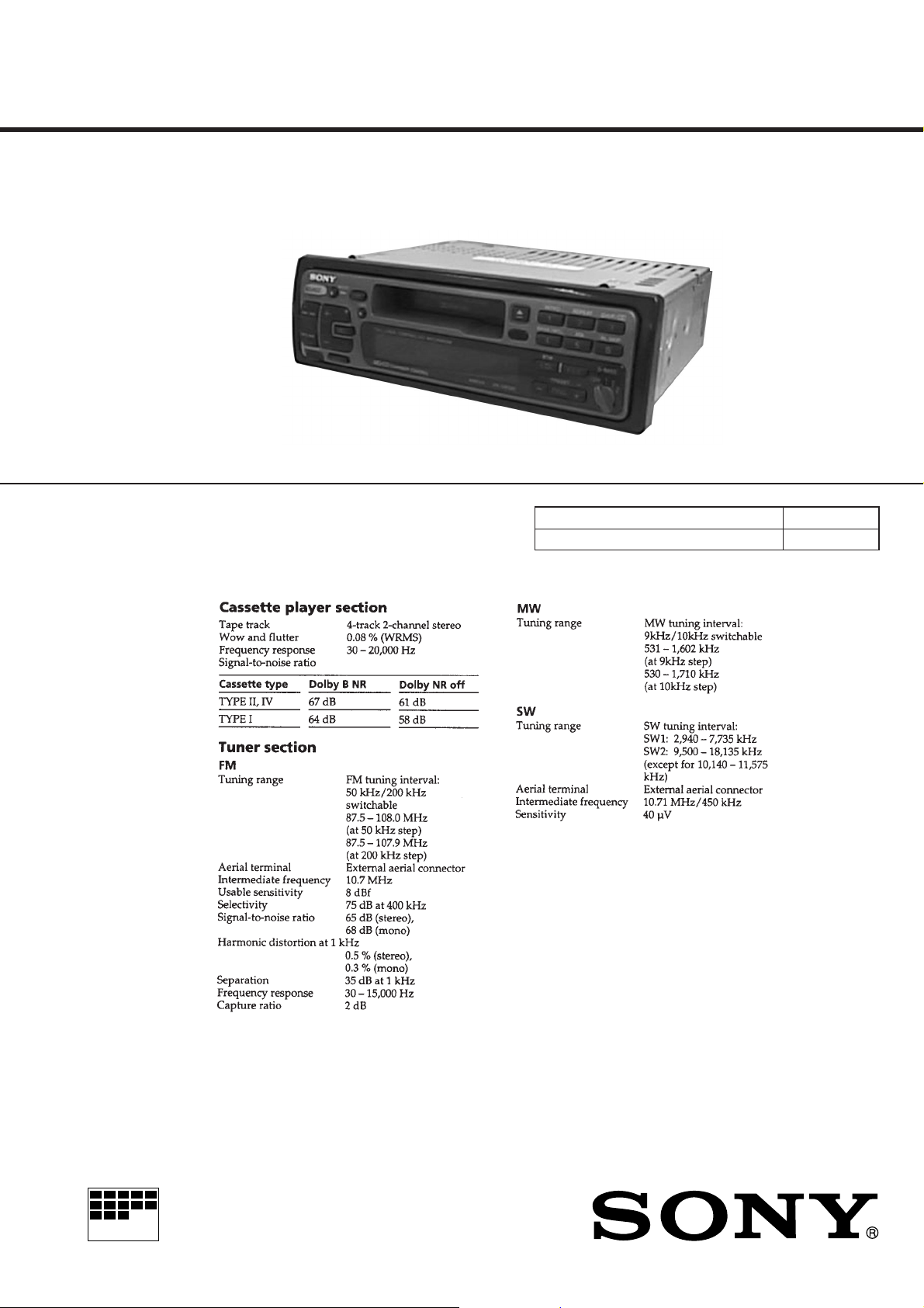
XR-C6100
SERVICE MANUAL
Dolby noise reduction manufactured under license
from Dolby Laboratories Licensing Corporation.
“DOLBY” and the double-D symbol a are trademarks of Dolby Laboratories Licensing Corporation.
SPECIFICATIONS
Saudi Arabia Model
Model Name Using Similar Mechanism NEW
Tape Transport Mechanism Type MG-25F-136
MICROFILM
– Continued on next page –
FM/MW/SW CASSETTE CAR STEREO
Page 2

SECTION 6
DIAGRAMS
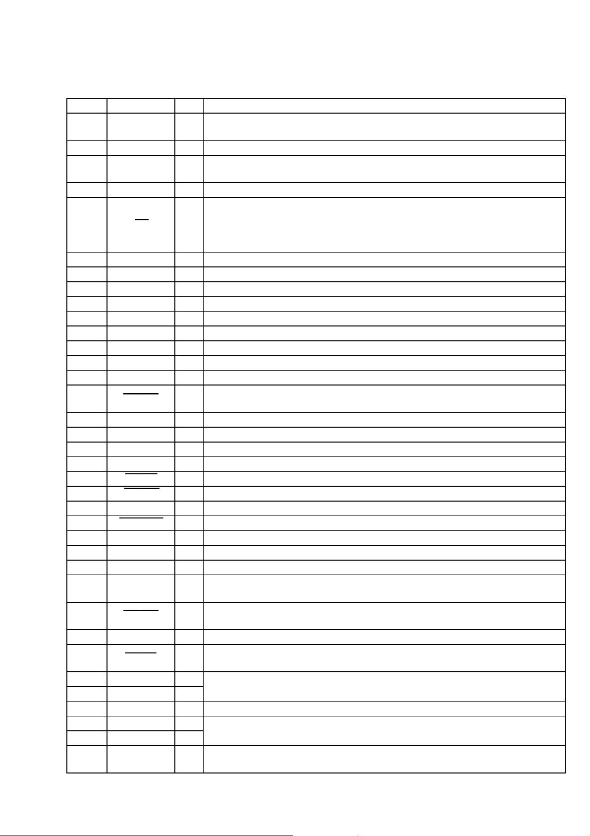
6-1. IC PIN FUNCTION DESCRIPTION
• MAIN BOARD IC501 µPD78058GC-F58-3B9 (SYSTEM CONTROLLER)
Pin No. Pin Name I/O Function
1 DSEL I
2 RC IN0 I Rotary remote commander shift key A/D input terminal
3 SD IN I
4 AVSS — Ground terminal (for A/D converter)
5 ST I/O
6 PLLCE O PLL serial chip enable output to the FM/AM PLL (IC1)
7 AVREF1 I Reference voltage (+5V) input terminal (for D/A converter)
8 PLLSI I PLL serial data input from the FM/AM PLL (IC1)
9 PLLSO O PLL serial data output to the FM/AM PLL (IC1)
10 PLLCKO O PLL serial data transfer clock signal output to the FM/AM PLL (IC1)
11 P-STIN I Polar stereo signal input terminal Not used (fixed at “H”)
12 LCDSO O Serial data output to the liquid crystal display driver (IC901)
13 LCDCKO O Serial data transfer clock signal output to the liquid crystal display driver (IC901)
14 LCDCE O Chip enable output to the liquid crystal display driver (IC901)
15 LCDINH O
16 UNISI I Serial data input from the bus interface (IC701) (for SONY bus)
17 UNISO O Serial data output to the bus interface (IC701) (for SONY bus)
18 UNICKI I Serial data reading clock signal input terminal (for SONY bus)
19 UNICKO O Serial data transfer clock signal output to the bus interface (IC701) (for SONY bus)
20 BUSON O Bus on/off control signal output to the bus interface (IC701) (for SONY bus) “L”: bus on
21 SYSRST O Reset signal output to the bus interface (IC701) (for SONY bus) “L”: reset
22 AMPON O Standby control signal output to the power amplifier (IC611) “L”: standby
23 AMP MUT O Muting control signal output to the power amplifier (IC611) “L”: muting on
24 TUNON O Tuner system power supply on/off control signal output to the BA3918 (IC671) “H”: tuner on
25 FM ON O FM system power supply on/off control signal output to the BA3918 (IC671) “H”: FM on
26 PW ON O Main system power supply on/off control signal output to the BA3918 (IC671) “H”: power on
27 COLOR I
28 AMSON O
29 REL I Reel table rotation detect signal input from the take-up and supply reel sensor
30 MTLIN I
31 POS3 I
32 POS2 I
33 GND — Ground terminal
34 POS0 I
35 POS1 I
36 LM LOD O
Destination setting terminal Frequency select switch (S502) input in this set
“L”: MW 9k step or FM 50k step, “H”: MW 10k step or FM 200k step
Station detector detect input from the FM/AM tuner unit (TU1)
Stop level for SEEK, BTM, etc. is determined SD is present at input of “H”
Input of FM stereo detection signal from FM/AM tuner unit (TU1), and output of forced
monaural control signal to FM/AM tuner unit (TU1) (Commonly used for stereo display input
and forced monaural output)
FM stereo detection at input of “L”, forced monaural at output of “L”
Blank indicate control signal output to the liquid crystal display driver (IC901)
“L”: no display
Input terminal to set whether the illumination color change function is present or not
“L”: illumination color change function is present (fixed at “L” in this set)
Tape auto music sensor control signal output to the CXA2510AQ (IC301)
“L” is output to lower the gain for audio level at FF/REW
Input terminal to set whether the auto metal function is present or not
“L”: auto metal function is present Not used this function in this set (fixed at “H”)
Tape position detect input from the tape operation switch on the mechanism block
Tape position detect input from the tape operation switch on the mechanism block
Loading/tape operation motor control signal output to the LB1638M (IC361)
(For the loading direction and forward side operation) *1
– 17 –
Page 3

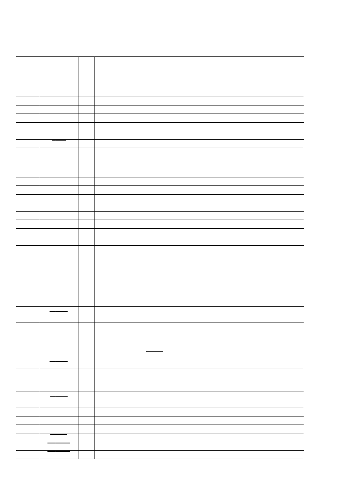
Pin No. Pin Name I/O Function
37 LM EJ O
38 N/R OUT O
39 P.ON O Polar stereo detection signal output terminal “H”: polar stereo Not used (open)
40 CM ON O Capstan/reel motor (M901) drive signal output terminal “H”: motor on
41 TAPEON O Tape system power supply on/off control signal output terminal “H”: tape on
42 COLSEL I Setting terminal for the illumination color “L”: amber, “H”: green (fixed at “H”)
43 RC IN1 I Rotary remote commander shift key A/D input terminal
44 TEST I Setting terminal for the test mode “L”: test mode (normally fixed at “H”)
45 ILL ON O
46 BEEP O Beep sound signal output terminal
47 MUT O Line muting control signal output terminal “H”: line muting on
48 VOLCE O Chip enable signal output to the electrical volume (IC161)
49 SUBCE O Chip enable signal output terminal Not used in this set (open)
50 VOLCKO O Serial data transfer clock signal output to the electrical volume (IC161)
51 SUBCKO O Serial data transfer clock signal output terminal Not used in this set (open)
52 VOLSO O Serial data output to the electrical volume (IC161)
53 TAPMUT O Tape muting on/off control signal output to the CXA2510AQ (IC301) “H”: tape muting on
54 DOLON I/O
Loading/tape operation motor control signal output to the LB1638M (IC361)
(For the eject direction and reverse side operation) *1
Forward/reverse direction control signal output to the CXA2510AQ (IC301)
“L: forward direction, “H”: reverse direction
Power supply on/off control signal output terminal at the illumination and liquid crystal display
driver (IC901) “H”: power on
At power select switch (S501) on mode: “H” output at the accessory on
At power select switch (S501) off mode: “H” output at the power on
Dolby control in/out terminal
At initial mode: valid/invalid selection input of dolby function (“L” input: valid)
At normal mode: dolby on/off control signal output to the CXA2510AQ (IC301)
“H”: dolby on
Dolby B/C selection control in/out terminal
55 DOLBC I/O
56 AMSIN I
57 MTLSEL I/O
58 AD ON O Power supply on/off control signal output for the A/D converter “L”: power on
59 RAMBU I
60 RESET I
61 SIRCS I Sircs signal input from the remote control receiver (IC902)
62 BU IN I Battery detect signal input terminal “H”: battery on
63 PW SEL I Power select switch (S501) input terminal “L”: off (halt mode), “H”: on (operation mode)
64 ACCIN I Accessory detect signal input terminal “L”: accessory on
65 NOSESW I Detects the removal of the attaching and removing type front panel block “L”: attaching
66 TELMUT I Telephone muting signal input terminal At input of “L”, the signal is attenuated by –20 dB
At initial mode: dolby B only/dolby B and C type selection input (“L” input: dolby B and C)
At normal mode: dolby type selection signal output “L”: dolby B, “H”: dolby C
Not used this function (fixed at “H”)
Whether a music is present or not from CXA2510AQ (IC301) is detected at auto music sensor
“L”: music is present, “H”: music is not present
METAL control in/out terminal
At initial mode: auto/manual mode selection input of METAL function “L”: manual mode
At manual mode: METAL on/off control signal output to the CXA2510AQ (IC301)
“H”: METAL on
At auto mode: input at MTLIN (pin #º)
Internal RAM reset detection signal input from the RN5VD23AA (IC651)
Input terminal to check that RAM data are not destroyed due to low voltage
This checking is made within 100 msec after reset
System reset signal input from the reset signal generator (IC652) and reset switch (S503)
“L” is input for several 100 msec after power on, then it changes to “H”
– 18 –
Page 4

Pin No. Pin Name I/O Function
67 KEYACK I
68 VDD — Power supply terminal (+5V)
69 X OUT O Main system clock output terminal (5 MHz)
70 X IN I Main system clock input terminal (5 MHz)
71 GND — Ground terminal
72 XT OUT O Sub system clock output terminal (32.768 kHz)
73 XT IN I Sub system clock input terminal (32.768 kHz)
74 AVDD — Power supply terminal (+5V) (for A/D converter)
75 AVREF0 I Reference voltage input terminal (+5V) (for A/D converter)
76 KEYIN0 I
77 KEYIN1 I
78 D-BASS I D-BASS switch (SW951) input (A/D input)
79 VSM I FM and AM signal meter voltage detection input from the FM/AM tuner unit (TU1)
80 KEYSEL I Setting terminal for the key (fixed at “L”)
Input of acknowledge signal for the key entry Acknowledge signal is input to accept function
and eject keys in the power off status On at input of “H”
Key input terminal (A/D input)
OFF, SOURCE, MODE *, SEEK AMS + + ), SEEK AMS = 0 –, VOLUME –,
SEL, VOLUME +, DSPL, ATT keys input (LSW901 to LSW910)
Key input terminal (A/D input)
6, INTRO 1, REPEAT 2, SHUF/a 3, BL SKIP 6, ATA 5, BANK/MTL 4, BTM LCL, FILE,
PRESET DISC +/– keys input (LSW921 to LSW931)
*1 loading/tape operation motor control
MODE
TERMINAL
LM LOD (pin #§) “L” “H” “L” “H”
LM EJ (pin #¶) “L” “L” “H” “H”
STOP
LOADING/
FORWARD
EJECT/
REVERSE
BRAKE
– 19 –
Page 5

XR-C6100
6-4. SCHEMATIC DIAGRAM – MAIN Section (1/2) – • See page 31 and 32 for IC Block Diagrams.
– 23 –
– 24 –
Page 6

6-5. SCHEMATIC DIAGRAM – MAIN Section (2/2) – • See page 32 for IC Block Diagramas.
XR-C6100
• Wavef orms
1 IC1 1 (XO)
4.2 Vp-p
7.2 MHz
2 IC501 ^ª (XOUT)
5 MHz
3 IC501 &™ (XT_OUT)
4.6 Vp-p
5 Vp-p
– 25 –
32.768 kHz
– 26 –
Page 7

6-7. SCHEMATIC DIAGRAM – PANEL Section –
XR-C6100
– 29 –
– 30 –
Page 8

• IC Block Diagrams
– MAIN BOARD –
IC1 BU2624F-E2
1
XOUT
2
XIN
3
CE
4
CK
5
DA
6
CD
7
P0
8
P1
9
P3
10
P4
I/O
CONTROL
REFERENCE
DIVIDER
SHIFT
REGISTER
LATCH
20BIT COUNT
MAIN
COUNT
IF COUNT
CONTROL
PHASE
DETECT
PRESCALLER
IC301 CXA2510AQ-T4
20
VSS
19
PD1
18
VDD
PBFB1
PBRIN1
17
FMIN
16
AMIN
15
P2
14
IF1
13
IF2
12
SD
11
PD2
PBREF1
PBFIN1
VCT
PBGND
PBFIN2
PBREF2
PBRIN2
PBFB2
PBEQ1
PBOUT1
120µ/
70µ
+
–
31
32
1
PBEQ2
VCT
F2
F1
–
+
120µ/
70µ
2
PBOUT2
33
34
35
36
37
38
39
40
AUXIN1
TAPEIN1
GND
T2
LPF
MSLPF
NR BIAS
TAPE/AUX
TAPE EQ
FWD/RVS
VCC
F3
+
LINEOUT2
X1
+
X1
T1
345 6 7 8 9 10
VCC
AUXIN2
TAPEIN2
LINEOUT1
DIREF
2425
+
–
+
–
–
OFF/B
NR
NC
TCH2
NR
OFF/B
PLAY
TCH1
NC
MSSW
2122232627282930
MS
MODE
NR
MODE
DETECT
MS ON/
OFF
20
19
18
17
16
15
14
13
12
11
MSMODE
DRSW
TAPESW
INSW
NRSW
NC
MSOUT
DGND
MSTC
FF
IC161 LC75373ED
LVRIN
+
–
34
LSELO
35
L4
L3
36
L2
VDD
RSELO
37
L1
38
39
R1
40
41
R2
R3
42
R4
43
44
+
–
–
+
–
+
LCOM
IC361 LB1638M
10
1
GND
SHIFT
REGISTER
2324252627282930313233
LSOUT
CONTROL
2
IN1
VCC
22
LFIN
+
–
+
–
–
+
–
+
LFOUT
21
LROUT
20
19
VREF
18
CE
17
DI
16
CL
15
VSS
14
RROUT
RFOUT
13
12
RFIN
3
4
IN2
5 6
GND
CONTROL LOGIC
IC671 BA3918-V2
REGULATOR
LS3
LS1
LSIN
LT3
LT2
LT1
+
–
+
–
+
–
–
+
LTOUT
–
+
DECODER LATCH
+
–
LS2
–
+
–
+
+
–
+
–
N.C.
9
OUT1
VS
8
7
OUT2
N.C.
IC611 TDA7384
DRIVER
5
3 4
1
2
TAB
GND
OUT2–
OUT2+
STNBY
6
VCC
DRIVER
7 8
OUT1–
GND
10 12
9
OUT1+
SVR
11
14
16
S-GND
IN4
17
15
IN3
AC-GND
IN1
13
IN2
IC701 BA8270F-E2
BUS ON
RST
BATT
DRIVER
OUT3+
1
2
3
GND
1918
OUT3–
20
VCC
BUS ON
SWITCH
RESET
SWITCH
BATTERY
SWITCH
DRIVER
21
OUT4+
2322
MUTE
24
OUT4–
GND
14
13
12
11
10
25
N.C.
VCC
RST
BUS ON
CLK IN
BU IN
1
RVRIN
2 345 6 7 8 9 10
RT1
RT2
RCOM
RT3
RSIN
RTOUT
RS1
RS2
RS3
– 31 –
11
RSOUT
OVER VOLTAGE
PROTECT
–
+
2 3
4
1
NC
STB
MODE2
MODE1
5 6 7 8 9 10 1211
VCC
AMP
ANT
COM
VDD
–
+
AM
–
+
FM
–
+
GND
4
CLK
5
VREF
6
DATA
GND
7 8
DATA IN
9
DATA OUT
– 32 –
 Loading...