

Page 1
XR-C6090R/C6100R
SERVICE MANUAL
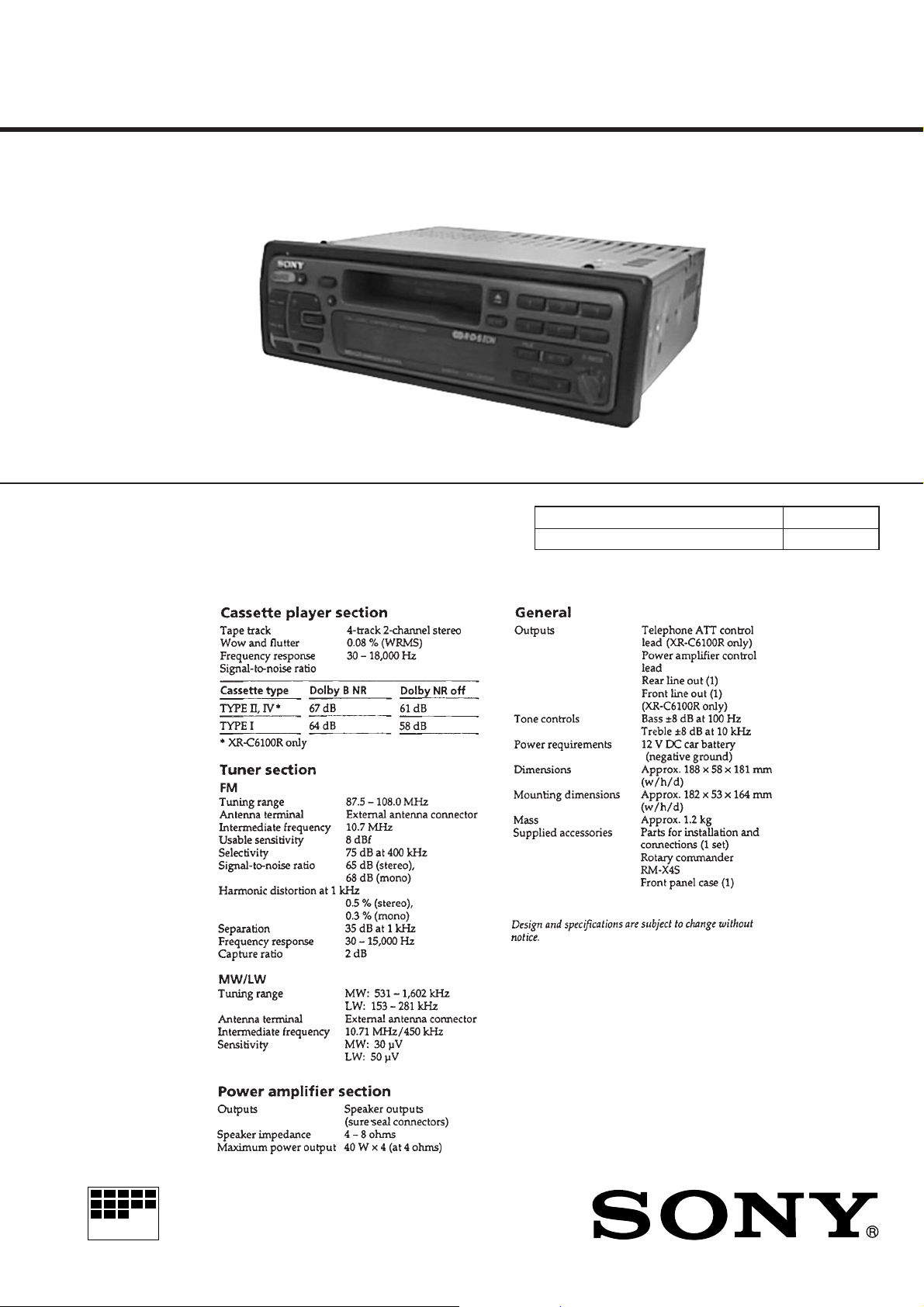
Photo: XR-C6100R
Dolby noise reduction manufactured under license
from Dolby Laboratories Licensing Corporation.
”DOLBY“ and the double-D symbol a are trademarks
of Dolby Laboratories Licensing Corporation.
SPECIFICA TIONS
AEP Model
UK Model
Model Name Using Similar Mechanism XR-5800R
Tape T ransport Mechanism T ype MG-25G-136
MICROFILM
FM/MW/LW CASSET TE CAR STEREO
Page 2

TABLE OF CONTENTS
1. GENERAL
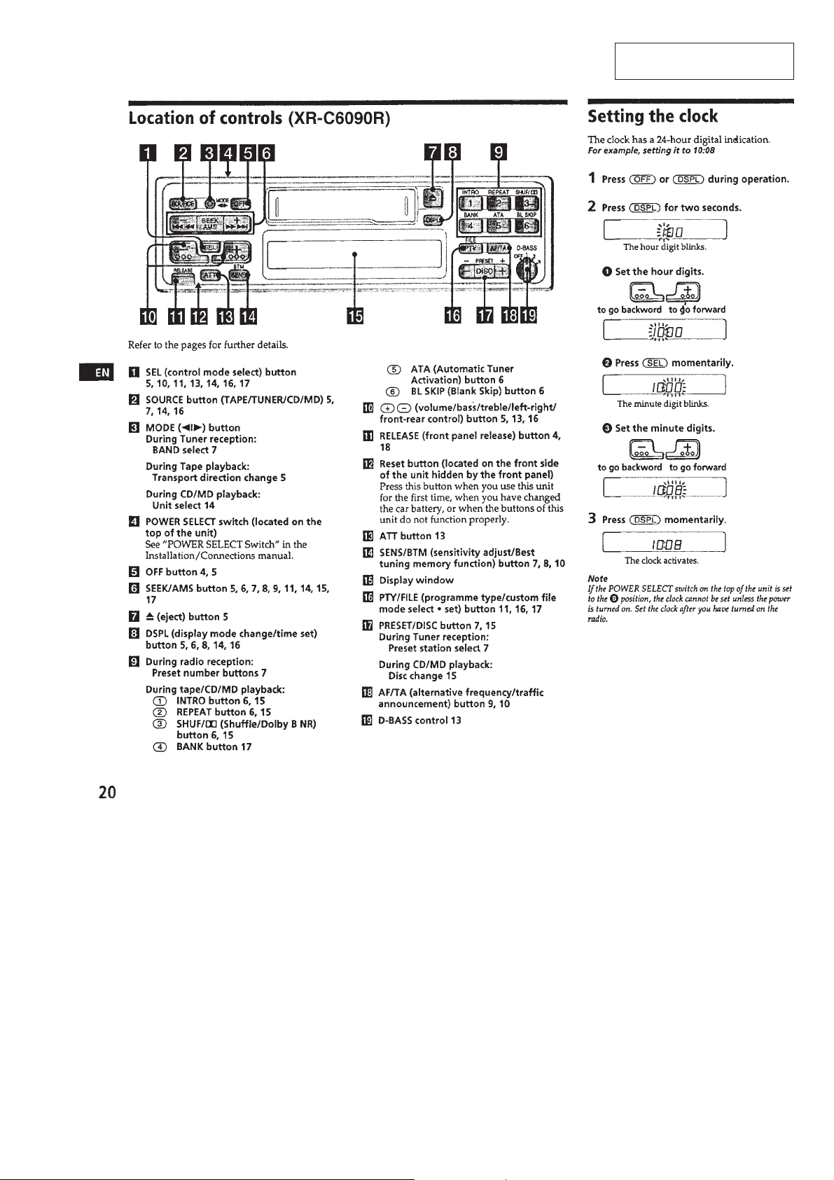
Location of Controls (XR-C6090R) ............................... 3
Setting the Clock ............................................................. 3
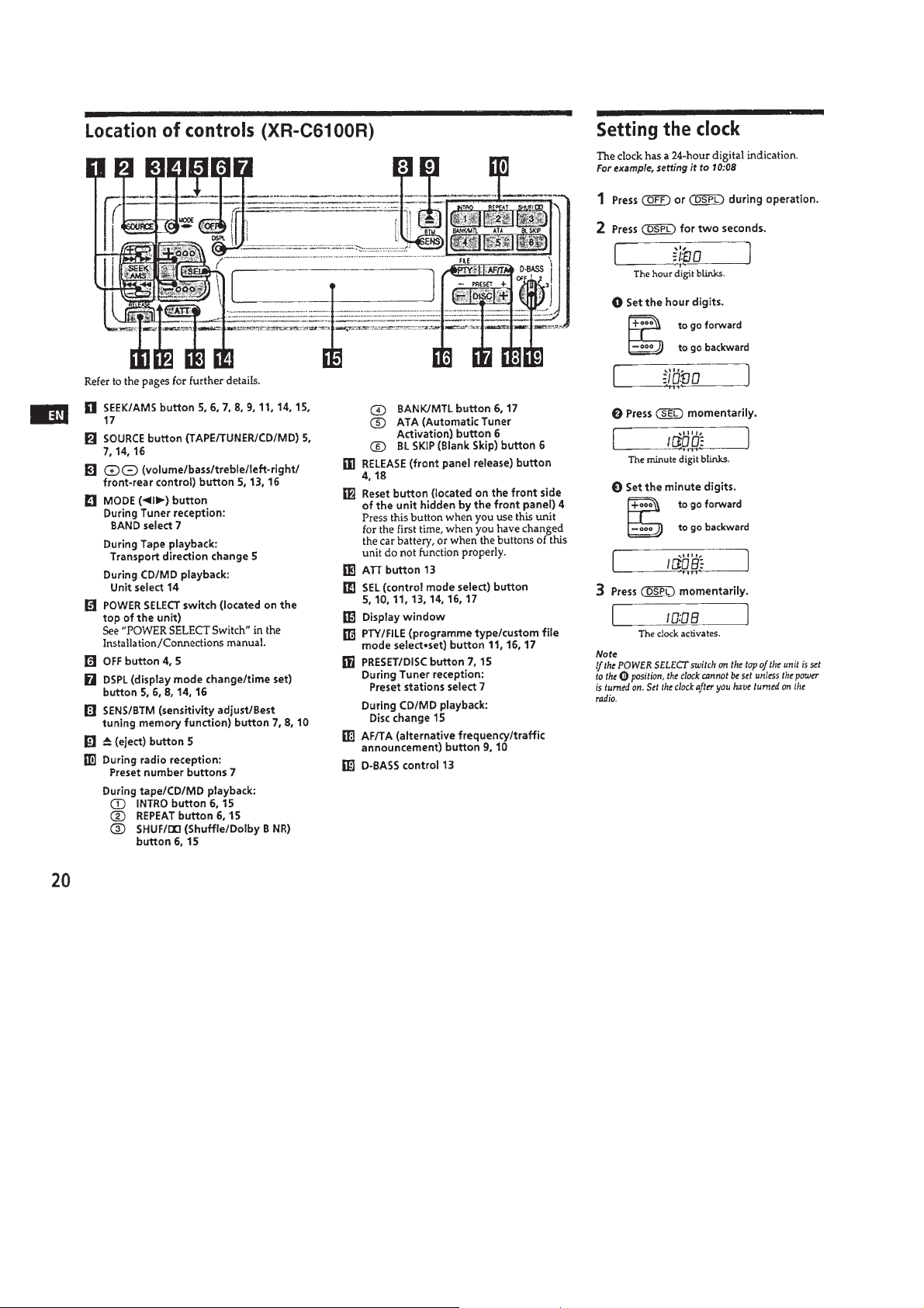
Location of Controls (XR-C6100R) ............................... 4
Setting the Clock ............................................................. 4
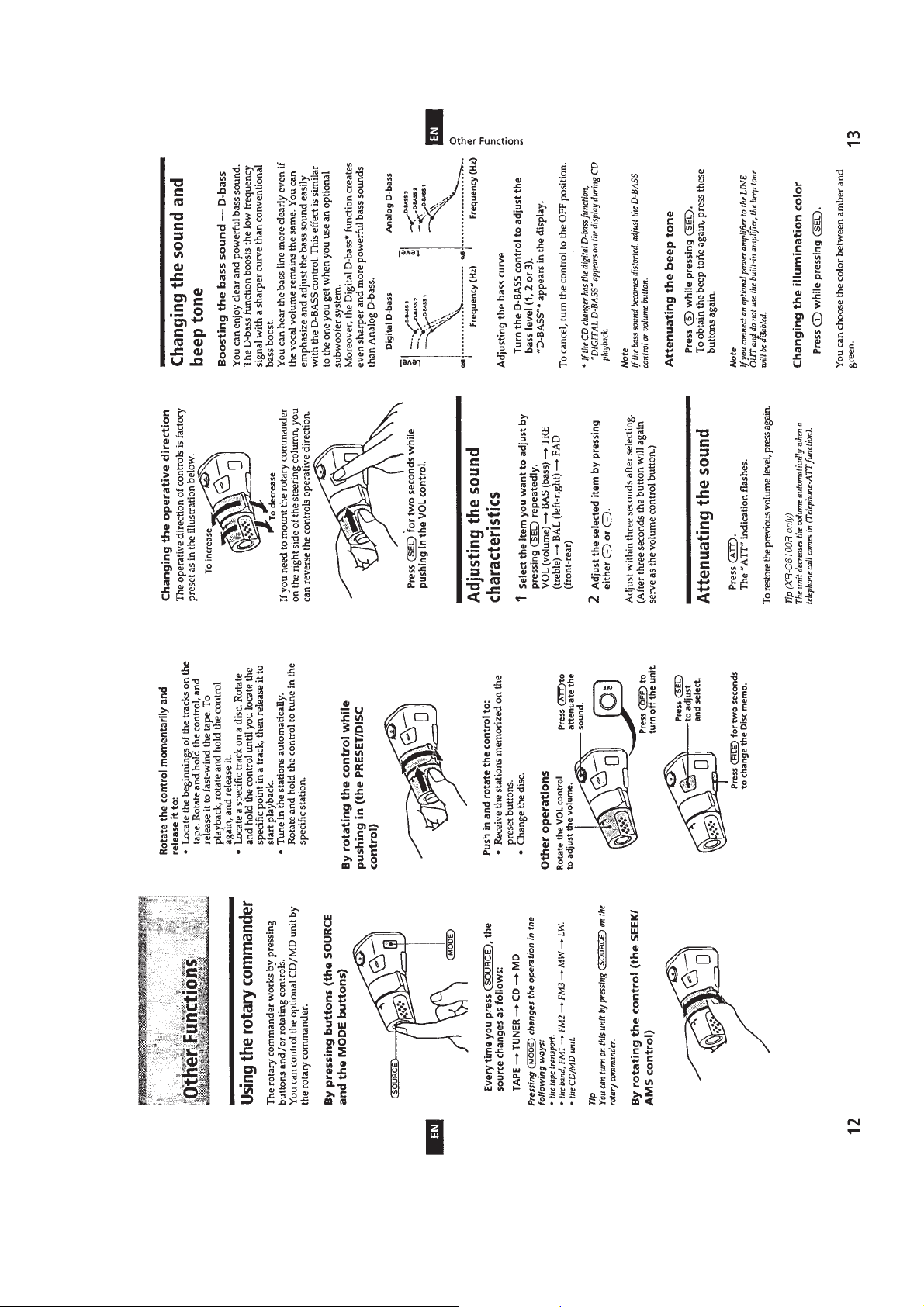
Using the Rotary Commander ........................................ 5
Adjusting the Sound Characteristics .............................. 5
Attenuating the Sound .................................................... 5
Changing the Sound and Beep Tone............................... 5
Installation....................................................................... 6
Connections ..................................................................... 7
2. DISASSEMBLY ......................................................... 10
3. ASSEMBLY OF MECHANISM DECK........... 12
4. MECHANICAL ADJUSTMENTS....................... 15
5. ELECTRICAL ADJUSTMENTS
Test Mode........................................................................ 15
Tape Deck Section .......................................................... 15
Tuner Section .................................................................. 16
6. DIAGRAMS
6-1. Printed Wiring Boards – MAIN Section – .................... 20
6-2. Schematic Diagram – MAIN Section –.......................... 23
6-3. Printed Wiring Board
– PANEL Section – (XR-C6090R) ................................ 28
6-4. Schematic Diagram
– PANEL Section – (XR-C6090R) ................................ 30
6-5. Printed Wiring Board
– PANEL Section – (XR-C6100R) ................................ 33
6-6. Schematic Diagram
– PANEL Section – (XR-C6100R) ................................ 35
6-7. IC Pin Function Description ........................................... 41
Flexible Circuit Board Repairing
• Keep the temperature of the soldering iron around 270 ˚C during repairing.
• Do not touch the soldering iron on the same conductor of the
circuit board (within 3 times).
• Be careful not to apply force on the conductor when soldering
or unsoldering.
Notes on chip component replacement
• Never reuse a disconnected chip component.
• Notice that the minus side of a tantalum capacitor may be damaged by heat.
7. EXPLODED VIEWS ................................................ 44
8. ELECTRICAL PARTS LIST ............................... 48
– 2 –
Page 3
SECTION 1
GENERAL
This section is extracted from
instruction manual.
– 3 –
Page 4
– 4 –
Page 5
– 5 –
Page 6
– 6 –
Page 7
– 7 –
Page 8
– 8 –
Page 9
– 9 –
Page 10
SECTION 2
DISASSEMBLY
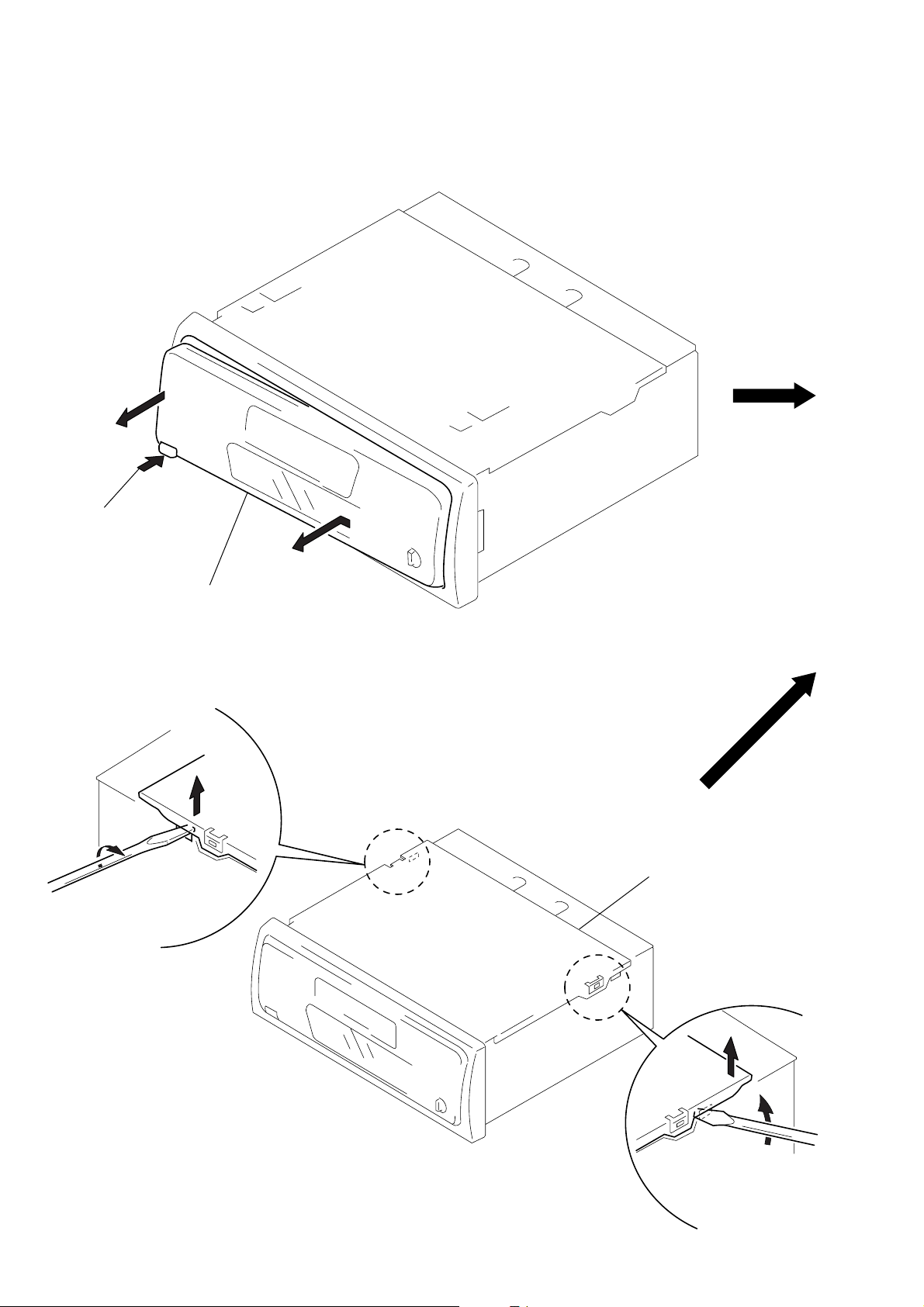
Note: Follow the disassembly procedure in the numerical order given.
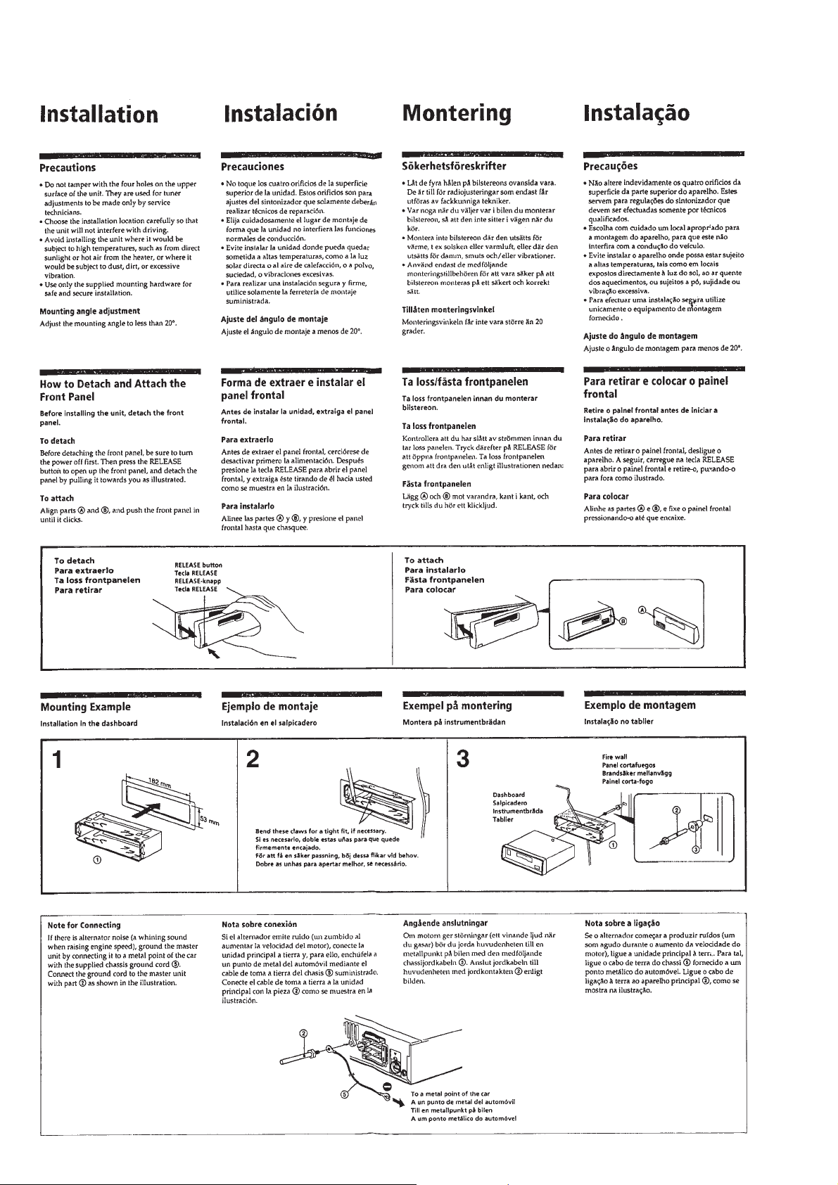
FRONT PANEL ASS’Y
1
Push the button
(release).
2
Remove the front panel ass’y
to the direction of the arrow
COVER ASS’Y
1
2
A
A
.
3
cover ass’y
– 10 –
2
1
Page 11
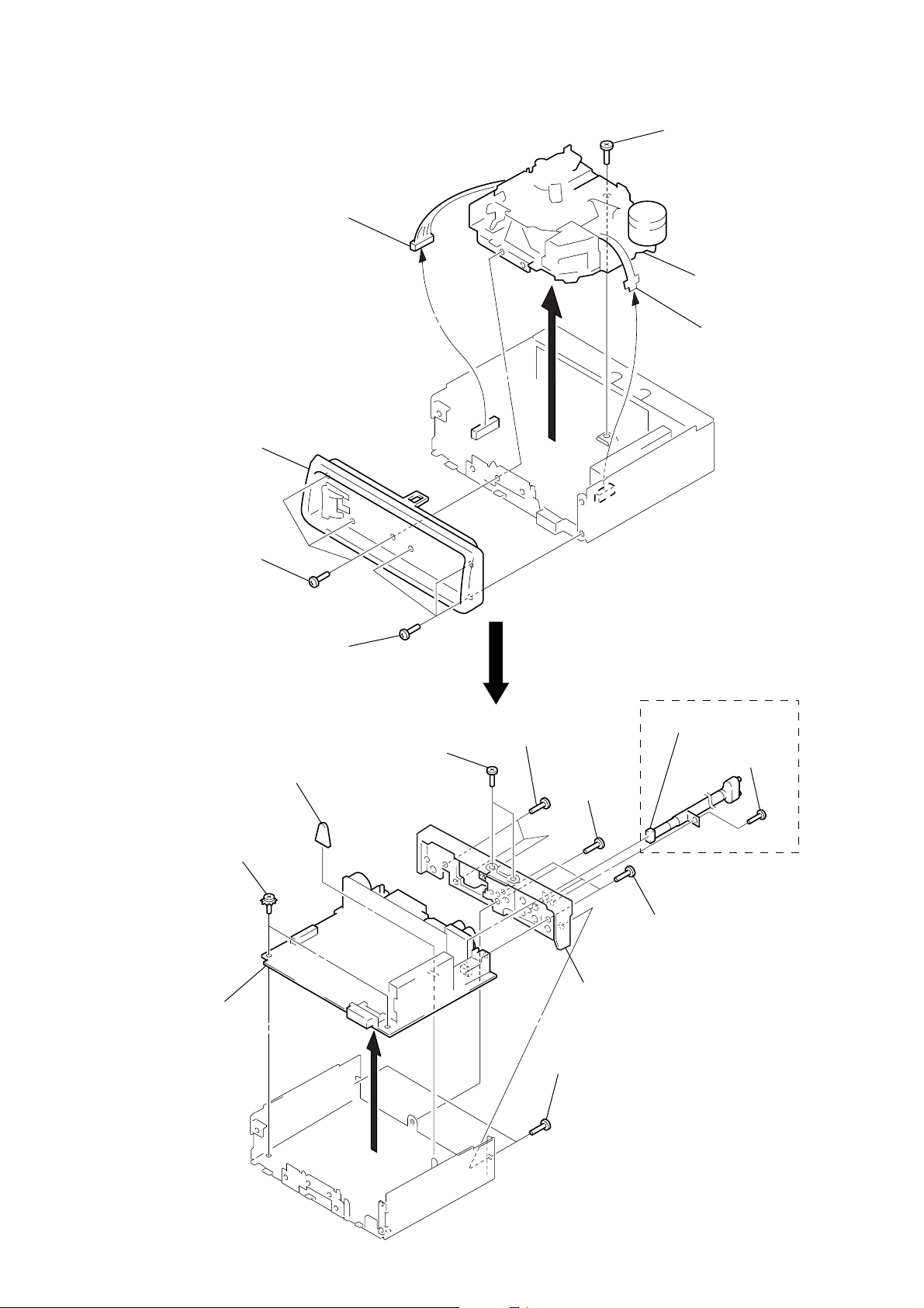
SUB PANEL, MECHANISM DECK (MG-25G-136)
e
3
connector
(CN352)
2
sub panel
1
three screws
(PTT2.6 × 8)
5
screw
(PTT2.6 × 6)
6
4
mechanism deck
(MG-25G-136)
flexible flat cabl
(CN351)
1
three screws
(PTT2.6 × 8)
MAIN BOARD, HEAT SINK
4
rabber cap (25)
5
two ground point
screws
6
main board
7
two screws
(PTT2.6
×
14)
8
three screws
(PTT2.6
×
10)
3
screw
(PTT2.6
3
two screws
(PTT2.6
9
heat sink
×
8)
8
×
8)
2
cord (with connector)
(line out front) (CN151)
1
screw
(PTT2.6
XR-C6100R
three screws
(PTT2.6
×
10)
×
8)
– 11 –
Page 12
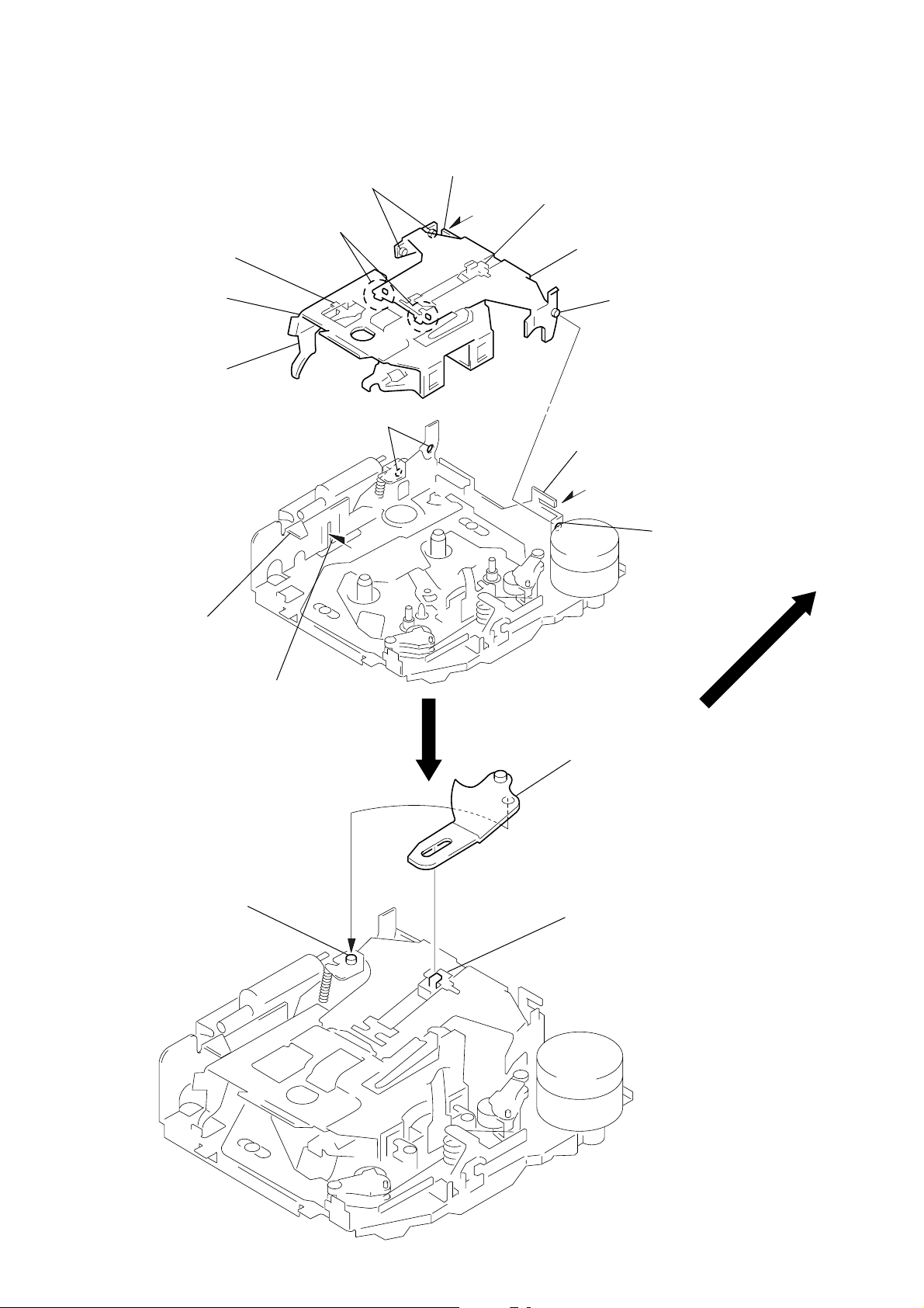
SECTION 3
ASSEMBLY OF MECHANISM DECK
Note: Follow the assembly procedure in the numerical order given.
HOUSING
4
Fit claw on B part.
3
Put the housing
under A part.
housing
5
Fit projection on C part.
2
Install the hanger onto
two claws of the housing.
C
part
7
Holder the hanger by bending the claw.
1
Install the catch to the hanger.
hanger
6
Fit projection on D part.
8
Hold the hanger by
bending the claw.
D
part
ARM (SUCTION)
A
part
projection
B
part
2
Move the arm (suction) in the arrow
direction and fit on projection.
1
Fit the arm (suction) on the shaft.
– 12 –
Page 13
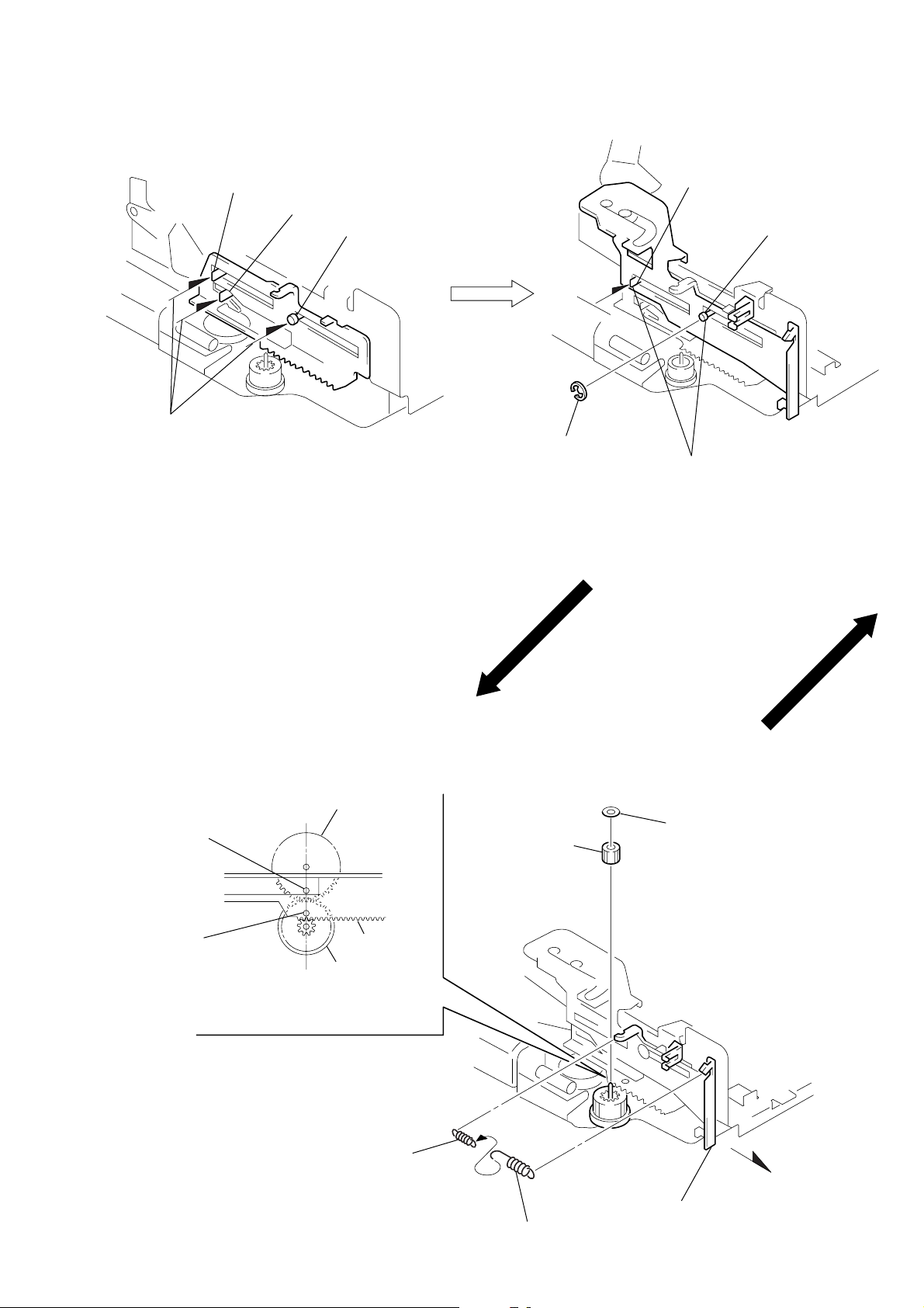
LEVER (LDG-A) / (LDG-B)
shaft
A
shaft
1
Fit the lever (LDG-A) on
shafts A – C and install it.
B
shaft
C
3
type-E stop ring 2.0
shaft
A
Fit the lever (LDG-B) on
2
shafts
install it.
A
and B and
shaft
B
GEAR (LDG-FT)
hole
hole
gear (LDG-D)
lever (LDG-A)
gear (LDG-FB)
4
Align hole in the gear (LDG-D)
with hole the lever (LDG-A).
2
tension spring (LD-2)
5
gear (LDG-FT)
1
6
polyethylene washer
2
tension spring (LD-1)
– 13 –
3
Move the lever (LDG-B)
in the arrow direction.
Page 14

GUIDE (C)
2
guide (C)
1
three claws
– 14 –
Page 15

SECTION 4
MECHANICAL ADJUSTMENTS
SECTION 5
ELECTRICAL ADJUSTMENTS
1. Clean the following parts with a denatured-alcohol-moistened
swab:
playback head pinch roller
rubber belt capstan
idlers
2. Demagnetize the playback head with a head demagnetizer.
3. Do not use a magnetized screwdriver for the adjustments.
4. After the adjustments, apply suitable locking compound to the
parts adjusted.
5. The adjustments should be performed with the power supply
voltage unless otherwise noted.
• T orque Measurement
Mode Torque Meter Meter Reading
Forward CQ-102C
Forward
Back Tension (0.01 - 0.06 oz•inch)
Reverse CQ-102RC
Reverse
Back Tension (0.01 - 0.06 oz•inch)
FF, REW CQ-201B
CQ-102C
CQ-102RC
30 - 65 g•cm
(0.42 - 0.90 oz•inch)
0.5 - 4.5g•cm
30 - 65 g•cm
(0.42 - 0.90 oz•inch)
0.5 - 4.5g•cm
60 - 200 g•cm
(0.83 - 2.78 oz•inch)
• T ape Tension Measurement
Mode Tension Meter Meter Reading
Forward CQ-403A
Reverse CQ-403R
more than 90 g
(more than 3.18 oz)
more than 90 g
(more than 3.18 oz)
TEST MODE
This set have the test mode function. In the test mode, FM Auto
Scan/Stop Level and AM (MW) Auto Scan/Stop Lev el adjustments
can be performed easier than it in ordinary procedure.
<Set the Test Mode>
1. Set the “power select” switch (S801) is “A” position.
2. Turn ON the regulated power supply. (All LEDs on the set
lights up, and the clock is displayed.)
Note: Press the [OFF] button, if the clock is not displayed.
3. Push the preset [4] button.
4. Push the preset [5] button.
5. Press the preset [1] button for more than two seconds.
6. Then the display indicates all lights, the test mode is set.
<Release the Test mode>
1. Push the [OFF] button.
2. Return the “power select” switch (S801) to initially set position.
See the adjustment location from on page 19 for the
adjustment.
TAPE DECK SECTION
0 dB=0.775 V
Tape Speed Adjustment
Setting:
speed checker
or
test tape
WS-48A
(3 kHz, 0 dB)
frequency counter
4
Ω
set
speaker out terminal
+–
Procedure:
1. Put the set into the FWD PB mode.
2. Adjust adjustment resistor for inside capstan motor so that the
reading on the speed checker or frequency counter becomes in
specification.
Specification: Constant speed
Speed checker Frequency counter
–1.5 to +2.5% 2,955 to 3,075 Hz
Adjustment Location: See page 19.
– 15 –
Page 16

Dolby Level Adjustment
r
Setting:
Preset [3] (DOLBY) button : NR OFF
SEL (BAS) button : Center
SEL (TRE) button : Center
SEL (BAL) button : Center
SEL (FAD) button : Center
SEL (VOL) button : Maximum
D-BASS control : OFF
test tape
P-4-D400
(400Hz, 0dB)
MAIN board
TP (DOLBY L)/
TP (DOLBY R)
level mete
TUNER SECTION
0 dB=1 µV
Cautions during repair
When the tuner unit is defective, replace it by a new one because its internal block is difficult to repair.
Note:
Adjust the tuner section in the sequence shown below.
1. FM Auto Scan/Stop Level Adjustment
2. FM Noise Focus Adjustment
3. FM Stereo Separation Adjustment
4. FM Signal Meter Adjustment
5. AM (MW) Auto Scan/Stop Level Adjustment
set
MAIN board
TP (GND)
+
–
Procedure:
1. Put the set into the FWD PB mode.
2. Adjust RV401 (L-CH) and RV301 (R-CH) so that the level
meter reading is –6±1 dBs (0.35 to 0.43 V).
Adjustment Location: See page 19.
FM Auto Scan/Stop Level Adjustment
Setting:
[SOURCE] button: FM
FM RF signal
generator
Carrier frequency : 98.0 MHz
Output level : 22 dB (12.6
Mode : mono
Modulation : 1 kHz, 22.5 kHz deviation (30%)
Procedure:
1. Set to the test mode. (See page 15.)
2. Push the
[SOURCE] button and set to FM.
FM
3. Adjust with the volume R V2 on TU1 so that the “FM” indication turns to “FM0” indication on the display window.
But, in case of already indicated “FM0”, turn the RV2 so that
put out light “0” indication and adjustment.
antenna jack (J1)
0.01 µF
Display
REG
set
µ
V)
INTRO
Display
REG
INTRO
Adjustment Location: See page 19.
– 16 –
Page 17

FM Noise Focus Adjustment
INTRO
FM
FM
INTRO
REG
Setting:
[SOURCE] button: FM
FM Signal Meter Adjustment
Setting:
[SOURCE] button: FM
FM RF signal
generator
Carrier frequency : 98.00 MHz
Output level : 60 dB (1 mV)
Mode : stereo
Modulation : 1 kHz, 75 kHz deviation (100%)
antenna jack (J1)
0.01 µF
4
set
speaker out terminal
level meter
Ω
+
–
Procedure:
1. Tuner the 98.00 MHz.
2. The then output level is supposing that (A) dB.
3. Adjust with the volume R V3 on TU1 so that the output le vel is
(A) –32 ± 2 dB then signal generator input set to –20 dB.
Adjustment Location: See page 19.
FM Stereo Separation Adjustment
Setting:
[SOURCE] button: FM
FM RF signal
generator
antenna jack (J1)
0.01 µF
4
set
level meter
Ω
+
–
FM RF signal
generator
Carrier frequency : 98.00 MHz
Output level : 35 dB (56.2
Mode : mono
Modulation : no modulation
antenna jack (J1)
0.01 µF
set
µ
V)
Procedure:
1. Set to the test mode. (See page 15.)
2. Push the
[SOURCE] button and set to FM.
Display
3. Push the [6] button.
4. Adjust RV1 so that the display indication is “160”.
Display
Specification: Display indication: 158 to 162
Adjustment Location: See page 19.
Carrier frequency : 98.0 MHz
Output level : 70 dB (3.2 mV)
Mode : stereo
Modulation : main: 1 kHz, 20 kHz deviation (26.7%)
sub: 1 kHz, 20 kHz deviation (26.7%)
: 19 kHz pilot: 7.5 kHz deviation (10%)
speaker out terminal
Procedure:
FM Stereo
signal generator
output channel
L-CH L-CH A
R-CH L-CH Adjust RV4 on TU1
R-CH R-CH C
L-CH R-CH Adjust RV4 on TU1
Level meter Level meter
connection reading (dB)
B
for minimum reading.
D
for minimum reading.
L-CH Stereo separation: A-B
R-CH Stereo separation: C-D
The separations of both channels should be equal.
Specification: Separation more than 30 dB
Adjustment Location: See page 19.
– 17 –
Page 18

AM (MW) Auto Scan/Stop Level Adjustment
µ
Make this adjustment after “FM Auto Scan/Stop Level Adjustment”.
Setting:
[SOURCE] button: MW
30
Ω
15 pF
65 pF
AM RF signal
generator
AM dummy antenna
(50 Ω)
set
Carrier frequency : 999 kHz
30% amplitude
modulation by
1 kHz signal
Output level : 33 dB (44.7
Procedure:
1. Set to the test mode. (See page 15.)
2. Push the
3. Push the
[SOURCE] button and set to FM.
[MODE] button and set to MW.
Display
MW
antenna jack (J1)
V)
INTRO
999 @
4. Adjust with the volume RV1 on TU1 so that the “MW” indication turns to “MW0” indication on the display window.
But, in case of already indicated “MW0”, turn the R V1 so that
put out light “0” indication and adjustment.
Display
INTRO
999
Adjustment Location: See page 19.
– 18 –
Page 19

Adjustment Location:
– SET UPPER VIEW –
Tape Speed Adjustment
TU1
RV1 AM (MW) Auto Scan/Stop Level Adjustment
RV2 FM Auto Scan/Stop Level Adjustment
RV3 FM Noise Focus Adjustment
RV4 FM Stereo Separation Adjustment
RV301
(R-CH)
– MAIN BOARD –
RV401
(L-CH)
Dolby Level
Adjustment
J1
antenna jack
TU1
(GND)
RV1 FM Signal Meter Adjustment
TP
(DOLBY R)
TP (DOLBY L)
IC351
TP
– 19 –
Page 20

Page 21

Page 22

Page 23

Page 24

• IC Block Diagrams – MAIN Section –
IC1 TB2114F (EL)
VCC
RF
A-GND
XTIN
24 23 22
RIPPLE
FILTER
SEEK/RECP
AM CP OUT
21
20 19 18
+
–
VCC
VT
+
–
4BIT
SWALLOW
COUNTER
FM CP OUT
SEEK/RECP
MODULAS
PRESCALER
17 16
PSC
2
D-GND
AM IN
AM/FM IF
VDD
FM IN
14
15
13
VDD
AMPAMPAMP
REF
PHASE
COMPARATOR
OSC IN
OR
X'TAL OSC
1
XTOUT
REFERENCE
COUNTER
ON/OFF
BUFFER
2
SC OUT
18BIT
18BIT
BUS INTERFACE
3
4
CE
DIN
IC3 TDA7330BD-013TR
POR
20
TM
19 18 17 16 15 14 13 12
2nd ORDER
ANTIALIAS
FILTER
FSEL
8th ORDER
SC-BANDPASS
FILTER
VCC
12BIT
SIG
PROGRAMABLE
COUNTER
40BIT
SHIFT
22BIT
RESISTER
N
I/O PORTS
DATA
6
5
CK
DOUT
T7
7 8 9 10
SR
+
–
TEST LOGIC
I/O-1
VCC
OUT PORTS
I/O-2
11
OUT-1
ARI
COSTAS
LOOP
PLL
57kHz
IF COUNTER
12
OUT-2
OUT-3
OUAL
20BIT
PHASE
DECODER
RECOVERY
1.4675kHz
CLOCK
PLL
RODA
DIFF
DECODER
ROCL
ON/OFF
OSCILLATOR
fx DIVIDER
T57
11
1
MPXIN
2
VREF
CMP
4
FILOUT
5
GND
T1
T3
T4
10986 73
OSCOUT
OSCIN
– 37 –
Page 25

IC151 LC75373ED
LSELO
VDD
RSELO
SHIFT
REGISTER
2324252627282930313233
11
LSOUT
CONTROL
RSOUT
22
LFIN
+
–
+
–
–
+
–
+
LFOUT
21
LROUT
20
19
VREF
18
CE
17
DI
16
CL
15
VSS
14
RROUT
RFOUT
13
12
RFIN
LS3
LS1
LSIN
LT3
LT2
LVRIN
34
35
L4
L3
36
L2
37
L1
38
39
R1
40
41
R2
R3
42
R4
43
44
1
RVRIN
LCOM
+
–
+
–
–
+
–
+
2 345 6 7 8 9 10
RCOM
LT1
+
–
+
–
+
–
–
+
RT1
RT2
RT3
LTOUT
–
+
DECODER LATCH
+
–
RS1
RSIN
RTOUT
LS2
–
+
–
+
+
–
+
–
RS2
RS3
IC351 CXA2510AQ-T4
PBEQ1
PBOUT1
GND
120µ/
70µ
+
–
PBFB1
31
32
PBRIN1
1
PBEQ2
VCT
F2
F1
–
+
120µ/
70µ
345 6 7 8 9 10
2
VCC
PBOUT2
PBREF1
PBFIN1
VCT
PBGND
PBFIN2
PBREF2
PBRIN2
PBFB2
33
34
35
36
37
38
39
40
TAPEIN1
X1
+
X1
TAPEIN2
AUXIN1
T1
AUXIN2
DIREF
2425
T2
LPF
MSLPF
NR BIAS
TAPE/AUX
TAPE EQ
FWD/RVS
VCC
+
–
F3
–
+
LINEOUT2
+
OFF/B
NR
–
TCH2
2122232627282930
NR
OFF/B
MS
MODE
NR
MODE
DETECT
NC
PLAY
MS ON/
OFF
20
19
18
17
16
15
14
13
12
11
MSMODE
DRSW
TAPESW
INSW
NRSW
NC
MSOUT
DGND
MSTC
FF
MSSW
NC
TCH1
LINEOUT1
– 38 –
Page 26

IC360 MM1322XFBE
1
GND
2
IN2
3
VCC
CONTROL CIRCUIT
4
IN1
IC601 BA3918-V2
REGULATOR
8
OUT2
7
VS
6
OUT1
5
GND
–
+
2 3
4
1
NC
STB
MODE2
MODE1
IC701 BA8270F-E2
BUS ON
1
2
RST
BATT
3
4
CLK
5
VREF
6
DATA
GND
7 8
BUS ON
SWITCH
RESET
SWITCH
BATTERY
SWITCH
OVER VOLTAGE
PROTECT
–
+
5 6 7 8 9 10 1211
VDD
AMP
14
13
12
11
10
9
VCC
ANT
VCC
RST
BUS ON
CLK IN
BU IN
DATA IN
DATA OUT
COM
AM
–
+
–
+
FM
GND
– 39 –
Page 27

• Waveforms – MAIN Section –
1 IC1 1 XO
200 ns
3 IC501 9 X OUT
125 ns
42 mVp-p
3.9 Vp-p
2 IC3 9 XO
5.1 Vp-p
230 ns
4 IC501 !™ XT OUT
5 Vp-p
30.6 µs
– 40 –
Page 28

6-7. IC PIN FUNCTION DESCRIPTION
• MAIN BOARD IC501 MN1886426SA (SYSTEM CONTROLLER)
Pin No. Pin Name I/O Function
1 TUNMUT O FM audio signal muting control output terminal “H”: muting on
2 AMPON O Standby control signal output to the power amplifier (IC801) “L”: standby
Power supply on/off control signal output terminal at the illumination and liquid crystal display
3 ILLON O
4 PW ON O Main system power supply on/off control signal output to the BA3918 (IC601) “H”: power on
5 AMPMUTE O Muting control signal output to the power amplifier (IC801) “L”: muting on
6 RCIN1 I Rotary remote commander shift key A/D input terminal
7 VDD — Power supply terminal (+5V)
8 X IN I Main system clock input terminal (8 MHz)
9 X OUT O Main system clock output terminal (8 MHz)
10 GND — Ground terminal
11 XT IN I Sub system clock input terminal (32.768 kHz)
12 XT OUT O Sub system clock output terminal (32.768 kHz)
13 EX2 I Connected to ground
14 RESET I
15 RDSCKI I Serial data transfer clock signal input from the RDS decoder (IC3)
16 BU IN I Battery detect signal input terminal “H”: battery on
17 KEYACK I
18 VOLSO O Serial data output to the electrical volume (IC151)
19 VOLCKO O Serial data transfer clock signal output to the electrical volume (IC151)
20 VOLCE O Chip enable signal output to the electrical volume (IC151)
21 TAPEMUT O Tape muting on/off control signal output to the CXA2510AQ (IC351) “H”: tape muting on
22 LMLOD O
driver (IC901) “H”: power on
At power select switch (S801) on mode: “H” output at the accessory on
At power select switch (S801) off mode: “H” output at the power on
System reset signal input from the reset signal generator (IC571) and reset switch (S601)
“L” is input for several 100 msec after power on, then it changes to “H”
Input of acknowledge signal for the key entry Acknowledge signal is input to accept function
and eject keys in the power off status On at input of “L”
Loading/tape operation motor control signal output to the MM1322XFBE (IC360)
(For the loading direction and forward side operation) *1
23 LMEJ O
24 AMSON O
25 N/R OUT O
26 AMSIN I
27 PLLSO O PLL serial data output to the FM/AM PLL (IC1)
28 PLLCKO O PLL serial data transfer clock signal output to the FM/AM PLL (IC1)
29 PLLCE O PLL serial chip enable output to the FM/AM PLL (IC1)
30 RDSSI I Serial data input from the RDS decoder (IC3)
31 AD ON O Power supply on/off control signal output for the A/D converter “L”: power on
32 DOLON I/O
Loading/tape operation motor control signal output to the MM1322XFBE (IC360)
(For the eject direction and reverse side operation) *1
Tape auto music sensor control signal output to the CXA2510AQ (IC351)
“L” is output to lower the gain for audio level at FF/REW
Forward/reverse direction control signal output to the CXA2510AQ (IC351)
“L: forward direction, “H”: reverse direction
Whether a music is present or not from CXA2510AQ (IC351) is detected at auto music sensor
“L”: music is present, “H”: music is not present
Dolby control in/out terminal
At initial mode: valid/invalid selection input of dolby function (“L” input: valid)
At normal mode: dolby on/off control signal output to the CXA2510AQ (IC351)
“H”: dolby on
– 41 –
Page 29

Pin No. Pin Name I/O Function
,
,
METAL control in/out terminal
At initial mode: valid/invalid selection input of METAL function (“L” input: valid)
33 MTLON I/O
34 CMON O Capstan/reel motor (M901) drive signal output terminal “H”: motor on
35 TAPEON O Tape system power supply on/off control signal output terminal “H”: tape on
36 ACCON I Accessory detect signal input terminal “L”: accessory on
37 PLLSI I PLL serial data input from the FM/AM PLL (IC1)
38 BEEP O Beep sound output terminal
39 LCDCKO O Serial data transfer clock signal output to the liquid crystal display driver (IC901)
40 LCDSO O Serial data output to the liquid crystal display driver (IC901)
41 LCDINH O
42 LCDCE O Chip enable output to the liquid crystal display driver (IC901)
43 UNICKO O Serial data transfer clock signal output to the bus interface (IC701) (for SONY bus)
44 UNICKI I Serial data reading clock signal input terminal (for SONY bus)
45 UNISI I Serial data input from the bus interface (IC701) (for SONY bus)
46 UNISO O Serial data output to the bus interface (IC701) (for SONY bus)
47 VDD — Power supply terminal (+5V)
48 AVDD — Power supply terminal (+5V) (for A/D converter)
49 AVREF+ I Reference voltage input terminal (+5V) (for A/D converter)
At normal mode: METAL on/off control signal output to the CXA2510AQ (IC351)
“H”: METAL on
XR-C6090R: Not used this function in this set (fixed at “H”)
XR-C6100R: Used for the this function
Blank indicate control signal output to the liquid crystal display driver (IC901)
“L”: no display
Key input terminal (A/D input)
XR-C6090R: 6, INTRO 1, REPEAT 2, SHUF/a 3, BL SKIP 6, ATA 5, BANK 4, FILE PTY,
50 KEYIN1 I
51 KEYIN0 I
52 D-BASS I D-BASS switch (SW951) input (A/D input)
53 KEYSEL I Setting terminal for the key (fixed at “L”)
54 DSTSEL I
55 RCIN0 I Rotary remote commander shift key A/D input terminal
56 VSM1 I Signal meter voltage detection input terminal Not used (fixed at “L”)
57 VSM0 I FM and AM (MW/LW) signal meter voltage detection input from the FM/AM tuner unit (TU1)
58 AVREF– I Reference ground terminal
59 AVSS — Ground terminal (for A/D converter)
60 GND — Ground terminal
61 BUSON O Bus on/off control signal output to the bus interface (IC701) (for SONY bus) “L”: bus on
62 SYSRST O Reset signal output to the bus interface (IC701) (for SONY bus) “L”: reset
63 SEKOUT O Seek control signal output to the FM/AM tuner unit (TU1)
64 TUNON O Tuner system power supply on/off control signal output to the BA3918 (IC601) “H”: tuner on
65 FM ON O FM system power supply on/off control signal output to the BA3918 (IC601) “H”: FM on
AF/TA, PRESET DISC +/–, DSPL keys input (LSW921 to LSW932)
XR-C6100R: 6, INTRO 1, REPEAT 2, SHUF/a 3, BL SKIP 6, ATA 5, BANK/MTL 4, FILE
PTY, AF/TA, PRESET DISC +/– keys input (LSW921 to LSW931)
Key input terminal (A/D input)
XR-C6090R: OFF, SOURCE, MODE *, + ) + SEEK AMS, – = 0 SEEK AMS
VOLUME –, SEL, VOLUME +, ATT , BTM SENS keys input (LSW901 to LSW910)
XR-C6100R: OFF, SOURCE, MODE *, + ) + SEEK AMS, – = 0 SEEK AMS
VOLUME –, SEL, VOLUME +, DSPL, ATT, BTM SENS keys input
(LSW901 to LSW911)
Destination setting terminal
AEP, UK, South European models: fixed at “L”, German model: fixed at “H”
– 42 –
Page 30

Pin No. Pin Name I/O Function
66 MUT O Line muting control signal output terminal “H”: line muting on
67 AF SEK O AF seek control signal output terminal Not used (open)
68 COLOR I Setting terminal for the illumination color “L”: amber, “H”: green Not used (open)
69 NOSESW I Detects the removal of the attaching and removing type front panel block “L”: attaching
Input of FM stereo detection signal from FM/AM tuner unit (TU1), and output of forced
70 ST IN I/O
monaural control signal to FM/AM tuner unit (TU1) (Commonly used for stereo display input
and forced monaural output)
FM stereo detection at input of “L”, forced monaural at output of “L”
71 SD IN I
72 REL T I Reel table rotation detect signal input from the take-up and supply reel sensor
73 POS3 I
74 POS2 I
75 POS1 I
76 POS0 I
77 PW SEL I
78 TELEMUTE I
79 TEST I Setting terminal for the test mode “L”: test mode (normally fixed at “H”)
80 ILLIN I Not used (fixed at “L”)
*1 loading/tape operation motor control
MODE
TERMINAL
LMLOD (pin @™) “L” “H” “L” “H”
LMEJ (pin @£) “L” “L” “H” “H”
Station detector detect input from the FM/AM tuner unit (TU1)
Stop level for SEEK, BTM, etc. is determined SD is present at input of “H”
Tape position detect input from tape operation switch on the mechanism block
Power select switch (S801) input terminal
“L”: position A (halt mode), “H”: position B (operation mode)
Telephone muting signal input terminal
At input of “L”, the signal is attenuated by –20 dB Used for XR-C6100R only
STOP
LOADING/
FORWARD
EJECT/
REVERSE
BRAKE
– 43 –
Page 31

SECTION 7
EXPLODED VIEWS
NOTE:
• -XX and -X mean standardized parts, so they
may have some difference from the original
one.
• Color Indication of Appearance Parts
Example:
KNOB, BALANCE (WHITE) . . . (RED)
↑↑
Parts Color Cabinet's Color
(1) CHASSIS SECTION
MG-25G-136
7
6
• Items marked “*” are not stocked since they
are seldom required for routine service. Some
delay should be anticipated when ordering
these items.
• The mechanical parts with no reference number in the exploded views are not supplied.
• Hardware (# mark) list and accessories and
packing materials are given in the last of the
electrical parts list.
17
8
F801
#3
14
19 18
9
10
#8
#4
15
16
C6090R
18
C6100R
CNP900
#2
#2
C6100R
5
4
3
Front panel ass’y
#1
#2
#2
Ref. No. Part No. Description Remark
1 3-009-294-01 PANEL, SUB
2 3-935-003-01 SPRING, TORSION
3 3-932-205-11 DOOR, CASSETTE
4 X-3367-636-1 LOCK ASSY
* 5 3-009-306-01 SHEET, INSULATING
* 6 A-3313-455-A MAIN BOARD, COMPLETE
(XR-C6100R: AEP, UK, South European)
* 6 A-3313-464-A MAIN BOARD, COMPLETE
* 6 A-3313-469-A MAIN BOARD, COMPLETE
* 6 A-3313-474-A MAIN BOARD, COMPLETE
7 3-915-923-01 SCREW, GROUND POINT
* 8 X-3373-269-1 COVER ASSY (ISO)
9 3-012-859-01 CAP (25), RUBBER
2
1
(XR-C6100R: German)
(XR-C6090R: AEP, UK)
(XR-C6090R: German)
#4
12
#2
11
13
Ref. No. Part No. Description Remark
* 10 3-018-798-01 BRACKET (IC)
* 11 3-018-613-01 HEAT SINK
12 3-935-014-01 CUSHION (U)
* 13 3-009-813-01 CHASSIS
14 3-937-650-01 PLATE (C), GROUND
* 15 A-3313-456-A POWER BOARD, COMPLETE
16 1-782-092-11 CORD (WITH CONNECTOR) (ISO-P) (POWER)
17 1-782-093-11 CORD (WITH CONNECTOR) (ISO-S) (SPEAKER)
18 1-777-989-21 CORD (WITH CONNECTOR) (AMP REM)
18 1-777-989-41 CORD (WITH CONNECTOR) (AMP REM/ATT)
* 19 3-019-148-01 BRACKET (HS) (M)
CNP900 1-751-000-71 CORD (WITH CONNECTOR) (LINE OUT)
F801 1-532-877-11 FUSE (BLADE TYPE) (AUTO FUSE) (10A)
(XR-C6090R)
(XR-C6100R)
(XR-C6100R)
– 44 –
Page 32

(2) FRONT PANEL SECTION
(XR-C6090R)
57
56
55
58
54
52
not supplied
(KEY board)
LCD901
61
62
65
63
#5
#5
64
59
53
51
Ref. No. Part No. Description Remark
51 3-018-930-01 KNOB (D-BASS)
* 52 3-014-857-01 SHEET (LCD) (T)
53 3-010-398-01 BUTTON (RELEASE)
54 3-010-395-01 SPRING (RELEASE)
55 X-3374-692-1 PANEL SUB ASSY
66
60
Ref. No. Part No. Description Remark
59 3-010-387-01 BUTTON (PRESET) (6. DSPL. 1. 2. 3. 4. 5. 6)
60 3-010-388-01 BUTTON (P. A. D) (PTY. AF/TA. – DISC +)
* 61 3-010-375-01 SHEET (REFLECTOR)
* 62 3-018-385-01 PLATE (LCD), LIGHT GUIDE
* 63 3-018-386-01 HOLDER (LCD)
56 3-010-383-01 BUTTON (SOURCE)
57 3-010-384-01 BUTTON (M. O. S)
(r. OFF. – = 0. SEEK AMS. + + ))
58 3-010-385-11 BUTTON (S. M. +/–) (–. SEL. +. ATT. SENS)
64 3-010-382-01 PANEL, FRONT BACK
65 3-015-036-01 CUSHION (BACK PANEL)
* 66 3-014-861-01 SHEET (LCD) (B)
LCD901 1-801-968-11 DISPLAY PANEL, LIQUID CRYSTAL
– 45 –
Page 33

(3) FRONT PANEL SECTION
5
(XR-C6100R)
102
#5
not supplied
(KEY board)
#
105
104
119
103
107
108
110
109
101
111
120
121
114
113
112
LCD901
110
115
106
117
116
not supplied
118
Ref. No. Part No. Description Remark
101 3-018-799-01 BUTTON (D-BASS)
102 3-015-036-01 CUSHION (BACK PANEL)
103 3-009-299-01 BUTTON (L) (2) (+. –)
104 3-009-304-01 BUTTON (RELEASE)
105 3-932-475-01 SPRING (RELEASE)
* 106 3-019-149-01 PLATE, LCD
107 X-3374-679-1 PANEL SUB ASSY
108 3-009-300-01 BUTTON (SOURCE)
109 3-009-297-01 BUTTON (L)
(r. OFF. + + ). SEEK AMS. = 0 –. r. SEL. ATT)
* 110 3-014-602-01 SPACER (A)
111 3-009-308-01 BUTTON (1-3) (6. 1. 2. 3)
112 3-009-309-01 BUTTON (4-6) (SENS. 4. 5. 6)
Ref. No. Part No. Description Remark
113 3-009-298-01 BUTTON (R) (PTY. AF/TA. – DISC +)
* 114 3-019-151-01 PLATE (LCD), GROUND
* 115 3-019-150-01 SHEET (REFLECTOR)
* 116 3-018-612-01 PLATE, LIGHT GUIDE
* 117 3-018-611-01 HOLDER (LCD)
118 3-009-295-01 PANEL, FRONT BACK
119 3-904-194-01 EMBLEM (NO. 2.5), SONY
* 120 3-024-391-01 SHEET (LCD)
* 121 3-024-846-01 SHEET (LCD) B
LCD901 1-801-968-11 DISPLAY PANEL, LIQUID CRYSTAL
– 46 –
Page 34

(4) MECHANISM DECK SECTION
(MG-25G-136)
154
153
#6
155
158
152
157
156
159
A
160
A
161
163
HP901
162
M901
164
165
168
151
Ref. No. Part No. Description Remark
151 A-3291-667-A CLUTCH (FR) ASSY
* 152 3-019-130-01 LEVER (LDG-A)
* 153 3-019-131-01 LEVER (LDG-B)
154 3-020-539-01 SPRING (LD-1), TENSION
155 3-020-540-01 SPRING (LD-2), TENSION
156 3-020-542-01 GEAR (LOADING FT)
157 3-341-753-11 WASHER, POLYETHYLENE
158 3-020-533-01 HOUSING
* 159 3-020-532-01 ARM (SUCTION)
160 3-020-534-01 HANGER
#7
168
166
167
Ref. No. Part No. Description Remark
161 3-933-346-01 CATCHER
162 3-933-344-01 GUIDE (C)
163 3-014-798-01 SCREW (HEAD), SPECIAL
164 3-364-151-01 WASHER
165 A-3301-267-A CHASSIS ASSY (G)
166 3-017-302-01 BELT (25)
167 3-936-853-01 FLYWHEEL (F)
168 3-701-437-21 WASHER
HP901 1-500-196-21 HEAD, MAGNETIC (PLAYBACK)
M901 A-3291-665-A MOTOR ASSY, MAIN (CAPSTAN/REEL)
– 47 –
Page 35

KEY
SECTION 8
ELECTRICAL PARTS LIST
NOTE:
• Due to standardization, replacements in the
parts list may be different from the parts specified in the diagrams or the components used
on the set.
• -XX and -X mean standardized parts, so they
may have some difference from the original
one.
• RESISTORS
All resistors are in ohms.
METAL: Metal-film resistor.
METAL OXIDE: Metal oxide-film resistor.
F: nonflammable
Ref. No. Part No. Description Remark
KEY BOARD
**********
* 3-014-857-01 SHEET (LCD) (T) (XR-C6090R)
* 3-014-861-01 SHEET (LCD) (B) (XR-C6090R)
* 3-018-385-01 PLATE (LCD), LIGHT GUIDE (XR-C6090R)
* 3-018-386-01 HOLDER (LCD) (XR-C6090R)
* 3-018-611-01 HOLDER (LCD) (XR-C6100R)
* 3-018-612-01 PLATE, LIGHT GUIDE (XR-C6100R)
* 3-019-149-01 PLATE, LCD (XR-C6100R)
* 3-019-150-01 SHEET (REFLECTOR) (XR-C6100R)
* 3-019-151-01 PLATE (LCD), GROUND (XR-C6100R)
< CAPACITOR >
C901 1-163-033-00 CERAMIC CHIP 0.022uF 50V
C902 1-165-319-11 CERAMIC CHIP 0.1uF 50V
C903 1-165-319-11 CERAMIC CHIP 0.1uF 50V
C904 1-163-251-11 CERAMIC CHIP 100PF 5% 50V
< CONNECTOR >
CN901 1-764-423-11 PIN, CONNECTOR 12P
< DIODE >
D901 8-719-420-90 DIODE MA8051-M
D902 8-719-422-64 DIODE MA8062-M
D903 8-719-422-64 DIODE MA8062-M
D904 8-719-422-64 DIODE MA8062-M
D905 8-719-422-64 DIODE MA8062-M
< IC >
IC901 8-759-365-90 IC LC75824W
< SHORT >
JC901 1-216-295-00 SHORT (CHIP) 0
< LIQUID CRYSTAL DISPLAY >
• Items marked “*” are not stocked since they
are seldom required for routine service.
Some delay should be anticipated when ordering these items.
• SEMICONDUCTORS
In each case, u: µ, for example:
uA. . : µA. . uPA. . : µPA. .
uPB. . : µPB. . uPC. . : µPC. .
uPD. . : µPD. .
• CAPACITORS
uF: µF
• COILS
uH: µH
When indicating parts by reference
number, please include the board.
Ref. No. Part No. Description Remark
LSW903 1-762-620-11 SWITCH, KEY BOARD (WITH LED)
(MODE/* )
LSW904 1-762-620-11 SWITCH, KEY BOARD (WITH LED)
(+ ) +)
LSW905 1-762-620-11 SWITCH, KEY BOARD (WITH LED)
(– = 0)
LSW906 1-762-620-11 SWITCH, KEY BOARD (WITH LED) (–)
LSW907 1-762-620-11 SWITCH, KEY BOARD (WITH LED) (SEL)
LSW908 1-762-620-11 SWITCH, KEY BOARD (WITH LED) (+)
LSW909 1-762-620-11 SWITCH, KEY BOARD (WITH LED)
(ATT) (XR-C6090R)
LSW909 1-762-620-11 SWITCH, KEY BOARD (WITH LED)
(DSPL) (XR-C6100R)
LSW910 1-762-620-11 SWITCH, KEY BOARD (WITH LED)
(BTM/SENS) (XR-C6090R)
LSW910 1-762-620-11 SWITCH, KEY BOARD (WITH LED)
(ATT) (XR-C6100R)
LSW911 1-762-620-11 SWITCH, KEY BOARD (WITH LED)
(BTM/SENS) (XR-C6100R)
LSW921 1-762-620-11 SWITCH, KEY BOARD (WITH LED) (6)
LSW922 1-762-620-11 SWITCH, KEY BOARD (WITH LED) (INTRO/1)
LSW923 1-762-620-11 SWITCH, KEY BOARD (WITH LED) (REPEAT/2)
LSW924 1-762-620-11 SWITCH, KEY BOARD (WITH LED) (SHUF/a/3)
LSW925 1-762-620-11 SWITCH, KEY BOARD (WITH LED) (BL SKIP/6)
LSW926 1-762-620-11 SWITCH, KEY BOARD (WITH LED) (ATA/5)
LSW927 1-762-620-11 SWITCH, KEY BOARD (WITH LED)
(BANK/4) (XR-C6090R)
LSW927 1-762-620-11 SWITCH, KEY BOARD (WITH LED)
(BANK/MTL/4) (XR-C6100R)
LSW928 1-762-620-11 SWITCH, KEY BOARD (WITH LED) (FILE/PTY)
LSW929 1-762-620-11 SWITCH, KEY BOARD (WITH LED) (AF/TA)
LSW930 1-762-620-11 SWITCH, KEY BOARD (WITH LED)
(PRESET +/DISC +)
LSW931 1-762-620-11 SWITCH, KEY BOARD (WITH LED)
(– PRESET/– DISC)
LSW932 1-762-620-11 SWITCH, KEY BOARD (WITH LED)
(DSPL) (XR-C6090R)
LCD901 1-801-968-11 DISPLAY PANEL, LIQUID CRYSTAL
< SWITCH >
LSW901 1-762-620-11 SWITCH, KEY BOARD (WITH LED) (OFF)
LSW902 1-762-620-11 SWITCH, KEY BOARD (WITH LED) (SOURCE)
< PILOT LAMP >
PL903 1-517-633-21 LAMP, PILOT (LCD BACK LIGHT)
PL904 1-517-633-21 LAMP, PILOT (LCD BACK LIGHT)
– 48 –
Page 36

KEY MAIN
Ref. No. Part No. Description Remark
< TRANSISTOR >
Q901 8-729-106-60 TRANSISTOR 2SB1115A
Q902 8-729-106-60 TRANSISTOR 2SB1115A
Q903 8-729-900-53 TRANSISTOR DTC114EK
Q904 8-729-900-53 TRANSISTOR DTC114EK
< RESISTOR >
R901 1-216-045-00 METAL CHIP 680 5% 1/10W
R902 1-216-045-00 METAL CHIP 680 5% 1/10W
R903 1-216-045-00 METAL CHIP 680 5% 1/10W
R904 1-216-049-11 RES,CHIP 1K 5% 1/10W
R905 1-216-053-00 METAL CHIP 1.5K 5% 1/10W
R906 1-216-053-00 METAL CHIP 1.5K 5% 1/10W
R907 1-216-057-00 METAL CHIP 2.2K 5% 1/10W
R908 1-216-061-00 METAL CHIP 3.3K 5% 1/10W
R909 1-216-065-00 METAL CHIP 4.7K 5% 1/10W
R910 1-216-069-00 METAL CHIP 6.8K 5% 1/10W
R921 1-216-045-00 METAL CHIP 680 5% 1/10W
R922 1-216-045-00 METAL CHIP 680 5% 1/10W
R923 1-216-045-00 METAL CHIP 680 5% 1/10W
R924 1-216-049-11 RES,CHIP 1K 5% 1/10W
R925 1-216-053-00 METAL CHIP 1.5K 5% 1/10W
R926 1-216-053-00 METAL CHIP 1.5K 5% 1/10W
R927 1-216-057-00 METAL CHIP 2.2K 5% 1/10W
R928 1-216-061-00 METAL CHIP 3.3K 5% 1/10W
R929 1-216-065-00 METAL CHIP 4.7K 5% 1/10W
R930 1-216-069-00 METAL CHIP 6.8K 5% 1/10W
(XR-C6090R)
R930 1-216-295-00 SHORT (CHIP) 0 (XR-C6100R)
R931 1-216-069-00 METAL CHIP 6.8K 5% 1/10W
(XR-C6100R)
R931 1-216-073-00 METAL CHIP 10K 5% 1/10W
(XR-C6090R)
R932 1-216-073-00 METAL CHIP 10K 5% 1/10W
(XR-C6100R)
R932 1-216-077-00 METAL CHIP 15K 5% 1/10W
(XR-C6090R)
Ref. No. Part No. Description Remark
R964 1-216-025-00 RES,CHIP 100 5% 1/10W
(XR-C6100R)
R964 1-216-033-00 METAL CHIP 220 5% 1/10W
(XR-C6090R)
R965 1-216-037-00 METAL CHIP 330 5% 1/10W
R966 1-216-033-00 METAL CHIP 220 5% 1/10W
R967 1-216-029-00 METAL CHIP 150 5% 1/10W
R968 1-216-021-00 METAL CHIP 68 5% 1/10W
R969 1-216-029-00 METAL CHIP 150 5% 1/10W
R970 1-216-021-00 METAL CHIP 68 5% 1/10W
R971 1-216-029-00 METAL CHIP 150 5% 1/10W
R972 1-216-021-00 METAL CHIP 68 5% 1/10W
R981 1-216-053-00 METAL CHIP 1.5K 5% 1/10W
R982 1-216-061-00 METAL CHIP 3.3K 5% 1/10W
R983 1-216-069-00 METAL CHIP 6.8K 5% 1/10W
R984 1-216-081-00 METAL CHIP 22K 5% 1/10W
< SWITCH >
SW951 1-762-937-11 SWITCH, ROTARY (D-BASS)
************************************************************
* A-3313-455-A MAIN BOARD, COMPLETE
(XR-C6100R: AEP, UK, South European)
* A-3313-464-A MAIN BOARD, COMPLETE
(XR-C6100R: German)
* A-3313-469-A MAIN BOARD, COMPLETE
(XR-C6090R: AEP, UK)
* A-3313-474-A MAIN BOARD, COMPLETE
(XR-C6090R: German)
*********************
(Including POWER BOARD, COMPLETE)
* 3-018-613-01 HEAT SINK
* 3-018-798-01 BRACKET (IC)
* 3-019-148-01 BRACKET (HS) (M)
7-685-794-09 SCREW +PTT 2.6X10 (S)
7-685-796-09 SCREW +PTT 2.6X14 (S)
< CAPACITOR >
R951 1-216-041-00 METAL CHIP 470 5% 1/10W
R952 1-216-109-00 METAL CHIP 330K 5% 1/10W
R953 1-216-049-11 RES,CHIP 1K 5% 1/10W
R954 1-216-049-11 RES,CHIP 1K 5% 1/10W
R955 1-216-049-11 RES,CHIP 1K 5% 1/10W
R956 1-216-049-11 RES,CHIP 1K 5% 1/10W
R957 1-216-073-00 METAL CHIP 10K 5% 1/10W
R958 1-216-065-00 METAL CHIP 4.7K 5% 1/10W
R959 1-216-073-00 METAL CHIP 10K 5% 1/10W
R960 1-216-065-00 METAL CHIP 4.7K 5% 1/10W
R961 1-216-029-00 METAL CHIP 150 5% 1/10W
(XR-C6090R)
R961 1-216-037-00 METAL CHIP 330 5% 1/10W
(XR-C6100R)
R962 1-216-025-00 RES,CHIP 100 5% 1/10W
(XR-C6090R)
R962 1-216-033-00 METAL CHIP 220 5% 1/10W
(XR-C6100R)
R963 1-216-029-00 METAL CHIP 150 5% 1/10W
(XR-C6100R)
R963 1-216-037-00 METAL CHIP 330 5% 1/10W
(XR-C6090R)
C1 1-163-235-11 CERAMIC CHIP 22PF 5% 50V
C2 1-163-009-11 CERAMIC CHIP 0.001uF 10% 50V
C3 1-126-157-11 ELECT 10uF 20% 16V
C4 1-126-157-11 ELECT 10uF 20% 16V
C5 1-126-157-11 ELECT 10uF 20% 16V
C6 1-164-232-11 CERAMIC CHIP 0.01uF 50V
C9 1-163-009-11 CERAMIC CHIP 0.001uF 10% 50V
C11 1-163-251-11 CERAMIC CHIP 100PF 5% 50V
C12 1-107-823-11 CERAMIC CHIP 0.47uF 10% 16V
C13 1-163-037-11 CERAMIC CHIP 0.022uF 10% 25V
C14 1-164-161-11 CERAMIC CHIP 0.0022uF 10% 100V
C15 1-124-584-00 ELECT 100uF 20% 10V
C16 1-163-809-11 CERAMIC CHIP 0.047uF 10% 25V
C17 1-124-463-00 ELECT 0.1uF 20% 50V
C18 1-164-232-11 CERAMIC CHIP 0.01uF 50V
C19 1-163-251-11 CERAMIC CHIP 100PF 5% 50V
C20 1-163-251-11 CERAMIC CHIP 100PF 5% 50V
C21 1-163-251-11 CERAMIC CHIP 100PF 5% 50V
C22 1-163-077-00 CERAMIC CHIP 0.1uF 10% 25V
C23 1-126-933-11 ELECT 100uF 20% 16V
C24 1-163-099-00 CERAMIC CHIP 18PF 5% 50V
C25 1-163-099-00 CERAMIC CHIP 18PF 5% 50V
– 49 –
Page 37

MAIN
Ref. No. Part No. Description Remark
C26 1-163-133-00 CERAMIC CHIP 470PF 5% 50V
C28 1-126-157-11 ELECT 10uF 20% 16V
C29 1-164-232-11 CERAMIC CHIP 0.01uF 50V
C30 1-163-231-11 CERAMIC CHIP 15PF 5% 50V
C31 1-163-229-11 CERAMIC CHIP 12PF 5% 50V
C32 1-126-160-11 ELECT 1uF 20% 50V
C34 1-163-251-11 CERAMIC CHIP 100PF 5% 50V
C35 1-164-232-11 CERAMIC CHIP 0.01uF 50V
C36 1-163-251-11 CERAMIC CHIP 100PF 5% 50V
C101 1-163-037-11 CERAMIC CHIP 0.022uF 10% 25V
C102 1-126-160-11 ELECT 1uF 20% 50V
C103 1-126-160-11 ELECT 1uF 20% 50V
C111 1-126-160-11 ELECT 1uF 20% 50V
C112 1-164-182-11 CERAMIC CHIP 0.0033uF 10% 50V
C113 1-109-982-11 CERAMIC CHIP 1uF 10% 10V
C114 1-163-037-11 CERAMIC CHIP 0.022uF 10% 25V
C115 1-164-492-11 CERAMIC CHIP 0.15uF 10% 16V
C116 1-164-492-11 CERAMIC CHIP 0.15uF 10% 16V
C118 1-126-157-11 ELECT 10uF 20% 16V
C119 1-126-157-11 ELECT 10uF 20% 16V
C120 1-126-157-11 ELECT 10uF 20% 16V
C121 1-126-157-11 ELECT 10uF 20% 16V
C122 1-163-251-11 CERAMIC CHIP 100PF 5% 50V
C123 1-163-251-11 CERAMIC CHIP 100PF 5% 50V
C124 1-126-096-11 ELECT 10uF 20% 35V
C128 1-163-251-11 CERAMIC CHIP 100PF 5% 50V
(XR-C6100R)
C151 1-107-823-11 CERAMIC CHIP 0.47uF 10% 16V
C152 1-163-809-11 CERAMIC CHIP 0.047uF 10% 25V
C153 1-163-037-11 CERAMIC CHIP 0.022uF 10% 25V
C155 1-124-234-00 ELECT 22uF 20% 16V
C157 1-124-584-00 ELECT 100uF 20% 10V
C158 1-163-031-11 CERAMIC CHIP 0.01uF 50V
C201 1-163-037-11 CERAMIC CHIP 0.022uF 10% 25V
C202 1-126-160-11 ELECT 1uF 20% 50V
C203 1-126-160-11 ELECT 1uF 20% 50V
C211 1-126-160-11 ELECT 1uF 20% 50V
C212 1-164-182-11 CERAMIC CHIP 0.0033uF 10% 50V
C213 1-109-982-11 CERAMIC CHIP 1uF 10% 10V
C214 1-163-037-11 CERAMIC CHIP 0.022uF 10% 25V
C215 1-164-492-11 CERAMIC CHIP 0.15uF 10% 16V
C216 1-164-492-11 CERAMIC CHIP 0.15uF 10% 16V
C218 1-126-157-11 ELECT 10uF 20% 16V
C219 1-126-157-11 ELECT 10uF 20% 16V
C220 1-126-157-11 ELECT 10uF 20% 16V
C221 1-126-157-11 ELECT 10uF 20% 16V
C222 1-163-251-11 CERAMIC CHIP 100PF 5% 50V
C223 1-163-251-11 CERAMIC CHIP 100PF 5% 50V
C224 1-126-096-11 ELECT 10uF 20% 35V
C228 1-163-251-11 CERAMIC CHIP 100PF 5% 50V
(XR-C6100R)
C301 1-163-009-11 CERAMIC CHIP 0.001uF 10% 50V
C302 1-163-263-11 CERAMIC CHIP 330PF 5% 50V
C303 1-163-263-11 CERAMIC CHIP 330PF 5% 50V
C304 1-164-232-11 CERAMIC CHIP 0.01uF 50V
C305 1-164-489-11 CERAMIC CHIP 0.22uF 10% 16V
C306 1-164-004-11 CERAMIC CHIP 0.1uF 10% 25V
C308 1-126-160-11 ELECT 1uF 20% 50V
Ref. No. Part No. Description Remark
C309 1-163-009-11 CERAMIC CHIP 0.001uF 10% 50V
C310 1-164-161-11 CERAMIC CHIP 0.0022uF 10% 100V
C350 1-124-234-00 ELECT 22uF 20% 16V
C351 1-163-251-11 CERAMIC CHIP 100PF 5% 50V
C353 1-124-465-00 ELECT 0.47uF 20% 50V
C354 1-164-232-11 CERAMIC CHIP 0.01uF 50V
C356 1-164-004-11 CERAMIC CHIP 0.1uF 10% 25V
C357 1-124-584-00 ELECT 100uF 20% 10V
C362 1-165-319-11 CERAMIC CHIP 0.1uF 50V
C363 1-165-319-11 CERAMIC CHIP 0.1uF 50V
C365 1-126-157-11 ELECT 10uF 20% 16V
C366 1-126-157-11 ELECT 10uF 20% 16V
C367 1-126-934-11 ELECT 220uF 20% 16V
C401 1-163-009-11 CERAMIC CHIP 0.001uF 10% 50V
C402 1-163-263-11 CERAMIC CHIP 330PF 5% 50V
C403 1-163-263-11 CERAMIC CHIP 330PF 5% 50V
C404 1-164-232-11 CERAMIC CHIP 0.01uF 50V
C405 1-164-489-11 CERAMIC CHIP 0.22uF 10% 16V
C406 1-164-004-11 CERAMIC CHIP 0.1uF 10% 25V
C408 1-126-160-11 ELECT 1uF 20% 50V
C409 1-163-009-11 CERAMIC CHIP 0.001uF 10% 50V
C410 1-164-161-11 CERAMIC CHIP 0.0022uF 10% 100V
C501 1-124-584-00 ELECT 100uF 20% 10V
C502 1-109-982-11 CERAMIC CHIP 1uF 10% 10V
C503 1-163-099-00 CERAMIC CHIP 18PF 5% 50V
C504 1-163-235-11 CERAMIC CHIP 22PF 5% 50V
C505 1-165-319-11 CERAMIC CHIP 0.1uF 50V
C506 1-164-232-11 CERAMIC CHIP 0.01uF 50V
C507 1-164-004-11 CERAMIC CHIP 0.1uF 10% 25V
C582 1-124-257-00 ELECT 2.2uF 20% 50V
C583 1-124-589-11 ELECT 47uF 20% 16V
C584 1-163-133-11 CERAMIC CHIP 470PF 5% 50V
C601 1-164-222-11 CERAMIC CHIP 0.22uF 25V
C603 1-125-710-11 DOUBLE LAYER 0.1F 5.5V
C605 1-126-157-11 ELECT 10uF 20% 16V
C606 1-126-157-11 ELECT 10uF 20% 16V
C607 1-126-157-11 ELECT 10uF 20% 16V
C609 1-124-589-11 ELECT 47uF 20% 16V
C610 1-124-234-00 ELECT 22uF 20% 16V
C612 1-109-982-11 CERAMIC CHIP 1uF 10% 10V
C614 1-163-251-11 CERAMIC CHIP 100PF 5% 50V
C615 1-163-251-11 CERAMIC CHIP 100PF 5% 50V
C617 1-126-157-11 ELECT 10uF 20% 16V
C618 1-164-232-11 CERAMIC CHIP 0.01uF 50V
C650 1-126-936-11 ELECT 3300uF 20% 16V
C660 1-164-004-11 CERAMIC CHIP 0.1uF 10% 25V
(XR-C6100R)
C701 1-163-037-11 CERAMIC CHIP 0.022uF 10% 25V
C702 1-165-319-11 CERAMIC CHIP 0.1uF 50V
C703 1-163-037-11 CERAMIC CHIP 0.022uF 10% 25V
C704 1-164-004-11 CERAMIC CHIP 0.1uF 10% 25V
< CONNECTOR >
* CN151 1-750-241-21 PIN, CONNECTOR (PC BOARD) 3P
(XR-C6100R)
CN351 1-766-260-11 CONNECTOR, FFC/FPC (ZIF) 7P
* CN352 1-506-995-11 PIN, CONNECTOR (PC BOARD) 13P
CN602 1-764-422-11 PLUG, CONNECTOR 12P
– 50 –
Page 38

MAIN
Ref. No. Part No. Description Remark
CN701 1-580-907-31 PLUG, CONNECTOR (BUS CONTROL IN)
< JACK >
CNJ150 1-774-699-12 JACK, PIN 4P (BUS AUDIO IN/LINE OUT REAR)
< CONPOSITION CIRCUIT BLOCK >
* CP1 1-517-422-11 GAP, SPARK
< DIODE >
D2 8-719-991-65 DIODE SB02W03C
D3 8-719-423-07 DIODE MA8100-L-TX
D4 8-719-422-64 DIODE MA8062-M
D150 8-719-057-80 DIODE MA8160-M-TX
D151 8-719-057-80 DIODE MA8160-M-TX
D152 8-719-057-80 DIODE MA8160-M-TX
D350 8-719-404-49 DIODE MA111
D361 8-719-423-07 DIODE MA8100-L-TX
D362 8-719-911-19 DIODE 1SS119
D501 8-719-422-12 DIODE MA8039
D504 8-719-400-20 DIODE MA152WA
D506 8-719-911-19 DIODE 1SS119
D583 8-719-404-49 DIODE MA111
D584 8-719-422-12 DIODE MA8039
D601 8-719-423-32 DIODE MA8120-M
D605 8-719-977-03 DIODE DTZ5.6B
D606 8-719-017-67 DIODE MA8068H
D607 8-719-801-78 DIODE 1SS184
D609 8-719-422-64 DIODE MA8062-M
D610 8-719-422-64 DIODE MA8062-M
D611 8-719-109-97 DIODE RD6.8ES-B2
D612 8-719-109-97 DIODE RD6.8ES-B2
D613 8-719-034-94 DIODE MA4180-M(QZ)
D614 8-719-109-97 DIODE RD6.8ES-B2
D615 8-719-109-97 DIODE RD6.8ES-B2
D616 8-719-422-64 DIODE MA8062-M
D617 8-719-422-64 DIODE MA8062-M
D621 8-719-970-02 DIODE 1SR139-400
D622 8-719-970-02 DIODE 1SR139-400
D623 8-719-970-02 DIODE 1SR139-400
D624 8-719-404-49 DIODE MA111
D651 8-719-018-04 DIODE MA8240-TX
D652 8-719-018-04 DIODE MA8240-TX
D653 8-719-422-76 DIODE MA8075-M
D660 8-719-422-64 DIODE MA8062-M (XR-C6100R)
D661 8-719-404-49 DIODE MA111 (XR-C6100R)
D662 8-719-422-64 DIODE MA8062-M (XR-C6100R)
D701 8-719-057-80 DIODE MA8160-M-TX
D703 8-719-422-67 DIODE MA8062-H
D704 8-719-422-64 DIODE MA8062-M
D705 8-719-057-80 DIODE MA8160-M-TX
D706 8-719-057-80 DIODE MA8160-M-TX
< IC >
IC1 8-759-448-88 IC TB2114F(EL)
IC3 8-759-163-63 IC TDA7330BD-013TR
IC151 8-759-443-67 IC LC75373ED
IC351 8-752-079-79 IC CXA2510AQ-T4
Ref. No. Part No. Description Remark
IC360 8-759-395-97 IC MM1322XFBE
IC501 8-759-492-39 IC MN1886426SA
IC571 8-759-363-81 IC XC61AN4002PR
IC601 8-759-347-49 IC BA3918-V2
IC701 8-759-449-89 IC BA8270F-E2
< JACK >
J1 1-764-808-14 JACK (FM/AM ANTENNA)
J501 1-566-822-41 JACK (REMOTE IN)
< SHORT >
JC1 1-216-295-00 SHORT (CHIP) 0 (XR-C6100R)
JC5 1-216-295-00 SHORT (CHIP) 0
JC7 1-216-295-00 SHORT (CHIP) 0
JC8 1-216-295-00 SHORT (CHIP) 0
JC9 1-216-295-00 SHORT (CHIP) 0
JC10 1-216-295-00 SHORT (CHIP) 0
JC11 1-216-295-00 SHORT (CHIP) 0
JC14 1-216-295-00 SHORT (CHIP) 0
JC15 1-216-295-00 SHORT (CHIP) 0
JC16 1-216-295-00 SHORT (CHIP) 0
JC17 1-216-295-00 SHORT (CHIP) 0
JC18 1-216-295-00 SHORT (CHIP) 0
JC20 1-216-295-00 SHORT (CHIP) 0
JC21 1-216-295-00 SHORT (CHIP) 0
JC22 1-216-295-00 SHORT (CHIP) 0
JC23 1-216-295-00 SHORT (CHIP) 0
JC24 1-216-295-00 SHORT (CHIP) 0
JC27 1-216-295-00 SHORT (CHIP) 0
JC28 1-216-295-00 SHORT (CHIP) 0
JC29 1-216-295-00 SHORT (CHIP) 0
JC30 1-216-295-00 SHORT (CHIP) 0
JC31 1-216-295-00 SHORT (CHIP) 0
JC32 1-216-295-00 SHORT (CHIP) 0
JC33 1-216-295-00 SHORT (CHIP) 0
JC34 1-216-295-00 SHORT (CHIP) 0
JC35 1-216-295-00 SHORT (CHIP) 0
JC36 1-216-295-00 SHORT (CHIP) 0
JC37 1-216-295-00 SHORT (CHIP) 0
JC38 1-216-295-00 SHORT (CHIP) 0
JC40 1-216-295-00 SHORT (CHIP) 0
JC50 1-216-296-00 SHORT (CHIP) 0
JC51 1-216-296-00 SHORT (CHIP) 0
JC52 1-216-296-00 SHORT (CHIP) 0
JC53 1-216-296-00 SHORT (CHIP) 0
JC54 1-216-296-00 SHORT (CHIP) 0
JC55 1-216-296-00 SHORT (CHIP) 0 (XR-C6090R)
JC56 1-216-296-00 SHORT (CHIP) 0
JC57 1-216-296-00 SHORT (CHIP) 0
JC58 1-216-296-00 SHORT (CHIP) 0
JC59 1-216-296-00 SHORT (CHIP) 0
JC60 1-216-296-00 SHORT (CHIP) 0
JC62 1-216-296-00 SHORT (CHIP) 0
JC63 1-216-296-00 SHORT (CHIP) 0
JC65 1-216-296-00 SHORT (CHIP) 0
JC66 1-216-296-00 SHORT (CHIP) 0
JC67 1-216-296-00 SHORT (CHIP) 0
– 51 –
Page 39

MAIN
Ref. No. Part No. Description Remark
JC68 1-216-296-00 SHORT (CHIP) 0
JC69 1-216-296-00 SHORT (CHIP) 0
JC70 1-216-296-00 SHORT (CHIP) 0
JC71 1-216-296-00 SHORT (CHIP) 0
JC72 1-216-296-00 SHORT (CHIP) 0 (XR-C6100R)
JC73 1-216-296-00 SHORT (CHIP) 0
JC74 1-216-296-00 SHORT (CHIP) 0
JC75 1-216-296-00 SHORT (CHIP) 0
JC76 1-216-296-00 SHORT (CHIP) 0
JC77 1-216-296-00 SHORT (CHIP) 0
JC78 1-216-296-00 SHORT (CHIP) 0
JC79 1-216-296-00 SHORT (CHIP) 0
JC80 1-216-296-00 SHORT (CHIP) 0
JC81 1-216-296-00 SHORT (CHIP) 0 (German)
< COIL >
L1 1-412-006-31 INDUCTOR CHIP 10uH
L2 1-410-509-11 INDUCTOR 10uH
L4 1-410-509-11 INDUCTOR 10uH
L501 1-410-509-11 INDUCTOR 10uH
< TRANSISTOR >
Q2 8-729-120-28 TRANSISTOR 2SC1623-L5L6
Q3 8-729-907-28 TRANSISTOR IMD3
Q101 8-729-920-21 TRANSISTOR DTC314TKH04
Q102 8-729-920-21 TRANSISTOR DTC314TKH04
Q103 8-729-920-21 TRANSISTOR DTC314TKH04
Q201 8-729-920-21 TRANSISTOR DTC314TKH04
Q202 8-729-920-21 TRANSISTOR DTC314TKH04
Q203 8-729-920-21 TRANSISTOR DTC314TKH04
Q361 8-729-015-11 TRANSISTOR 2SD1802FAST-TL
Q362 8-729-020-67 TRANSISTOR XN1A312-TX
Q364 8-729-106-60 TRANSISTOR 2SB1115A
Q365 8-729-900-53 TRANSISTOR DTC114EK
Q501 8-729-020-67 TRANSISTOR XN1A312-TX
Q503 8-729-120-28 TRANSISTOR 2SC1623-L5L6
Q581 8-729-020-67 TRANSISTOR XN1A312-TX
Q603 8-729-423-99 TRANSISTOR 2SD2137-OP
Q605 8-729-020-67 TRANSISTOR XN1A312-TX
Q606 8-729-027-23 TRANSISTOR DTA114EKA-T146
Q608 8-729-027-23 TRANSISTOR DTA114EKA-T146
Q609 8-729-015-11 TRANSISTOR 2SD1802FAST-TL
Q610 8-729-120-28 TRANSISTOR 2SC1623-L5L6
Q701 8-729-900-53 TRANSISTOR DTC114EK
Ref. No. Part No. Description Remark
R16 1-216-071-00 METAL CHIP 8.2K 5% 1/10W
R17 1-216-129-00 METAL CHIP 2.2M 5% 1/10W
R18 1-216-049-11 RES,CHIP 1K 5% 1/10W
R19 1-216-073-00 METAL CHIP 10K 5% 1/10W
R101 1-216-065-00 METAL CHIP 4.7K 5% 1/10W
R102 1-216-085-00 METAL CHIP 33K 5% 1/10W
R103 1-216-061-00 METAL CHIP 3.3K 5% 1/10W
R104 1-216-190-00 RES,CHIP 470 5% 1/8W
R105 1-216-190-00 RES,CHIP 470 5% 1/8W
R108 1-216-065-00 METAL CHIP 4.7K 5% 1/10W
R109 1-216-065-00 METAL CHIP 4.7K 5% 1/10W
R110 1-216-089-00 RES,CHIP 47K 5% 1/10W
R111 1-216-089-00 RES,CHIP 47K 5% 1/10W
R112 1-216-121-00 METAL CHIP 1M 5% 1/10W
R113 1-216-121-00 METAL CHIP 1M 5% 1/10W
R118 1-216-061-00 METAL CHIP 3.3K 5% 1/10W
R119 1-216-073-00 METAL CHIP 10K 5% 1/10W
R151 1-216-065-00 METAL CHIP 4.7K 5% 1/10W
R201 1-216-214-00 RES,CHIP 4.7K 5% 1/8W
R202 1-216-085-00 METAL CHIP 33K 5% 1/10W
R203 1-216-061-00 METAL CHIP 3.3K 5% 1/10W
R204 1-216-041-00 METAL CHIP 470 5% 1/10W
R205 1-216-041-00 METAL CHIP 470 5% 1/10W
R208 1-216-065-00 METAL CHIP 4.7K 5% 1/10W
R209 1-216-065-00 METAL CHIP 4.7K 5% 1/10W
R210 1-216-089-00 RES,CHIP 47K 5% 1/10W
R211 1-216-089-00 RES,CHIP 47K 5% 1/10W
R212 1-216-121-00 METAL CHIP 1M 5% 1/10W
R213 1-216-121-00 METAL CHIP 1M 5% 1/10W
R218 1-216-061-00 METAL CHIP 3.3K 5% 1/10W
R219 1-216-073-00 METAL CHIP 10K 5% 1/10W
R303 1-216-077-00 METAL CHIP 15K 5% 1/10W
R304 1-216-081-00 METAL CHIP 22K 5% 1/10W
(XR-C6100R)
R305 1-216-109-00 METAL CHIP 330K 5% 1/10W
R307 1-216-057-00 METAL CHIP 2.2K 5% 1/10W
R308 1-216-073-00 METAL CHIP 10K 5% 1/10W
R351 1-208-812-11 RES,CHIP 18K 2% 1/10W
R352 1-216-105-00 RES,CHIP 220K 5% 1/10W
R353 1-216-065-00 METAL CHIP 4.7K 5% 1/10W
R354 1-216-077-00 METAL CHIP 15K 5% 1/10W
R355 1-216-009-00 METAL CHIP 22 5% 1/10W
R361 1-216-049-11 RES,CHIP 1K 5% 1/10W
R362 1-249-389-11 CARBON 4.7 5% 1/4W
< RESISTOR >
R1 1-216-049-11 RES,CHIP 1K 5% 1/10W
R2 1-216-065-00 METAL CHIP 4.7K 5% 1/10W
R3 1-216-073-00 METAL CHIP 10K 5% 1/10W
R4 1-216-097-00 RES,CHIP 100K 5% 1/10W
R5 1-216-017-00 RES,CHIP 47 5% 1/10W
R6 1-216-077-00 METAL CHIP 15K 5% 1/10W
R7 1-216-075-00 METAL CHIP 12K 5% 1/10W
R8 1-216-025-00 RES,CHIP 100 5% 1/10W
R9 1-216-057-00 METAL CHIP 2.2K 5% 1/10W
R11 1-216-049-11 RES,CHIP 1K 5% 1/10W
R14 1-216-057-00 METAL CHIP 2.2K 5% 1/10W
R15 1-216-073-00 METAL CHIP 10K 5% 1/10W
R363 1-249-389-11 CARBON 4.7 5% 1/4W
R364 1-216-073-00 METAL CHIP 10K 5% 1/10W
R365 1-216-065-00 METAL CHIP 4.7K 5% 1/10W
R403 1-216-077-00 METAL CHIP 15K 5% 1/10W
R404 1-216-081-00 METAL CHIP 22K 5% 1/10W
(XR-C6100R)
R405 1-216-109-00 METAL CHIP 330K 5% 1/10W
R407 1-216-057-00 METAL CHIP 2.2K 5% 1/10W
R408 1-216-073-00 METAL CHIP 10K 5% 1/10W
R501 1-216-097-00 RES,CHIP 100K 5% 1/10W
R505 1-216-049-11 RES,CHIP 1K 5% 1/10W
R506 1-216-109-00 METAL CHIP 330K 5% 1/10W
R507 1-216-198-00 RES,CHIP 1K 5% 1/8W
R508 1-216-206-00 RES,CHIP 2.2K 5% 1/8W
– 52 –
Page 40

MAIN POWER
Ref. No. Part No. Description Remark
R509 1-216-198-00 RES,CHIP 1K 5% 1/8W
R510 1-216-097-00 RES,CHIP 100K 5% 1/10W
R511 1-216-097-00 RES,CHIP 100K 5% 1/10W
R512 1-216-097-00 RES,CHIP 100K 5% 1/10W
R513 1-216-097-00 RES,CHIP 100K 5% 1/10W
R514 1-216-198-00 RES,CHIP 1K 5% 1/8W
R515 1-216-198-00 RES,CHIP 1K 5% 1/8W
R516 1-216-198-00 RES,CHIP 1K 5% 1/8W
R517 1-216-198-00 RES,CHIP 1K 5% 1/8W
R518 1-216-246-00 RES,CHIP 100K 5% 1/8W
R521 1-216-246-00 RES,CHIP 100K 5% 1/8W
R522 1-216-097-00 RES,CHIP 100K 5% 1/10W
R523 1-216-097-00 RES,CHIP 100K 5% 1/10W
R524 1-216-097-00 RES,CHIP 100K 5% 1/10W
R525 1-216-097-00 RES,CHIP 100K 5% 1/10W
R526 1-216-097-00 RES,CHIP 100K 5% 1/10W
R528 1-216-097-00 RES,CHIP 100K 5% 1/10W
R532 1-216-097-00 RES,CHIP 100K 5% 1/10W
R533 1-216-246-00 RES,CHIP 100K 5% 1/8W
(XR-C6100R)
R534 1-216-246-00 RES,CHIP 100K 5% 1/8W
(XR-C6090R)
R536 1-216-246-00 RES,CHIP 100K 5% 1/8W
R537 1-216-097-00 RES,CHIP 100K 5% 1/10W
(German)
Ref. No. Part No. Description Remark
R618 1-208-806-11 RES,CHIP 10K 0.50% 1/10W
R619 1-208-806-11 RES,CHIP 10K 0.50% 1/10W
R620 1-216-025-00 RES,CHIP 100 5% 1/10W
R621 1-216-025-00 RES,CHIP 100 5% 1/10W
R624 1-249-383-11 CARBON 1.5 5% 1/6W
R625 1-249-383-11 CARBON 1.5 5% 1/6W
R626 1-249-383-11 CARBON 1.5 5% 1/6W
R627 1-249-383-11 CARBON 1.5 5% 1/6W
R660 1-216-198-00 RES,CHIP 1K 5% 1/8W
(XR-C6100R)
R661 1-216-129-00 METAL CHIP 2.2M 5% 1/10W
(XR-C6100R)
R704 1-216-246-00 RES,CHIP 100K 5% 1/8W
R705 1-216-073-00 METAL CHIP 10K 5% 1/10W
R706 1-216-025-00 RES,CHIP 100 5% 1/10W
R707 1-216-174-00 RES,CHIP 100 5% 1/8W
R708 1-216-017-00 RES,CHIP 47 5% 1/10W
< VARIABLE RESISTOR >
RV1 1-241-768-11 RES, ADJ, CARBON 220K
RV301 1-238-597-11 RES, ADJ, CARBON 1K
RV401 1-238-597-11 RES, ADJ, CARBON 1K
< SWITCH >
S601 1-692-431-21 SWITCH, TACTILE (RESET)
R538 1-216-246-00 RES,CHIP 100K 5% 1/8W
(AEP, UK, South European)
R539 1-208-806-11 RES,CHIP 10K 0.5% 1/10W
R540 1-216-097-00 RES,CHIP 100K 5% 1/10W
R544 1-216-049-11 RES,CHIP 1K 5% 1/10W
R545 1-216-097-00 RES,CHIP 100K 5% 1/10W
R546 1-216-097-00 RES,CHIP 100K 5% 1/10W
R548 1-216-222-00 RES,CHIP 10K 5% 1/8W
R549 1-216-222-00 RES,CHIP 10K 5% 1/8W
R550 1-216-073-00 METAL CHIP 10K 5% 1/10W
(XR-C6100R)
R551 1-249-429-11 CARBON 10K 5% 1/4W
R552 1-216-073-00 METAL CHIP 10K 5% 1/10W
R562 1-216-097-00 RES,CHIP 100K 5% 1/10W
R582 1-216-198-00 RES,CHIP 1K 5% 1/8W
R583 1-216-166-00 RES,CHIP 47 5% 1/8W
R584 1-216-238-00 RES,CHIP 47K 5% 1/8W
R585 1-216-097-00 RES,CHIP 100K 5% 1/10W
R601 1-216-057-00 METAL CHIP 2.2K 5% 1/10W
R602 1-216-097-00 RES,CHIP 100K 5% 1/10W
R603 1-216-089-00 RES,CHIP 47K 5% 1/10W
R604 1-216-089-00 RES,CHIP 47K 5% 1/10W
R606 1-216-206-00 RES,CHIP 2.2K 5% 1/8W
R607 1-216-073-00 METAL CHIP 10K 5% 1/10W
R608 1-216-097-00 RES,CHIP 100K 5% 1/10W
R609 1-216-037-00 METAL CHIP 330 5% 1/10W
R610 1-216-073-00 METAL CHIP 10K 5% 1/10W
R612 1-216-025-00 RES,CHIP 100 5% 1/10W
R613 1-216-025-00 RES,CHIP 100 5% 1/10W
R614 1-208-806-11 RES,CHIP 10K 0.50% 1/10W
R615 1-208-806-11 RES,CHIP 10K 0.50% 1/10W
R616 1-216-295-00 SHORT (CHIP) 0
R617 1-216-025-00 RES,CHIP 100 5% 1/10W
< TUNER UNIT >
TU1 1-693-373-11 TUNER UNIT (FM/AM)
< VIBRATOR >
X1 1-567-848-11 VIBRATOR, CRYSTAL (7.2MHz)
X2 1-579-242-41 VIBRATOR, CRYSTAL (4.332MHz)
X501 1-579-125-11 VIBRATOR, CERAMIC (8MHz)
X502 1-567-098-41 VIBRATOR, CRYSTAL (32.768kHz)
************************************************************
* A-3313-456-A POWER BOARD, COMPLETE
***********************
(Included in MAIN BOARD, COMPLETE)
< CAPACITOR >
C801 1-126-096-11 ELECT 10uF 20% 25V
C802 1-126-096-11 ELECT 10uF 20% 25V
C803 1-124-589-11 ELECT 47uF 20% 16V
C804 1-124-589-11 ELECT 47uF 20% 16V
C805 1-136-165-00 FILM 0.1uF 5% 50V
C807 1-109-982-11 CERAMIC CHIP 1uF 10% 10V
C811 1-163-251-11 CERAMIC CHIP 100PF 5% 50V
C812 1-163-251-11 CERAMIC CHIP 100PF 5% 50V
C813 1-164-489-11 CERAMIC CHIP 0.22uF 10% 16V
C814 1-164-489-11 CERAMIC CHIP 0.22uF 10% 16V
C821 1-163-251-11 CERAMIC CHIP 100PF 5% 50V
C822 1-163-251-11 CERAMIC CHIP 100PF 5% 50V
C823 1-164-489-11 CERAMIC CHIP 0.22uF 10% 16V
C824 1-164-489-11 CERAMIC CHIP 0.22uF 10% 16V
< CONNECTOR >
CN801 1-778-985-11 PIN, CONNECTOR (ISO)
CN802 1-778-983-11 PIN, CONNECTOR (PC BOARD) 13P
– 53 –
Page 41

POWER
Ref. No. Part No. Description Remark
CN803 1-778-983-11 PIN, CONNECTOR (PC BOARD) 13P
< DIODE >
D801 8-719-049-38 DIODE 1N5404TU
D813 8-719-970-02 DIODE 1SR139-400
D814 8-719-970-02 DIODE 1SR139-400
D815 8-719-970-02 DIODE 1SR139-400
D816 8-719-970-02 DIODE 1SR139-400
D823 8-719-970-02 DIODE 1SR139-400
D824 8-719-970-02 DIODE 1SR139-400
D825 8-719-970-02 DIODE 1SR139-400
D826 8-719-970-02 DIODE 1SR139-400
< IC >
IC801 8-759-490-74 IC TDA7384
< SHORT >
JC801 1-216-296-00 SHORT (CHIP) 0
JC802 1-216-296-00 SHORT (CHIP) 0
JC803 1-216-295-00 SHORT (CHIP) 0
< COIL >
L801 1-416-046-11 COIL, CHOKE 400uH
Ref. No. Part No. Description Remark
**************
HARDWARE LIST
**************
#1 7-621-772-10 SCREW +B 2X4
#2 7-685-793-09 SCREW +PTT 2.6X8 (S)
#3 7-685-792-09 SCREW +PTT 2.6X6 (S)
#4 7-685-794-09 SCREW +PTT 2.6X10 (S)
#5 7-685-106-19 SCREW +P 2X10 TYPE2 NON-SLIT
#6 7-624-104-04 STOP RING 2.0, TYPE -E
#7 7-627-553-17 PRECISION SCREW +P 2X2 TYPE 3
#8 7-685-796-09 SCREW +PTT 2.6X14 (S)
************************************************************
ACCESSORIES & PACKING MATERIALS
********************************
1-473-067-71 REMOTE COMMANDER (RM-X4S)
3-012-071-01 LABEL (FILE) (for RM-X4S)
3-861-721-11 MANUAL, INSTRUCTION
(ENGLISH, SPANISH, SWEDISH, PORTUGUESE)
(XR-C6100R: AEP, UK)
3-861-721-21 MANUAL, INSTRUCTION (GERMAN, FRENCH,
DUTCH, ITALIAN) (XR-C6100R: AEP)
3-861-721-31 MANUAL, INSTRUCTION
(POLISH, TURKISH, CZECH, GREEK, ENGLISH)
(XR-C6100R: South European)
< RESISTOR >
R801 1-216-198-00 RES,CHIP 1K 5% 1/8W
R802 1-216-198-00 RES,CHIP 1K 5% 1/8W
R803 1-216-049-11 RES,CHIP 1K 5% 1/10W
R804 1-216-049-11 RES,CHIP 1K 5% 1/10W
< SWITCH >
S801 1-571-478-11 SWITCH, SLIDE (POWER SELECT)
************************************************************
MISCELLANEOUS
***************
16 1-782-092-11 CORD (WITH CONNECTOR) (ISO-P) (POWER)
17 1-782-093-11 CORD (WITH CONNECTOR) (ISO-S) (SPEAKER)
18 1-777-989-21 CORD (WITH CONNECTOR) (AMP REM)
(XR-C6090R)
18 1-777-989-41 CORD (WITH CONNECTOR) (AMP REM/ATT)
(XR-C6100R)
CNP900 1-751-000-71 CORD (WITH CONNECTOR) (LINE OUT)
(XR-C6100R)
F801 1-532-877-11 FUSE (BLADE TYPE) (AUTO FUSE) (10A)
HP901 1-500-196-21 HEAD, MAGNETIC (PLAYBACK)
M901 A-3291-665-A MOTOR ASSY, MAIN (CAPSTAN/REEL)
************************************************************
3-861-721-41 MANUAL, INSTRUCTION (GERMAN)
(XR-C6100R: German)
3-861-722-11 MANUAL, INSTRUCTION, INSTALL
(ENGLISH, SPANISH, SWEDISH, PORTUGUESE)
(XR-C6100R: AEP, UK)
3-861-722-21 MANUAL, INSTRUCTION, INSTALL
(GERMAN, FRENCH, DUTCH, ITALIAN)
(XR-C6100R: AEP, German)
3-861-722-31 MANUAL, INSTRUCTION, INSTALL
(POLISH, TURKISH, CZECH, GREEK, ENGLISH)
(XR-C6100R: South European)
3-861-723-11 MANUAL, INSTRUCTION
(ENGLISH, SPANISH, SWEDISH, PORTUGUESE)
(XR-C6090R: AEP, UK)
3-861-723-21 MANUAL, INSTRUCTION (GERMAN, FRENCH,
DUTCH, ITALIAN) (XR-C6090R: AEP)
3-861-723-41 MANUAL, INSTRUCTION (GERMAN)
(XR-C6090R: German)
3-861-724-11 MANUAL, INSTRUCTION, INSTALL
(ENGLISH, SPANISH, SWEDISH, PORTUGUESE)
(XR-C6090R: AEP, UK)
3-861-724-21 MANUAL, INSTRUCTION, INSTALL
(GERMAN, FRENCH, DUTCH, ITALIAN)
(XR-C6090R: AEP, German)
3-861-973-11 MANUAL, INSTRUCTION, INSTALL
(for RM-X4S) (ENGLISH, FRENCH, GERMAN,
SPANISH, DUTCH, SWEDISH, ITALIAN,
PORTUGUESE, POLISH, CZECH, GREEK,
TURKISH)
X-3373-412-1 CASE (PANEL) ASSY
************************************************************
– 54 –
Page 42

Ref. No. Part No. Description Remark
PARTS FOR INSTALLATION AND CONNECTIONS
***************************************
501 3-916-161-31 FRAME ASSY
502 X-3370-077-1 SCREW ASSY (AE.KEY), FITTING
503 1-775-543-11 CORD, GROUND
504 1-782-092-11 CORD (WITH CONNECTOR) (ISO-P) (POWER)
505 1-782-093-11 CORD (WITH CONNECTOR) (ISO-S) (SPEAKER)
506 1-465-459-21 ADAPTER, ANTENNA
507 1-777-989-21 CORD (WITH CONNECTOR) (AMP REM)
508 1-777-989-41 CORD (WITH CONNECTOR) (AMP REM/ATT)
509 X-3373-432-1 BRACKET ASSY (for RM-X4S)
(XR-C6090R)
(XR-C6100R)
501
503
506
509
502
504 505
XR-C6090R
507
XR-C6100R
508
– 55 –
Page 43

XR-C6090R/C6100R
Sony Corporation
Personal & Mobile Communication Company9-925-677-11
– 56 –
Published by Quality Assurance Dept.
Printed in Hungary © 1998. 1
98A057542-1
 Loading...