

Page 1

XR-C5500T
y
SERVICE MANUAL
SPECIFICATIONS
Cassette player section
Tape track 4-track 2-channel stereo
Wow and flutter 0.08 % (WRMS)
Frequency response 30 – 18,000 Hz
Signal-to-noise ratio 58 dB
Saudi Arabia Model
Model Name Using Similar Mechanism XR-C5604X
T ape Transport Mechanism Type MG-25F-136
Power amplifier section
Outputs Speaker outputs
Speaker impedance 4 – 8 ohms
Maximum power output 50 W × 4 (at 4 ohms)
(sure seal connectors)
Tuner section
FM
Tuning range 87.5 – 108.0 MHz
Aerial terminal External aerial connector
Intermediate frequency 10.7 MHz/450kHz
Usable sensitivity 8 dBf
Selectivity 75 dB at 400 kHz
Signal-to-noise ratio 66 dB (stereo),
Harmonic distortion at 1 kHz
Separation 35 dB at 1 kHz
Frequency response 30 – 15,000 Hz
MW
Tuning range 531 – 1,602 kHz
SW
Tuning range SW tuning interval:
Aerial terminal External aerial connector
Intermediate frequency 10.7 MHz/450 kHz
Sensitivit
72 dB (mono)
0.6 % (stereo),
0.3 % (mono)
SW1: 2,940 – 7,735 kHz
SW2: 9,500 – 18,135 kHz
(except for 10,140 – 11,575
kHz)
30 µV
General
Outputs Audio output
Tone controls Bass ±9 dB at 100 Hz
Power requirements 12 V DC car battery
Dimensions Approx. 178 × 50 × 183 mm
Mounting dimensions Approx. 182 × 53 × 162 mm
Mass Approx. 1.2 kg
Supplied accessories Front panel case (1)
Design and specifications are subject to change
without notice.
Power aerial relay control
lead
Power amplifier control
lead
Treble ±9 dB at 10 kHz
(negative earth)
(w/h/d)
(w/h/d)
FM/MW/SW CASSETTE CAR STEREO
Page 2

TABLE OF CONTENTS
1. GENERAL
Location of Controls ....................................................... 3
Setting the Clock ............................................................. 3
2. DISASSEMBLY ......................................................... 4
3. ASSEMBLY OF MECHANISM DECK........... 6
4. MECHANICAL ADJUSTMENTS ....................... 9
5. ELECTRICAL ADJUSTMENTS
Tape Deck Section .......................................................... 9
Tuner Section .................................................................. 9
6. DIAGRAMS
6-1. Block Diagram – TUNER/TAPE/MAIN Section – ....... 11
6-2. Block Diagram – DISPLAY/KEY CONTROL/
BUS CONTROL/POWER SUPPLY Section – .............. 12
6-3. Note for Printed Wiring Boards and
Schematic Diagrams ....................................................... 13
6-4. Schematic Diagram – MAIN Board (1/2) – ................... 14
6-5. Schematic Diagram – MAIN Board (2/2) – ................... 15
6-6. Printed Wiring Board – MAIN Board – ......................... 16
6-7. Printed Wiring Board – SUB Board – ........................... 17
6-8. Schematic Diagram – SUB Board – ............................... 17
6-9. Printed Wiring Board – KEY Board –........................... 18
6-10. Schematic Diagram – KEY Board – .............................. 19
6-11. IC Pin Function Description ........................................... 21
Notes on chip component replacement
• Never reuse a disconnected chip component.
• Notice that the minus side of a tantalum capacitor may be damaged by heat.
Flexible Circuit Board Repairing
• Keep the temperature of the soldering iron around 270 ˚C during repairing.
• Do not touch the soldering iron on the same conductor of the
circuit board (within 3 times).
• Be careful not to apply force on the conductor when soldering
or unsoldering.
7. EXPLODED VIEWS................................................ 24
8. ELECTRICAL PARTS LIST ............................... 27
2
Page 3
SECTION 1
y
GENERAL
This section is extracted from
instruction manual.
Location of controls
S
+
C
I
D
MENU
SOURCE
SOUND
P
R
S
T
—
D
I
S
OFF
Refer to the pages listed for details.
1 MENU button 8, 10, 11, 12, 13, 15
2 Volume control dial
3 SOURCE (TUNER/TAPE/CD/MD) button
7, 9, 11, 14
4 PRST/DISC +/– (cursor up/down) buttons
7, 8, 10, 11, 12, 13, 15
During radio reception:
Preset stations select 11
During CD/MD playback:
Disc change 15
5 DSPL (display mode change) button
10, 14, 15
6 MODE button 9, 10, 11, 14
During tape playback:
Playback direction change 9
During radio reception:
BAND select 11
During CD/MD playback:
CD/MD unit select 14
7 Display window
8 Z (eject) button (located on the front side
of the unit behind the front panel) 9
9 OPEN button 6, 9, 17
q; D-BASS button 14
qa SOUND button 13
qs OFF button* 6, 7, 9
DSPL
P
R
S
T
+
MODE
SEEK/AMS
ENTER
—
C
REP SHUF
1 2 3 4 56
OPEN
D-BASS
XR-C5500T
qd Reset button (located on the front side
of the unit behind the front panel) 6
qf SEEK/AMS –/+ (cursor left/right) buttons
7, 8, 9, 10, 11, 12, 13, 15
Seek 12
Automatic Music Sensor 9, 15
Manual search 12, 15
qg ENTER button 8, 10, 11, 12, 13, 15
qh
Receptor for the optional card remote
commander
qj Number buttons
During radio reception:
Preset number select 11
During tape playback:
(1) REP 10
During CD/MD playback:
(1) REP 16
(2) SHUF 16
* Warning when installing in a car
without ACC (accessory) position on
the ignition key switch
Be sure to press (OFF) on the unit for two
seconds to turn off the clock display after
turning off the engine.
When you press (OFF) only momentarily,
the clock display does not turn off and this
causes battery wear.
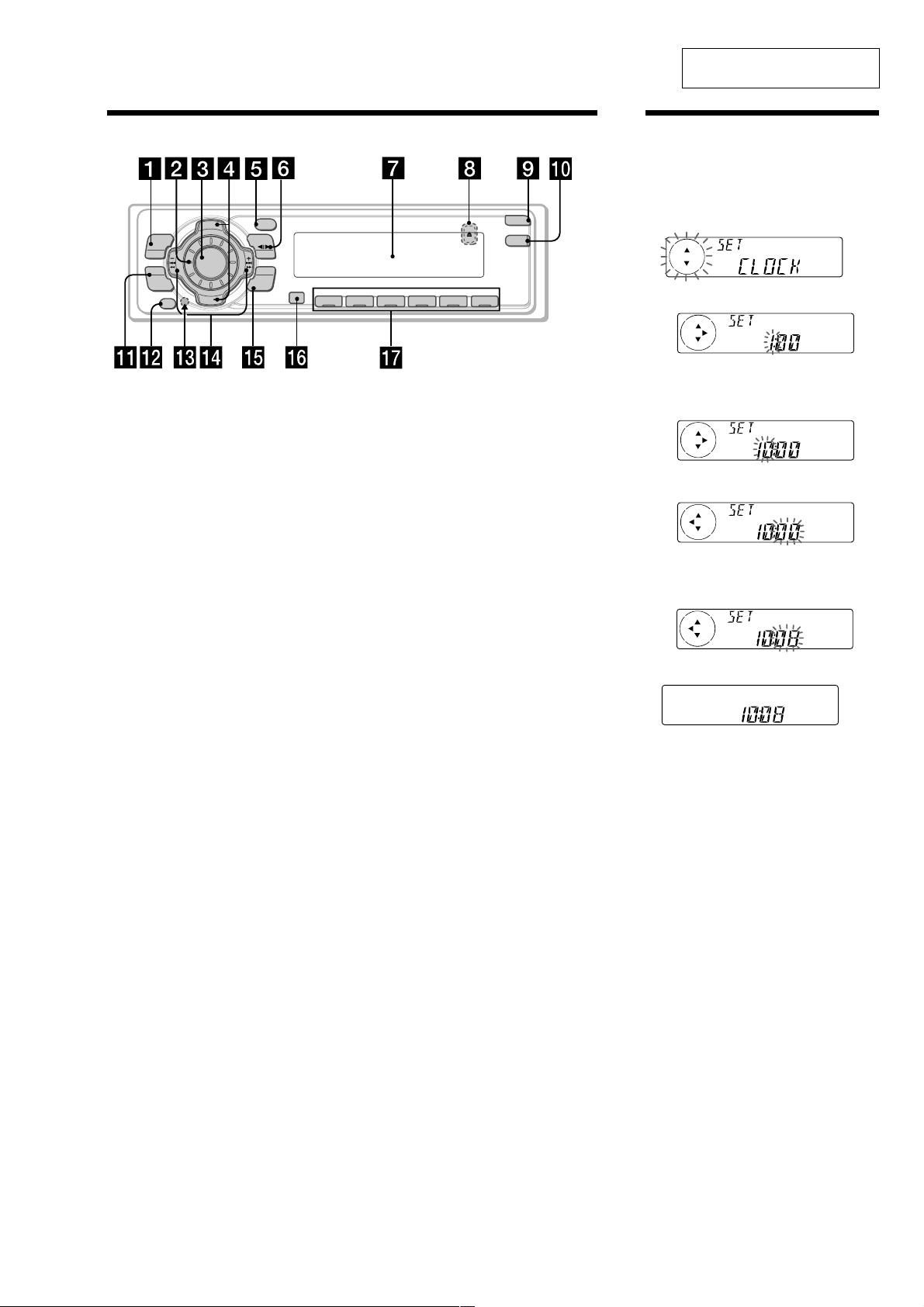
Setting the clock
The clock uses a 12-hour digital indication.
Example: To set the clock to 10:08
1
Press (MENU), then press either side of
(PRST/DISC) repeatedly until “CLOCK”
appears.
1 Press (ENTER).
The hour indication flashes.
2 Press either side of (PRST/DISC) to set
the hour.
3 Press (+) side of (SEEK/AMS).
The minute indication flashes.
4 Press either side of (PRST/DISC) to set
the minute.
2
Press (ENTER).
The clock starts.
After the clock setting is complete, the
display returns to normal playback mode.
Tip
When the D.INFO mode is set to ON, the time is
alwa
s displayed (page 13).
3
Page 4

e
SECTION 2
DISASSEMBLY
Note: Follow the disassembly procedure in the numerical order given.
SUB PANEL, MECHANISM DECK (MG-25F-136)
0
mechanism deck
(MG-25F-136)
8
connector (CN351)
5
sub panel assy
3
screw
(PTT2.6 × 6)
9
screw
(P2.6 × 10)
7
flexible flat cabl
(CN301)
2
two screws
(PTT2.6 × 6)
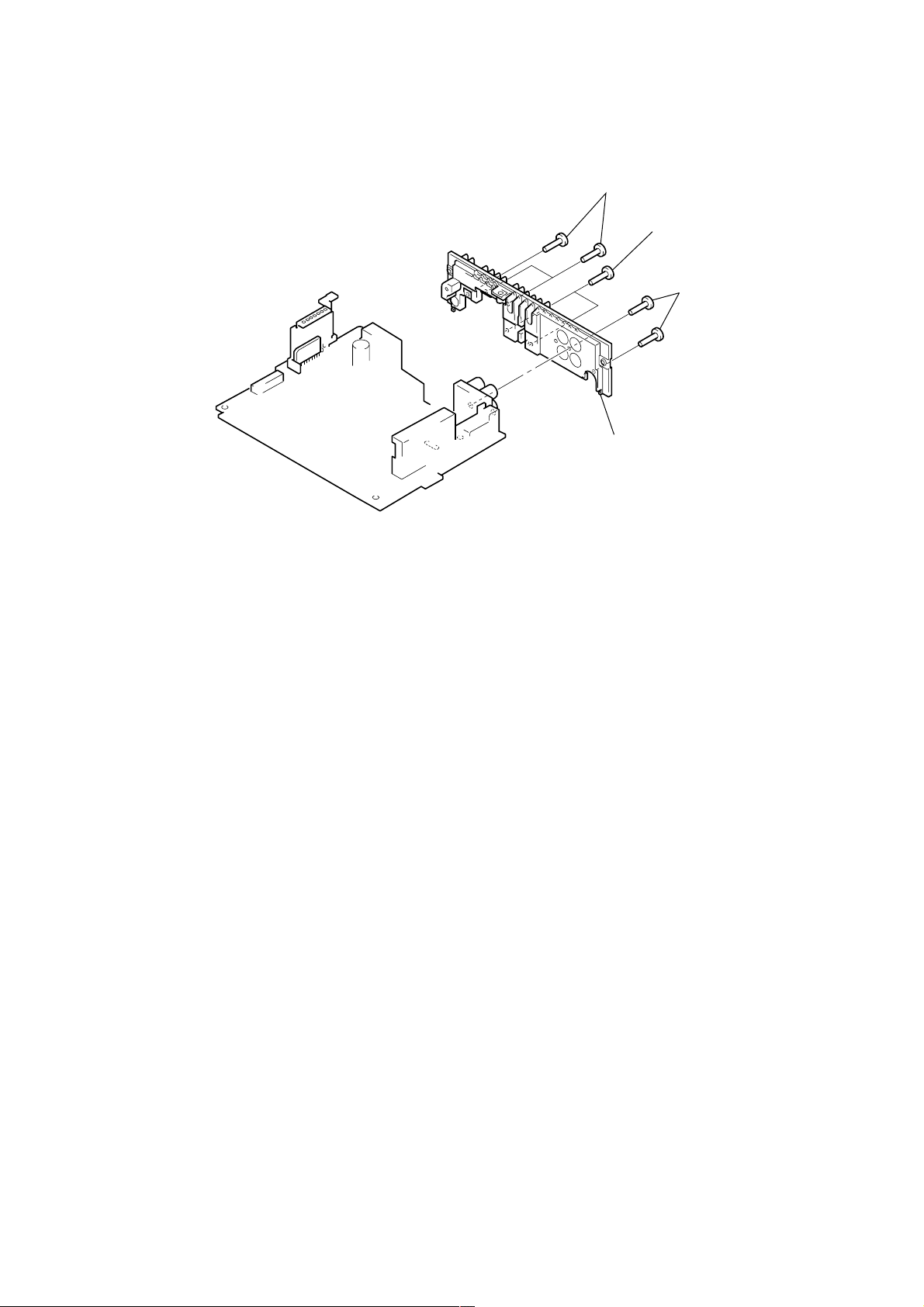
MAIN BOARD
4
2
main board
1
two screws
(PTT2.6 × 6)
two ground point screws
6
flexible flat cable (14 core)
(CN701)
4
screw (PTT2.6 × 6)
3
rubber cap (25)
2
ground point screw
1
three screws
(PTT2.6
×
8)
5
insulated
plate
6
chassis
4
Page 5
HEAT SINK
1
three screws
(PTT2.6
3
heat sink
×
8)
2
two screws
(PTT2.6
1
×
12)
two screws
(PTT2.6
×
8)
5
Page 6
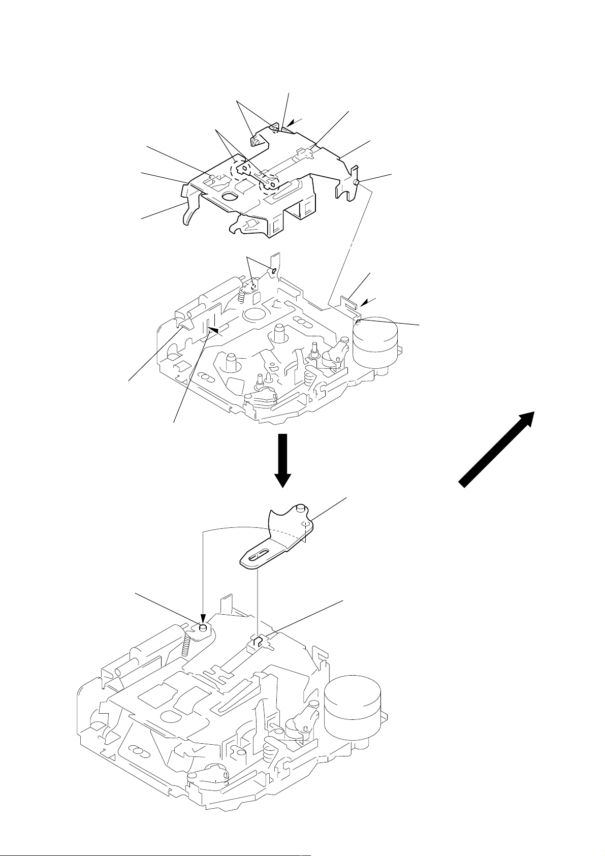
SECTION 3
w
ASSEMBLY OF MECHANISM DECK
Note: Follow the assembly procedure in the numerical order given.
5
HOUSING
4
Fit claw on B part.
3
Put the housing
under A part.
2
Install the hanger onto
two claws of the housing.
housing
Fit projection on C part.
C
part
7
Holder the hanger by bending the claw.
1
Install the catch to the hanger.
hanger
6
Fit projection on D part.
8
Hold the hanger by
bending the claw.
D
part
ARM (SUCTION)
A
part
projection
B
part
2
Move the arm (suction) in the arro
direction and fit on projection.
1
Fit the arm (suction) on the shaft.
6
Page 7
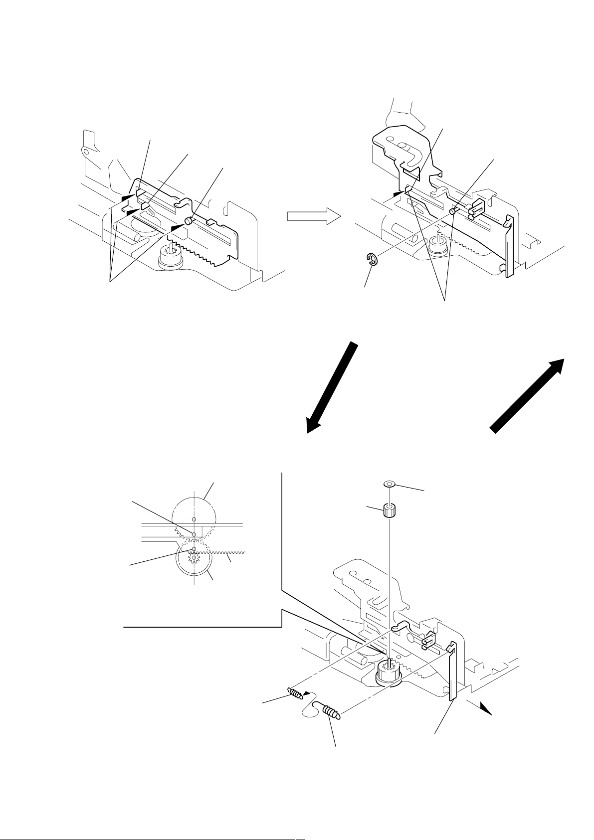
LEVER (LDG-A) / (LDG-B)
)
shaft
A
shaft
1
Fit the lever (LDG-A) on
shafts
A
– C and install it.
B
shaft
C
3
type-E stop ring 2.0
shaft
A
Fit the lever (LDG-B) on
2
shafts
install it.
A
and B and
shaft
B
GEAR (LDG-FT)
hole
hole
gear (LDG-D)
lever (LDG-A)
gear (LDG-FB)
4
Align hole in the gear (LDG-D)
with hole the lever (LDG-A).
2
tension spring (LD-2)
5
gear (LDG-FT)
1
6
polyethylene washer
2
tension spring (LD-1)
3
Move the lever (LDG-B
in the arrow direction.
7
Page 8

GUIDE (C)
s
2
guide (C)
1
three claws
MOUNTING POSITION OF CAPSTAN/REEL MOTOR (M901)
Note: Mount the motor so that the
angle between of the
motor and the hole for the
screw becomes 30
shown in this figure.
°
as
two precision screw
(P2 × 2)
capstan/reel motor
(M901)
30˚
8
Page 9
Tape Speed Adjustment
– SET UPPER VIEW –
SECTION 4
r
MECHANICAL ADJUSTMENTS
SECTION 5
ELECTRICAL ADJUSTMENTS
1. Clean the follo wing parts with a denatured-alcohol-moistened
swab:
playback head pinch roller
rubber belt capstan
idler
2. Demagnetize the playback head with a head demagnetizer.
3. Do not use a magnetized screwdriver for the adjustments.
4. The adjustments should be performed with the power supply
voltage (14.4 V) unless otherwise noted.
• T orque Measurement
Mode Torque Meter Meter Reading
Forward CQ-102C (30 – 65 g•cm)
Forward
Back Tension
Reverse CQ-102RC (30 – 65 g•cm)
Reverse
Back Tension
FF, REW CQ-201B (60 – 200 g•cm)
CQ-102C (0.5 – 4.5g•cm)
CQ-102RC 0.05 – 0.44 mN•m
2.95 – 6.37 mN•m
(0.42 – 0.90 oz•inch)
0.05 – 0.44 mN•m
(0.01 – 0.06 oz•inch)
2.95 – 6.37 mN•m
(0.42 – 0.90 oz•inch)
(0.5 – 4.5g•cm)
(0.01 – 0.06 oz•inch)
5.89 – 19.61 mN•m
(0.83 – 2.78 oz•inch)
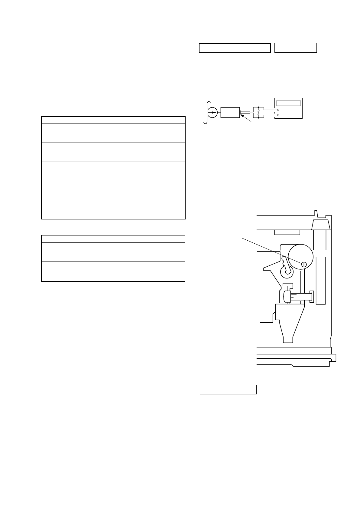
TAPE DECK SECTION
0 dB=0.775 V
Tape Speed Adjustment
Setting:
test tape
WS-48A
(3 kHz, 0 dB)
set
AUDIO OUT REAR jack (J331)
10 k
Ω
frequency counte
+
–
Procedure:
1. Put the set into the FWD PB mode.
2. Adjust adjustment resistor for inside capstan motor so that the
reading on the frequency counter becomes in 3,015 Hz.
Specified Value: 2,955 to 3,075 Hz
Adjustment Location:
• T ape Tension Measurement
Forward CQ-403A (more than 90 g)
Reverse CQ-403R (more than 90 g)
Mode Tension Meter Meter Reading
more than 8.83 mN•m
(more than 3.18 oz)
more than 8.83 mN•m
(more than 3.18 oz)
TUNER SECTION
Tuner section adjustments are done automatically in this set.
9
Page 10

MEMO
10
Page 11

SECTION 6
DIAGRAMS
6-1. BLOCK DIAGRAM – TUNER/T APE/MAIN Section –
J331 (1/2)
BUS
AUDIO IN
L
10511
R-CH
VDD
S-METER
DATA
TAPE
IN2
4
BU B+
TUNER +8V
TUNER +5V
SDA
SCL
131214
CLOCK
+
MUTE
R
FM/MW/SW
HP901
(PLAYBACK)
FWD
L-CH
FWD
R-CH
REV
L-CH
REV
R-CH
J1
ANTENNA
R-CH
1
2
TAPE EQUALIZER AMP, AMS
PBF
IN2
37
R-CH
39
PBR
IN2
R-CH
FM/MW/SW TUNER UNIT
TU1
AM-ANT
FM-ANT
SDA-EEP
SIO
IC301
EQ AMP
R-CH
DRSW
19
TAPESW
18
SCL-EEP
CKO
OUT2
R-CH
FMAGC
PB
EEP VDD
FM-AGC
2
VCC
SW SHIFT
741817
SWSHIFT
INSW
17
AM-IF
R-CH
MPX
NR AMP
8AM-DET
10
19
DOLBY
DOLBY
16 20
R-CH
AMS
DET
MSSW
LINE
OUT2
MS
OUT
XR-C5500T
INPUT SELECT,
ELECTRICAL VOLUME
IC331
SE1L
1
AM
11
SE2L
4
AM-IF
12
13
DATA
CLOCK
7
14
SIO
CKO
FMAGC
MPX
SWSHIFT
AM/FM NOISE
L.P.F
DIGITAL
CONTROL
IIC BUS
SDA
20 21
INPUT
MULTIPLEXER
BLANKER
SCL
LOUDNESS
VOLUME
MUTE
PILOT
CANCELATION
PILOT DET
PLL
SOFT
MUTE
18
DEMODULATOR
STEREO ADJUST
STEREO BLEND
EXT-ATT
TONE
CONTROL
LOUDNESS
OUTPUT
SELECTOR
L.P.F.
D/A
CONVERTER
MPIN
S-METER
1514
MONO
FADER
S & H
BATT B+
OUTLF
MIXER
OUTLR
HIGH-
CUT
D622
MUTING
CONTROL SWITCH
Q622
R-CH
30
29
CONTROL SWITCH
MUTING
Q621
R-CH
R-CH
D625
D621
MUTING
Q171
MUTING
Q271
MUTING
Q181
MUTING
Q281
12
14
11
15
POWER AMP
FL-IN
FR-IN
RL-IN
RR-IN
16
AUX
IC751
22
R-CH
MUTE
FL+
FL–
FR+
FR–
RL+
RL–
RR+
RR–
STNBY
4
5
3
21
23
9
7
17
19
J331(2/2)
L
R
CN781 (1/2)
(POWER CONNECTOR)
1
FRONT L (+)
9
FRONT L (–)
4
FRONT R (+)
12
FRONT R (–)
2
REAR L (+)
10
REAR L (–)
3
REAR R (+)
11
REAR R (–)
AUDIO OUT
(LINE OUT) REAR
LOADING/TAPE
OPERATION
M901
(CAPSTAN/REEL)
05
REEL SENSOR B+
M
M
NROUT
OUT1
9
OUT2
7
LOADING/TAPE OPERATION
CAPSTAN/REEL
MOTOR DRIVE
MOTOR
DRIVE
MOTOR DRIVER
IC351
Q354
MTLON
1
VCC
Q353
IN1
IN2
BATT B+
TAPATT
LMEJ
LMLOD
90 89 91 92
REGULATOR
Q351
REGULATOR
CONTROL SWITCH
3
4
Q352
TAPON
AMSON
BATT B+
74 75 3 77
5752555453
AMSIN
E2P SIO
E2P CKO
MASTER CONTROLLER
IC501 (1/2)
CMON
POS0 – POS3
TAPE OPERATION
EJECT/FF/REW/
REV/FWD MODE DETECT
FMAGC
85 – 88
SWITCH
45
SWSHIFT
I2C SIO
I2C CKO
TAPE
DETECT
REEL SENSOR BOARD
TAKE-UP
REEL
SENSOR
84
BUFFER
4647
REL
SUPPLY
SENSOR
VOLATT
REEL
50
2
VSM
ATT
BEEP
AMPATT
AMPON
35
49
48
BATT B+
• SIGNAL PATH
: FM
: MW/SW
: TAPE PLAY
: BUS AUDIO IN
• R-ch is omitted due to same as L-ch.
1111
Page 12

XR-C5500T
6-2. BLOCK DIAGRAM – DISPLAY/KEY CONTROL/BUS CONTROL/POWER SUPPLY Section –
LIQUID CRYSTAL DISPLAY DRIVER
21
23
22
IC901
64
DI
63
CL
62
CE
60
OSC
4 – 51
S04 – S51
52 – 55
COM1 – COM4
REMOTE CONTROL
RECEIVER
IC951
OSC
C953, R957
LIQUID CRYSTAL
DISPLAY
LCD901
J561
REMOTE IN
LSW801, 901 – 907,
LSW909, 912 – 917,
S901 – 904
RE901
(VOLUME CONTROL)
ROTARY
ENCODER
RE901
D501
D553
24
RCIN1
7
RCIN0
5
KEYIN0
4
KEYIN1
81
REIN0
80
REIN1
MASTER CONTROLLER
IC501 (2/2)
LCDSO
LCDCKO
LCDCE
RST
DATA-OUT
DATA-IN
CLK
BUS ON
BUIN
SIRCS BUFFER
SONY BUS INTERFACE
RST
13
DATA IN
9
DATA OUT
8
CLK IN
11
BUS
ON IN
12
BATT
CHECK
10
Q582
IC581
RESET
SWITCH
BUS ON
SWITCH
BATTERY
SWITCH
RST
DATA
IN/OUT
CLK OUT
BUS ON
OUT
BATT
D587
2
6
4
1
3
CN581
BUS CONTROL IN
(FOR SONY BUS)
3
SIRCS
2
RESET
5
DATA
4
CLK
6
BUS ON
7
BATT
CN901
(FRONT PANEL SIDE)
BU B+
1
RESET SIGNAL
GENERATOR
IC551
KEY ACTIVE
SWITCH
Q551
9
CN701
(MAIN BODY SIDE)
S552
(NOSE DETECT)
BU B+
S551
(RESET)
7
Q601
D581
D572
D582
BATT B+
POWER AMP
(IC751) B+
29
SIRCS
6
8
11
10
9
5
AMP+B
ANT+B
TU+B (8V)
TU+B (5V)
COM8V
BU+B
BATTERY DETECT
Q581
REGULATOR
IC611
TUNER8.7
TUNER5.6
23 4
ILL B+
ACCESSORY CHECK
Q571
VCC
STB
REGULATOR
20
SYSRST
42
UNICKO
BUSON
DOORIND
TUNON
PW ON
OSCOUT
12 13
UNISO
UNISI
UNICLI
BUIN
ILLON
ACCIN
OSCIN
43
44
41
19
28
79
34
36
83
38
82
AD ON
26
KEYACK
78
DOORSW
18
NOSESW
33
RESET
XOUT
XIN
05
16 17
RST
DATA-OUT
DATA-IN
CLK
BUS ON
BUIN
LED801
(TAPE WINDOW),
LSW801
Z
LED DRIVE
Q631
BATT B+
FM/MW/SW TUNER UNIT
(TU1) B+
(AUDIO CIRCUIT B+)
TUNER +8V
TUNER +5V
COM +8V
BU B+
LSW901 – 907, 909, 912 – 917
(ILLUMINATION)
(LCD BACK LIGHT)
REGULATOR
CONTROL SWITCH
D1, 5
D551
LED901 – 904,
LED910 – 913
Q602
TH501
(POWER CONNECTOR)
D610
D611
CN781 (2/2)
6
5
16
7
BATT B+
ANT REM
AMP REM
BATT
ACC
X502
32.768kHz
X501
18.432MHz
1212
Page 13

6-3. NOTE FOR PRINTED WIRING BOARDS AND SCHEMATIC DIAGRAMS
Note on Printed Wiring Board:
• X : parts extracted from the component side.
• Y : parts extracted from the conductor side.
• b : Pattern from the side which enables seeing.
(The other layers' patterns are not indicated.)
Caution:
Pattern face side: Parts on the pattern face side seen from
(Conductor Side) the pattern face are indicated.
Parts face side: Parts on the parts face side seen from
(Component Side) the parts face are indicated.
Note on Schematic Diagram:
• All capacitors are in µF unless otherwise noted. pF: µµF
50 WV or less are not indicated except for electrolytics
and tantalums.
• All resistors are in Ω and
specified.
• C : panel designation.
• U : B+ Line.
• Power voltage is dc 14.4V and fed with regulated dc po wer
supply from ACC and BATT cords.
• Voltages and waveforms are dc with respect to ground
under no-signal (detuned) conditions.
no mark : FM
( ) : AM (MW/SW)
< > : TAPE PLA Y
• Voltages are taken with a VOM (Input impedance 10 MΩ).
Voltage variations may be noted due to normal production tolerances.
• Waveforms are taken with a oscilloscope.
Voltage variations may be noted due to normal production tolerances.
• Circled numbers refer to waveforms.
• Signal path.
F : FM
f : AM (MW/SW)
E : TAPE PLAY
L : BUS AUDIO IN
: Impossible to measure
∗
1
4
/
W or less unless otherwise
• Waveforms
– MAIN Board –
1 IC501 qd (OSCIN)
54.2 ns
2 IC501 qg (XIN)
1.1 Vp-p
2.2 Vp-p
– KEY Board –
1 IC901 y; (OSC)
27
µ
s
2.7 Vp-p
30.5
µ
s
1313
Page 14

XR-C5500T
6-4. SCHEMATIC DIAGRAM – MAIN Board (1/2) – • See page 13 for waveforms. • See page 20 for IC Block Diagrams.
1414
Page 15

6-5. SCHEMATIC DIAGRAM – MAIN Board (2/2) – • See page 20 for IC Block Diagrams.
XR-C5500T
(Page
17)
1515
Page 16

XR-C5500T
6-6. PRINTED WIRING BOARD – MAIN Board –
• Semiconductor
Location
Ref. No. Location
D1 E-9
D51 E-13
D351 I-12
D352 G-13
D501 J-7
D551 F-12
D553 J-10
D571 D-9
D572 D-9
D581 E-11
D582 D-12
D585 B-13
D587 F-10
D588 E-9
D601 J-13
D610 E-10
D611 E-9
D613 D-10
D614 D-10
D621 E-6
D622 D-7
D625 D-7
D701 J-4
D702 J-5
D703 J-5
D704 J-5
D705 J-3
D706 K-5
D707 J-3
D708 J-3
D709 J-3
D710 K-4
D722 D-8
D781 D-12
65
8 7
321
(FRONT VIEW)
4
RR+ RR–
CN781
VIO
TO
GRN
WHT
GRN
VIO
GRY
BLU/WHT
BLU
RED
BLK
GRY
WHT
RED
YEL
2
1
NC
3
NC
4
RL+ RL–
5 6
1 9
2 10
3 11
4 12
5 13
6 14
7 15
8 16
FR+
FR–
1 2
FL+
FL–
3 4
GND
5
AMP REM
6
ACC ANT REM
7
8
BATT NC
9 10
VIO/BLK
GRN/BLK
WHT/BLK
GRN/BLK
VIO/BLK
GRY/BLK
YEL
GRY/BLK
WHT/BLK
BLK
BLU/WHT
BLU
IC301 H-4
IC331 E-4
IC351 I-13
IC501 H-8
IC551 K-11
IC581 D-11
IC611 F-14
IC751 B-7
Q171 C-4
Q181 C-5
Q271 C-5
Q281 D-5
Q351 H-12
Q352 H-12
Q353 H-12
Q354 G-12
Q551 I-11
Q571 D-8
Q581 E-11
Q582 G-10
Q583 E-9
Q601 J-13
Q602 J-13
Q621 E-6
Q622 E-7
Q631 K-6
(Page 17)
1616
Page 17

6-7. PRINTED WIRING BOARD – SUB Board – 6-8. SCHEMATIC DIAGRAM – SUB Board –
(Page 19)
XR-C5500T
(Page 18)
(Page 15)
(Page 16)
1717
Page 18

XR-C5500T
• Semiconductor
Location
Ref. No. Location
IC901 C-6
LED901 A-2
LED902 C-2
LED903 C-3
LED904 A-3
LED910 B-12
LED911 A-12
LED912 A-5
LED913 B-5
6-9. PRINTED WIRING BOARD – KEY Board –
• Semiconductor
Location
Ref. No. Location
D901 A-11
D902 B-10
D903 B-10
D904 B-10
D951 C-4
D952 B-6
IC951 B-8
(Page 17)
1818
Page 19

6-10. SCHEMATIC DIAGRAM – KEY Board – • See page 13 for waveform.
(Page
17)
XR-C5500T
1919
Page 20

• IC Block Diagrams
– MAIN Board –
IC301 CXA2509AQ-T4 IC351 LB1930M-TLM
VCC
1
BUFFER
NC
IN1
IN2
S-GND
2
3
4
BUFFER
5
CONTROL
CIRCUIT
PBFB2
PBRIN2
PBREF2
PBFIN2
VCT
PBGND
PBFIN1
PBREF1
PBRIN1
PBFB1
MSSW
NC
NC
LINEOUT2
MSLPF
25
NR BIAS
TAPE/AUX
TAPE EQ
FWD/RVS
VCC
+
–
F3
–
+
LINEOUT1
DIREF
24dB
NC
10
24dB
G2FB
21222326
MS
MODE
DETECT
MS ON/
OFF
20
19
18
17
16
15
14
13
12
11
MSMODE
DRSW
TAPESW
INSW
NC
NC
MSOUT
DGND
MSTC
G1FB
24
+
–
NC
AUXIN2
PBEQ2
–
31
32
33
34
35
VCT
36
37
38
39
40
F1
1
PBEQ1
TAPEIN2
PBOUT2
GND
282930
27
120µ/70µ
+
F2
–
+
120µ/70µ
345 6 7 8 9
2
VCC
PBOUT1
X1
+
X1
TAPEIN1
T2
LPF
T1
AUXIN1
IC581 BA8270F-E2 IC611 BA4908-V3
BUS ON
1
2
RST
BATT
3
4
CLK
5
VREF
6
DATA
GND
7 8
BUS ON
SWITCH
RESET
SWITCH
BATTERY
SWITCH
14
13
12
11
10
9
VCC
RST
BUS ON
CLK IN
BU IN
DATA IN
DATA OUT
REGULATOR
OVER VOLTAGE
PROTECT
–
+
–
+
MOTOR
DRIVE
CIRCUIT
–
+
IC331 TDA7402TR
NC
10
OUT1
9
8
NC
7
OUT2
P-GND
6
34
ACINLF
35
SWINR
36
SWINL
37
ACOUTR
38
ACOUTL
39
CREF
LP
HP
BASS
TREBLE
VOLUME
SOFTMUTE
LOUDNESS
MUX
40
+
IN-GAIN
+AUTO ZERO
MAIN SOURCE
SELECTOR
MD1
41
MD1G
MD2
MD2G
–
+
MAIN
42
43
PHONO
44
MAIN CH0 AUX
1 2 3 4 5 6 7 8 9 10 11
SEL
SER
ACINLR
ACINRF
ACINRR
33 32 31 30 29 28 27 26 25
LOUDNESS
IN-GAIN
MUTE
SELECTOR
FD2L–
FD2R+
FD2R–
FRONT
REAR
SW
FM
AM
AM
VOICE
BANDPASS
COMPANDER
MIXING
SELECTOR
MULTIPLEXER
FD1L+
FD1L–
ACIN
MAIN
INPUT
FD1R+
SELECTOR
SECOND
FD1R–
OUTPUT
SECOND SOURCE
FD2L+
MONO-
FADER
DIGITAL CONTROL IIC-BUS
OUTLF
MONOFADER
OUTLR
MIXER
MONO-
FADER
BEEP
AM/FM
NOISE BLANKER
OUTRF
OUTRR
MONOFADER
HIGH-CUT
S&H
25kHz
LP
DEMODULATOR
+STEREO ADJUST
+STEREO BLAND
PILOT
CANCELATION
OUTSWL
MONOFADER
SUBWOOFER
+PHASE
CONTROL
PIL DET
PLL
MONO-
FADER
OUTSWR
SUPPLY
PULSE
FORMER
QUAL
MULTIPATH
DETECTOR
D/A
CONVERTER
80kHz
LP
OUTSSL
24 23
OUTSSR
22
VDD
21
SCL
20
SDA
19
GND
18
SM
17
QUAL
16
MPOUT
15
MPIN
14
LEVEL
13
MPX
12
AMIF
2 3
1
NC
TUNER8.7 ANT SW
4
STB
TUNER5.6 SW
5 6 7 8 9 10 1211
ANT
VCC
AMP
VDD5.6V
COM8.7V
TUNER5.6V
GND
TUNER8.7V
2020
Page 21

6-11. IC PIN FUNCTION DESCRIPTION
• MAIN BOARD IC501 MN101C49KTA2 (MASTER CONTROLLER)
Pin No. Pin Name I/O Description
1 VREF I Reference voltage (0V) input terminal (for A/D converter)
2 VSM I
3 FMAGC I FM AGC level detection signal input from the FM/MW/SW tuner unit (TU1) (A/D input)
4 KEYIN1 I
5 KEYIN0 I
6 DSTSEL I Destination setting terminal (fixed at “L” in this set)
7 RCIN0 I Rotary remote commander key input terminal (A/D input)
8 QUALITY I Noise level detection signal input at SEEK mode (A/D input) Not used (open)
9 — O Not used (open)
10 VREF I Reference voltage (+5V) input terminal (for A/D converter)
11 VDD — Power supply terminal (+5V) (for A/D converter)
12 OSCOUT O Main system clock output terminal (18.432 MHz)
13 OSCIN I Main system clock input terminal (18.432 MHz)
14 VSS — Ground terminal (for A/D converter)
15 XIN I Sub system clock input terminal (32.768 kHz)
16 XOUT O Sub system clock output terminal (32.768 kHz)
17 MMOD I Not used (fixed at “L”)
18 NOSESW I
19 BUSON O Bus on/off control signal output to the SONY bus interface (IC581) “L”: bus on
20 SYSRST O Reset signal output to the SONY bus interface (IC581) “L”: reset
21 LCDSO O Serial data output to the liquid crystal display driver (IC901)
22 LCDCE O Chip enable signal output to the liquid crystal display driver (IC901) “H” active
23 LCDCKO O Serial data transfer clock signal output to the liquid crystal display driver (IC901)
24 RCIN1 I Rotary remote commander shift key input terminal “L”: shift
25 RAMBU I
FM and AM signal meter voltage detection input from the FM/MW/SW tuner unit (TU1)
(A/D input)
Key input terminal (A/D input) (LSW801, LSW909, LSW912 to LSW917)
Z, D-BASS, 6, 5, 4, 3, SHUF 2, REP 1 keys input
Key input terminal (A/D input) (LSW901 to LSW907, S901 to S904)
OFF, SOURCE, SOUND, MENU, DSPL, MODE o, ENTER, SEEK/AMS – . m,
PRST + DISC +, SEEK/AMS + > M, PRST – DISC – keys input
Front panel block remove/attach detection signal input
“L”: front panel is attached, “H”: front panel is removed
Internal RAM reset detection signal input terminal
Input terminal to check that RAM data are not destroyed due to low voltage
This checking is made within 50 msec after reset Not used (fixed at “L”)
26 KEYACK I
27 — O Not used (open)
28 BUIN I
29 SIRCS I Sircs remote control signal input form the remote control receiver (IC951)
30, 31 — O Not used (open)
32 MTLIN I Auto metal detection signal input terminal “H”: auto metal Not used (fixed at “L”)
33 RESET I
34 TUNON O
35 BEEP O Beep sound drive signal output to the power amplifier (IC751)
36 PW ON O Main system power supply on/off control signal output to the BA4908 (IC611) “H”: power on
37 COLSEL I Setting terminal for the illumination color “L”: amber, “H”: green Fixed at “H” in this set
Input of acknowledge signal for the key entry Acknowledge signal is input to accept function
and eject keys in the power off status On at input of “H”
Battery detect signal input from the SONY bus interface (IC581) and battery detect circuit
“L” is input at low voltage
System reset signal input from the reset signal generator (IC551) and reset switch (S551)
“L”: reset “L” is input for several 100 msec after power on, then it changes to “H”
Tuner system power supply on/off control signal output to the BA4908 (IC611)
“H”: tuner power on
21
Page 22

Pin No. Pin Name I/O Description
38 ACC IN I Accessory detection signal input “L”: accessory on
39 TESTIN I Setting terminal for the test mode “H”: test mode, Normally: fixed at “L”
40 TELATT I Telephone muting signal input terminal At input of “H”, the signal is attenuated by –20 dB
41 UNICLI I Serial data transfer clock signal input from the SONY bus interface (IC581)
42 UNISO O Serial data output to the SONY bus interface (IC581)
43 UNISI I Serial data input from the SONY bus interface (IC581)
44 UNICKO O Serial data transfer clock signal output to the SONY bus interface (IC581)
45 I2C SIO I/O Two-way data bus with the electrical volume (IC331) and FM/MW/SW tuner unit (TU1)
46 VOLATT O Muting on/off control signal output to the electrical volume (IC331) “L”: muting on
47 I2C CKO O Clock signal output to the electrical volume (IC331) and FM/MW/SW tuner unit (TU1)
48 AMPON O
49 AMPATT O Muting on/off control signal output to the power amplifier (IC751) “L”: muting on
50 ATT O Audio line muting on/off control signal output “H”: muting on
51 TU ATT O
Standby on/off control signal output to the power amplifier (IC751)
“L”: standby mode, “H”: amplifier on
Muting on/off control signal output of the FM and AM tuner signal “H”: muting on
Not used (open)
52 AMSON O
53 NROUT O
54 MTLON I/O
55 TAPATT O
56 DOLON I/O
57 AMSIN I
58 4VPRE I 4VPREOUT model setting terminal “L”: 4VPREOUT model Fixed at “H” in this set
59 to 73 — O Not used (open)
74 E2P SIO I/O Two-way data bus with the FM/MW/SW tuner unit (TU1)
75 E2P CKO O Clock signal output to the FM/MW/SW tuner unit (TU1)
76 — O Not used (open)
77 SWSHIFT O AM filter control signal output to the FM/MW/SW tuner unit (TU1) “L”: SW mode
78 DOORSW I Front panel open/close detection signal input “L” is input when the front panel is closed
79 DOORIND O
80 REIN1 I
81 REIN0 I
82 AD ON O
Tape auto music sensor control signal output to the CXA2509AQ (IC301)
“L” is output to lower the gain for audio level at FF/REW mode
Forward/reverse direction control signal output to the CXA2509AQ (IC301)
“L”: forward direction, “H”: reverse direction
METAL control in/out terminal
At initial mode: auto/manual mode selection input of METAL function (manual at “L” input)
At manual mode: METAL on/off control signal output terminal (METAL on at “H” output)
At auto mode: input at MTLIN (pin es)
Tape muting on/off control signal output to the CXA2509AQ (IC301) “H”: muting on
Active at ATA, FF/REW mode
Dolby control in/out terminal
At initial mode: valid/invalid selection input of dolby function (valid at “L” input)
At normal mode: dolby on/off control signal output terminal (dolby on at “H” output)
Not used this function (fixed at “H”)
Whether a music is present or not from CXA2509AQ (IC301) is detected at auto music sensor
“L”: music is present, “H”: music is not present
LED drive signal output of the tape window and Z indicator (LED801, LSW801)
“H”: LED on “H” is output to turn on LED when front panel is opened
Dial pulse input of the rotary encoder (RE901) (for volume control)
A/D converter power control signal output
When the KEYACK (pin wh) that controls reference voltage power for key A/D conversion input
is active, “L” is output from this terminal to enable the input
83 ILLON O
22
Power on/off control signal output of the illumination LED and liquid crystal display driver
(IC901) “H”: power on
Page 23

Pin No. Pin Name I/O Description
84 REL I
85 POS3 I
86 POS2 I
87 POS0 I
88 POS1 I
89 LMLOD O
Rotation detection signal input from supply reel sensor and take-up reel sensor on the deck
mechanism
Tape position (EJECT/FF/REW/
REV/FWD mode) detection signal
input from the tape operation switch
on the deck mechanism
Motor drive signal output to the loading/tape operation motor driver (IC351) “H” active
(For the loading direction and forward side operation) *1
POS0: “L”: EJECT mode, “H”: others mode
POS1: “L”: FF and FWD mode, “H”: others mode
POS2: “L”: REW mode, “H”: others mode
POS3: “L”: REV and EJECT mode, “H”: others mode
90 LMEJ O
91 TAPON O Tape system power supply on/off control signal output “H”: tape on
92 CMON O Capstan/reel motor (M901) drive signal output “H”: motor on
93, 94 — O Not used (open)
95 DAVSS — Ground terminal (for D/A converter) Not used (open)
96 NS MASK O Discharge control signal output terminal “H”: discharge Not used (open)
97 to 99 — O Not used (open)
100 DAVDD — Power supply terminal (+5V) (for D/A converter) Not used (open)
*1 Loading/tape operation motor control
Mode
Terminal
LMLOD (pin il)
LMEJ (pin o;)
Motor drive signal output to the loading/tape operation motor driver (IC351) “H” active
(For the eject direction and reverse side operation) *1
STOP
“L”“H”“L”“H”
“L”“L”“H”“H”
LOADING/
FORWARD
EJECT/
REVERSE
BRAKE
23
Page 24

SECTION 7
EXPLODED VIEWS
NOTE:
• -XX and -X mean standardized parts, so they
may have some difference from the original
one.
• Color Indication of Appearance Parts
Example:
KNOB, BALANCE (WHITE) . . . (RED)
↑↑
Parts Color Cabinet's Color
(1) CHASSIS SECTION
16
10
not supplied
11
12
27
7
25
#2
#1
#2
#2
• Items marked “*” are not stocked since they
are seldom required for routine service. Some
delay should be anticipated when ordering
these items.
• The mechanical parts with no reference number in the exploded views are not supplied.
• Hardware (# mark) list and accessories and
packing materials are given in the last of the
electrical parts list.
#5
20
MG-25F-136
22
#2
F781
19
21
TU1
#4
16
1
8
9
6
5
4
#10
14
13
3
15
18
#3
#3
#3
#9
17
#3
#3
#3
23
#1
24
Front panel section
Ref. No. Part No. Description Remark
* 1 A-3326-181-A MAIN BOARD, COMPLETE
* 2 3-040-994-01 CHASSIS
* 3 3-045-878-01 PLATE (TU), GROUND
4 X-3377-621-1 LOCK ASSY
5 3-040-990-01 BUTTON (EJECT) (Z)
* 6 1-676-603-11 SUB BOARD
7 3-027-437-11 DOOR, CASSETTE
8 3-935-003-01 SPRING, TORSION
* 9 3-045-877-01 CUSHION (TU)
10 X-3376-699-1 GEAR ASSY
11 3-030-909-01 DAMPER, OIL
12 3-713-786-51 SCREW +P 2X3
* 13 3-045-828-01 INSULATED PLATE
* 14 3-040-996-11 HEAT SINK (2P)
15 3-012-859-01 CAP (25), RUBBER
#2
26
2
Ref. No. Part No. Description Remark
16 3-915-923-01 SCREW, GROUND POINT
17 1-777-184-11 CORD (WITH CONNECTOR) (POWER)
* 18 3-046-991-01 SPACER (COVER R)
* 19 3-046-990-01 SPACER (COVER L)
* 20 3-040-995-01 COVER
* 21 3-040-998-01 BLACKET (IC)
* 22 3-041-262-01 HEAT SINK (REG/XR)
23 1-792-195-11 CABLE, FLEXIBLE FLAT (14 CORE)
24 X-3378-397-1 PANEL ASSY, SUB
25 3-224-530-01 SHEET (L)
26 3-224-529-01 SHEET (R)
27 3-224-528-01 CUSHION
F781 1-532-877-11 FUSE (BLADE TYPE) (AUTO FUSE) (10A)
TU1 A-3220-812-A FM/MW/SW TUNER UNIT (TUX-020)
24
Page 25

(2) FRONT PANEL SECTION
not supplied
(KEY board)
#6
65
66
60
LCD901
61
62
63
64
56
#6
59
58
57
52
51
Ref. No. Part No. Description Remark
51 3-040-980-01 BUTTON (SOURCE)
52 3-040-981-11 KNOB (VOL)
53 3-041-005-11 BUTTON (D) (D-BASS)
54 3-221-784-01 BUTTON (OPEN)
55 3-037-267-01 SPRING (OPEN)
56 3-040-987-01 BUTTON (OFF)
57 3-040-988-01 BUTTON (1-6) (1. 2. 3. 4. 5. 6)
58 3-040-985-01 BUTTON (DIR/ENTER) (MODE o. ENTER)
59 3-040-986-01 BUTTON (MENU/SOUND)
67
55
54
53
Ref. No. Part No. Description Remark
* 60 3-040-997-01 PLATE (LCD), GROUND
* 61 3-041-371-11 SHEET (REFLECTOR)
* 62 3-040-993-01 PLATE (LCD), LIGHT GUIDE
63 1-694-660-11 CONDUCTIVE BOARD, CONNECTION
* 64 3-040-992-01 HOLDER (LCD)
65 X-3378-398-1 PANEL ASSY, FRONT BACK
66 3-045-596-01 CUSHION (OFF)
67 X-3378-581-1 PANEL SUB ASSY
LCD901 1-803-907-11 DISPLAY PANEL, LIQUID CRYSTAL
25
Page 26

(3) MECHANISM DECK SECTION
(MG-25F-136)
153
154
#7
155
158
152
159
157
156
A
A
160
161
163
HP901
162
M901
164
not supplied
168
151
Ref. No. Part No. Description Remark
151 A-3291-667-A CLUTCH (FR) ASSY
* 152 3-019-130-01 LEVER (LDG-A)
* 153 3-019-131-01 LEVER (LDG-B)
154 3-020-539-01 SPRING (LD-1), TENSION
155 3-020-540-01 SPRING (LD-2), TENSION
156 3-020-542-01 GEAR (LOADING FT)
157 3-341-753-11 WASHER, POLYETHYLENE
158 3-020-533-01 HOUSING
* 159 3-020-532-01 ARM (SUCTION)
160 3-020-534-01 HANGER
#8
168
166
167
165
Ref. No. Part No. Description Remark
161 3-933-346-01 CATCHER
162 3-933-344-01 GUIDE (C)
163 3-014-798-01 SCREW (HEAD), SPECIAL
164 3-364-151-01 WASHER
165 A-3220-610-A MECHANISM DECK ASSY
166 3-017-302-01 BELT (25)
167 3-026-636-01 FLYWHEEL (F)
168 3-701-437-21 WASHER
HP901 1-500-157-21 HEAD, MAGNETIC (PLAYBACK)
M901 A-3291-665-A MOTOR ASSY, MAIN (CAPSTAN/REEL)
26
Page 27

SECTION 8
ELECTRICAL PARTS LIST
KEY
NOTE:
• Due to standardization, replacements in the
parts list may be different from the parts specified in the diagrams or the components used
on the set.
• -XX and -X mean standardized parts, so they
may have some difference from the original
one.
• RESISTORS
All resistors are in ohms.
METAL: Metal-film resistor.
METAL OXIDE: Metal oxide-film resistor.
F: nonflammable
Ref. No. Part No. Description Remark Ref. No. Part No. Description Remark
KEY BOARD
**********
1-694-660-11 CONDUCTIVE BOARD, CONNECTION
* 3-040-992-01 HOLDER (LCD)
* 3-040-993-01 PLATE (LCD) , LIGHT GUIDE
* 3-040-997-01 PLATE (LCD) , GROUND
* 3-041-371-11 SHEET (REFLECTOR)
< CAPACITOR >
C951 1-164-004-11 CERAMIC CHIP 0.1uF 10% 25V
C952 1-163-037-11 CERAMIC CHIP 0.022uF 10% 25V
C953 1-163-251-11 CERAMIC CHIP 100PF 5% 50V
C954 1-164-004-11 CERAMIC CHIP 0.1uF 10% 25V
C955 1-164-004-11 CERAMIC CHIP 0.1uF 10% 25V
• Items marked “*” are not stocked since they
are seldom required for routine service.
Some delay should be anticipated when ordering these items.
• SEMICONDUCTORS
In each case, u: µ, for example:
uA. . : µA. . uPA. . : µPA. .
uPB. . : µPB. . uPC. . : µPC. .
uPD. . : µPD. .
• CAPACITORS
uF: µF
• COILS
uH: µH
LED913 8-719-078-19 LED LWA673-R1S2*1 (LCD BACK LIGHT)
LSW901 1-771-609-11 SWITCH, TACT (WITH LED) (OFF)
LSW902 1-762-619-21 SWITCH, KEY BOARD (WITH LED) (SOURCE)
LSW903 1-762-619-21 SWITCH, KEY BOARD (WITH LED) (SOUND)
LSW904 1-762-619-21 SWITCH, KEY BOARD (WITH LED) (MENU)
LSW905 1-762-619-21 SWITCH, KEY BOARD (WITH LED) (DSPL)
LSW906 1-762-619-21 SWITCH, KEY BOARD (WITH LED)
LSW907 1-762-619-21 SWITCH, KEY BOARD (WITH LED) (ENTER)
LSW909 1-762-737-11 SWITCH, KEYBOARD (LED) (D-BASS)
LSW912 1-771-609-11 SWITCH, TACT (WITH LED) (6)
LSW913 1-771-609-11 SWITCH, TACT (WITH LED) (5)
When indicating parts by reference
number, please include the board.
< SWITCH >
(MODE o)
C956 1-164-489-11 CERAMIC CHIP 0.22uF 10% 16V
< CONNECTOR >
CN901 1-794-065-22 PLUG, CONNECTOR 14P
< DIODE >
D901 8-719-158-49 DIODE RD12SB2
D902 8-719-056-82 DIODE UDZ-TE-17-6.2B
D903 8-719-056-82 DIODE UDZ-TE-17-6.2B
D904 8-719-056-82 DIODE UDZ-TE-17-6.2B
D951 8-719-976-99 DIODE DTZ5.1B
D952 8-719-976-99 DIODE DTZ5.1B
< IC >
IC901 8-759-366-34 IC LC75824E
IC951 8-749-012-25 IC RS-170-TU
< LIQUID CRYSTAL DISPLAY >
LCD901 1-803-907-11 DISPLAY PANEL, LIQUID CRYSTAL
< LED >
LED901 8-719-038-07 LED CL-190PG-CD-T (ILLUMINATION)
LED902 8-719-038-07 LED CL-190PG-CD-T (ILLUMINATION)
LED903 8-719-038-07 LED CL-190PG-CD-T (ILLUMINATION)
LED904 8-719-038-07 LED CL-190PG-CD-T (ILLUMINATION)
LED910 8-719-078-19 LED LWA673-R1S2*1 (LCD BACK LIGHT)
LED911 8-719-078-19 LED LWA673-R1S2*1 (LCD BACK LIGHT)
LED912 8-719-078-19 LED LWA673-R1S2*1 (LCD BACK LIGHT)
LSW914 1-771-609-11 SWITCH, TACT (WITH LED) (4)
LSW915 1-771-609-11 SWITCH, TACT (WITH LED) (3)
LSW916 1-771-609-11 SWITCH, TACT (WITH LED) (SHUF 2)
LSW917 1-771-609-11 SWITCH, TACT (WITH LED) (REP 1)
< RESISTOR >
R901 1-216-647-11 METAL CHIP 680 0.5% 1/10W
R902 1-216-647-11 METAL CHIP 680 0.5% 1/10W
R903 1-216-647-11 METAL CHIP 680 0.5% 1/10W
R904 1-216-651-11 METAL CHIP 1K 0.5% 1/10W
R905 1-216-655-11 METAL CHIP 1.5K 0.5% 1/10W
R906 1-216-655-11 METAL CHIP 1.5K 0.5% 1/10W
R907 1-216-659-11 METAL CHIP 2.2K 0.5% 1/10W
R908 1-216-663-11 METAL CHIP 3.3K 0.5% 1/10W
R909 1-216-667-11 METAL CHIP 4.7K 0.5% 1/10W
R910 1-216-671-11 METAL CHIP 6.8K 0.5% 1/10W
R911 1-208-806-11 RES-CHIP 10K 2% 1/10W
R912 1-216-647-11 METAL CHIP 680 0.5% 1/10W
R913 1-216-647-11 METAL CHIP 680 0.5% 1/10W
R914 1-216-647-11 METAL CHIP 680 0.5% 1/10W
R915 1-216-651-11 METAL CHIP 1K 0.5% 1/10W
R916 1-216-655-11 METAL CHIP 1.5K 0.5% 1/10W
R917 1-216-655-11 METAL CHIP 1.5K 0.5% 1/10W
R918 1-216-659-11 METAL CHIP 2.2K 0.5% 1/10W
R919 1-216-663-11 METAL CHIP 3.3K 0.5% 1/10W
R920 1-216-667-11 METAL CHIP 4.7K 0.5% 1/10W
R921 1-216-807-11 METAL CHIP 68 5% 1/16W
R923 1-216-809-11 METAL CHIP 100 5% 1/16W
R925 1-216-021-00 METAL CHIP 68 5% 1/10W
R927 1-216-029-00 METAL CHIP 150 5% 1/10W
27
Page 28

KEY MAIN
Ref. No. Part No. Description Remark
R929 1-216-029-00 METAL CHIP 150 5% 1/10W
R931 1-216-813-11 METAL CHIP 220 5% 1/16W
R932 1-216-813-11 METAL CHIP 220 5% 1/16W
R933 1-216-808-11 METAL CHIP 82 5% 1/16W
R935 1-216-809-11 METAL CHIP 100 5% 1/16W
R938 1-216-809-11 METAL CHIP 100 5% 1/16W
R951 1-216-819-11 METAL CHIP 680 5% 1/16W
R952 1-216-057-00 METAL CHIP 2.2K 5% 1/10W
R953 1-216-857-11 METAL CHIP 1M 5% 1/16W
R954 1-216-049-11 RES-CHIP 1K 5% 1/10W
R955 1-216-049-11 RES-CHIP 1K 5% 1/10W
R956 1-216-821-11 METAL CHIP 1K 5% 1/16W
R957 1-216-851-11 METAL CHIP 330K 5% 1/16W
R958 1-216-033-00 METAL CHIP 220 5% 1/10W
R970 1-216-815-11 METAL CHIP 330 5% 1/16W
R971 1-216-815-11 METAL CHIP 330 5% 1/16W
R972 1-216-864-11 METAL CHIP 0 5% 1/16W
R975 1-216-815-11 METAL CHIP 330 5% 1/16W
R976 1-216-815-11 METAL CHIP 330 5% 1/16W
R981 1-216-864-11 METAL CHIP 0 5% 1/16W
R999 1-216-864-11 METAL CHIP 0 5% 1/16W
< ROTARY ENCODER >
RE901 1-475-014-12 ENCODER, ROTARY (VOLUME CONTROL)
Ref. No. Part No. Description Remark
C102 1-163-263-11 CERAMIC CHIP 330PF 5% 50V
C103 1-163-021-11 CERAMIC CHIP 0.01uF 10% 50V
C104 1-164-489-11 CERAMIC CHIP 0.22uF 10% 16V
C105 1-164-004-11 CERAMIC CHIP 0.1uF 10% 25V
C106 1-109-982-11 CERAMIC CHIP 1uF 10% 10V
C109 1-163-227-11 CERAMIC CHIP 10PF 0.5PF 50V
C110 1-163-227-11 CERAMIC CHIP 10PF 0.5PF 50V
C111 1-163-227-11 CERAMIC CHIP 10PF 0.5PF 50V
C112 1-163-227-11 CERAMIC CHIP 10PF 0.5PF 50V
C141 1-107-823-11 CERAMIC CHIP 0.47uF 10% 16V
C142 1-163-181-00 CERAMIC CHIP 100PF 5% 50V
C171 1-164-506-11 CERAMIC CHIP 4.7uF 16V
C172 1-163-181-00 CERAMIC CHIP 100PF 5% 50V
C174 1-164-489-11 CERAMIC CHIP 0.22uF 10% 16V
C181 1-164-506-11 CERAMIC CHIP 4.7uF 16V
C182 1-163-251-11 CERAMIC CHIP 100PF 5% 50V
C183 1-163-181-00 CERAMIC CHIP 100PF 5% 50V
C184 1-164-489-11 CERAMIC CHIP 0.22uF 10% 16V
C191 1-163-009-11 CERAMIC CHIP 0.001uF 10% 50V
C201 1-163-263-11 CERAMIC CHIP 330PF 5% 50V
C202 1-163-263-11 CERAMIC CHIP 330PF 5% 50V
C203 1-163-021-11 CERAMIC CHIP 0.01uF 10% 50V
C204 1-164-489-11 CERAMIC CHIP 0.22uF 10% 16V
C205 1-164-004-11 CERAMIC CHIP 0.1uF 10% 25V
C206 1-109-982-11 CERAMIC CHIP 1uF 10% 10V
< SWITCH >
S901 1-771-884-11 SWITCH, TACTILE (SEEK/AMS – . m)
S902 1-771-884-11 SWITCH, TACTILE (DISC +, PRST +)
S903 1-771-884-11 SWITCH, TACTILE (SEEK/AMS + > M)
S904 1-771-884-11 SWITCH, TACTILE (DISC –, PRST –)
**************************************************************
* A-3326-181-A MAIN BOARD, COMPLETE
*********************
* 3-040-996-11 HEAT SINK (2P)
* 3-040-998-01 BRACKET (IC)
* 3-041-262-01 HEAT SINK (REG/XR)
7-685-647-79 SCREW +BVTP 3X10 TYPE2 N-S
7-685-793-09 SCREW +PTT 2.6X8 (S)
7-685-795-09 SCREW +PTT 2.6X12 (S)
< CAPACITOR >
C1 1-163-233-11 CERAMIC CHIP 18PF 5% 50V
C2 1-164-004-11 CERAMIC CHIP 0.1uF 10% 25V
C3 1-104-664-11 ELECT 47uF 20% 16V
C5 1-164-004-11 CERAMIC CHIP 0.1uF 10% 25V
C6 1-104-664-11 ELECT 47uF 20% 16V
C8 1-163-009-11 CERAMIC CHIP 0.001uF 10% 50V
C11 1-109-982-11 CERAMIC CHIP 1uF 10% 10V
C13 1-109-982-11 CERAMIC CHIP 1uF 10% 10V
C21 1-164-004-11 CERAMIC CHIP 0.1uF 10% 25V
C22 1-163-037-11 CERAMIC CHIP 0.022uF 10% 25V
C23 1-163-037-11 CERAMIC CHIP 0.022uF 10% 25V
C41 1-163-251-11 CERAMIC CHIP 100PF 5% 50V
C44 1-163-251-11 CERAMIC CHIP 100PF 5% 50V
C52 1-124-234-00 ELECT 22uF 20% 16V
C101 1-163-263-11 CERAMIC CHIP 330PF 5% 50V
C209 1-163-227-11 CERAMIC CHIP 10PF 0.5PF 50V
C210 1-163-227-11 CERAMIC CHIP 10PF 0.5PF 50V
C211 1-163-227-11 CERAMIC CHIP 10PF 0.5PF 50V
C212 1-163-227-11 CERAMIC CHIP 10PF 0.5PF 50V
C241 1-107-823-11 CERAMIC CHIP 0.47uF 10% 16V
C242 1-163-181-00 CERAMIC CHIP 100PF 5% 50V
C271 1-164-506-11 CERAMIC CHIP 4.7uF 16V
C272 1-163-251-11 CERAMIC CHIP 100PF 5% 50V
C274 1-164-489-11 CERAMIC CHIP 0.22uF 10% 16V
C281 1-164-506-11 CERAMIC CHIP 4.7uF 16V
C282 1-163-251-11 CERAMIC CHIP 100PF 5% 50V
C283 1-163-181-00 CERAMIC CHIP 100PF 5% 50V
C284 1-164-489-11 CERAMIC CHIP 0.22uF 10% 16V
C301 1-124-234-00 ELECT 22uF 20% 16V
C302 1-131-353-00 TANTALUM 10uF 10% 35V
C303 1-163-251-11 CERAMIC CHIP 100PF 5% 50V
C304 1-164-004-11 CERAMIC CHIP 0.1uF 10% 25V
C305 1-107-823-11 CERAMIC CHIP 0.47uF 10% 16V
C306 1-163-021-11 CERAMIC CHIP 0.01uF 10% 50V
C307 1-163-021-11 CERAMIC CHIP 0.01uF 10% 50V
C331 1-163-263-11 CERAMIC CHIP 330PF 5% 50V
C332 1-163-017-00 CERAMIC CHIP 0.0047uF 5% 50V
C333 1-163-021-11 CERAMIC CHIP 0.01uF 10% 50V
C335 1-124-233-11 ELECT 10uF 20% 16V
C336 1-164-004-11 CERAMIC CHIP 0.1uF 10% 25V
C337 1-124-584-00 ELECT 100uF 20% 10V
C340 1-107-823-11 CERAMIC CHIP 0.47uF 10% 16V
C341 1-163-181-00 CERAMIC CHIP 100PF 5% 50V
C351 1-165-319-11 CERAMIC CHIP 0.1uF 50V
C352 1-165-319-11 CERAMIC CHIP 0.1uF 50V
C353 1-163-031-11 CERAMIC CHIP 0.01uF 50V
C354 1-124-233-11 ELECT 10uF 20% 16V
C355 1-124-234-00 ELECT 22uF 20% 16V
28
Page 29

MAIN
Ref. No. Part No. Description Remark
C356 1-126-934-11 ELECT 220uF 20% 16V
C357 1-165-319-11 CERAMIC CHIP 0.1uF 50V
C358 1-163-031-11 CERAMIC CHIP 0.01uF 50V
C501 1-124-589-11 ELECT 47uF 20% 16V
C502 1-163-251-11 CERAMIC CHIP 100PF 5% 50V
C503 1-163-227-11 CERAMIC CHIP 10PF 0.5PF 50V
C504 1-163-227-11 CERAMIC CHIP 10PF 0.5PF 50V
C505 1-163-234-11 CERAMIC CHIP 20PF 5% 50V
C506 1-163-235-11 CERAMIC CHIP 22PF 5% 50V
C508 1-164-161-11 CERAMIC CHIP 0.0022uF 10% 100V
C509 1-163-809-11 CERAMIC CHIP 0.047uF 10% 25V
C511 1-163-021-11 CERAMIC CHIP 0.01uF 10% 50V
C551 1-125-710-11 DOUBLE LAYER 0.1F 5.5V
C552 1-104-665-11 ELECT 100uF 20% 10V
C553 1-109-982-11 CERAMIC CHIP 1uF 10% 10V
C556 1-165-319-11 CERAMIC CHIP 0.1uF 50V
C571 1-126-163-11 ELECT 4.7uF 20% 50V
C581 1-164-506-11 CERAMIC CHIP 4.7uF 16V
C582 1-163-009-11 CERAMIC CHIP 0.001uF 10% 50V
C584 1-163-077-00 CERAMIC CHIP 0.1uF 10% 25V
C601 1-164-346-11 CERAMIC CHIP 1uF 16V
C602 1-164-346-11 CERAMIC CHIP 1uF 16V
C611 1-124-233-11 ELECT 10uF 20% 16V
C612 1-124-233-11 ELECT 10uF 20% 16V
C614 1-124-233-11 ELECT 10uF 20% 16V
C615 1-124-233-11 ELECT 10uF 20% 16V
C616 1-124-233-11 ELECT 10uF 20% 16V
C617 1-124-233-11 ELECT 10uF 20% 16V
C618 1-164-506-11 CERAMIC CHIP 4.7uF 16V
C621 1-164-489-11 CERAMIC CHIP 0.22uF 10% 16V
C622 1-124-589-11 ELECT 47uF 20% 16V
C623 1-164-506-11 CERAMIC CHIP 4.7uF 16V
C702 1-163-077-00 CERAMIC CHIP 0.1uF 10% 25V
C703 1-163-077-00 CERAMIC CHIP 0.1uF 10% 25V
C752 1-107-682-11 CERAMIC CHIP 1uF 10% 16V
C753 1-164-506-11 CERAMIC CHIP 4.7uF 16V
C755 1-124-233-11 ELECT 10uF 20% 16V
C756 1-164-506-11 CERAMIC CHIP 4.7uF 16V
C758 1-109-982-11 CERAMIC CHIP 1uF 10% 10V
C781 1-107-885-31 ELECT 3300uF 20% 16V
C782 1-163-077-00 CERAMIC CHIP 0.1uF 10% 25V
C783 1-163-077-00 CERAMIC CHIP 0.1uF 10% 25V
C784 1-163-077-00 CERAMIC CHIP 0.1uF 10% 25V
C785 1-163-077-00 CERAMIC CHIP 0.1uF 10% 25V
Ref. No. Part No. Description Remark
D551 8-719-073-01 DIODE MA111-(K8).S0
D553 8-719-073-01 DIODE MA111-(K8).S0
D571 8-719-057-80 DIODE MA8180-M-TX
D572 8-719-420-14 DIODE MA8082-M
D581 8-719-057-80 DIODE MA8180-M-TX
D582 8-719-017-62 DIODE MA8068-L-TX
D585 8-719-072-70 DIODE MA2ZD14001S0
D587 8-719-911-19 DIODE 1SS119-25
D588 8-719-911-19 DIODE 1SS119-25
D601 8-719-423-23 DIODE MA8110-M
D610 8-719-970-02 DIODE 1SR139-400
D611 8-719-970-02 DIODE 1SR139-400
D613 8-719-970-02 DIODE 1SR139-400
D614 8-719-970-02 DIODE 1SR139-400
D621 8-719-422-12 DIODE MA8039
D622 8-719-073-01 DIODE MA111-(K8).S0
D625 8-719-422-49 DIODE MA8056-L
D701 8-719-035-74 DIODE MA4062-M (TA)
D702 8-719-035-74 DIODE MA4062-M (TA)
D703 8-719-977-12 DIODE DTZ6.8B
D704 8-719-977-12 DIODE DTZ6.8B
D705 8-719-056-82 DIODE UDZ-TE-17-6.2B
D706 8-719-423-23 DIODE MA8110-M
D707 8-719-056-82 DIODE UDZ-TE-17-6.2B
D708 8-719-056-82 DIODE UDZ-TE-17-6.2B
D709 8-719-056-82 DIODE UDZ-TE-17-6.2B
D710 8-719-056-82 DIODE UDZ-TE-17-6.2B
D722 8-719-079-42 DIODE 1ZB22 (TPA3)
D781 8-719-049-38 DIODE 1N5404TU
< IC >
IC301 8-752-079-78 IC CXA2509AQ-T4
IC331 8-759-653-27 IC TDA7402TR
IC351 8-759-527-33 IC LB1930M-TLM
IC501 8-759-688-36 IC MN101C49KTA2
IC551 8-759-682-69 IC XC61CN4302MR
IC581 8-759-449-89 IC BA8270F-E2
IC611 8-759-661-47 IC BA4908-V3
IC751 8-759-690-99 IC TA8268HS
< JACK >
J1 1-764-808-21 JACK (ANT) (FM/MW/SW ANTENNA)
J331 1-774-699-12 JACK, PIN 4P(BUS AUDIO IN,
AUDIO OUT (LINE OUT) REAR)
J561 1-566-822-41 JACK (REMOTE IN)
< CONNECTOR >
CN301 1-785-694-11 CONNECTOR, FFC/FPC 7P
* CN351 1-506-995-11 PIN, CONNECTOR (PC BOARD) 13P
CN581 1-580-907-31 PLUG, CONNECTOR (BUS CONTROL IN)
CN701 1-784-456-11 CONNECTOR, FFC/FPC 14P
CN781 1-774-701-11 PIN, CONNECTOR 16P
< DIODE >
D1 8-719-420-51 DIODE MA729
D51 8-719-420-51 DIODE MA729
D351 8-719-977-22 DIODE DTZ9.1
D352 8-719-970-02 DIODE 1SR139-400
D501 8-719-820-05 DIODE 1SS181
< SHORT >
JC51 1-216-295-11 SHORT 0
JC171 1-216-295-11 SHORT 0
JC181 1-216-295-11 SHORT 0
JC191 1-216-295-11 SHORT 0
JC192 1-216-296-00 SHORT 0
JC193 1-216-296-00 SHORT 0
JC194 1-216-295-11 SHORT 0
JC195 1-216-296-00 SHORT 0
JC271 1-216-295-11 SHORT 0
JC281 1-216-295-11 SHORT 0
JC282 1-216-295-11 SHORT 0
29
Page 30

MAIN
Ref. No. Part No. Description Remark
JC283 1-216-296-00 SHORT 0
JC301 1-216-295-11 SHORT 0
JC302 1-216-295-11 SHORT 0
JC303 1-216-295-11 SHORT 0
JC304 1-216-295-11 SHORT 0
JC351 1-216-295-11 SHORT 0
JC502 1-216-295-11 SHORT 0
JC503 1-216-295-11 SHORT 0
JC504 1-216-295-11 SHORT 0
JC507 1-216-295-11 SHORT 0
JC582 1-216-295-11 SHORT 0
JC583 1-216-296-00 SHORT 0
< COIL >
L51 1-410-750-41 INDUCTOR 0.47uH
L501 1-410-750-41 INDUCTOR 0.47uH
L781 1-419-476-11 COIL, CHOKE 250uH
< TRANSISTOR >
Q171 8-729-920-21 TRANSISTOR DTC314TKH04
Q181 8-729-920-21 TRANSISTOR DTC314TKH04
Q271 8-729-920-21 TRANSISTOR DTC314TKH04
Q281 8-729-920-21 TRANSISTOR DTC314TKH04
Q351 8-729-015-11 TRANSISTOR 2SD1802FAST-TL
Q352 8-729-020-67 TRANSISTOR XN1A312-TX
Q353 8-729-900-53 TRANSISTOR DTC114EK
Q354 8-729-106-60 TRANSISTOR 2SB1115A-YQ
Q551 8-729-027-23 TRANSISTOR DTA114EKA-T146
Q571 8-729-120-28 TRANSISTOR 2SC1623-L5L6
Q581 8-729-900-53 TRANSISTOR DTC114EK
Q582 8-729-027-38 TRANSISTOR DTA144EKA-T146
Q583 8-729-120-28 TRANSISTOR 2SC1623-L5L6
Q601 8-729-423-99 TRANSISTOR 2SD2137-OP
Q602 8-729-020-67 TRANSISTOR XN1A312-TX
Q621 8-729-027-23 TRANSISTOR DTA114EKA-T146
Q622 8-729-120-28 TRANSISTOR 2SC1623-L5L6
Q631 8-729-020-67 TRANSISTOR XN1A312-TX
< RESISTOR >
R1 1-216-025-11 RES-CHIP 100 5% 1/10W
R2 1-216-025-11 RES-CHIP 100 5% 1/10W
R11 1-216-295-11 SHORT 0
R12 1-216-089-11 RES-CHIP 47K 5% 1/10W
R21 1-216-057-00 METAL CHIP 2.2K 5% 1/10W
R22 1-216-085-00 METAL CHIP 33K 5% 1/10W
R101 1-216-041-00 METAL CHIP 470 5% 1/10W
R102 1-216-109-00 METAL CHIP 330K 5% 1/10W
R103 1-216-077-00 RES-CHIP 15K 5% 1/10W
R104 1-216-079-00 METAL CHIP 18K 5% 1/10W
R141 1-216-073-00 METAL CHIP 10K 5% 1/10W
R142 1-216-025-11 RES-CHIP 100 5% 1/10W
R171 1-216-025-11 RES-CHIP 100 5% 1/10W
R172 1-216-081-00 METAL CHIP 22K 5% 1/10W
R173 1-216-025-11 RES-CHIP 100 5% 1/10W
R175 1-216-085-00 METAL CHIP 33K 5% 1/10W
R181 1-216-025-11 RES-CHIP 100 5% 1/10W
R182 1-216-081-00 METAL CHIP 22K 5% 1/10W
R183 1-216-025-11 RES-CHIP 100 5% 1/10W
Ref. No. Part No. Description Remark
R185 1-216-085-00 METAL CHIP 33K 5% 1/10W
R191 1-216-089-11 RES-CHIP 47K 5% 1/10W
R192 1-216-069-00 METAL CHIP 6.8K 5% 1/10W
R201 1-216-041-00 METAL CHIP 470 5% 1/10W
R202 1-216-109-00 METAL CHIP 330K 5% 1/10W
R203 1-216-077-00 RES-CHIP 15K 5% 1/10W
R204 1-216-079-00 METAL CHIP 18K 5% 1/10W
R241 1-216-073-00 METAL CHIP 10K 5% 1/10W
R242 1-216-025-11 RES-CHIP 100 5% 1/10W
R271 1-216-025-11 RES-CHIP 100 5% 1/10W
R272 1-216-081-00 METAL CHIP 22K 5% 1/10W
R273 1-216-025-11 RES-CHIP 100 5% 1/10W
R275 1-216-085-00 METAL CHIP 33K 5% 1/10W
R281 1-216-025-11 RES-CHIP 100 5% 1/10W
R282 1-216-081-00 METAL CHIP 22K 5% 1/10W
R283 1-216-025-11 RES-CHIP 100 5% 1/10W
R285 1-216-085-00 METAL CHIP 33K 5% 1/10W
R301 1-208-812-11 RES-CHIP 18K 2% 1/10W
R302 1-216-097-11 RES-CHIP 100K 5% 1/10W
R303 1-216-065-00 RES-CHIP 4.7K 5% 1/10W
R304 1-216-077-00 RES-CHIP 15K 5% 1/10W
R305 1-216-001-00 METAL CHIP 10 5% 1/10W
R306 1-216-105-00 RES-CHIP 220K 5% 1/10W
R331 1-216-001-00 METAL CHIP 10 5% 1/10W
R332 1-216-089-11 RES-CHIP 47K 5% 1/10W
R333 1-216-025-11 RES-CHIP 100 5% 1/10W
R334 1-216-025-11 RES-CHIP 100 5% 1/10W
R351 1-216-049-11 RES-CHIP 1K 5% 1/10W
R352 1-249-383-11 CARBON 1.5 5% 1/6W
R353 1-216-065-00 RES-CHIP 4.7K 5% 1/10W
R354 1-216-073-00 METAL CHIP 10K 5% 1/10W
R501 1-216-105-00 RES-CHIP 220K 5% 1/10W
R502 1-216-097-11 RES-CHIP 100K 5% 1/10W
R503 1-216-081-00 METAL CHIP 22K 5% 1/10W
R507 1-216-065-00 RES-CHIP 4.7K 5% 1/10W
R508 1-216-065-00 RES-CHIP 4.7K 5% 1/10W
R509 1-216-065-00 RES-CHIP 4.7K 5% 1/10W
R510 1-216-025-11 RES-CHIP 100 5% 1/10W
R511 1-216-073-00 METAL CHIP 10K 5% 1/10W
R512 1-216-097-11 RES-CHIP 100K 5% 1/10W
R513 1-216-073-00 METAL CHIP 10K 5% 1/10W
R514 1-216-025-11 RES-CHIP 100 5% 1/10W
R517 1-216-105-00 RES-CHIP 220K 5% 1/10W
R518 1-216-097-11 RES-CHIP 100K 5% 1/10W
R519 1-216-097-11 RES-CHIP 100K 5% 1/10W
R520 1-216-049-11 RES-CHIP 1K 5% 1/10W
R521 1-216-049-11 RES-CHIP 1K 5% 1/10W
R523 1-216-049-11 RES-CHIP 1K 5% 1/10W
R526 1-216-097-11 RES-CHIP 100K 5% 1/10W
R527 1-216-097-11 RES-CHIP 100K 5% 1/10W
R528 1-216-097-11 RES-CHIP 100K 5% 1/10W
R529 1-216-097-11 RES-CHIP 100K 5% 1/10W
R530 1-216-097-11 RES-CHIP 100K 5% 1/10W
R531 1-216-081-00 METAL CHIP 22K 5% 1/10W
R532 1-216-097-11 RES-CHIP 100K 5% 1/10W
R535 1-249-417-11 CARBON 1K 5% 1/4W
R538 1-216-033-00 METAL CHIP 220 5% 1/10W
30
Page 31

MAIN SUB
Ref. No. Part No. Description Remark
R540 1-216-097-11 RES-CHIP 100K 5% 1/10W
R541 1-216-097-11 RES-CHIP 100K 5% 1/10W
R542 1-216-097-11 RES-CHIP 100K 5% 1/10W
R543 1-216-097-11 RES-CHIP 100K 5% 1/10W
R544 1-216-049-11 RES-CHIP 1K 5% 1/10W
R545 1-216-025-11 RES-CHIP 100 5% 1/10W
R546 1-216-097-11 RES-CHIP 100K 5% 1/10W
R547 1-216-049-11 RES-CHIP 1K 5% 1/10W
R548 1-216-049-11 RES-CHIP 1K 5% 1/10W
R551 1-216-097-11 RES-CHIP 100K 5% 1/10W
R552 1-216-105-00 RES-CHIP 220K 5% 1/10W
R553 1-216-097-11 RES-CHIP 100K 5% 1/10W
R554 1-216-097-11 RES-CHIP 100K 5% 1/10W
R555 1-208-806-11 RES-CHIP 10K 0.5% 1/10W
R556 1-208-806-11 RES-CHIP 10K 0.5% 1/10W
R557 1-216-049-11 RES-CHIP 1K 5% 1/10W
R558 1-216-033-00 METAL CHIP 220 5% 1/10W
R560 1-216-089-11 RES-CHIP 47K 5% 1/10W
R561 1-216-073-00 METAL CHIP 10K 5% 1/10W
R562 1-208-806-11 RES-CHIP 10K 0.5% 1/10W
R563 1-216-025-11 RES-CHIP 100 5% 1/10W
R564 1-216-025-11 RES-CHIP 100 5% 1/10W
R569 1-216-105-00 RES-CHIP 220K 5% 1/10W
R571 1-216-089-11 RES-CHIP 47K 5% 1/10W
Ref. No. Part No. Description Remark
R781 1-216-081-00 METAL CHIP 22K 5% 1/10W
R782 1-216-081-00 METAL CHIP 22K 5% 1/10W
< SWITCH >
S501 1-571-478-11 SWITCH, SLIDE (FREQUENCY SELECT)
S551 1-692-431-21 SWITCH, TACTILE (RESET)
S552 1-771-540-11 SWITCH, PUSH (1 KEY) (NOSE DETECT)
< THERMISTOR >
TH501 1-803-350-21 THERMISTOR, POSITIVE
< TUNER >
TU1 A-3220-812-A FM /MW/SW TUNER UNIT (TUX-020)
< VIBRATOR >
X501 1-781-294-21 VIBRATOR, CRYSTAL (18.432MHz)
X502 1-567-098-41 VIBRATOR, CRYSTAL (32.768kHz)
**************************************************************
* 1-676-603-12 SUB BOARD
**********
1-792-195-11 CABLE, FLEXIBLE FLAT (14 CORE)
R572 1-216-089-11 RES-CHIP 47K 5% 1/10W
R573 1-249-421-11 CARBON 2.2K 5% 1/4W
R574 1-216-081-00 METAL CHIP 22K 5% 1/10W
R576 1-216-105-00 RES-CHIP 220K 5% 1/10W
R580 1-216-025-11 RES-CHIP 100 5% 1/10W
R581 1-216-049-11 RES-CHIP 1K 5% 1/10W
R582 1-216-073-00 METAL CHIP 10K 5% 1/10W
R583 1-216-025-11 RES-CHIP 100 5% 1/10W
R584 1-216-017-00 RES-CHIP 47 5% 1/10W
R585 1-216-089-11 RES-CHIP 47K 5% 1/10W
R586 1-216-073-00 METAL CHIP 10K 5% 1/10W
R587 1-216-073-00 METAL CHIP 10K 5% 1/10W
R588 1-216-097-11 RES-CHIP 100K 5% 1/10W
R589 1-216-085-00 METAL CHIP 33K 5% 1/10W
R594 1-216-049-11 RES-CHIP 1K 5% 1/10W
R601 1-249-387-11 CARBON 3.3 5% 1/4W
R603 1-216-041-00 METAL CHIP 470 5% 1/10W
R604 1-216-041-00 METAL CHIP 470 5% 1/10W
R621 1-216-065-00 RES-CHIP 4.7K 5% 1/10W
R624 1-216-121-11 RES-CHIP 1M 5% 1/10W
R625 1-249-421-11 CARBON 2.2K 5% 1/4W
R631 1-249-417-11 CARBON 1K 5% 1/4W
R632 1-249-417-11 CARBON 1K 5% 1/4W
R701 1-216-049-11 RES-CHIP 1K 5% 1/10W
R702 1-216-025-11 RES-CHIP 100 5% 1/10W
< CONNECTOR >
CNP801 1-794-064-12 SOCKET, CONNECTOR 14P
< LED >
LED801 8-719-038-07 LED CL-190PG-CD-T (TAPE WINDOW)
< SWITCH >
LSW801 1-771-609-11 SWITCH, TACT (WITH LED) (Z)
**************************************************************
MISCELLANEOUS
**************
17 1-777-184-11 CORD (WITH CONNECTOR) (POWER)
23 1-792-195-11 CABLE, FLEXIBLE FLAT (14 CORE)
63 1-694-660-11 CONDUCTIVE BOARD, CONNECTION
F781 1-532-877-11 FUSE (BLADE TYPE) (AUTO FUSE) (10A)
HP901 1-500-157-21 HEAD, MAGNETIC (PLAYBACK)
LCD901 1-803-907-11 DISPLAY PANEL, LIQUID CRYSTAL
M901 A-3291-665-A MOTOR ASSY, MAIN (CAPSTAN/REEL)
************************************************************
**************
HARDWARE LIST
**************
R703 1-216-025-11 RES-CHIP 100 5% 1/10W
R704 1-216-025-11 RES-CHIP 100 5% 1/10W
R705 1-216-025-11 RES-CHIP 100 5% 1/10W
R706 1-216-025-11 RES-CHIP 100 5% 1/10W
R707 1-216-025-11 RES-CHIP 100 5% 1/10W
R708 1-216-025-11 RES-CHIP 100 5% 1/10W
R710 1-216-001-00 METAL CHIP 10 5% 1/10W
R751 1-216-049-11 RES-CHIP 1K 5% 1/10W
R753 1-216-073-00 METAL CHIP 10K 5% 1/10W
#1 7-621-772-20 SCREW +B 2X5
#2 7-685-792-09 SCREW +PTT 2.6X6 (S)
#3 7-685-793-09 SCREW +PTT 2.6X8 (S)
#4 7-685-647-79 SCREW +BVTP 3X10 TYPE 2 N-S
#5 7-685-791-09 SCREW +PTT 2.6X5 (S)
#6 7-685-106-19 SCREW +P 2X10 TYPE 2 NON-SLIT
#7 7-624-104-04 STOP RING 2.0 TYPE-E
#8 7-627-553-17 PRECISION SCREW +P 2X2 TYPE 3
#9 7-685-795-09 SCREW +PTT 2.6X12 (S)
31
Page 32

XR-C5500T
Ref. No. Part No. Description Remark
#10 7-627-553-28 PRECISION SCREW +P 2X2.5
************************************************************
ACCESSORIES & PACKING MATERIALS
*******************************
3-227-562-11 MANUAL, INSTRUCTION (ENGLISH, ARABIC)
************************************************************
501 1-777-184-11 CORD (WITH CONNECTOR) (POWER)
502 3-023-953-11 SCREW, +T (5X8) TAPPING
X-3378-490-1 CASE (PANEL) ASSY
PARTS FOR INSTALLATION AND CONNECTIONS
**************************************
501 502
POWER CORD
+T5 × 8
(× 4)
Ref. No. Part No. Description Remark
9-870-229-11
32
Sony Corporation
Audio Entertainment Group
Printed in Japan C 2000. 12
2000L05XXX3-1
Published by General Engineering Dept.
 Loading...