

Sony UWP-V1,UWP-X8,UWP-V2,UWP-X7,UWP-V6 Service Manual

UHF WIRELESS MICROPHONE PACKAGE
UWP-V1
UWP-V2
UWP-V6
UWP-X7
UWP-X8
UHF SYNTHESIZED TRANSMITTER
UTX-B2
UHF SYNTHESIZED WIRELESS MICROPHONE
UTX-H2
UHF SYNTHESIZED TUNER UNIT
URX-M2
UHF SYNTHESIZED DIVERSITY TUNER
URX-P2
UHF SYNTHESIZED TRANSMITTER
UTX-P1
SERVICE MANUAL
1st Edition

! WARNING
This manual is intended for qualified service personnel only.
To reduce the risk of electric shock, fire or injury, do not perform any servicing other than that
contained in the operating instructions unless you are qualified to do so. Refer all servicing to
qualified service personnel.
! WARNUNG
Die Anleitung ist nur für qualifiziertes Fachpersonal bestimmt.
Alle Wartungsarbeiten dürfen nur von qualifiziertem Fachpersonal ausgeführt werden. Um die
Gefahr eines elektrischen Schlages, Feuergefahr und Verletzungen zu vermeiden, sind bei
Wartungsarbeiten strikt die Angaben in der Anleitung zu befolgen. Andere als die angegeben
Wartungsarbeiten dürfen nur von Personen ausgeführt werden, die eine spezielle Befähigung
dazu besitzen.
! AVERTISSEMENT
Ce manual est destiné uniquement aux personnes compétentes en charge de l’entretien. Afin
de réduire les risques de décharge électrique, d’incendie ou de blessure n’effectuer que les
réparations indiquées dans le mode d’emploi à moins d’être qualifié pour en effectuer d’autres.
Pour toute réparation faire appel à une personne compétente uniquement.
UWP Series

Table of Contents
1. Service Overview
1-1. UTX-B2 .......................................................................... 1-1
1-1-1. Disassembly .......................................................... 1-1
1-1-2. Precaution for Reassembling ................................. 1-2
1-1-3. Precaution When Replacing EEPROM (IC611) ... 1-3
1-1-4. Error Messages ......................................................1-3
1-2. UTX-H2 ..........................................................................1-4
1-2-1. Disassembly .......................................................... 1-4
1-2-2. Precaution When Replacing EEPROM (IC401) ... 1-6
1-2-3. Error Messages ......................................................1-6
1-3. URX-M2 ......................................................................... 1-7
1-3-1. Removal/Installation ............................................. 1-7
1-3-2. URX-M2 Checking ............................................. 1-10
1-3-3. Error Messages ....................................................1-10
1-4. URX-P2 ........................................................................ 1-11
1-4-1. Disassembly ........................................................ 1-11
1-4-2. Precaution for Reassembling ............................... 1-12
1-4-3. Precaution When Replacing EEPROM (IC11) ... 1-13
1-4-4. Error Messages ....................................................1-13
1-5. UTX-P1 ......................................................................... 1-14
1-5-1. Disassembly ........................................................ 1-14
1-5-2. Precaution for Reassembling ............................... 1-15
1-6. Unleaded Solder ............................................................ 1-15
2. Electrical Alignment
2-1. UTX-B2 .......................................................................... 2-1
2-1-1. Equipment and Tools ............................................ 2-1
2-1-2. Adjustments ........................................................... 2-2
2-2. UTX-H2 ........................................................................2-13
2-2-1. Equipment and Tools .......................................... 2-13
2-2-2. Adjustments ......................................................... 2-14
2-3. URX-M2 ....................................................................... 2-26
2-3-1. Equipment and Tools .......................................... 2-26
2-3-2. Adjustments ......................................................... 2-27
2-4. URX-P2 ........................................................................ 2-40
2-4-1. Equipment and Tools .......................................... 2-40
2-4-2. Adjustments ......................................................... 2-41
2-5. UTX-P1 ......................................................................... 2-56
2-5-1. Equipment and Tools .......................................... 2-56
2-5-2. Adjustments ......................................................... 2-57
3. Spare Parts
3-1. Notes on Repair Parts ..................................................... 3-1
3-2. Exploded Views ..............................................................3-2
3-2-1. UTX-B2 ................................................................. 3-2
3-2-2. UTX-H2 ................................................................ 3-4
3-2-3. URX-M2 ................................................................ 3-6
3-2-4. URX-P2 .................................................................3-8
3-2-5. UTX-P1 ............................................................... 3-10
3-3. Electrical Parts List .......................................................3-12
3-3-1. UTX-B2 ............................................................... 3-12
3-3-2. UTX-H2 .............................................................. 3-17
3-3-3. URX-M2 .............................................................. 3-21
3-3-4. URX-P2 ...............................................................3-28
3-3-5. UTX-P1 ............................................................... 3-36
3-4. Accessories Supplied .................................................... 3-40
3-4-1. UWP-V1 ..............................................................3-40
3-4-2. UWP-V2 ..............................................................3-40
3-4-3. UWP-V6 ..............................................................3-41
3-4-4. UWP-X7 ..............................................................3-41
3-4-5. UWP-X8 ..............................................................3-41
4. Block Diagrams and Circuit Descriptions
4-1. UTX-B2 .......................................................................... 4-2
4-2. UTX-H2 ..........................................................................4-4
4-3. URX-M2 ......................................................................... 4-6
4-4. URX-P2 .......................................................................... 4-8
4-5. UTX-P1 ......................................................................... 4-10
5. Board Layouts
5-1. UTX-B2 .......................................................................... 5-1
5-2. UTX-H2 ..........................................................................5-2
5-3. URX-M2 ......................................................................... 5-3
5-4. URX-P2 .......................................................................... 5-4
5-5. UTX-P1 ........................................................................... 5-5
6. Schematic Diagrams
6-1. UTX-B2 .......................................................................... 6-1
6-2. URX-H2 .......................................................................... 6-4
6-3. URX-M2 ......................................................................... 6-5
6-4. URX-P2 .......................................................................... 6-9
6-5. UTX-P1 ......................................................................... 6-14
UWP Series
1

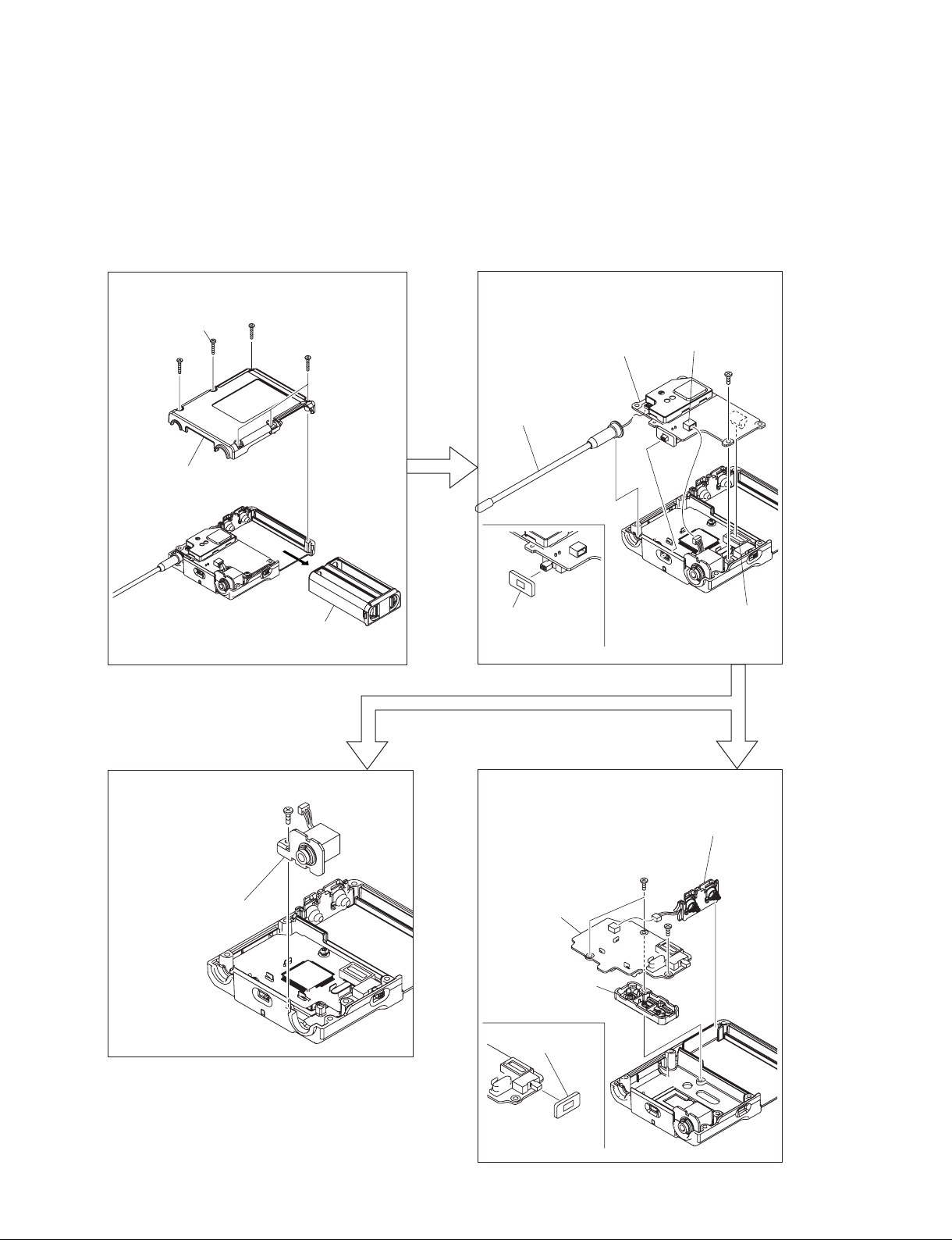
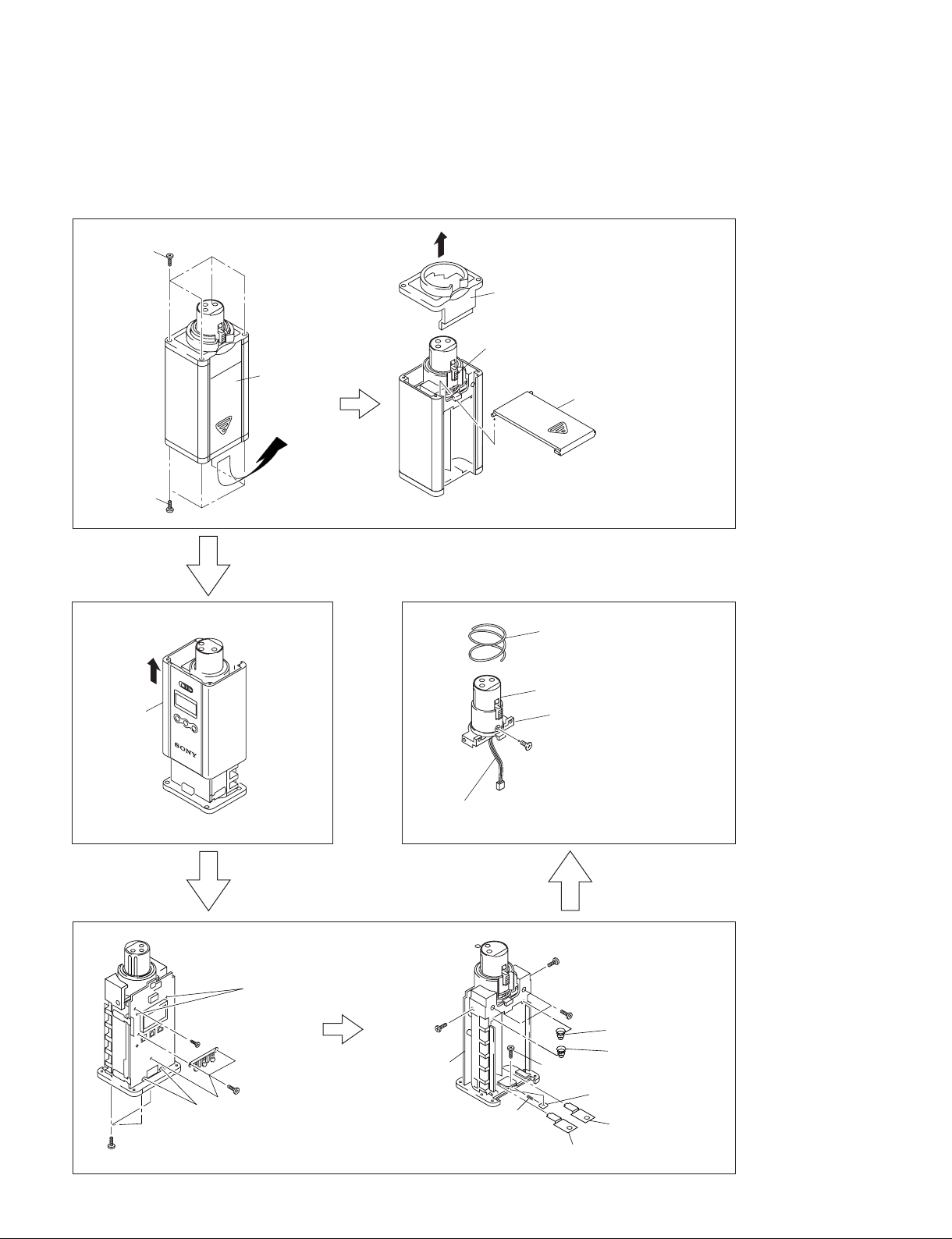
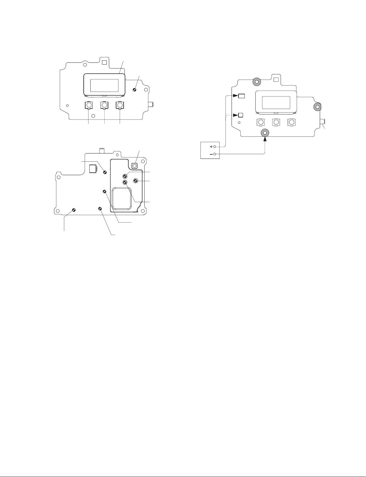
1-1. UTX-B2
1-1-1. Disassembly
Section 1
Service Overview
Rear cabinet (TX)
M2 x 10
M2 x 10
Rear cabinet (TX)
M2 x 10
M2 x 10
Battery case assembly
Antenna/CPU-422 board
CPU422 board
Antenna
Mic sheet
Be careful not to
drop or lose this.
CN401
P2 x 5
CN2
Stereo miniature jack
UWP Series
P2 x 5
RF-131 boardStereo miniature jack
Battery spring plate
P2 x 5
RF-131 board
P2 x 5
Set button
Power protection
sheet
Be careful not to
drop or lose this.
1-1
1-1-2. Precaution for Reassembling
When reassembling the UTX-B2, arrange the battery harnesses as shown in the following figures.
Battery spring
(Black)
(Red)
Harness
Battery spring plate
Arranging the harnesses as shown in the figures.
Tape for insulation
Front side Rear side
Front
cabinet
Note
When reassembling the UTX-B2, be careful that
the harness must not be pinched.
1-2
UWP Series

1-1-3. Precaution When Replacing EEPROM (IC611)
When the EEPROM (IC611) is replaced with the new EEPROM, the same data that have been stored in
the removed EEPROM must be written into the newly mounted EEPROM.
1-1-4. Error Messages
When an error occurs, any of the following error messages can be generated by the self-diagnostics
function that is built-in the UTX-B2 and can appear on the display section.
Message Error contents Remedial measure
Err01 An error occurs in the backup With “Err01” displayed, press and hold the “-“ button
Err02 An error occurs in the PLL Check the PLL synthesizer circuit (IC301, CP321 on
Err03 Power supply voltage has exceeded Use the equipment with the power supply of the
INIT The message is displayed when Do not press the “SET” button and the “_“ button.
memory data. for 20 seconds to read the backup data.
The data is successfully read when “RELOAD” is
displayed. If the data fails to be read, check the
EEPROM (IC661) and its peripheral circuits, and write
the frequency data to the EEPROM.
synthesizer circuit. the RF-131 board and its peripheral circuits).
the range of allowable limits. specified voltage range.
the power is turned on while the
“SET” button and the “_“ button are
pressed at the same time.
If the “SET” button and the “_“ button
are pressed at the same time, the
UTX-B2 enters the default setting mode.
UWP Series
1-3
1-2. UTX-H2
1-2-1. Disassembly
Cage sub assembly
Cage sub assembly
Model cover
Grip (B)
*Grip removal fixture
Grip (B)
Grip (B)
Ring stopper
Dynamic unit
Do not touch the portion
during removing the unit.
Connector (3P)
Dynamic unit
Remove it using
tweezers.
Connector
(3P)
*Grip removal fixture
* : Tools required :
Grip removal fixture (J-6407-080-A)
Push up the claws.
(If difficult to remove,
unlock one claw
after another.)
Go to page 1-5
(Grip A)
1-4
UWP Series
Grip (A) Antenna/MB-1137 board
Indicator
Power button
Power lock
Precision
P2.6 x 5
Stopper
Disengage the claw of
the chassis (A) using
a flat head (_) screwdriver,
and remove the stopper.
Protruded portion
of the indicator
*LRT screw
(M2 x 4)
Hole
Precision
P2 x 3
Grip (A)
Stopper
Claw of
the chassis (A)
Chassis (A)
assembly
Remove the chassis (A)
assembly in the direction of
the arrow in the way as if
removing the protruded
portion of the indicator.
MB-1137 board
Unsolder.
Precision
P2 x 3
Antenna
Chassis (B) sub
assembly
Precision
P2 x 3
Precision
P2 x 3
Shield
Unsolder.
Three claws
UWP Series
*: Tools required :
LRT screwdriver (J-6402-350-A)
Three claws
Chassis (A) sub assembly
1-5

1-2-2. Precaution When Replacing EEPROM (IC401)
When the EEPROM (IC401) is replaced with the new EEPROM, the same data that have been stored in
the removed EEPROM must be written into the newly mounted EEPROM.
1-2-3. Error Messages
When an error occurs, any of the following error messages can be generated by the self-diagnostics
function that is built-in the UTX-H2 and can appear on the display section.
Message Error contents Remedial measure
Err01 An error occurs in the backup Check the EEPROM (IC401) and its peripheral
Err02 An error occurs in the PLL Check the PLL synthesizer circuit (IC102, CP101 on
Err03 Power supply voltage has exceeded Use the equipment with the power supply of the
memory data. circuits.
synthesizer circuit. the MB-5 board and its peripheral circuits).
the range of allowable limits. specified voltage range.
1-6
UWP Series
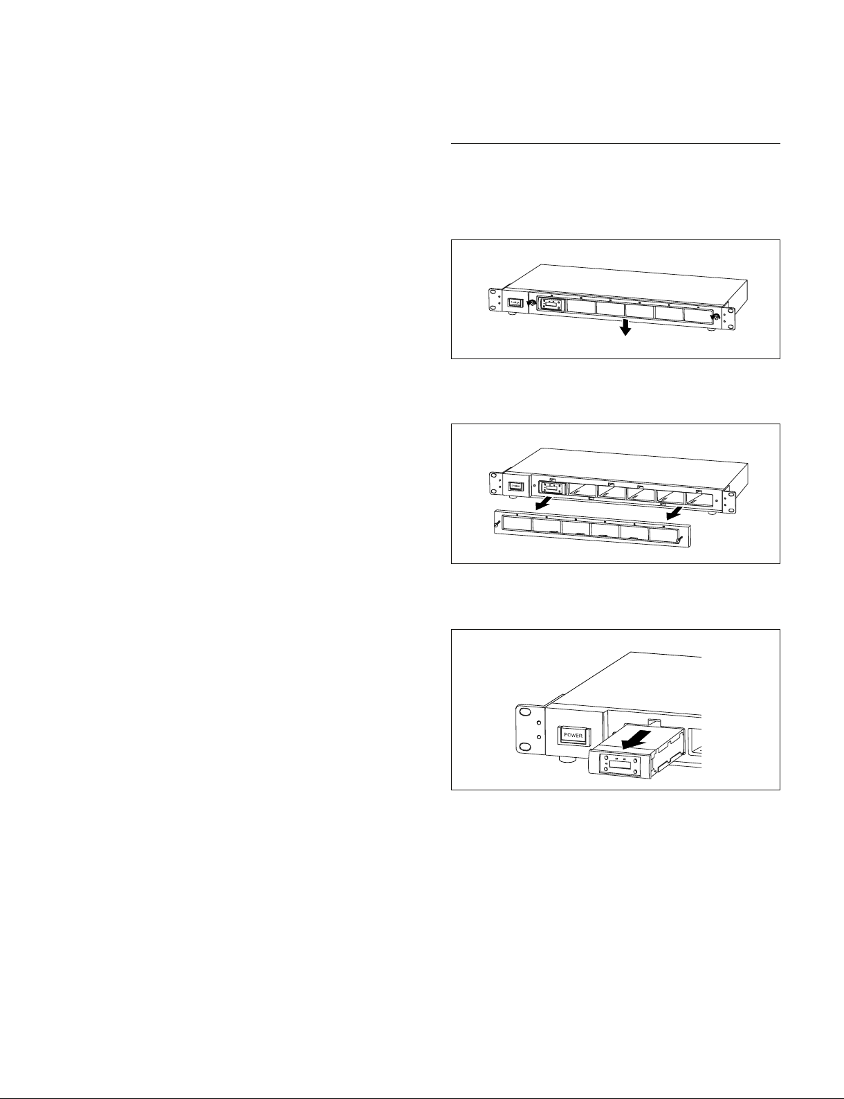
1-3. URX-M2
1. Tuner Base Unit MB-X6 / MB-806A
1-3-1. Removal/Installation
m
Before installing the URX-M2, make sure the MB-806A
.
into which the URX-M2 will be installed is turned off. Do
not install or uninstall the URX-M2 while the MB-806A is
turned on, as this may damage the connector or cause noise.
. The buttons and display on the front panel of the URX-
M2 may be damaged if they are gripped too strongly.
Always hold the URX-M2 by the side.
. Do not put your fingers on the connectors on the rear
panel of the URX-M2 or into the slot on the unit into
which the URX-M2 will be installed.
. Keep the URX-M2 away from static electricity.
When using the MB-X6
Removal
1. Loosen the screws at both sides of the front cover, then
slide the front cover downward.
2. Hold the screws by the head and pull forward to
remove the front cover.
3. Remove the tuner unit URX-M2 from the slot in the
direction of the arrow.
UWP Series
1-7
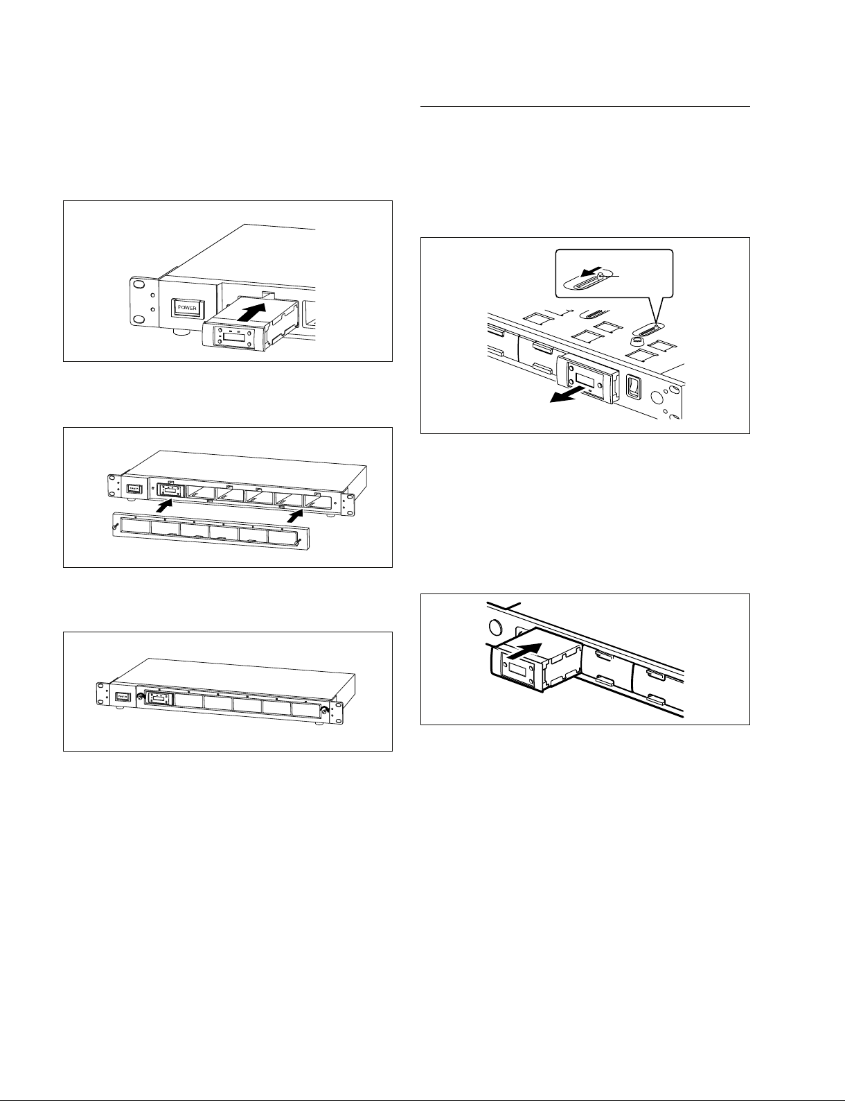
Installation
When using the MB-806A
1. After removing the front cover, hold the tuner unit by
the top and bottom, then insert the tuner unit into the
slot.
2. Match the six latches with the six holes on the front
panel, then replace the front cover.
3. Tighten the screws on the front cover to secure it to the
front panel of the MB-X6.
Removal
1. On the bottom panel of the MB-806A, locate the lever
corresponding to the slot of the URX-M2 to be
removed and pull the lever forward. The URX-M2 is
ejected from the slot.
Lever
Installation
The MB-806A Tuner Base Unit can accommodate up to 6
URX-M2.
1. Inspect the top and bottom side of the URX-M2.
2. Holding both sides of the URX-M2, insert it into the
slot. Push it in until you hear a click.
1-8
UWP Series
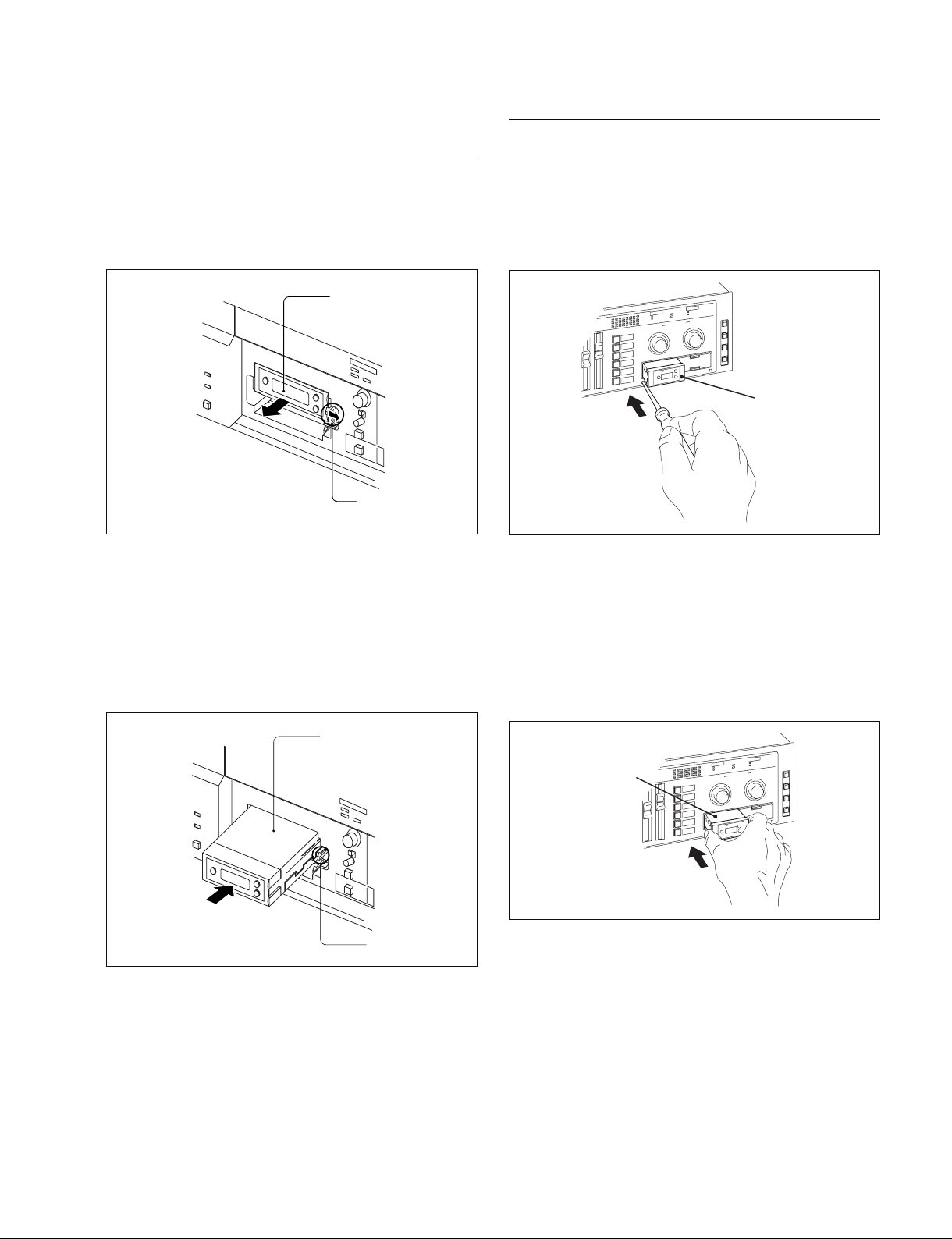
GP
AF
R
F
GP
CH
B
ATT
2. Powered Mixer SRP-X500P / SRP-X700P
When using the SRP-X700P
When using the SRP-X500P
Removal
1. Pull the latch securing the tuner unit to the side and
pull out the tuner unit URX-M2.
URX-M2
Latch
Installation
1. Check the top and bottom sides of the tuner unit, and
then insert it into the slot.
n
When installing the tuner unit, insert it fully into the
tuner slot of the SRP-X500P and secure it with the
latch on the slot.
Removal
1. Insert a screwdriver into the hole under the lower part
of the tuner slot and remove the URX-M2.
Screwdriver : Shaft diamter is between 2 to 4 mm
Shaft length is 30 mm or longer
SCENE
ECALL
R
B
MASTER
A
LINE 4 SELECT
A
B
C
D
E
F
ATT
B
RF
URX-M2
Installation
The SRP-X700P Powered Mixer can accommodate up to 2
URX-M2.
1. Remove the tuner slot cover from the SRP-X700P and
inspect the top and bottom sides of the URX-M2.
2. Holding the tuner module on both sides, insert it into
the slot.
URX-M2
URX-M2
LINE 4 SELECT
A
B
C
D
E
F
MASTER
A
TT
A
B
F
A
GP
F
R
H
C
P
G
SCENE
RECALL
B
Latch
UWP Series
1-9

1-3-2. URX-M2 Checking
The following procedures describe how to prove URX-M2 whether it needs to be required or not.
Equipment Required : MB-X6 (quality unit) / MB-806A (quality unit)
URX-M2 (quality unit)
1. Install the URX-M2 (repair unit) to be checked in an MB-X6 / MB-806A (quality unit).
2. Check if there is any fault using the MB-X6 / MB-806A (quality unit).
. If there is a fault, URX-M2 is defective.
Check the URX-M2 then fix a faulty section, and perform “2. Electrical Alignment”.
. If there is no fault, the URX-M2 (repair unit) is not defective. The original MB-X6 / MB-806A on
which the URX-M2 (repair unit) had been mounted is defective.
1-3-3. Error Messages
When an error occurs, any of the following error messages can be generated by the self-diagnostics
function that is built-in the URX-M2 and can appear on the display section.
Message
Err01
Err02
Err03
NOTONE
Sq OFF
Error contents
An error occurs in EEPROM data.
The PLL synthesizer circuit does not
lock.
Power supply voltage has exceeded
the range of allowable limits.
The tone signal does not exist, or
any tone signal radio wave other
than 32 kHz is received and the
audio signal is muted.
If you turn on the power while
pressing the “SET” button and the
“_” button at the same time, the
squelch function release mode is
set, and this message appears once
before the display of normal
operation appears.
Remedial measure
Take both of the following remedial measures.
. Write the frequency data that corresponds to the
desired destination location, into EEPROM.
. Perform the RF squelch adjustment and the RF
level indicator adjustment. (Refer to Section 2-3.)
If the frequency data that does not corresponds to
the desired reception frequency range is written:
Write the correct frequency data into the EEPROM.
If the error message is displayed even though the
frequency data is correct:
Check the PLL synthesizer circuit (IC301, X301,
Q305 and Q306 and its peripheral circuits on the
MB-1129 board).
Use the equipment with the power supply of the
specified voltage range.
An interference radio wave has occurred in the
frequency band in use.
. If an error is displayed while the power of the
transmitter is on:
Turn off the power of the transmitter.
. If the RF level indicator of the receiver LCD lights
even when the power of the transmitter is turned off:
Set the frequency of the transmit/receive channel
that is free from the interference radio wave.
When the error is not caused by the signal interference, the tone squelch circuit of receiver or transmitter
(both receiver and transmitter) is defective.
. Check the receiver : Check the tone squelch.
(Refer to Section 2-3.)
If the tone squelch does
not work well, check the
tone squelch circuit (IC406
and its peripheral circuit
on the MB-1129 board.)
. Check the transmitter : Refer to the Service
Manual of transmitter.
Turn off the power once and then back on without
pressing any button.
1-10
UWP Series
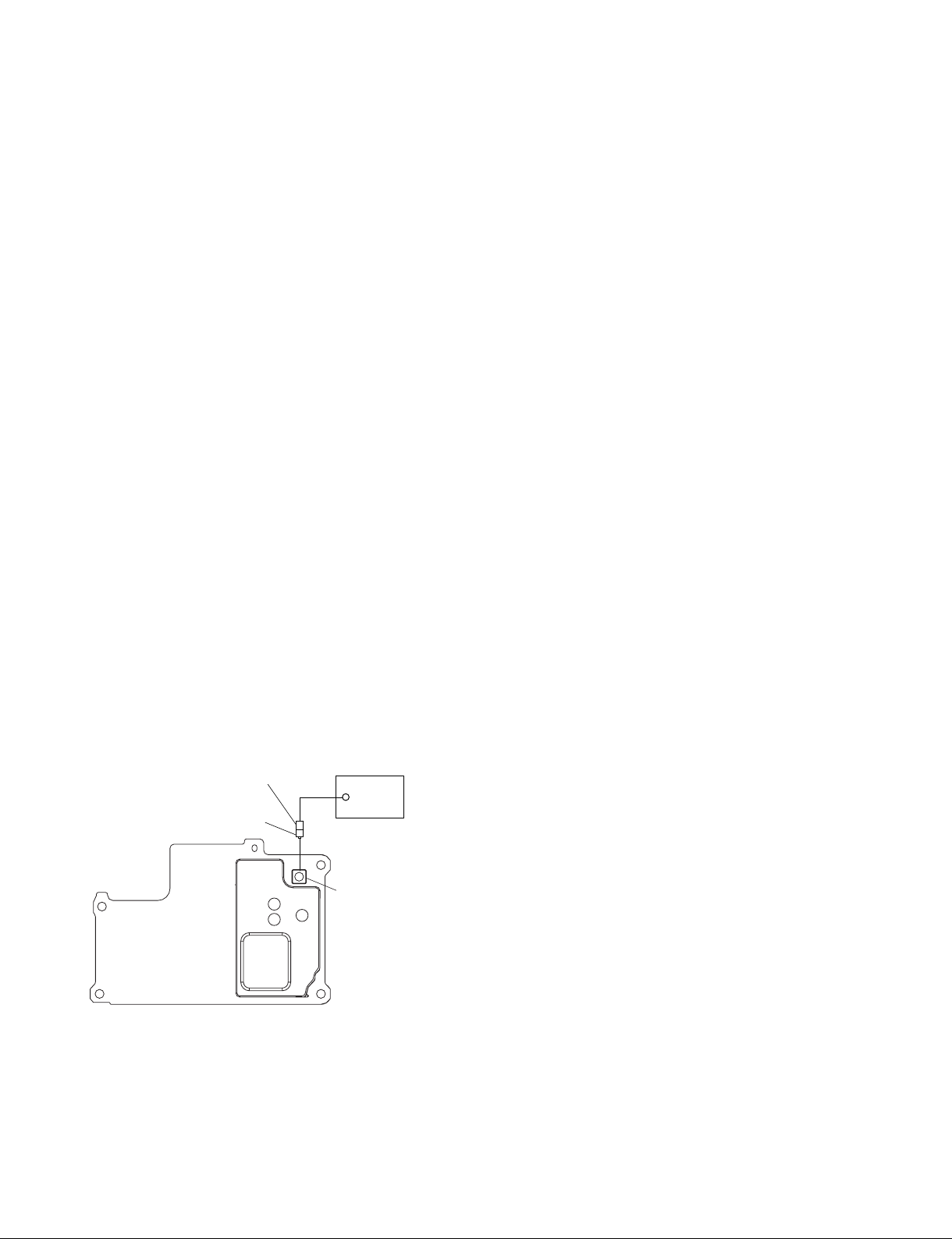
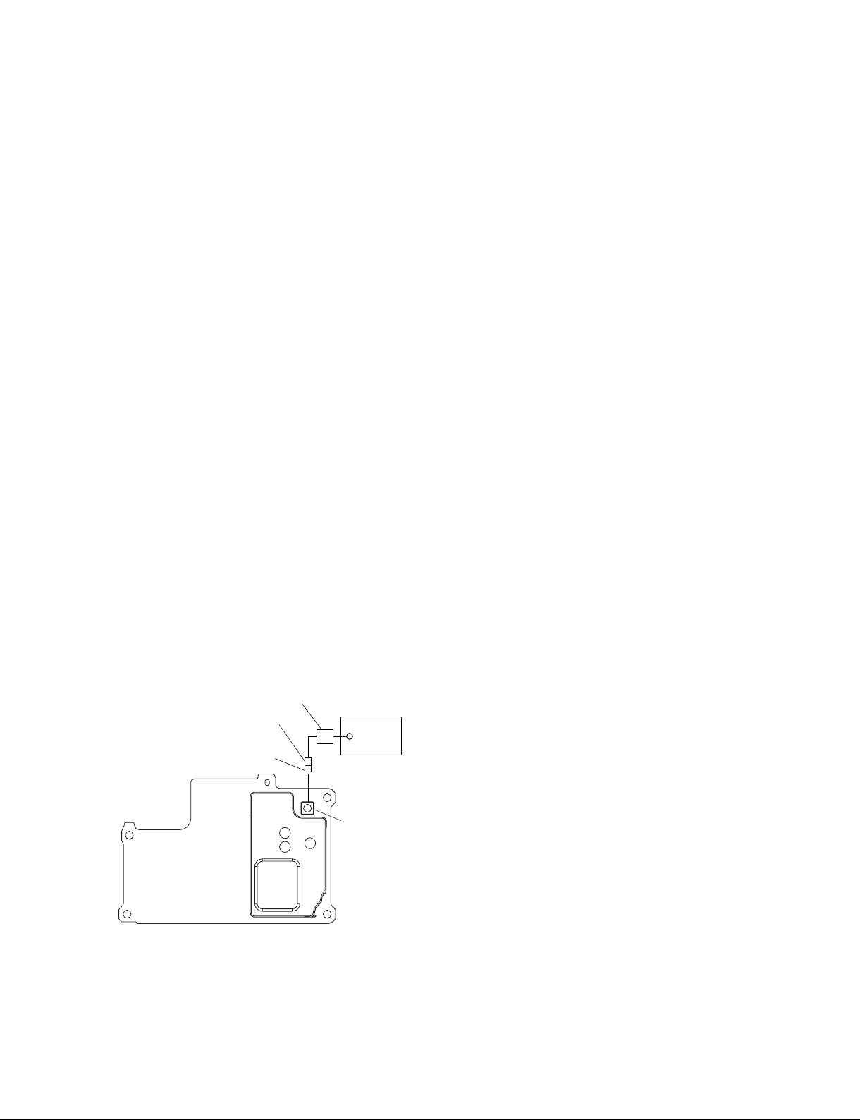
1-4. URX-P2
1-4-1. Disassembly
Rear cabinet Antenna/RF-130 board
M2 x 10
M2 x 10
Antenna
Rear cabinet (RX)
Battery case assembly
Stereo miniature jack CPU-421 board
RF-130 board
CN1
CN2
Stereo
miniature jack
UWP Series
Supplied washer
Supplied nut
P2 x 5
Stereo
miniature jack
Harness
CN1001
CPU-421 board
P2 x 5
Power supply
protection sheet
Do not drop or
lose this
Battery spring
plate
P2 x 5
Set button
1-11

1-4-2. Precaution for Reassembling
When reassembling the UTX-P2, arrange the battery harnesses as shown in the following figures.
Battery spring
(Black)
(Red)
Harness
Battery spring plate
Arranging the harnesses as shown in the figures.
Tape for insulation
Front side Rear side
Front
cabinet
Note
When reassembling the UTX-B2, be careful that
the harness must not be pinched.
1-12
UWP Series

1-4-3. Precaution When Replacing EEPROM (IC11)
When the EEPROM (IC11) is replaced with the new EEPROM, the same data that have been stored in the
removed EEPROM must be written into the newly mounted EEPROM.
1-4-4. Error Messages
When an error occurs, any of the following error messages can be generated by the self-diagnostics
function that is built-in the URX-P2 and can appear on the display section.
Message
Err01
Err02
Err03
NOTONE
Sq OFF
INIT
Error contents
An error occurs in EEPROM data.
The PLL synthesizer circuit does not
lock.
Power supply voltage has exceeded
the range of allowable limits.
The tone signal does not exist, or
any tone signal radio wave other
than 32 kHz is received and the
audio signal is muted.
If you turn on the power while
pressing the “-“ button, the squelch
function release mode is set.
The message is displayed when the
power is turned on while the “SET”
button and the “_“ button are
pressed at the same time.
If the “SET” button and the “_“
button are pressed at the same time,
the UTX-P2 enters the default
setting mode.
Remedial measure
With “Error1” displayed, press and hold the “-“ button for 20 seconds to
read the backup data.The data is successfully read when “RELOAD” is
displayed. If the data fails to be read, check the peripheral circuits of
IC671, and perform the following measures.
. Write the frequency data that corresponds to the desired destination
location, into EEPROM.
. Perform the RF squelch adjustment and the RF level indicator
adjustment. (Refer to Section 2-4.)
If the frequency data that does not corresponds to the desired reception
frequency range is written:
Write the correct frequency data into the EEPROM.
If the error message is displayed even though the frequency data is
correct:
Check the PLL synthesizer circuit (IC321, X301, Q341 and Q342 and its
peripheral circuits on the RF-130 board).
Use the equipment with the power supply of the specified voltage range.
An interference radio wave has occurred in the frequency band in use.
. If an error is displayed while the power of the transmitter is on:
Turn off the power of the transmitter.
. If the RF level indicator of the receiver LCD lights
of the transmitter is turned off:
Set the frequency of the transmit/receive channel that is free from
the interference radio wave.
When the error is not caused by the signal interference, the tone squelch
circuit of receiver or transmitter (both receiver and transmitter) is defective.
. Check the receiver :
. Check the transmitter : Refer to the Service Manual of transmitter.
Turn off the power once and then back on without pressing any button.
Do not press the “SET” button and the “_“ button.
Check the tone squelch. (Refer to Section 2-4.)
If the tone squelch does not work well, check
the tone squelch circuit (IC441 and its
peripheral circuit on the CPU-421 board.)
even when the power
UWP Series
1-13
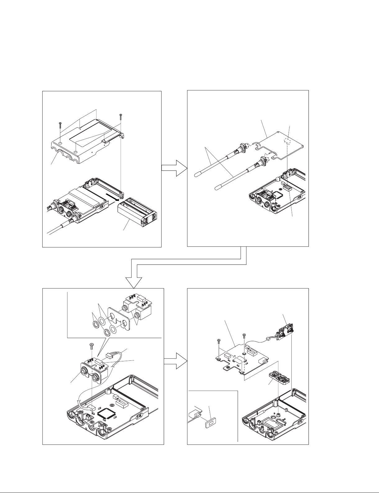
1-5. UTX-P1
1-5-1. Disassembly
Upper sub assembly
Four screws
P2 x 6
Four screws
P2 x 6
Battery
case
Upper sub assembly
Notch
Battery case
Press and hold the notch, and pull up the upper sub assembly.
Case
Case
MB-1094 board
Three screws
B2 x 6
*Remove the
solders.
Screw
P1.7 x 6
Three screws
B1.7 x 8
*Remove the
solders.
XLA connector
Coil spring
XLA connector
Connector holder
Screw
K2 x 5
Remove the solder, and disconnect the harness from
the XLA connector terminal.
Two screws
P2 x 6
Two screws
P2 x 6
MB-1094
board
Lower spring
Two screws
P2 x 6
Battery spring (_) L
Screw
P1.7 x 3
Battery spring (+)
Battery spring (_) R
Locking
Battery spring (+)
1-14
UWP Series
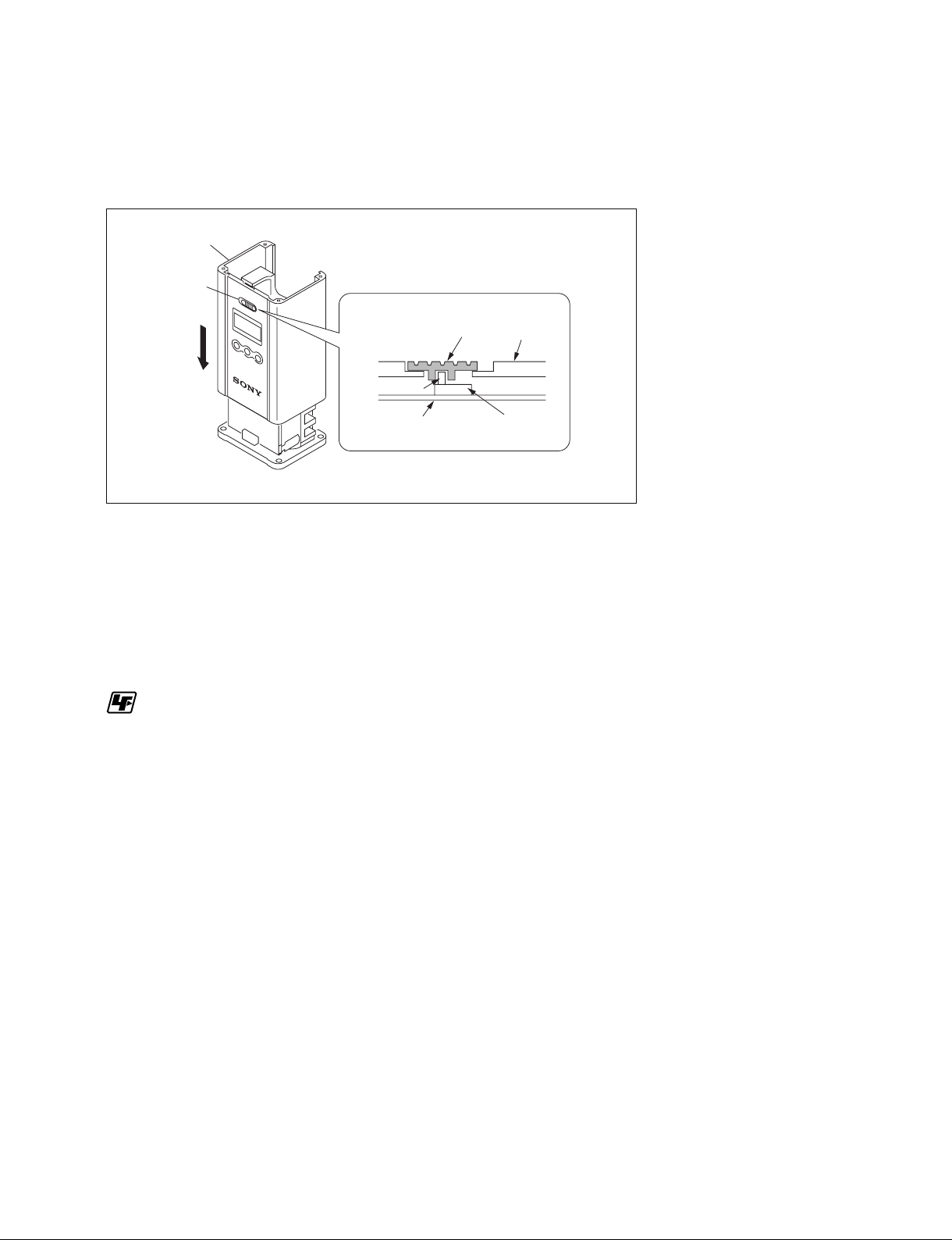
1-5-2. Precaution for Reassembling
When reassembling the UTX-P1, be sure that the knob on the case and the switch on the MB-1094 board
fit together correctly.
Case
Knob
Knob
Lever
MB-1094 board
1-6. Unleaded Solder
Boards requiring use of unleaded solder are printed with a
lead free mark (LF) indicating the solder contains no lead.
(Caution: Some printed circuit boards may not come
printed with the lead free mark due to their particular size.)
: LEAD FREE MARK
m
. Be sure to use the unleaded solder for the printed circuit
board printed with the lead free mark.
. The unleaded solder melts at a temperature about 40 dC
higher than the ordinary solder, therefore, it is recommended to use the soldering iron having a temperature
regulator.
. The ordinary soldering iron can be used but the iron tip
has to be applied to the solder joint for a slightly longer
time. The printed pattern (copper foil) may peel away if
the heated tip is applied for too long, so be careful.
Panel
Switch
UWP Series
1-15

Section 2
Electrical Alignment
2-1. UTX-B2
2-1-1. Equipment and Tools
Equipment Required
Name Specifications Model Name
DC POWER SUPPLY Output regulated voltage : 0 to 5 V, 2 A –
DC AMMETER Measurement : 300 mA –
SPECTRUM ANALYZER Frequency : 10 kHz to 3 GHz ADVANTEST R3361B or equivalent
MODULATION ANALYZER RF input Frequency : 150 kHz to 3 GHz ANRITSU MS616A or equivalent
RF POWER METER Range : 3 uW to 100 mW HP 435B (Power sensor HP 8482A) or equivalent
WITH POWER SENSOR
AUDIO ANALYZER . Oscillator : 20 Hz to 100 kHz HP 8903B (with A-weight filter) or equivalent
FREQUENCY COUNTER Frequency : 10 Hz to 1000 MHz HP 5358A or equivalent
OSCILLOSCOPE Frequency : DC to 10 MHz –
DIGITAL VOLT METER Effective digits : 3 1/2 digits –
. DISTORTION ANALYZER
. S/N METER
. LEVEL METER
Effective digits: 10 digits
Tool
Name Part No. Remarks
MM-SMA conversion connector J-6402-490-A For RF signal output
SMA-BNC conversion connector J-6402-480-A For RF signal output
Adjustor (0.4 x 1.3 mm) 7-721-052-81 Screwdriver for adjustment
UWP Series
2-1
2-1-2. Adjustments
This section describes adjustments and checks which must be
completed to assure that the specifications are complied with.
Make adjustment and checks following the procedure below:
1. Power Supply Voltage Check
↓
2. Carrier Frequency Adjustment
↓
3. RF Power Output Adjustment
↓
4. Reference Frequency Deviation Adjustment
↓
5. Maximum Frequency Deviation Adjustment
↓
6. Distortion Ratio Check
↓
7. S/N Check
↓
8. Frequency Characteristics Check
9. Tone Signal Adjustment
10. Spurious Emissions Check
11. Occupied Band Width Check
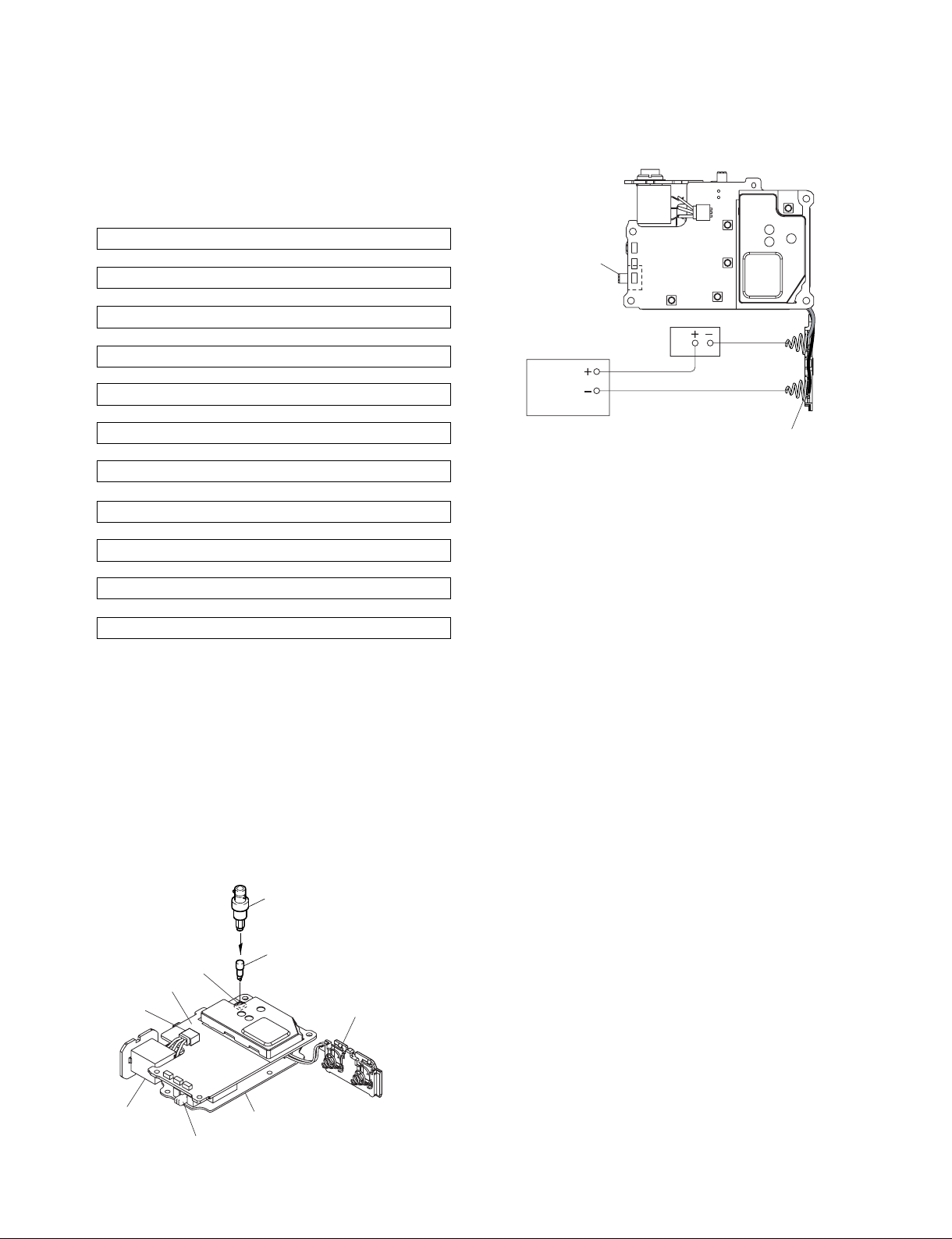
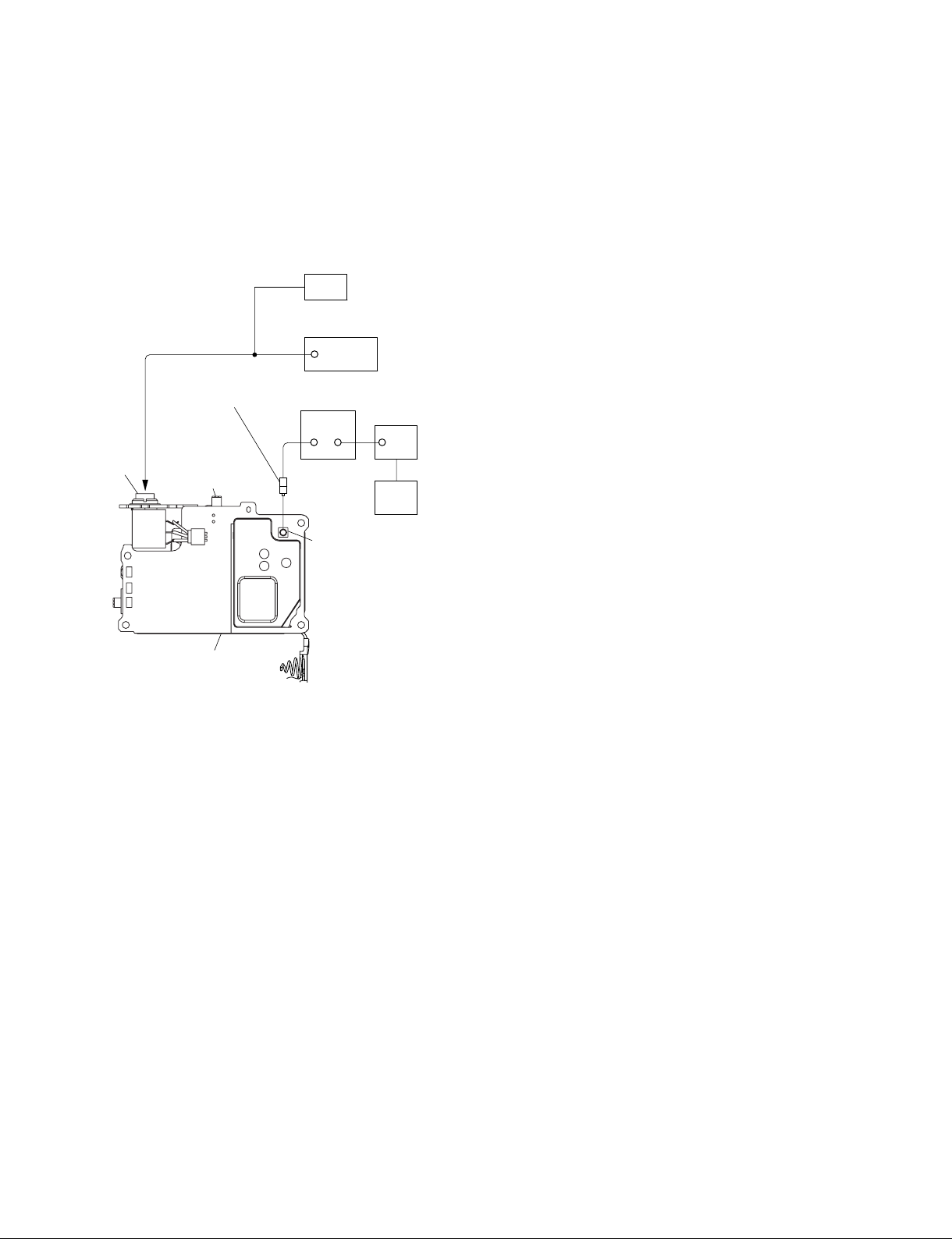
Preparation
1. Perform this adjustment after removing the front/rear
cabinets and battery case from the UTX-B2 unit, and
with the RF-131 board, battery terminal, and LINE/
MIC connector connected to the CPU-422 board.
(Refer to the Section 1-1-1. for removal.)
2. Connect the SMA-BNC conversion connector (J-6402480-A) and the MM-SMA conversion connector (J6402-490-A) to the antenna terminal (CN301) on the
RF-131 board as shown below.
↓
↓
↓
3. Connecting the DC power supply
Supply the DC power to the battery terminal as below.
POWER
switch
(S11/CPU-422 board)
DC ammeter
DC regulated power supply
(DC output voltage : + 3.0 ±0.1 V)
Battery terminal
Check
After the DC power supply connection is complete, set
the power switch (S11/CPU-422 board) to ON, and
check the level on DC ammeter.
DC ammeter indication level: 130 to 200 mA
Switch and Control Initial Setting
Switch and Control Setting
U30 model ; 30-01 channel (566.125 MHz)
U42 model ; 42-01 channel (638.125 MHz)
CE62 model ; Group 00, 62-01 channel (798.125 MHz)
CE67 model ; Group 00, 67-01 channel (838.125 MHz)
KR model ; 59-01 channel (740.125 MHz)
Attenuation setting : 0 dB
Accumulated time setting : “00 : 00”
n
Note down the setting position before the adjustment.
After the Adjustment complete, set the original position.
Red
+
Black
_
RF-131 board
CN401
MIC / LINE
input connector
2-2
SMA-BNC conversion connector
MM-SMA conversion connector
CN301
Battery terminal
CPU-422 board
POWER switch (S11)
UWP Series
Adjustment Location
LCD
CT621
Connections
(For connecting the DC power supply, refer to step
“3. Connecting the DC power supply” in Section 2-1-2.)
GND
C24 (+)
S673
S672_S671
RV521
(Reference frequency
deviation adjustment)
RV441
(AF limiter adjustment)
SET
CN401
+
CN301
RV491
(AF clipper adjustment)
RV511
(Tone signal level adjustment)
1. Power Supply Voltage Check
CPU-422 board
(B side)
RV351
(RF output "H"
adjustment)
CT361
(Output efficiency
optimization)
RV341
(RF output "L"
adjustment)
RF-131 board
(A side)
L12
GND
CPU-422 board (B side)
DC voltmeter
GND
S11
Procedure
1.
Set the POWER switch (S11/CPU-422 board) to ON.
2. Check the DC Voltage of the + terminal on the
CPU-422 board
Specification :
to the specified voltage as below :
C24 (
+ terminal) DC Voltage = +3.3
± 0.1Vdc
3. Check the DC voltage of the
L12/CPU-422 board
specified voltage as below :
Specification :
L12 terminal DC voltage = +5.0 ±0.1Vdc
C24/
to the
Equipment and Tools
. DC power supply
DC output voltage : +3.0 ±0.1 Vdc
. DC ammeter
. Digital volt meter (or Digital multimeter)
Switch and Control Setting
CPU-422 board
Transmission channel
U30 model ; 30-01 channel (566.125 MHz)
U42 model ; 42-01 channel (638.125 MHz)
CE62 model ; Group 00, 62-01 channel (798.125 MHz)
CE67 model ; Group 00, 67-01 channel (838.125 MHz)
KR model ; 59-01 channel (740.125 MHz)
Attenuation setting : 0 dB
Accumulated time setting :“00 : 00”
n
Take note of the settings before starting the confirmation
work.
After confirmation is completed, return the settings to
the original setting before change.
UWP Series
2-3
2. Carrier Frequency Adjustment
Equipment and Tools
. DC power supply
DC output voltage : +3.0 ±0.1 Vdc
. DC ammeter
. Frequency counter
. Adjustor (SONY Part No. 7-721-052-81)
. MM-SMA conversion connector
(SONY Part No. J-6402-490-A)
.
SMA-BNC
(SONY Part No. J-6402-480-A)
Switch and Control Setting
Transmission channel
U30 model ; 32-01 channel (578.125 MHz)
U42 model ; 42-01 channel (650.125 MHz)
CE62 model ; Group 00, 63-32 channel (810.000 MHz)
CE67 model ; Group 00, 68-32 channel (850.000 MHz)
KR model ; 60-01 channel (746.125 MHz)
Attenuation setting : 0 dB
Accumulated time setting :“00 : 00”
n
Note down the setting position before the adjustment.
After the Adjustment complete, set the original position.
conversion
connector
Procedure
1. Connect a frequency counter to the antenna terminal
(CN301/RF-131 board) via the MM-SMA conversion
connector and the SMA-BNC conversion connector.
2. Adjust 1CT621 so that the frequency counter reading
meets the following specification.
Specification : Carrier frequency mentioned below.
U30 model ; 578.125 MHz ±1 kHz
U42 model ; 650.125 MHz ±1 kHz
CE62 model ; 810.000 MHz ± 1 kHz
CE67 model ; 850.000 MHz ± 1 kHz
KR model ; 746.125 MHz ± 1 kHz
Adjustment : 1CT621/CPU-422 board (B side)
(Refer to page 2-3 for the adjustment location.)
Connections
(For connecting the DC power supply, refer to step
“3. Connecting the DC power supply” in Section 2-1-2.)
Frequency counter
SMA-BNC conversion connector
MM-SMA conversion connector
CN301
RF-131 board
(A side)
2-4
UWP Series
3. RF Power Output Adjustment
Equipment and Tools
. DC power supply
DC output voltage : +3.0 ±0.1 Vdc
. DC ammeter
. Power meter (with power sensor)
. Adjustor (SONY Part No. 7-721-052-81)
. MM-SMA conversion connector
(SONY Part No. J-6402-490-A)
.
SMA-BNC
(SONY Part No. J-6402-480-A)
Switch and Control Setting
Transmission channel
U30 model ; 32-01 channel (578.125 MHz)
U42 model ; 42-01 channel (650.125 MHz)
CE62 model ; Group 00, 63-32 channel (810.000 MHz)
CE67 model ; Group 00, 68-32 channel (850.000 MHz)
KR model ; 60-01 channel (746.125 MHz)
Attenuation setting : 0 dB
Accumulated time setting :“00 : 00”
RF power output : “H”
n
Note down the setting position before the adjustment.
After the Adjustment complete, set the original position.
Connections
(For connecting the DC power supply, refer to step
“3. Connecting the DC power supply” in Section 2-1-2.)
conversion
connector
Procedure
1. Connect the power meter (with power sensor) to the antenna terminal (CN301/RF-131 board) via the MMSMA conversion connector and the
sion
connector
.
SMA-BNC
conver-
2. Adjust 1CT361 so that the power meter reading meets
the following specification.
Specification : power meter = Maximum
Adjustment : 1CT361/RF-131 board (A side)
(Refer to page 2-3 for the adjustment location.)
3. Adjust 1RV351 so that the power meter reading meets
the following specification.
Specification :
. U30, U42, CE62 and CE67 models :
Power meter = 28 ± 1 mW
. KR model :
Power meter = 9 mW
+0.5
_0.1
Adjustment : 1RV351/RF-131 board (A side)
(Refer to page 2-3 for the adjustment location.)
4. Set the transmission output to “L”.
5. Adjust 1RV341 so that the power meter reading meets
the following specification.
Specification :
. U30, U42, CE62 and CE67 models :
Power meter = 5 mW ±2 mW
. KR model :
Power meter = 1.6 ± 0.6 mW
Adjustment : 1RV341/RF-131 board (A side)
(Refer to page 2-3 for the adjustment location.)
SMA-BNC conversion connector
MM-SMA conversion connector
UWP Series
Power sensor
Power meter
CN301
RF-131 board
(A side)
2-5

4. Reference Frequency Deviation
Adjustment
Equipment and Tools
. DC power supply
DC output voltage : +3.0 ±0.1Vdc
. DC ammeter
. Audio analyzer
. Modulation analyzer
MEASUREMENT : FM
MEASUREMENT RANGE : AUTO or ± 10 kHz
HPF : 50 Hz
LPF : 20 kHz or 15 kHz
DE EMPHASIS : 50 usec
. Adjustor (SONY part No. 7-721-052-81)
. MM-SMA conversion connector
(SONY Part No. J-6402-490-A)
.
SMA-BNC
(SONY Part No. J-6402-480-A)
Switch and Control Setting
Transmission channel
U30 model ; 32-01 channel (578.125 MHz)
U42 model ; 42-01 channel (650.125 MHz)
CE62 model ; Group 00, 63-32 channel (810.000 MHz)
CE67 model ; Group 00, 68-32 channel (850.000 MHz)
KR model ; 60-01 channel (746.125 MHz)
MIC/LINE change switch
(S401/RF-131 board) : MIC
Attenuation setting : 0 dB
Accumulated time setting :“00 : 00”
n
Note down the setting position before the adjustment.
After the Adjustment complete, set the original position.
conversion
connector
Connections
(For connecting the DC power supply, refer to step
“3. Connecting the DC power supply” in Section 2-1-2.)
Level meter
Audio analyzer
MM-SMA conversion connector and
SMA-BNC conversion connector
AF input
connector
MIC / LINE
change switch
(S401 / RF-131 board)
RF-131 board
analyzer
OscilloscopeModulation
CN301
Procedure
1. Input 1 kHz, _ 60 dBV (_57.8 dBm) signal to the AF
INPUT connector.
(0 dBV = 1 Vrms)
2. Connect a modulation analyzer to the antenna terminal
(CN301/RF-131 board) via the MM-SMA conversion
connector and the
SMA-BNC
conversion
connector
.
3. Adjust 1RV521 so that the frequency deviation for the
modulation analyzer reading meets the following specification.
Specification :
Frequency deviation = ±7 kHz ±0.1 kHz
Adjustment : 1RV521/RF-131 board (A side)
(Refer to page 2-3 for the adjustment location.)
2-6
UWP Series

5. Maximum Frequency Deviation
Adjustment
Equipment and Tools
. DC power supply
DC output voltage : +3.0 ±0.1Vdc
. DC ammeter
. Audio analyzer
. Modulation analyzer
MEASUREMENT : FM
MEASUREMENT RANGE : AUTO or ± 100 kHz
HPF : 50 Hz
LPF : 15 kHz or 20 kHz
DE EMPHASIS : 50 usec
. Oscilloscope
. Adjustor (SONY part No. 7-721-052-81)
. MM-SMA conversion connector
(SONY Part No. J-6402-490-A)
.
SMA-BNC
(SONY Part No. J-6402-480-A)
Switch and Control Setting
Transmission channel
U30 model ; 32-01 channel (578.125 MHz)
U42 model ; 42-01 channel (650.125 MHz)
CE62 model ; Group 00, 63-32 channel (810.000 MHz)
CE67 model ; Group 00, 68-32 channel (850.000 MHz)
KR model ; 60-01 channel (746.125 MHz)
MIC/LINE change switch
(S401/RF-131 board) : MIC
Attenuation setting : 0 dB
Accumulated time setting :“00 : 00”
n
Note down the setting position before the adjustment.
After the Adjustment complete, set the original position.
Connections
. Same as “4. Reference Frequency Division adjustments”.
. For connecting the DC power supply, refer to step
“3. Connecting the DC power supply” in Section 2-1-2.
Procedure
1.
Input 1 kHz, _20 dBV (_17.8 dBm) signal to the AF INPUT connector (with Mic input cable). (0 dBV = 1 Vrms)
2. Adjust 1RV441/RF-131 so that the frequency devia-
tion for the modulation analyzer reading meets the following specification.
Specification : Frequency deviation = ±34.5 kHz ± 0.5 kHz
Adjustment :
3.
Input 1 kHz, _10 dBV (_7.8 dBm) signal to the AF INPUT connector (with Mic input cable). (0 dBV = 1 Vrms)
conversion
connector
1RV441/RF-131 board (A side)
4. Connect a modulation analyzer to the antenna terminal
(CN301/RF-131 board) via the MM-SMA conversion
connector and the
5.
Adjust 1RV491
SMA-BNC
/RF-131
conversion
connector
.
so that the frequency deviation
for the modulation analyzer reading meets the following
specification.
Specification :
Frequency deviation = ± 39.5 kHz ± 0.5 kHz
Adjustment : 1RV491/RF-131 board (A side)
6. Distortion Ratio Check
Equipment and Tools
. DC power supply
DC output voltage : +3.0 ±0.1Vdc
. DC current meter
. Audio analyzer
. Modulation analyzer
MEASUREMENT : FM
MEASUREMENT RANGE : AUTO or ± 40 kHz
HPF : 50 Hz
LPF : 15 kHz or 20 kHz
DE EMPHASIS : 50 usec
. Oscilloscope
. MM-SMA conversion connector
(SONY Part No. J-6402-490-A)
.
SMA-BNC
(SONY Part No. J-6402-480-A)
Switch and Control Setting
Transmission channel
U30 model ; 32-01 channel (578.125 MHz)
U42 model ; 42-01 channel (650.125 MHz)
CE62 model ; Group 00, 63-32 channel (810.000 MHz)
CE67 model ; Group 00, 68-32 channel (850.000 MHz)
KR model ; 60-01 channel (746.125 MHz)
MIC/LINE change switch
(S401/RF-131 board) : MIC
Attenuation setting : 0 dB
Accumulated time setting :“00 : 00”
n
Take note of the settings before starting the confirmation
work.
After confirmation is completed, return the settings to
the original setting before change.
conversion
connector
UWP Series
2-7
Connections
. For connecting the DC power supply, refer to step
“3. Connecting the DC power supply” in Section 2-1-2.
. For the connection to the AF IN connector (CN1), refer
to the section “4. Reference Frequency Deviation
Adjustment”.
Level meter
Audio analyzer
Oscillator
MM-SMA conversion connector and
AF input
connector
SMA-BNC conversion connector
RFINAF
MIC / LINE
change switch
(S401 / RF-131 board)
RF-131 board
Modulation
analyzer
CN301
Distortion
analyzer
OUT
Oscilloscope
Procedure
1. Connect the audio analyzer (distortion analyzer) to the
AF OUT connector for the modulation analyzer.
2. Set the audio analyzer to distortion measurement
(DISTORTION mode).
3. Input 1 kHz, _60 dBV (_57.8 dBm) signal to the AF
INPUT connector from audio analyzer (oscillator).
(0 dBV = 1 Vrms)
4. Check that the distortion analyzer reading is less than
1.0%.
5. Input 1 kHz, _23 dBV (_20.8 dBm) signal to the AF
INPUT connector.
6. Check that the distortion analyzer reading is less than
1.0%.
2-8
7. S/N Check
Equipment and Tools
. DC power supply
DC output voltage : +3.0 ± 0.1Vdc
. DC ammeter
. Audio analyzer
. Modulation analyzer
MEASUREMENT : FM
MEASUREMENT RANGE : ± 40 kHz
HPF : 50 Hz
LPF : 15 kHz or 20 kHz
DE EMPHASIS : 50 usec
. Oscilloscope
. MM-SMA conversion connector
(SONY Part No. J-6402-490-A)
.
SMA-BNC
(SONY Part No. J-6402-480-A)
Switch and Control Setting
Transmission channel
U30 model ; 32-01 channel (578.125 MHz)
U42 model ; 42-01 channel (650.125 MHz)
CE62 model ; Group 00, 63-32 channel (810.000 MHz)
CE67 model ; Group 00, 68-32 channel (850.000 MHz)
KR model ; 60-01 channel (746.125 MHz)
MIC/LINE change switch
(S401/RF-131 board) : MIC
Attenuation setting : 0 dB
Accumulated time setting :“00 : 00”
n
Take note of the settings before starting the confirmation
work.
After confirmation is completed, return the settings to
the original setting before change.
Connections
. Same as “6. Distortion Ratio Check”.
. For connecting the DC power supply, refer to step
“3. Connecting the DC power supply” in Section 2-1-2.
Procedure
1. Connect the audio analyzer (level meter) to the AF OUT
connector for the modulation analyzer.
2. Set the modulation analyzer.
3. Input 1 kHz, _ 60 dBV (_57.8 dBm) signal to the AF
INPUT connector from audio analyzer (oscillator).
(0 dBV = 1 Vrms)
4. Set the audio analyzer to S/N measurement (with Aweighting filter).
5. Check that the S/N reading is more than 30 dB.
n
Perform the checking with the AF INPUT connector
short-circuit.
conversion
connector
UWP Series

8. Frequency Characteristics Check
Equipment and Tools
. DC power supply
DC output voltage : +3.0 ±0.1Vdc
. DC ammeter
. Audio analyzer
. Modulation analyzer
MEASUREMENT : FM
MEASUREMENT RANGE : ±40 kHz
HPF : 50 Hz
LPF : 15 kHz or 20 kHz
DE EMPHASIS : 50 usec
. Oscilloscope
. MM-SMA conversion connector
(SONY Part No. J-6402-490-A)
.
SMA-BNC
(SONY Part No. J-6402-480-A)
Switch and Control Setting
Transmission channel
U30 model ; 32-01 channel (578.125 MHz)
U42 model ; 42-01 channel (650.125 MHz)
CE62 model ; Group 00, 63-32 channel (810.000 MHz)
CE67 model ; Group 00, 68-32 channel (850.000 MHz)
KR model ; 60-01 channel (746.125 MHz)
MIC/LINE change switch
(S401/RF-131 board) : MIC
Attenuation setting : 0 dB
Accumulated time setting :“00 : 00”
n
Take note of the settings before starting the confirmation
work.
After confirmation is completed, return the settings to
the original setting before change.
Connections
. Same as “6. Distortion Ratio Check”.
. For connecting the DC power supply, refer to step
“3. Connecting the DC power supply” in Section 2-1-2.
conversion
connector
6.
Set the SENSITIVITY on the audio analyzer (level
meter) so that the audio analyzer (level meter) reads 0 dB.
7. Switch the oscillation frequency for the audio analyzer
(oscillator) from 1 kHz to 100 Hz.
8. Check that audio analyzer (level meter) reading is _1
± 2 dB.
9. Switch the oscillation frequency for the audio analyzer
(oscillator) from 100 Hz to 15 kHz.
10. Check that the reading for the audio analyzer (level
meter) is +3 ± 2 dB.
9. Tone Signal Adjustment
Equipment and Tools
. DC power supply
DC output voltage : +3.0 ±0.1Vdc
. DC current meter
. Frequency counter
. Spectrum analyzer
. Modulation analyzer
. RF adjusting cable (SONY part No. 7-721-052-81)
. MM-SMA conversion connector
(SONY Part No. J-6402-490-A)
.
SMA-BNC
(SONY Part No. J-6402-480-A)
Switch and Control Setting
Transmission channel
U30 model ; 32-01 channel (578.125 MHz)
U42 model ; 42-01 channel (650.125 MHz)
CE62 model ; Group 00, 63-32 channel (810.000 MHz)
CE67 model ; Group 00, 68-32 channel (850.000 MHz)
KR model ; 60-01 channel (746.125 MHz)
Attenuation setting : 0 dB
Accumulated time setting :“00 : 00”
n
Note down the setting position before the adjustment.
After the Adjustment complete, set the original position.
conversion
connector
Procedure
1. Connect the audio analyzer (level meter) to the AFOUT connector for the modulation analyzer.
2. Set the modulation analyzer.
3. Set the audio analyzer to level meter mode.
4. Input 1 kHz, _60 dBV (_57.8 dBm) signal to the AF
INPUT connector from audio analyzer (oscillator).
5.
Check the indication on the audio analyzer (level meter).
UWP Series
2-9
Frequency deviation adjustment
Frequency check
Connections
(For connecting the DC power supply, refer to step
“3. Connecting the DC power supply” in Section 2-1-2.)
MM-SMA conversion connector and
SMA-BNC conversion connector
Spectrum analyzer
CN301
RF-131 board
Procedure
1. Connect the spectrum analyzer to the antenna terminal
(CN301/RF-131 board) via the MM-SMA conversion
connector and the
SMA-BNC
conversion
connector
.
2. Set the spectrum analyzer as below:
CENTER FREQUENCY (fc)
U30 model ; 578.125 MHz ± 1 kHz
U42 model ; 650.125 MHz ± 1 kHz
CE62 model ; 810.000 MHz ± 1 kHz
CE67 model ; 850.000 MHz ± 1 kHz
KR model ; 746.125 MHz ± 1 kHz
REFERENCE LEVEL : 20 dBm
FREQUENCY SPAN
: 200kHz (20 kHz/DIV)
RBW (resolution band width) : 3kHz
VBW (video band width) : 1kHz
ATT : 20 dB
3. Adjust 1RV511/RF-131 board (A side) so that level
between carrier frequency (frequency center level) on
spectrum analyzer and tone signal is within 29 dB ±1 dB.
Connections
(For connecting the DC power supply, refer to step
“3. Connecting the DC power supply” in Section 2-1-2.)
Modulation
analyzer
RF
AF
IN
MM-SMA conversion connector and
SMA-BNC conversion connector
RF-131 board
OUT
CN301
Frequency
counter
Procedure
n
Perform the checking with the AF INPUT connector shortcircuit.
1. Set the modulation analyzer as below:
MEASUREMENT : FM
MEASUREMENT RANGE : ± 40 kHz
HPF : 4 kHz
LPF : >20 kHz
DE EMPHASIS : OFF
2. Check that the frequency counter (resolution : 0.1 Hz
setting) reading is 32.000 kHz ± 1Hz.
2-10
20 dBm
29±1 dB
v:10 dB/div
H:20 MHz/div
fc
32.000 kHz
UWP Series
 Loading...