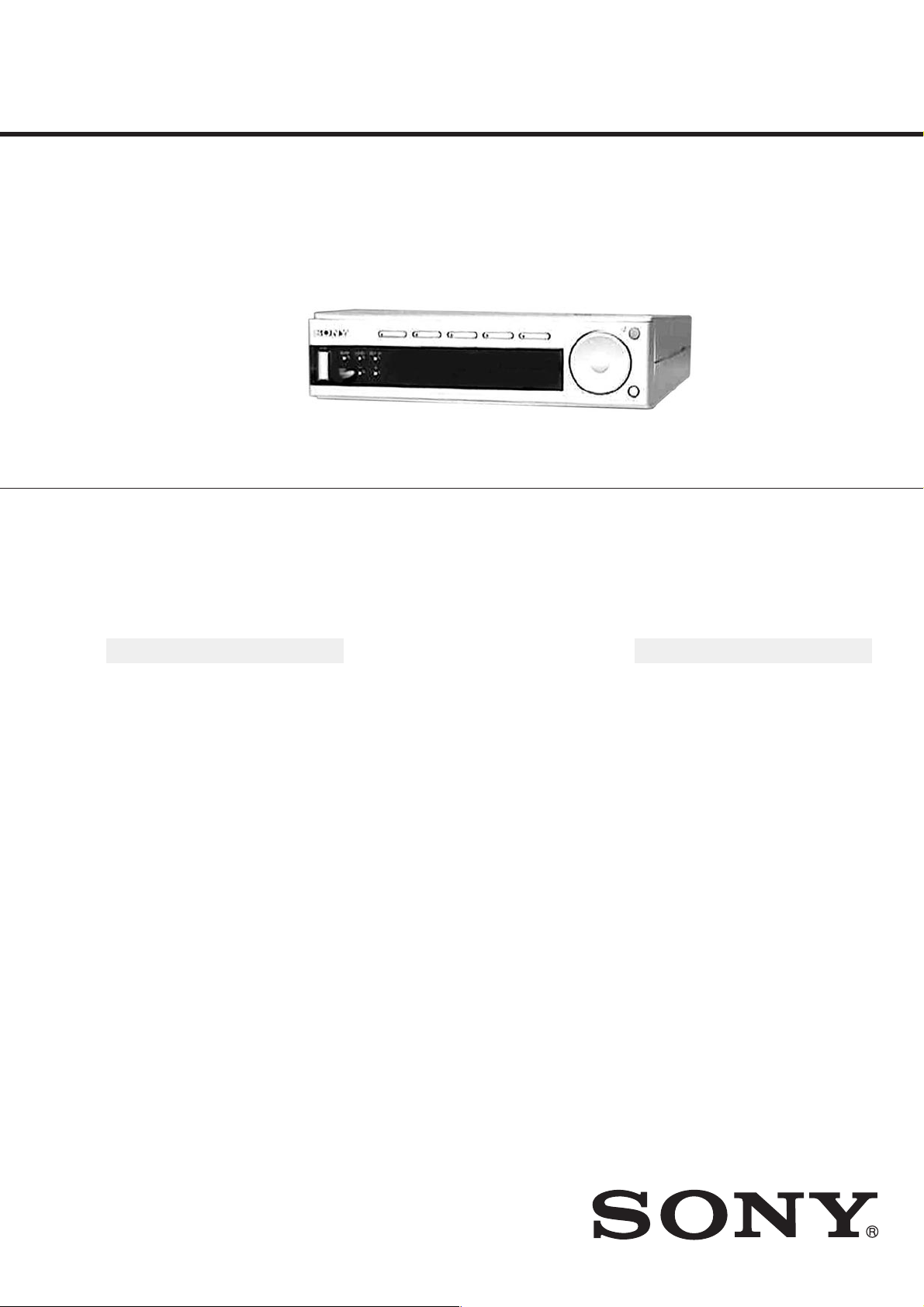
Sony TAVE-215 Service manual
http://cxema.ru
TA-VE215
SERVICE MANUAL
• This set is the Amplifier section in
HT-K215.
This amplifier incorporates Dolby* Digital and Pro Logic
Surround and the DTS** Digital Surround System.
Manufactured under licensefrom Dolby Laboratories.
*
“Dolby”, “AC-3”, “Pro Logic” and the double-D symbol a are
trademarks of Dolby Laboratories.
SPECIFICATIONS
AEP Model
UK Model
E Model
Australian Model
Chinese Model
Amplifier section
POWER OUTPUT
Rated Power Output at Stereo mode
(8 ohms 1 kHz, THD
0.7%)
25W+25W
Reference Power Output
(8 ohms 1 kHz, THD
0.7%)
Front: 25W+25W
Center: 25 W
Rear: 25W+25W
Frequency response
DVD, TV, VIDEO, AUX:
20 Hz - 20 kHz + 0.5/
–2 dB
Inputs (Analog)
5.1CH/SAT,TV, VIDEO:
Sensitivity: 250 mV
Impedance: 50
kilohms
a)
: 96 dB (A, 250
S/N
b)
)
mV
Inputs (Digital)
DVD, AUX (optical):
Sensitivity: –
Impedance: –
S/N: 100 dB (A, 20
kHz LPF)
Outputs SUB WOOFER:
Voltage: 2 V
Impedance: 1
kilohms
General
Power requirements
220-230 V AC, 50/60 Hz
Power consumption
120 W
Dimensions 296.5 215 60 mm
including projecting
parts and controls
Mass (Approx.)
4.2 kg
HOME THEATER SYSTEM

http://cxema.ru
TABLE OF CONTENTS
1. GENERAL ········································································· 3
2. TEST MODE····································································· 4
3. DIAGRAMS········································································ 5
3-1. Circuit Boards Location ·············································· 5
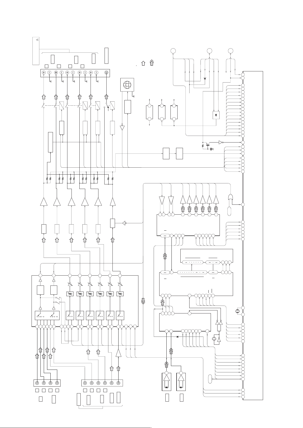
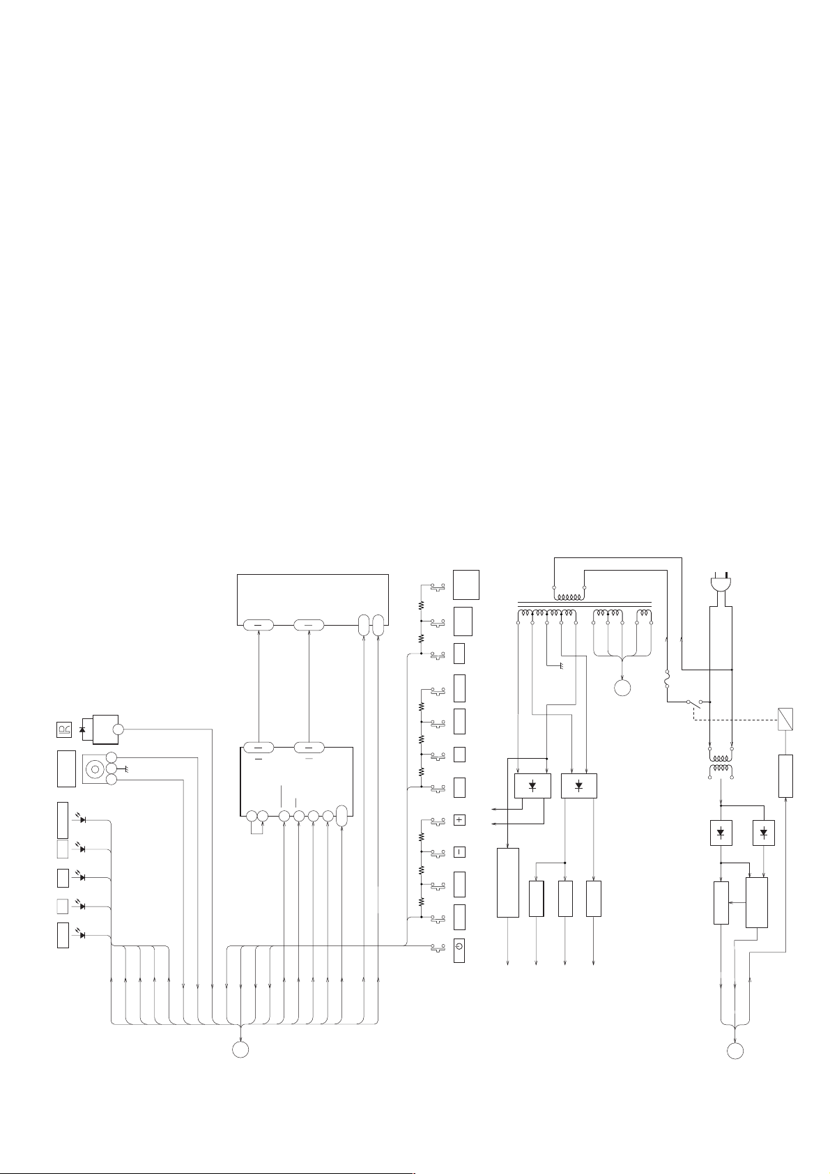
3-2. Block Diagram
– MAIN Section – ······················································· 6
– POWER Section – ···················································· 7
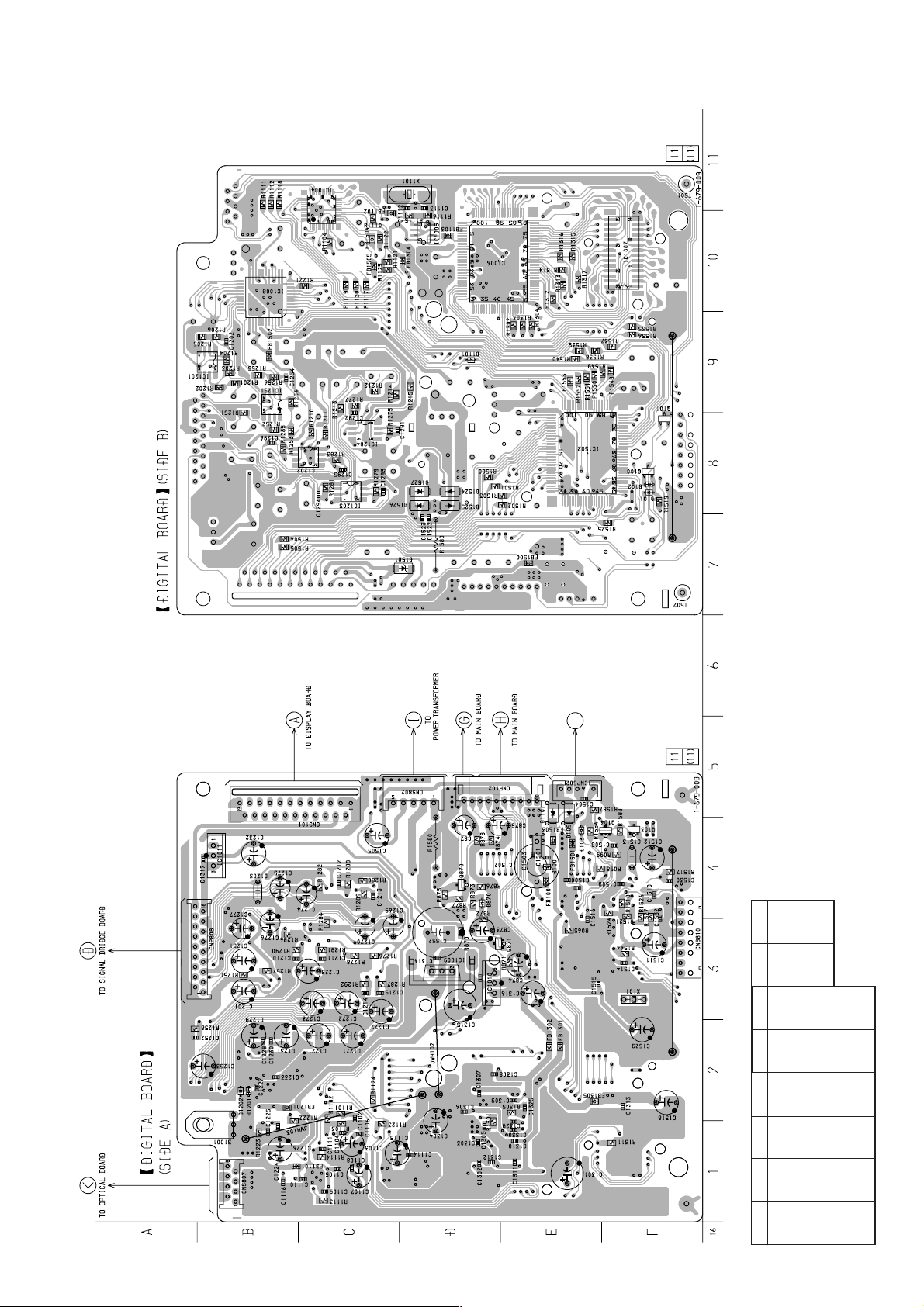
3-3. Printed Wiring Boards – DIGITAL Section – ··········· 8
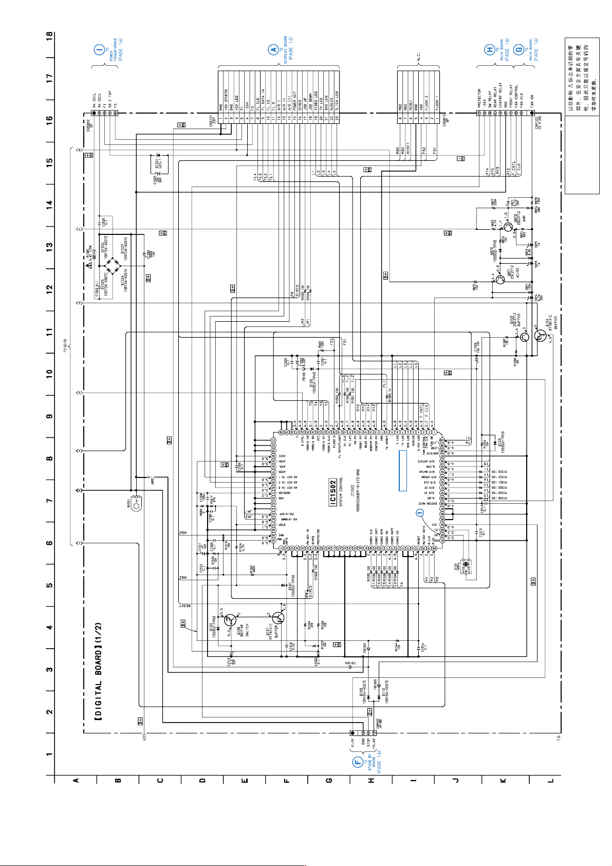
3-4. Schematic Diagram – DIGITAL Section (1/2) –········ 9
3-5. Schematic Diagram – DIGITAL Section (2/2) –······ 10
3-6. Printed Wiring Boards
– OPTICAL / SIGNAL BRIDGE Section –·············11
3-7. Schematic Diagram
– SIGNAL BRIDGE Section –··································11
3-8. Schematic Diagram – DISPLAY Section –·············· 12
3-9. Printed Wiring Boards – DISPLAY Section – ·········· 13
3-10. Printed Wiring Boards – MAIN Section – ··············· 14
3-11. Schematic Diagram – MAIN Section (1/2) – ··········· 15
3-12. Schematic Diagram – MAIN Section (2/2) – ··········· 16
3-13. Printed Wiring Boards – POWER Section – ············ 17
3-14. IC Pin Function Description ······································ 18
3-15. IC Block Diagrams ···················································· 19
4. EXPLODED VIEWS····················································· 20
5. ELECTRICAL PARTS LIST····································· 22
• Grounding connection at the two points between the MAIN
board and the chassis is necessary while the main power
to the MAIN board is turned on.
• Jig is used to inspect the DIGITAL board.
1. Between the DIGIT AL board CNS807 and OPTICAL board CNP807
8 P/L=300 (A-2501-2060A)
2. Between the DIGITAL board CNS808 and SIGNAL BRIDGE
board CNS808
18 P/L=300 (A-2501-207-A)
SAFETY-RELATED COMPONENT WARNING!!
COMPONENTS IDENTIFIED BY MARK 0 OR DOTTED LINE WITH
MARK 0 ON THE SCHEMATIC DIAGRAMS AND IN THE PARTS
LIST ARE CRITICAL TO SAFE OPERATION. REPLACE THESE
COMPONENTS WITH SONY PARTS WHOSE PART NUMBERS
APPEAR AS SHOWN IN THIS MANUAL OR IN SUPPLEMENTS
PUBLISHED BY SONY.
Flexible Circuit Board Repairing
• Keep the temperature of soldering iron around 270˚C
during repairing.
• Do not touch the soldering iron on the same conductor of the
circuit board (within 3 times).
• Be careful not to apply force on the conductor when soldering
or unsoldering.
2
http://cxema.ru
SECTION 1
GENERAL
This section is extracted
from instruction manual.
1
VIDEO TV DVD AUX 5.1CH/SAT
?/1
SURR LEVEL SET UP
+–
45 67
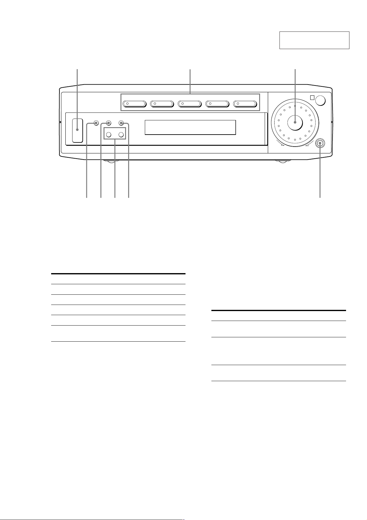
1 ?/1 switch
Press to turn the amplifier on and off.
2 Function buttons
Press one of the buttons to select the component you
want to use.
To select Press
VCR VIDEO
TV TV
DVD player DVD
An audio component AUX
DVD through AC-3 5.1 CH/SAT
decoder
After selecting the component, turn on the component
you selected and play the program source.
• After selecting VCR or DVD player, turn on the TV and set
the TV’s video input to match the component you selected.
23
MASTER VOLUME
R
+
SOUND FIELD MODE
8
5 LEVEL button
Press repeatedly to activate the speaker level
parameters (page 30) and to adjust the various speaker
level parameters (front balance, rear balance, etc.). You
can then make various settings using the +/– buttons
(7).
6 SET UP button
Press repeatedly to activate the setup mode and to
select any of the following indications. You can then
make various settings using the +/– buttons (7).
When you select You can
Speaker type Specify the type of speakers.
Speaker setup Specify the front, center,rear
Speaker Distance Specify the front, center,and rear
(page 15)
speaker sizes, the rear speaker
position, and whether or not you
are using a sub woofer. (page 15)
speaker distances. (page 17)
3 MASTER VOLUME control
After turning on the component you selected, rotate to
adjust the volume.
4 SURR button
Press repeatedly to activate the surround parameters
(page 29) and to adjust the various surround
parameters (effect level, wall type, etc.). You can then
make various settings using the +/– buttons (7).
7 +/– buttons
Press to adjust the selected speaker level and surround
parameters (etc.).
8 SOUND FIELD MODE
Press repeatedly to activate the sound field selection
mode and to select the sound field you want (page 24).
3
http://cxema.ru
SECTION 2
TEST MODE
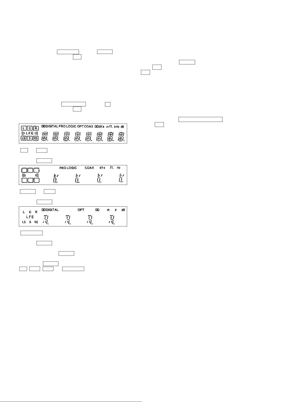
SOFTWARE VERSION DISPLAY MODE
* The software version is displayed.
* Procedure:
While depressing the 5.1CH/SAT and the VIDEO buttons
simultaneously, press the po wer 1/u b utton to turn on the main
power. The destination and the software version are displayed.
FLUORESCENT INDICATOR TUBE TEST MODE
* All fluorescent segments are tested. When this test is activated,
all segments turn on at the same time, then each segment turns on
one after another.
* Procedure:
While depressing the 5.1CH/SAT and the + buttons
simultaneously, press the po wer 1/u b utton to turn on the main
power.
1. All segments turn on.
TV and AUX LED turn on.
2. Press the VIDEO button, confirm display
ALL CLEAR MODE
* All preset contents are cleared when this mode is activated. Use
this mode before returning the product to clients upon completion
of repair.
* Procedure:
While depressing the SET UP button simultaneously, press the
power 1/u button to turn on the main power. Alternatively , pr ess
1/u more than 4S. The message “ALL CLEAR” appears and
initialization is performed.
SURROUND CLEAR MODE
* The preset sound field is cleared when this mode is activated.
Use this mode before returning the product to clients upon
completion of repair.
* Procedure:
While depressing the SOUND FIELD MODE button, press the
power 1/u button to turn on the main power. The message
“SUR CLR” appears and initialization is performed.
VIDEO and DVD LED turn on.
3. Press the VIDEO button, confirm display
5.1CH/SAT LED turn on.
4. Press the VIDEO button, All segments turn off.
5. Every pressing of the VIDEO button turns on each segment
one after another in the same order.
(Not only the VIDEO button, b ut also the other buttons sach as
TV , DVD , AUX and 5.1CH/SAT can be used.)
4
http://cxema.ru
W or less unless otherwise
B
These are omitted.
CE
Q
4
/
1
: internal component.
f
specified.
50 WV or less are not indicated except for electrolytics
and tantalums.
• All resistors are in Ω and
•
Note on Schematic Diagram:
• All capacitors are in µF unless otherwise noted. pF: µµF
The components identified by
• 2 : nonflammable resistor.
• 5 : fusible resistor .
• C : panel designation.
mark 0 or dotted line with mark
0 are critical for safety.
Replace only with part number
specified.
• U : B+ Line.
• V : B– Line.
• H : adjustment for repair.
• Voltages are taken with a VOM (Input impedance 10 M Ω).
Voltage variations may be noted due to normal produc-
tion tolerances.
Voltage variations may be noted due to normal produc-
• Waveforms are taken with a oscilloscope.
tion tolerances.
• Circled numbers refer to waveforms.
F : ANALOG
c : DIGITAL
• Signal path.
• Waveform
5.6 Vp-p
16 MHz
IC1502 is XO
1
NOTE FOR PRINTED WIRING BOARDS AND SCHEMATIC DIAGRAMS
Note on Printed Wiring Board:
: internal component.
f
• b : Pattern from the side which enables seeing.
• X : parts extracted from the component side.
•
DIGITAL board
(Side A) the parts face are indicated.
Caution:
Pattern face side: Parts on the pattern f ace side seen from
(Side B) the pattern face are indicated.
Parts face side: Parts on the parts face side seen from
OPTICAL board
These are omitted.
CE
Q
B
• Indication of transisitor.
These are omitted.
E
C
Q
B
55
SIGNAL BRIDGE board
SECTION 3
DIAGRAMS
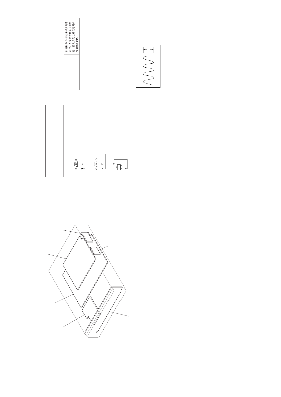
3-1. CIRCUIT BOARDS LOCATION
MAIN board
DISPLAY board
STAND BY board
http://cxema.ru
SPEAKERS
IMPEDANCE USE8-16
TM603
L_CH
14
IC701 POWER AMP.
Q361
MUTE
FRONT
L
R_CH
RY730
Q730
DC DET.RY MUTE
Q722,Q723,Q725
FRONT_RY
14
IC751 POWER AMP.
Q365
MUTE
R
RY DRIVE
IC601 POWER AMP.
REAR
L
SL_CH
SR_CH
RY601
14
IC651 POWER AMP.
Q362
MUTE
CENTER
R
C_CH
RY550
Q610
Q550
RY DRIVE
REAR_RY
CENTER_RY
14
IC501 POWER AMP.
Q364
Q363
MUTE
WOOFER OUT
WOOFER OUT
RY560
Q560
RY DRIVE
RY DRIVE
PROTECTOR
WOOFER_RY
+6dB
57
14
IC401 (2/2)
Q366
MUTE
MUTE
FAN1
FAN_CLK
Q852
Q379
FAN CONT.
FAN_CNTL
Signal path
Q850,Q851
F_MUTE
: ANALOG
IC1011
+5V
A+5V
1 3
+7V
: DIGITAL
REG
IC1008
CODEC
IC1009
7
IC1201 DIFF.
L_IN
30
LIN+
6
D+5V
+5V
1 3
Q870
-12dB
REG
29
LIN-
SDTI1
6
A
F2
F1
-26V
REG
Q871
a
IC1251 DIFF.
LRCLK
5
b
AC/DC
L_OUT
IC1204
3
BCLK
4
1
c
+6dB
27
LOUT1
MCLKI
39
R_OUT
7
IC1204
5
-26V
+6dB
28
ROUT1
SL_OUT
IC1203
3
+3.3V
+3.3V
IC1010
1 3
AMP.
R_IN
6
-12dB
1
1
7
32
31
RIN-
RIN+
SDTI3
SDTO
8
9
1
+6dB
25
LOUT2
CCLK
42
C1
F1
IC1203
CDTI
43
C2
Q100
SR_OUT
7
+6dB
5
26
ROUT2
DFS
11
C3
N
D1501
IC1202
PDN
17
C4
B
F2
D1524-D1527
C_OUT
1
+6dB
3
23
LOUT3
SMUTE
3
C5
C6
R4
R4 COIL
W_OUT
7
IC1202
+6dB
5
24
ROUT3
CSN
41
R4
R4 COIL
Q101
+5.6V
STOP
+5.6V
PW
L1
L2
L3
L4
L5
F_MUTE
Q103,Q104
D_ERR
C6
C5
C4
C3
C2
C1
C
PW_RY
16
PW_RY
47
STOP
18
FL4
FL3
FL2
FL1
KEY_3
KEY_2
KEY_1
SIRCS
VOL_B
VOL_A
FAN_CNTL
FAN_CLK
PROTECTOR
WOOFER_RY
REAR_RY
FRONT_RY
FL_CLK
19
FL_DATA
17
FL_LAT
10
FL_RESET
40
AD_KEY_IN3
39
AD_KEY_IN2
38
AD_KEY_IN1
56
PW_KEY_IN
57
SIRCS
46
VOL_B
45
VOL_A
8
V_LED
7
TV_LED
6
DVD_LED
5
AUX_LED
4
5.1CH LED
77
RESET
3
FAN_CNTL
2
FAN_CLK
1
FAN_ON
58
PROTECTOR
13
14
12
CENTER_RY
15
88
MUTE
REAR_RY
CENTER_RY
FRONT_RY
SYSTEM
WOOFER_RY
66
73
C_CS
72
C_MUTE
71
C_PDN
70
C_DFS
69
C_CDTI
68
C_CLK
IC301
— MAIN SECTION —
3-2. BLOCK DIAGRAM
TA-VE215
SOUND CONTROL
J401
L_IN
60
ATT
01-6dB
L
68
77
TV_L
TV_R66VIDEO_L79VIDEO_R69FL76FR
L
R
TV
01-6dB
L
R_IN
5
ATT
R
VIDEO
541150L51
R
49
0/6/10dB
VOL
L_OUT
16
28
0/6/10dBVOL
0/6/10dBVOL
0/6/10dBVOL
15R14
R_OUT27SL26SL_OUT21SR20SR_OUT
J501
L
R
FRONT
5.1CH/SAT
22
L
0/6/10dBVOL
R
REAR
37
0/6/10dBVOL
38C39
C_OUT44W45W_OUT
1
+6dB
IC401 (1/2)
3
CENTER
WOOFER
43
LATCH
CLOCK
333132
CE
CLK
SRAM
IC1007
A0
1032524212326
85
45
abc
15
LRCK
DIN1
4
DVD
1
DVD
SDOB2
14
BCK
AUX
SDIA1
13
CKOUT
DIN0
3
IC1002 SPDIF
8786706461595844422925
A0
ERROR
34
35DO36DI37
I1
I2
D1101
1
AUX
47
SDOB0
DSP
IC1006
SDIA082SDWCK083SDBCK0
84
16
DATA
DATA
DIR
IC1004
IC1001 SPDIF
DATA0
XI
SCK
IC68SI67SO66CS65CSB
8
62
69
Y1
Y2
22
XIN
12.288M
CE
CLK48XMODE
38
I3I4I5I6I7
A14
1
A14
Y3Y4Y5
I8
D0
111315
72
D0
Y6
XS TATE
17
X1101
12.288MHz
D_ERR
79
D7
5
IC1005
3
71
D7
19
26
272220
88
RAM WEN
IC1005
2
89
RAM CEN
RAM OEN
I8
I7
I6
I5
I4
I3
I2
I1
DATA
CLK
CE
X101
Y6
Y5
Y4
Y3
Y2
Y1
16MHz
IC1502
SYSTEM CONTROL
83
XI
82
XO
99
Y_CSB
25
Y_CS
24
Y_SO
22
Y_SI
21
Y_CLK
100
Y_IC
96
D_XSTATE
94
D_DATA0
93
D_XMODE
92
D_CLK
91
D_CE
90
D_DI
89
D_DO
95
D_ERR
78
M_DATA
79
M_CLK
80
M_CE
16
http://cxema.ru
TA-VE215
MASTER
VOLUME
5.1CH/SAT
AUX
DVD
TV
VIDEO
D100
D101D102
D103
D105
IC100
L5
77
AC
IN
FIELD
MODE
FLD
FL201
4
18
1
29
43
P1
P15
3 2 1
L1
L2
L3
L4
L5
L3
L4
VOL_A
L1
L2
VOL_B
SIRCS
IC101
PW
FLD CONTROL
KEY_1
XOUT
2
KEY_2
XIN
4
KEY_3
FL1
RESET
5
FL2
23
19
G1
CS
12
32
28
G10
SIN13SCLK
FL3
FL4
1 , 2
34,35
F1
F2
KEY_1
KEY_2
VEE
15
16,17
KEY_3
PW
-26V
F1
F2
S100
S101
S103 S102
S104
S105
S107
S109 S108
S110 S106
S111
SOUND
SAT
5.1CH/
AUX
SET UP
VIDEO
TV
DVD
LEVEL
SURR
I /
+B-B
T901
-26V REG
+5V REG
VOLTAG DOUBLER/
D801,D810,D811,Q801
IC807
+5V
-26V
D802
IC801
+7V REG
+7V
IC802
D820-D823
-7V REG
-7V
R4
R4
F2F1N
F901
B
RY901
T902
D910-D913
Q951
+5.6V REG
D914,D915
SYS. RESET/
IC950
Q901
RY DRIVE
+5.6V CNTL
— POWER SECTION —
PW_RY
STOP
+5.6V
A
C
16
http://cxema.ru
88
(Page 11)(Page 11)
(Page 13)
(Page 17)
(Page 14)
(Page 14)
F
(Page 17)
TO STAND BY BOARD
Q100 F-8
Ref. No. Location
IC1008 B-10
Ref. No. Location
D1501 D-7
Ref. No. Location
Q101 F-8
IC1009 D-3
D1524 D-8
Q103 F-4
IC1010 D-3
D1525 D-8
Q104 E-4
IC1011 B-4
D1526 D-8
Q870 D-4
IC1201 B-9
D1527 D-8
Q871 D-3
IC1202 C-8
IC1203 C-8
IC1004 C-11
IC1204 C-8
IC1005 D-10
IC1251 B-9
IC1006 D-10
IC1502 E-8
IC1007 F-10
3-3. PRINTED WIRING BOARD — DIGITAL SECTION — • See page 5 for Circuit Board Location.
TA-VE215
Location
D100 E-4
D101 F-8
Ref. No. Location
• Semiconductor
D102 F-8
D103 E-4
D109 E-5
D110 E-5
D870 D-4
D1101 D-9
D1201 B-2
D1202 B-2
http://cxema.ru
TA-VE215
0 are critical for safety.
Replace only with part number
specified.
The components identified by
mark 0 or dotted line with mark
PIN FUNCTION
99
3-4. SCHEMATIC DIAGRAM — DIGITAL SECTION (1/2) — • See page 5 for Waveform. • See page 18 for IC Pin Function.
 Loading...