

Sony TA-V925NE Service Manual
SERVICE MANUAL
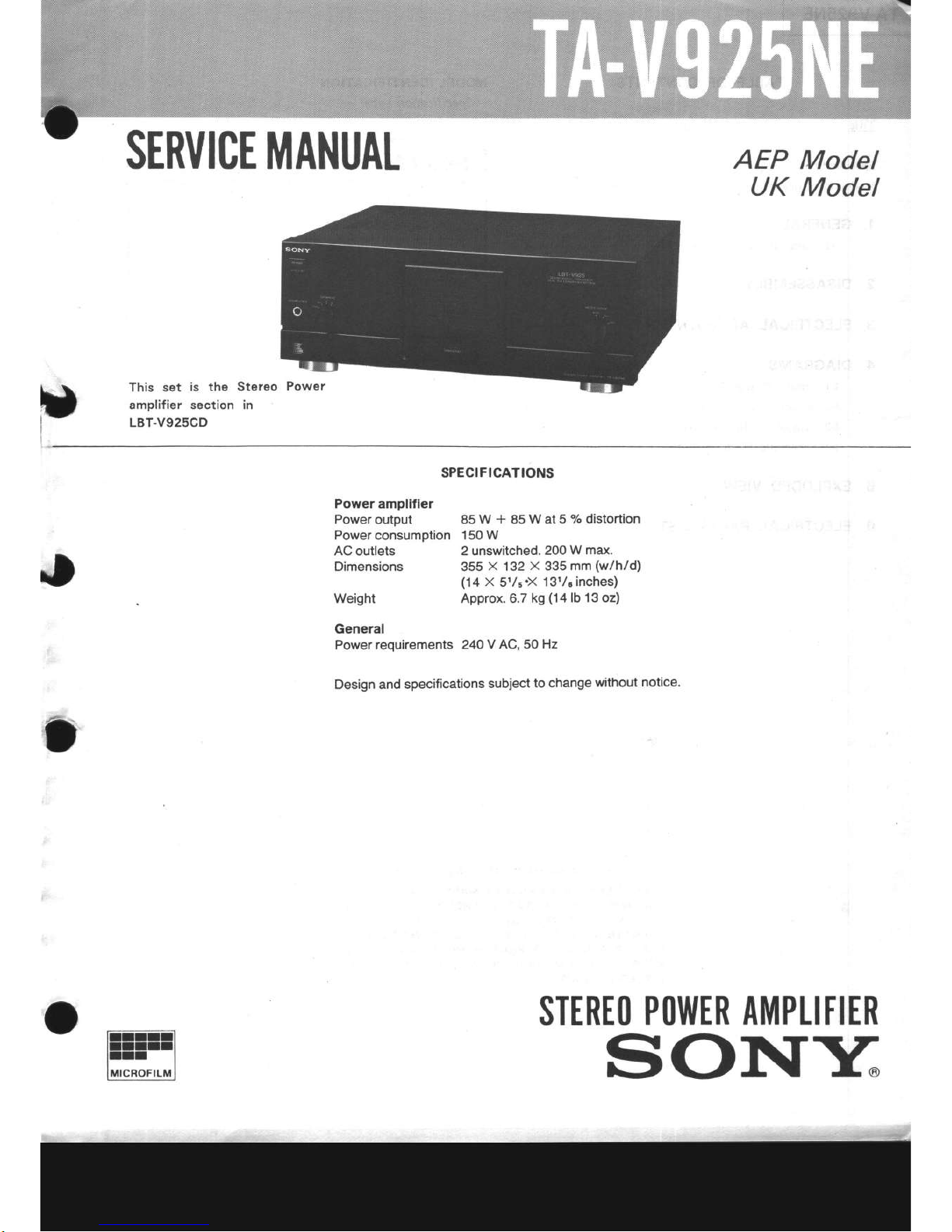
This
set
is the
Stereo
amplifier section in
LBT-V925CD
AEP
Model
UK
Model
SPECIFICATIONS
Power
amplifler
Poweroutput
85W + 85Wat5
% distortion
Power
consumption
150 W
AC
outlets
Dimensions
Weight
2 unswitched.
200
W max.
355
x
132
X
335
mm
(w/h/d)
(14
X
5rl5X
13rlcinches)
Approx. 6.7
kg
(14lb
13 oz)
General
Power
requirements 240
V AC, 50
Hz
Design and
specifications
subject
to change
without
notice.
STEREO
POtllER
AMPLITIER
SONY.
Title
Page
I.
GENERAL
1-1. Function of Controls......i.........'.......'.".."."'.."
3
4. DIAGRAMS
4-1.
Circuit
Boards Location
....".."..".5
4-2.
Semiconductors
Lead Layout...........'......'.....'..'
6
4-3. Printed
'ffiring
Boards
......'...'....'.7
44. Schematic
Diagram.......
......'.......
1l
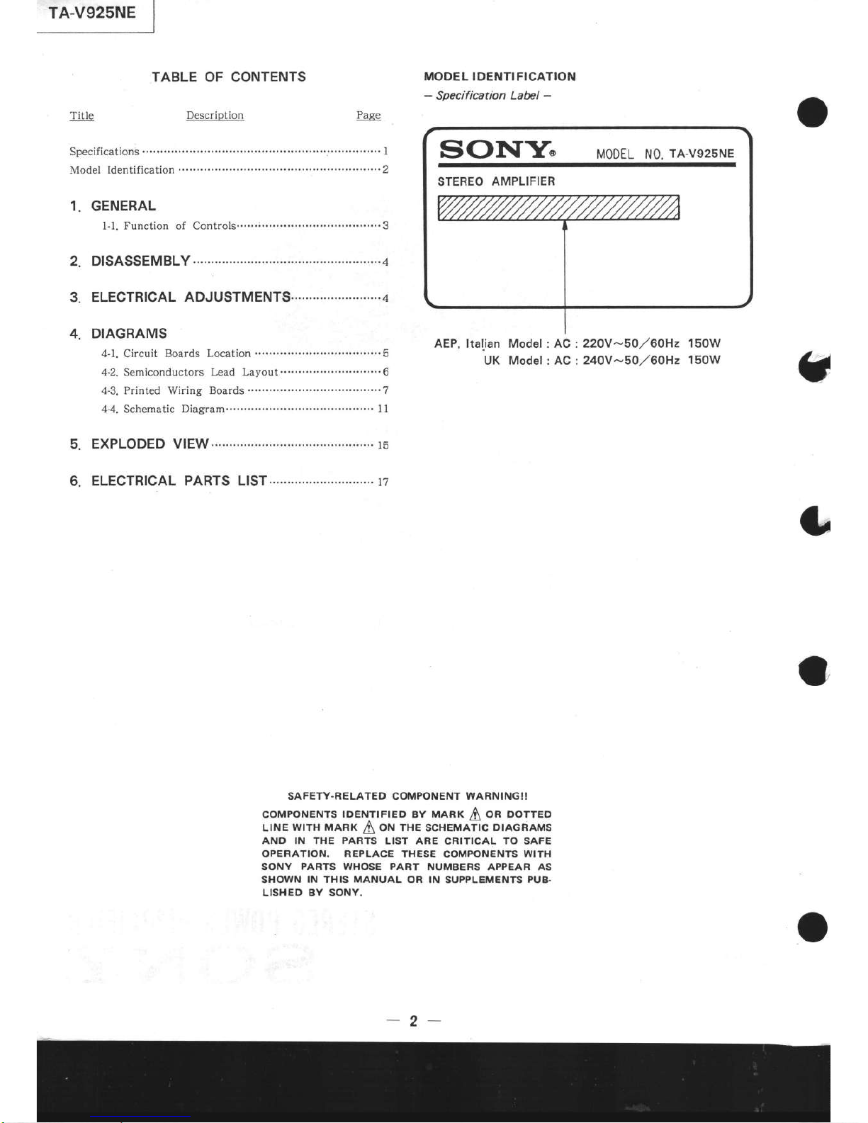
MODEL IDENTIFICATION
-
Specification
Labet
-
AEP, ltalian Model : AC:22OY-50,/60H2
150W
UK Model:
AC : 240V-50,/60H2
150W
TABLE OF CONTENTS
Description
o
M0DEL N0.
TA-V925NE
STEREO
AMPLIFIER
SAFETY.RELATED COMPONENT WARNINGI I
coMPoNENTS
|DÊNTTFTED BY MARK
2[
On OOrreO
L|NE
W|TH MARK
l\
ON THE SCHEMATTC
DTAGRAMS
AND IN THE PARTS
LIST ARE CR]TICAL TO SAFE
OPERATION. REPLACE THESE
COMPONENTS
WITH
SONY
PARTS
WHOSE PART
NUMBERS APPEAR AS
SHOWN
IN THIS MANUAL
OR IN SUPPLEMENTS
PUB.
LISHED BY SONY.
-2-
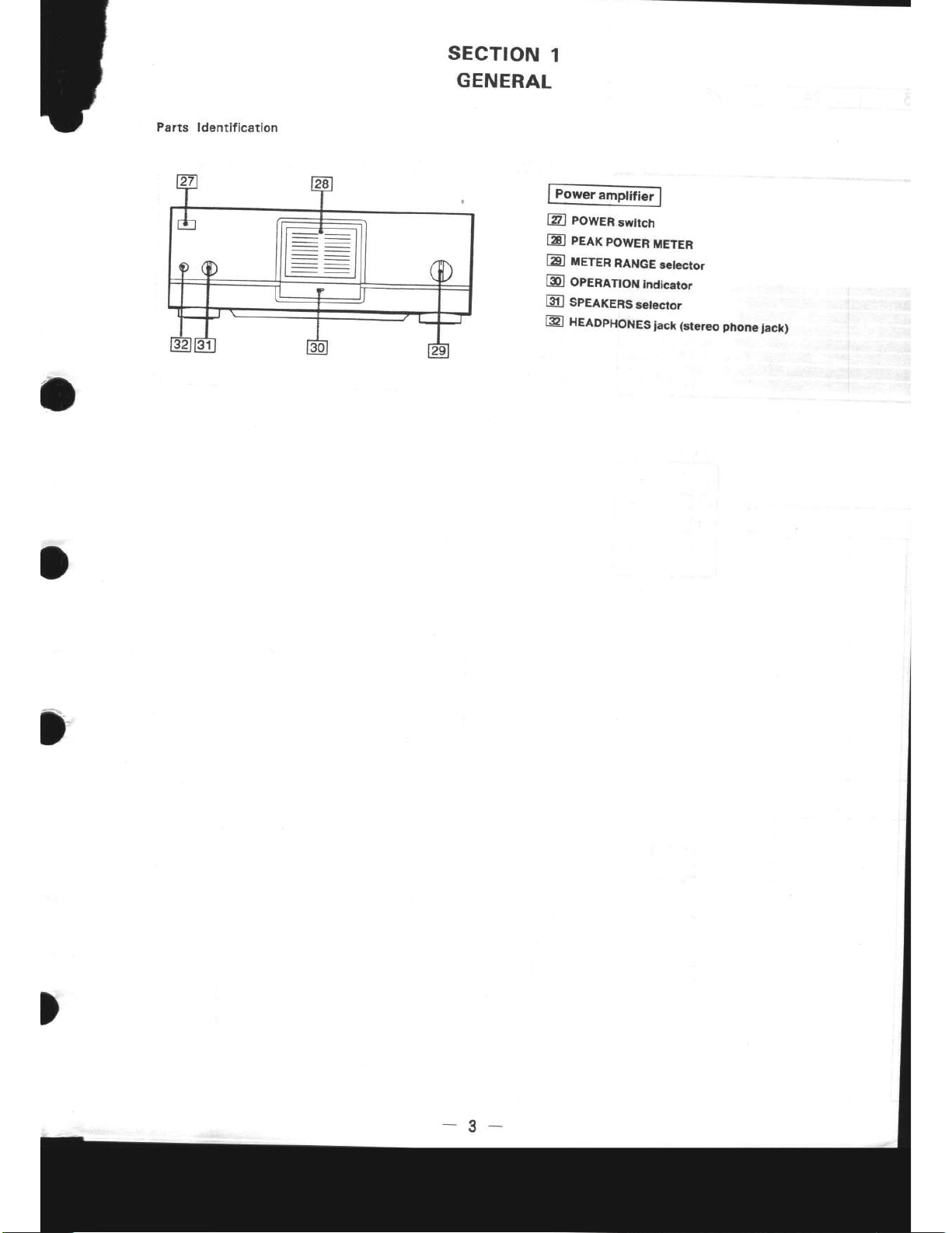
sEcTtoN
I
GENERAL
Parts
ldentification
Power
amplifier
iUl
powER
swtrch
El
peax
powEn
METER
EJ
ueren
RANGE
setecror
[S'l
openlnoN
Indtcaror
lEl
speerens
setector
lEl
XeaopXONESlack
(srereo
phone
jack)
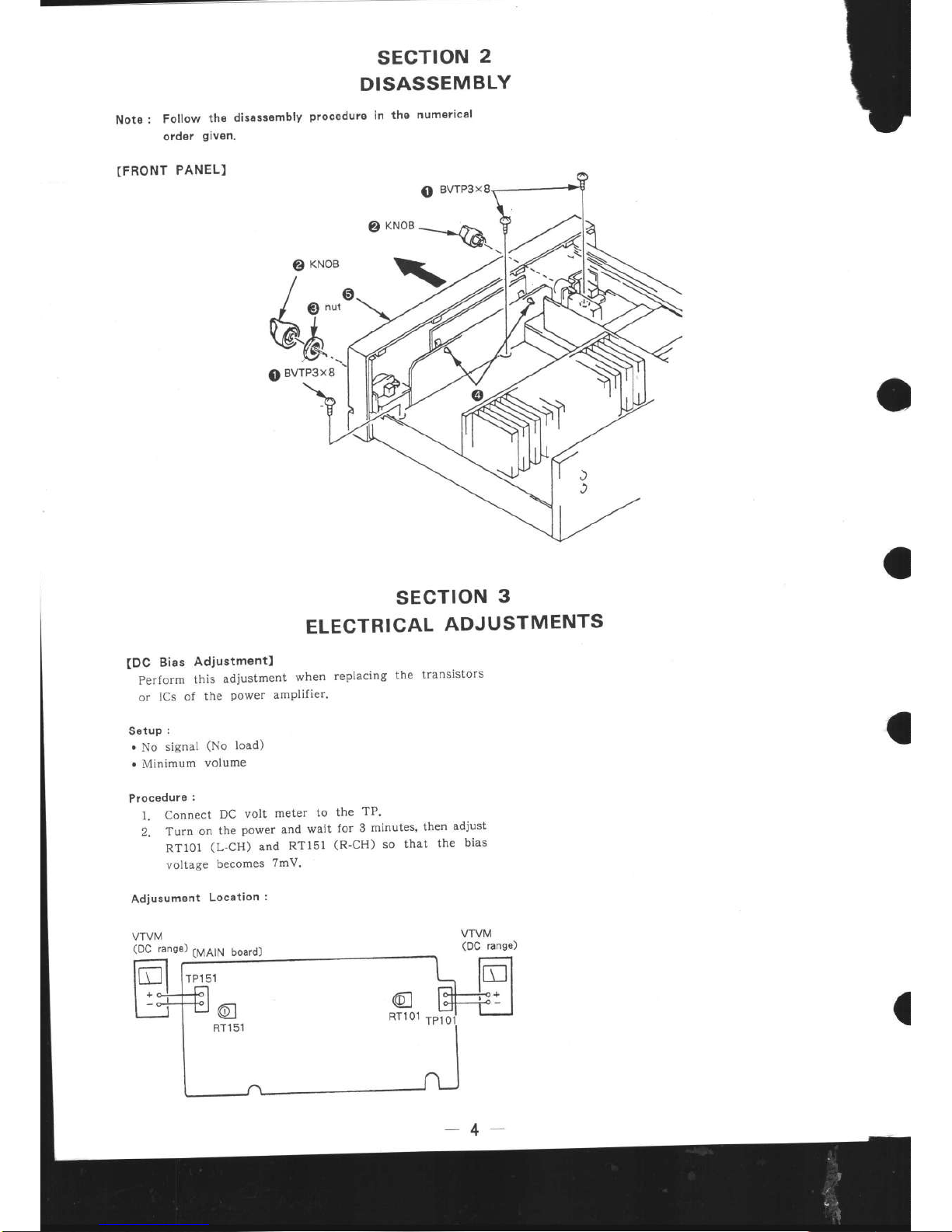
Note :
Follow
the
disassemblY
order
given.
TFRONT
PANEL]
(DC
Bias
Adjustment)
Perform
this
adjustment
when
or
ICs of
the
Power
amPlifier.
Setup
:
.
No
signal
(No
load)
.
Minimum
volume
Procedure
:
1.
Connect
DC
volt
meter
to
2.
Turn
on
the
Power
and
wait
RT101
(L-CH)
and
RTlSl
voltage
becomes
7mV.
Adjusument
Location
:
VTVM
(DC
range)
(MA1N
boardl
m
sEcTloN
2
DISASSEMBLY
proceduro
in
the
numerical
o
BVTP3XS
eKNoB--*âà
e)
KNoB
sEcrloN
3
ELECTRICAL
ADJUSTMENTS
replacing
the
transistors
the
TP.
for
3
minutes,
then
adjust
(R-CH)
so
that
the
bias
/
u*,
@À
Kt l,
F1
\ÈLJ
I
\ZJ
RT1o1
rpi
I
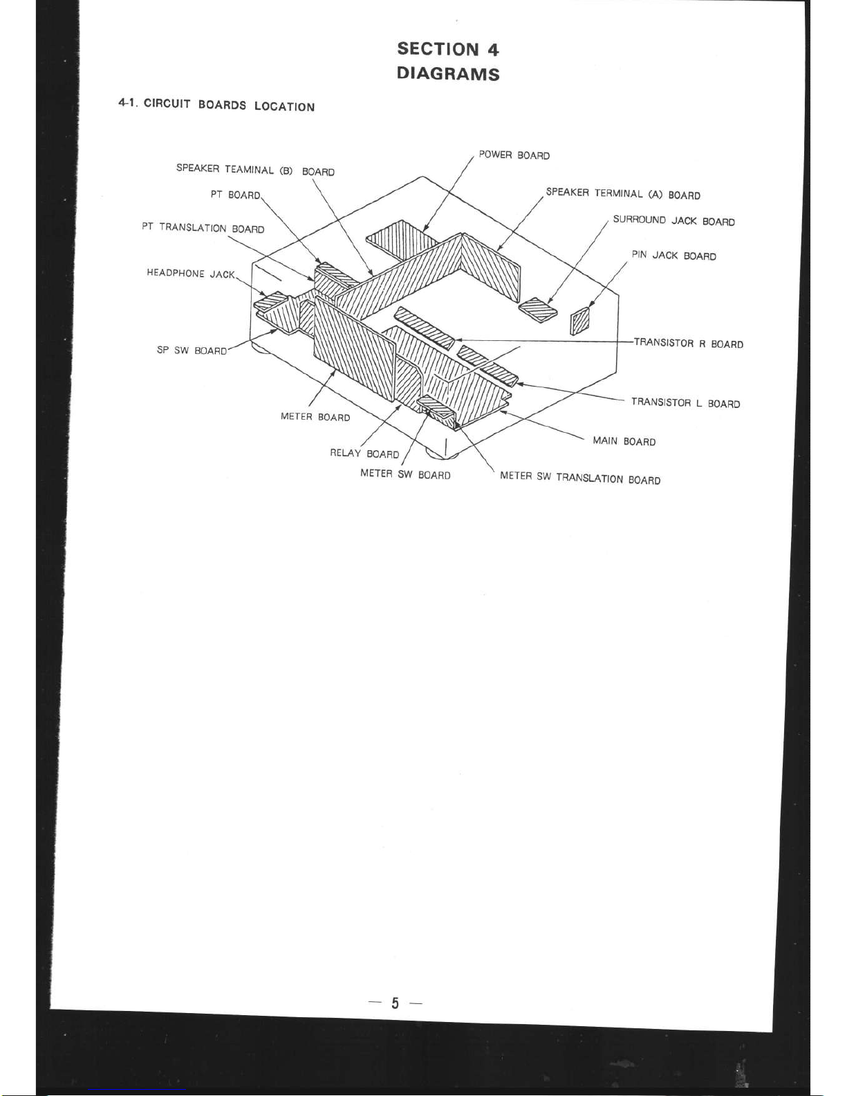
SECTION
4
DIAGRAMS
.Ll.
CIRCUIT
BOARDS
LOCATION
SPEAKER
TEAMINAL (B)
BOARD
PT
PT
TRANSLATION
BOARO
HEADPHONE
JACK
SP
SW
BOARD
METER
BOARD
POWER
BOARD
SPEAKER
TERMINAL (A)
BOARO
SURROUND
JACK
EOARO
PIN
JACK
BOARO
TRANSISTOR
R
BOARO
TRANSISTOR
L
BOARD
MAIN
BOARD
RELAY
BOARD
METER
SW
BOARD
METER
SW
TRANSLATION
BOARD
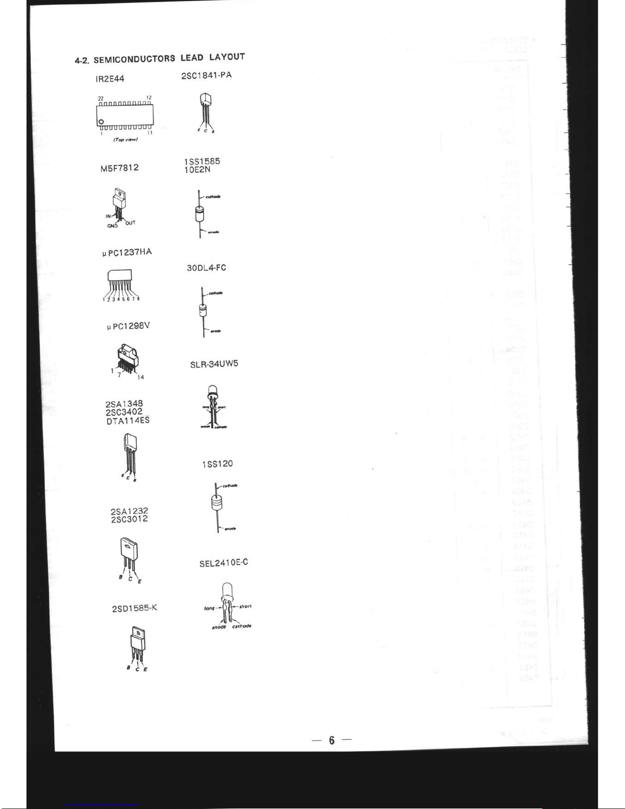
LEAD
LAYOUT
2SC1
841-PA
/h
lN
/t\
+2.
SEMICONDUCTORS
I
1
SS1
585
1 OEzN
_,::,-:"
N
':#"",
u
PC1
237H4
V*-
e
V
l-*
30DL4-FC
ï*
l-
m
u
PC1
298V
,'m,a
2SA1
348
25C3402
DTAl
14ES
n:r
ffi[
altl
SLR-34UW5
fr
1 SS1
20
lz-ta
g
I
I
F--
SEL241OE-C
n
'""''ft'"^
a6&
cthode
25A1232
2SC301
2
t\
,'ry'.
2S01585-K
N
,[{.
 Loading...