Sony TAN-9000-ES Service manual
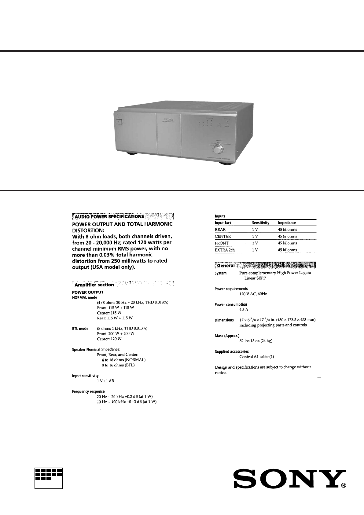
TA-N9000ES
SERVICE MANUAL
Photo: GOLD model
SPECIFICATIONS
US Model
Canadian Model
AEP Model
UK Model
E Model
Australian Model
Chinese Model
MICROFILM
5 CHANNEL POWER AMPLIFIER

T ABLE OF CONTENTS
1. SERVICING NOTES ............................................... 3
2. GENERAL ................................................................... 4
3. DISASSEMBLY ......................................................... 5
4. ELECTRICAL ADJUSTMENTS......................... 7
5. DIAGRAMS................................................................. 8
5-1. Note for Printed Wiring Boards and
Schematic Diagrams ....................................................... 9
5-2. Printed Wiring Boards – MAIN Section – .................... 11
5-3. Schematic Diagram – MAIN Section (1/3) –................ 13
5-4. Schematic Diagram – MAIN Section (2/3) –................ 15
5-5. Schematic Diagram – MAIN Section (3/3) –................ 17
5-6. Printed Wiring Boards – CONTROL Section – ............ 19
5-7. Schematic Diagram – CONTROL Section –................. 21
5-8. Printed Wiring Boards – POWER Section – ................. 23
5-9. Schematic Diagram – POWER Section – ..................... 25
5-10. IC Pin Function Description ........................................... 27
6. EXPLODED VIEWS ................................................ 28
7. ELECTRICAL PARTS LIST ............................... 30
SAFETY-RELA TED COMPONENT W ARNING!!
COMPONENTS IDENTIFIED BY MARK ! OR DOTTED
LINE WITH MARK ! ON THE SCHEMATIC DIAGRAMS
AND IN THE PARTS LIST ARE CRITICAL TO SAFE
OPERATION. REPLACE THESE COMPONENTS WITH
SONY PARTS WHOSE PART NUMBERS APPEAR AS
SHOWN IN THIS MANUAL OR IN SUPPLEMENTS PUBLISHED BY SONY .
A TTENTION A U COMPOSANT AYANT RAPPORT
À LA SÉCURITÉ!
LES COMPOSANTS IDENTIFIÉS P AR UNE MARQUE !
SUR LES DIAGRAMMES SCHÉMATIQUES ET LA LISTE
DES PIÈCES SONT CRITIQUES POUR LA SÉCURITÉ
DE FONCTIONNEMENT. NE REMPLACER CES COMPOSANTS QUE PAR DES PIÈCES SONY DONT LES
NUMÉROS SONT DONNÉS DANS CE MANUEL OU
DANS LES SUPPLÉMENTS PUBLIÉS PAR SONY.
– 2 –
SECTION 1
8
SERVICING NOTES
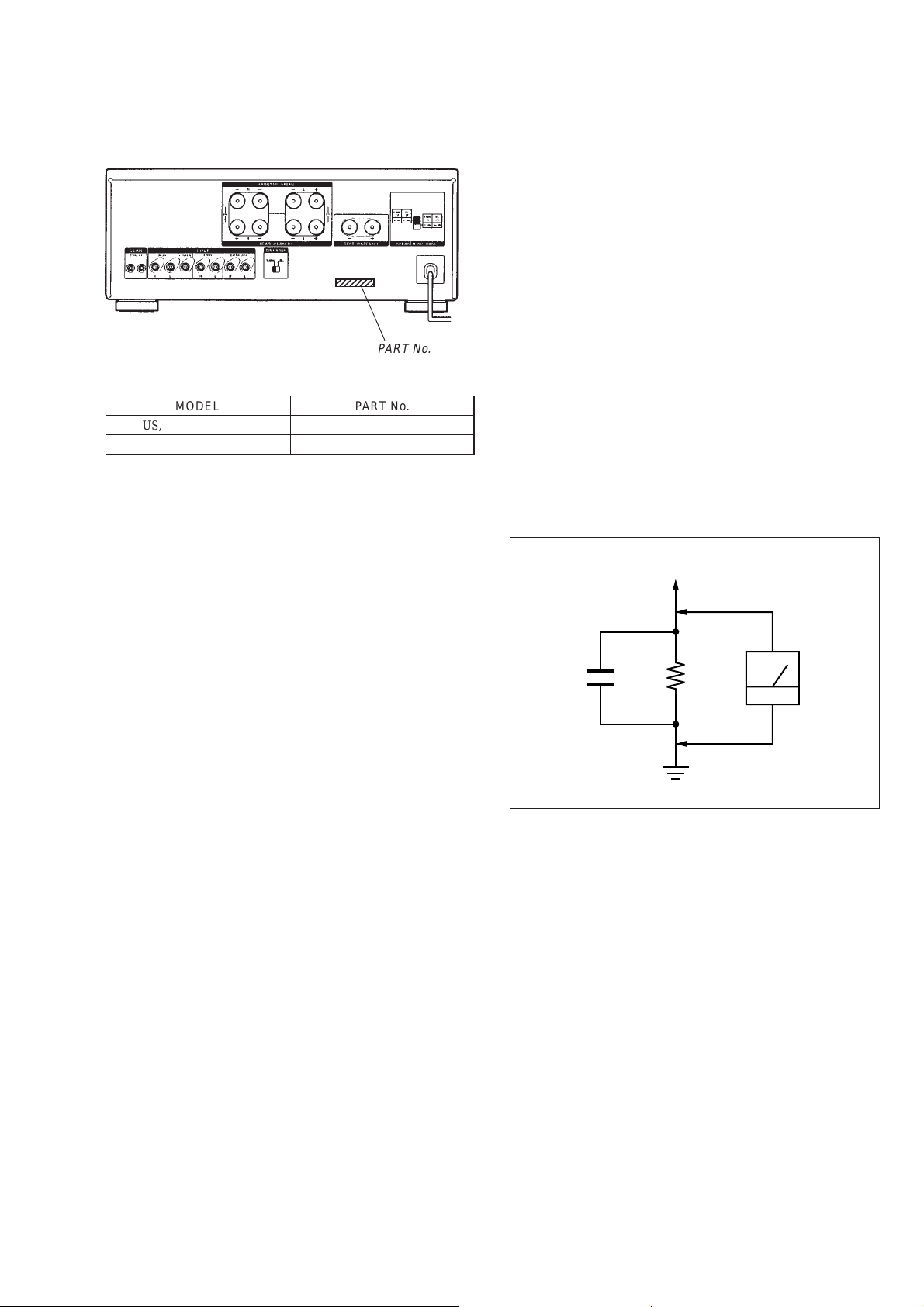
MODEL IDENTIFICATION
– Rear view –
234567
PART No.
MODEL PART No.
US, Canadian models 4-211-114-1π
Except US, Canadian models 4-211-114-2π
Notes on chip component replacement
• Never reuse a disconnected chip component.
• Notice that the minus side of a tantalum capacitor may be damaged by heat.
SAFETY CHECK-OUT
After correcting the original service problem, perform the following safety check before releasing the set to the customer:
Check the antenna terminals, metal trim, “metallized” knobs,
screws, and all other exposed metal parts for AC leakage.
Check leakage as described below.
LEAKAGE TEST
The AC leakage from any exposed metal part to earth ground and
from all exposed metal parts to any exposed metal part having a
return to chassis, must not exceed 0.5 mA (500 microampers.).
Leakage current can be measured by any one of three methods.
1. A commercial leakage tester , such as the Simpson 229 or RCA
WT -540A. Follo w the manufacturers’ instructions to use these
instruments.
2. A battery-operated AC milliammeter. The Data Precision 245
digital multimeter is suitable for this job.
3. Measuring the voltage drop across a resistor by means of a
VOM or battery-operated AC voltmeter. The “limit” indication is 0.75 V, so analog meters must have an accurate lowvoltage scale. The Simpson 250 and Sanwa SH-63Trd are examples of a passive VOM that is suitable. Nearly all battery
operated digital multimeters that have a 2 V A C range are suitable. (See Fig. A)
To Exposed Metal
Parts on Set
1.5 k
0.15 µF
Fig. A. Using an AC voltmeter to check AC leakage.
Ω
Earth Ground
AC
voltmeter
(0.75 V)
– 3 –
SECTION 2
GENERAL
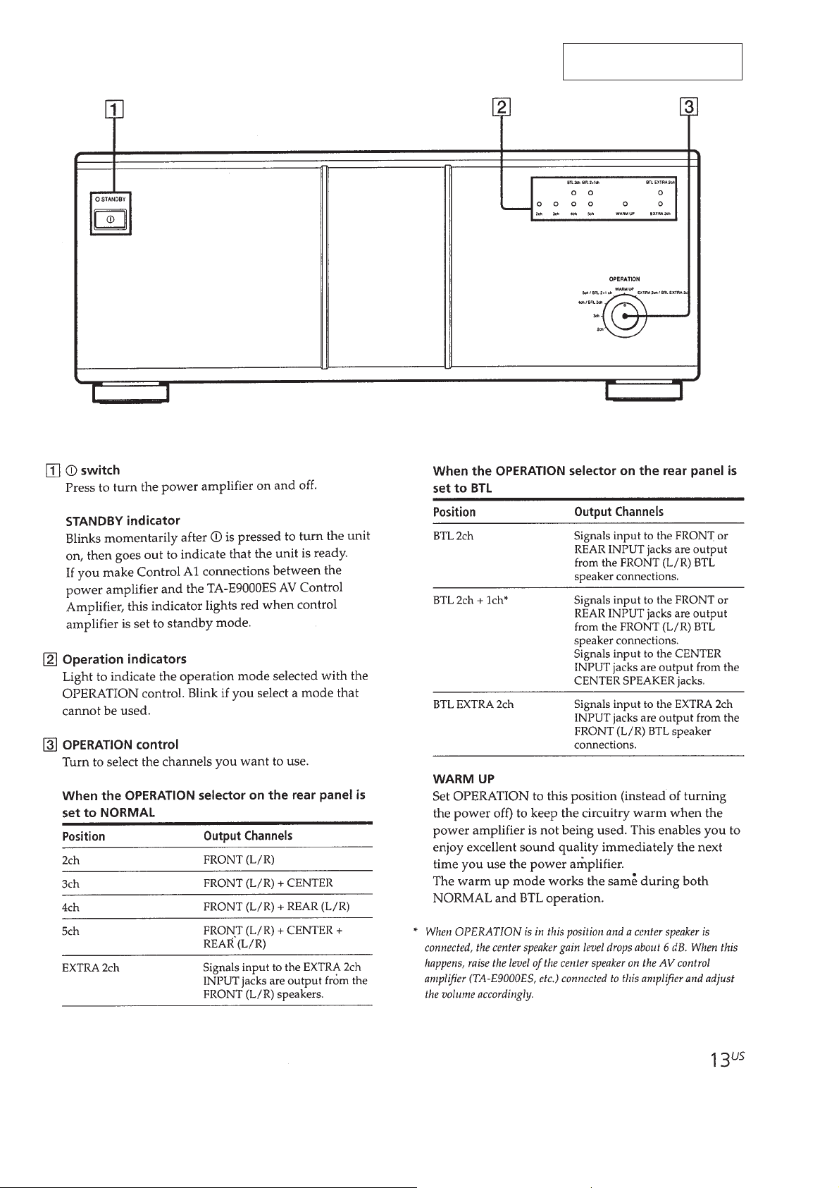
This section is extracted from
instruction manual.
– 4 –
SECTION 3
s
DISASSEMBLY
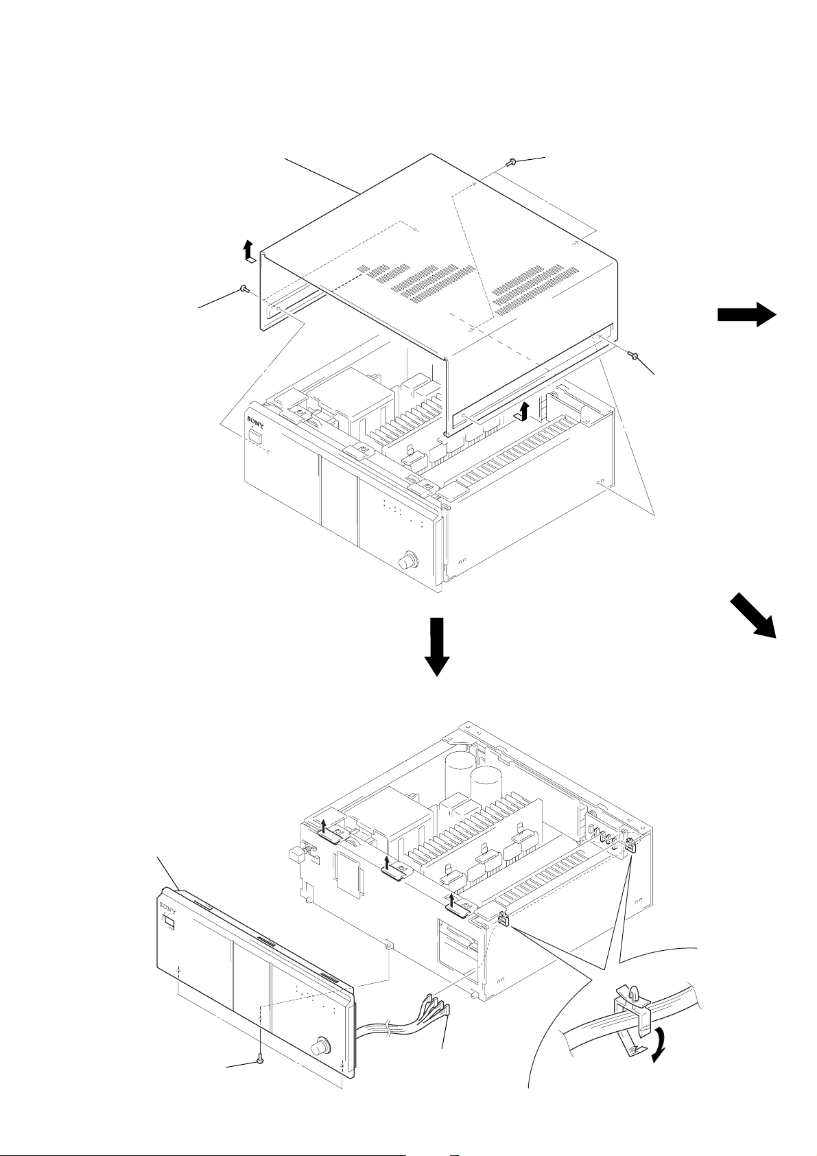
Note: Follow the disassembly procedure in the numerical order given.
CASE
3
case
2
two flat head screws
1
two screws
(BV3 x 8B)
2
two flat head screw
FRONT PANEL SECTION
front panel section
5
3
three screws
(BV3
×
8B)
4
4
4
2
four connectors
(CN152, 153, 154, 155)
1
Unlock each claw of the saddle wire.
– 5 –
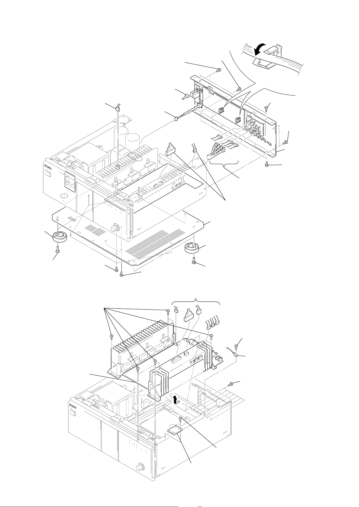
BOTTOM PLATE, BACK PANEL SECTION
6
connector
(CN808)
6
connector
(CN812)
8
6
connector
(CN809)
two screws
(BV3
×
8B)
9
two screws
(P4
×
8)
6
two connectors
(CN201, 205)
5
Unlock each claw of
the saddle wire.
7
6
seven connectors
(CN152, 153, 154,
155, 156, 157, 158)
two screws
(K3
×
8)
8
two screws
(BV3
0
back panel
section
8
two screws
(BV3
×
×
8B)
8B)
2
two foot assy’s
1
two screws
(B4
MAIN BOARD
×
16)
7
3
six screws
(BV3
6
ten screws
(BV3
MAIN board
×
×
8B)
8B)
3
two screws
(BV3
4
bottom plate
2
two foot assy’s
1
two screws
×
8B)
1
six connectors
(CN101, 201, 202, 203, 204, 205)
(B4
×
16)
4
screw
(BV3
5
lug
6
seven screws
(BV3
×
×
8B)
8B)
– 6 –
3
bracket
2
two screws
(BV3
×
8B)
SECTION 4
ELECTRICAL ADJUSTMENTS
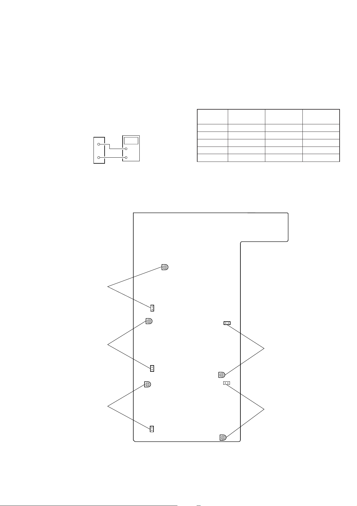
DC BIAS CURRENT Adjustment
(with no signal input)
After replacing the power transistors, DC BIAS CURRENT adjustments should be perfomed.
Setting:
SPEAKER IMPEDANCE switch (S801): 8 Ω MIN (NORMAL
USE)
Procedure:
MAIN BOARD
(CN301, 401, 501,
601, 701)
2
1
Note: After adjustment, check five connecting points.
Tester
+
–
Adjustment Location:
[MAIN Board]
(Component Side)
Connecting Adjustment Reading on
point part the tester
FRONT Lch CN601 RV601 11 ±1 mA
FRONT Rch CN701 RV701 11 ±1 mA
CENTER CN501 RV501 11 ±1 mA
REAR Lch CN301 RV301 11 ±1 mA
REAR Rch CN401 RV401 11 ±1 mA
RV601
FRONT Lch
CENTER
FRONT Rch
RV501
RV701
1
CN601
2
1
CN501
2
1
CN701
2
CN401
1
RV401
1
CN301
RV301
2
REAR Rch
2
REAR Lch
– 7 –

• Circuit Boards Location
d
SECTION 5
DIAGRAMS
RY board
SW board
PS board
SP board
LED board
AC-SW board
AC board
BIAS-FL board
CONTROL board
JOINT board
BIAS-FR boar
BIAS-RR board
MAIN board
BIAS-C board
BIAS-RL board
– 8 –
TA-N9000ES
3.8 Vp-p
8 MHz
5-1. NOTE FOR PRINTED WIRING BOARDS AND SCHEMA TIC DIAGRAMS
Note on Printed Wiring Board:
• X : parts extracted from the component side.
• b : Pattern from the side which enables seeing.
• Indication of transistor.
C
Q
B
E
These are omitted.
Q
B
CE
These are omitted.
Note on Schematic Diagram:
• All capacitors are in µF unless otherwise noted. pF: µµF
50 WV or less are not indicated except for electrolytics
and tantalums.
• All resistors are in Ω and 1/
specified.
¢
•
: internal component.
4
W or less unless otherwise
• 5 : fusible resistor.
• C : panel designation.
Note:
The components identified by mark ! or dotted
line with mark ! are critical for safety.
Replace only with part
number specified.
Note:
Les composants identifiés par
une marque ! sont critiques
pour la sécurité.
Ne les remplacer que par une
piéce portant le numéro
spécifié.
• U : B+ Line.
• V : B– Line.
• H : adjustment for repair.
• Voltages and waveform are dc with respect to ground
under no-signal conditions.
• Voltages and waveforms are taken with a VOM (Input
impedance 10 MΩ).
Voltage variations may be noted due to normal production tolerances.
• Waveforms are taken with a oscilloscope.
Voltage variations may be noted due to normal production tolerances.
• Circled numbers refer to waveforms.
• Signal path.
F : AUDIO
• Abbreviation
CND : Canadian model.
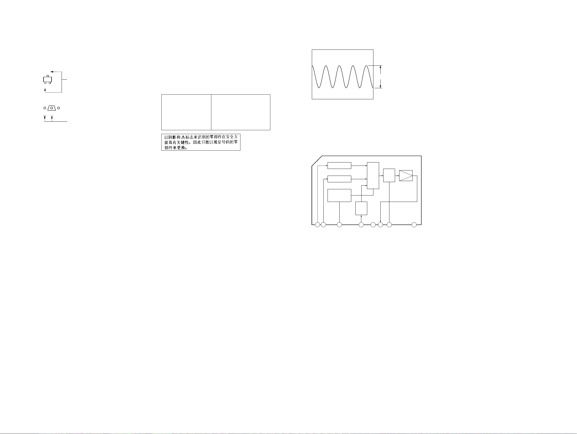
• Waveform
1 IC901 @º (X-OUT)
• IC Block Diagram
– MAIN BOARD –
IC201 µPC1237HA
OVER LOAD DET
OFFSET DET
LATCH/
AUTORESET
1 2 3
V
CC
MUTE
ON
F/F
AC OFF
DET
4 5 6 7 8
V
CC
– 9 – – 10 –
 Loading...