Sony TA FE370, TA FE570 Service Manual
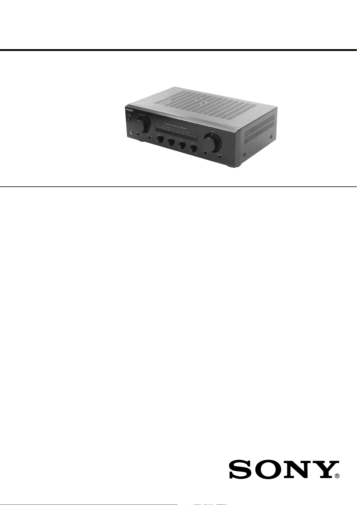
TA-FE370/FE570
SERVICE MANUAL
Ver 1.0 2001.04
Photo: TA-FE570 (BLACK)
SPECIFICATIONS
Amplifier section
DIN power output
TA-FE570: 110 W + 110 W
TA-FE370: 70 W + 70 W
Frequency response
PHONO (20 Hz - 20 kHz): RIAA equalization curve
TUNER, CD, AUX, TAPE1/DAT, TAPE2/MD:
S/N (network A)
PHONO: 80 dB
TUNER, CD, AUX, TAPE1/DAT, TAPE2/MD:
Output voltage/impedance
RECOUT: 200 mV, 1 kilohm
PHONES: 5 mW (at 8 ohms)
Speakers impedance 4 - 16 ohms
Damping factor 80 (8 ohms, 1 kHz)
(4 ohms at 1 kHz)
(4 ohms at 1 kHz)
±1.0 dB
7 Hz - 70 kHz
105 dB
+–03
dB
General
System
Power amplifier with all stages directly coupled
Preamplifier: Low-noise, equalizer
Power requirements 230 V AC, 50/60 Hz
Power consumption
TA-FE570: 190 W
TA-FE370: 160 W
Dimensions (approx.) (w/h/d)
Mass (approx.)
TA-FE570: 6.5 kg
TA-FE370: 5.5 kg
Supplied accessories
Remote commander (remote) RM-S325 (1)
Sony batteries R6 (size-AA) (2)
Design and specifications are subject to change
without notice.
amplifier
0.6 W
(In standby mode)
430 x 135 x 310 mm
incl. projecting parts and
controls
AEP Model
UK Model
9-873-838-11 Sony Corporation
2001D0500-1 Home Audio Company
C 2001.4 Shinagawa Tec Service Manual Production Group
INTEGRATED STEREO AMPLIFIER
TA-FE370/FE570
SECTION 1
SERVICING NOTES
TABLE OF CONTENTS
1. SERVICING NOTES ............................................... 2
2. GENERAL
Location of Controls ....................................................... 3
3. DISASSEMBLY
3-1. Disassembly Flow ........................................................... 4
3-2. Case ................................................................................. 4
3-3. Front Panel Assy ............................................................. 5
3-4. MAIN Board ................................................................... 5
4. DIAGRAMS
4-1. Note for Printed Wiring Boards
and Schematic Diagrams ................................................ 7
4-2. Printed Wiring Board – MAIN Board – ........................ 8
4-3. Schematic Diagram – MAIN Board – ............................ 9
4-4. Printed Wiring Boards – CONTROL/SPEAKER SW/
VOLUME/Boards – ........................................................ 10
4-5. Schematic Diagram – CONTROL/SPEAKER SW/
VOLUME Boards – ........................................................ 11
4-6. Printed Wiring Boards
– AC OUTLET/HEADPHONE/LOUDNESS/
POWER SW/STANDBY Boards –................................. 12
4-7. Schematic Diagram
– AC OUTLET/HEADPHONE/LOUDNESS/
POWER SW/STANDBY Boards –................................. 13
4-8. IC Pin Function Description ........................................... 14
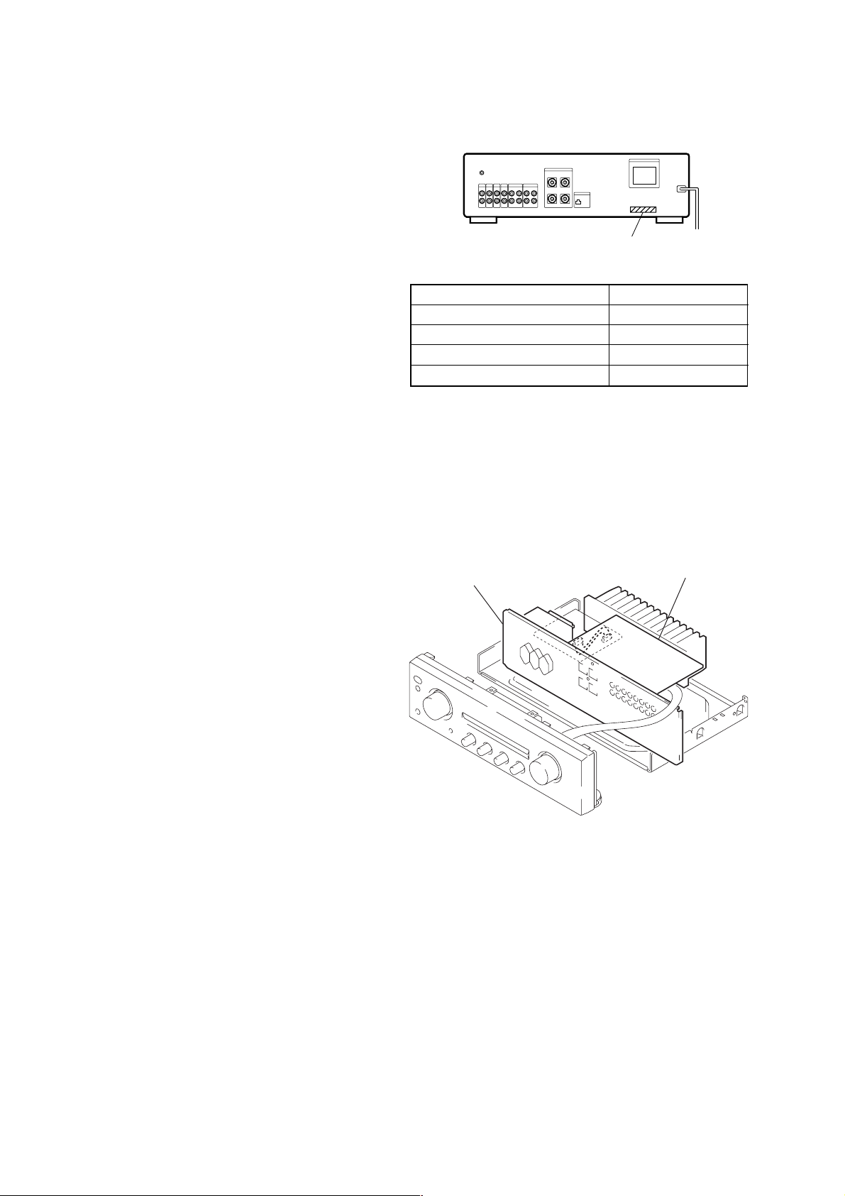
MODEL IDENTIFICATION
– Back Panel –
AC OUTLET
A
N
G
I
S
D
N
G
L
U
PHONOINTUNER
IN
L
R
CD AUX TAPE2/MD TAPE1/DAT
RECOUT
IN
IN IN
RECOUT
IN
SPEAKERS
IMPEDANCE USE 4 - 16 Ω
RL
+–+
EON CONTROL
IN
–
SWITCHED 100W MAX
PART No.
Model PART No.
T A-FE570: AEP model 4-233-359-0
TA-FE570: UK model 4-233-359-1
T A-FE370: AEP model 4-233-359-2
TA-FE370: UK model 4-233-359-3
[]
[]
[]
[]
MAIN BOARD SETTING
On AEP model of this set, A C outlet is mounted onto the A C OUT LET board holding the back panel between. Since removing the
MAIN board alone is difficult, in repairing the MAIN board, handle
the MAIN board with the back panel connected as shown in the
figure below.
5. EXPLODED VIEWS
5-1. Case Section .................................................................... 15
5-2. Front Panel Section ......................................................... 16
5-3. Chassis Section ............................................................... 17
6. ELECTRICAL PARTS LIST ............................... 18
back panel
MAIN board
SAFETY-RELATED COMPONENT WARNING!!
COMPONENTS IDENTIFIED BY MARK 0 OR DOTTED
LINE WITH MARK 0 ON THE SCHEMATIC DIAGRAMS
AND IN THE PARTS LIST ARE CRITICAL TO SAFE
OPERATION. REPLACE THESE COMPONENTS WITH
SONY PARTS WHOSE PART NUMBERS APPEAR AS
SHOWN IN THIS MANUAL OR IN SUPPLEMENTS PUBLISHED BY SONY.
2
TA-FE370/FE570
)
• This set can be disassembled in the order shown below.
3-1. DISASSEMBLY FLOW
SET
3-2. CASE
(Page 4)
3-3. FRONT PANEL ASSY
(Page 5)
3-4. MAIN BOARD
(Page 5)
SECTION 3
DISASSEMBLY
Note: Follow the disassembly procedure in the numerical order given.
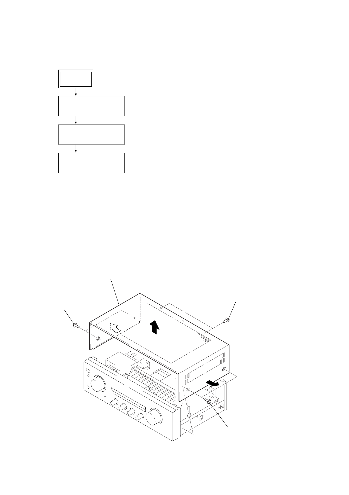
3-2. CASE
3
case
1
two screws
(case 3 TP2)
2
2
1
two screws
(case 3 TP2
1
two screws
(case 3 TP2)
4
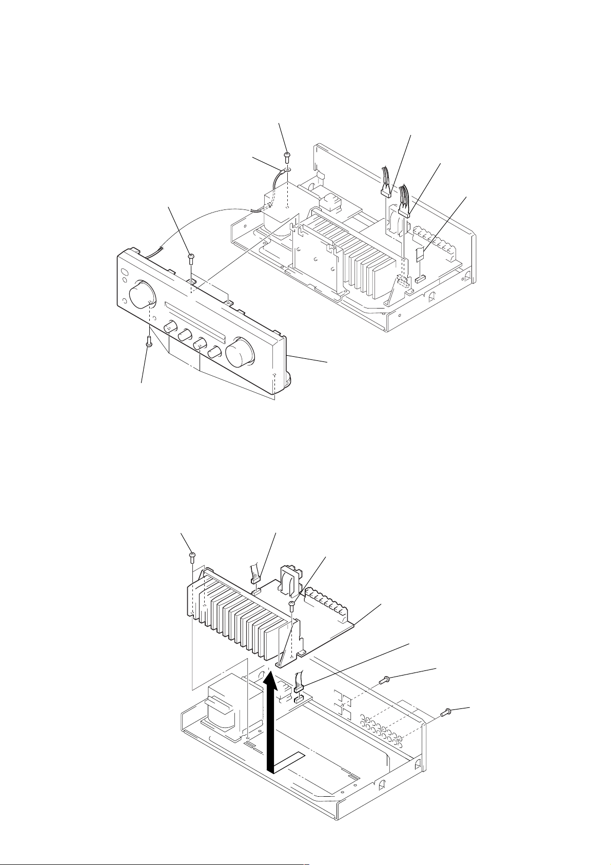
3-3. FRONT PANEL ASSY
5
two screws
(BVTP3
×
8)
6
four screws
(BVTP3 × 8)
3
screw
(BVTP3
×
8)
1
connector (CN811)
4
harness
1
connector (CN812)
2
wire (flat type) (15 core)
(CN815)
7
front panel assy
TA-FE370/FE570
3-4. MAIN BOARD
3
two screws
(BVTP3
2
×
8)
connector (CN901)
4
two screws
(BVTP3
×
8)
5
MAIN board
1
connector (CN902)
3
screw
(BVTP3
×
8)
3
three screws
(BVTP3
×
8)
5
SECTION 4
DIAGRAMS
TA-FE370/FE570
4-1. NOTE FOR PRINTED WIRING BOARDS AND SCHEMATIC DIAGRAMS
Note on Printed Wiring Board:
• X : parts extracted from the component side.
• : Pattern from the side which enables seeing.
(The other layers' patterns are not indicated.)
• Indication of transistor
Q
B
CE
These are omitted.
Q
B
CE
These are omitted.
Note on Schematic Diagram:
• All capacitors are in µF unless otherwise noted. pF: µµF
50 WV or less are not indicated except for electrolytics
and tantalums.
• All resistors are in Ω and 1/
specified.
f
•
• 2 : nonflammable resistor.
• C : panel designation.
Note: The components identified by mark 0 or dotted line
• A : B+ Line.
• B : B – Line.
• Voltages and waveforms are dc with respect to ground
• Voltages are taken with a VOM (Input impedance 10 MΩ).
• Waveforms are taken with a oscilloscope.
• Circled numbers refer to waveforms.
• Signal path.
: internal component.
with mark 0 are critical for safety.
Replace only with part number specified.
under no-signal conditions.
no mark : TUNER
Voltage variations may be noted due to normal production tolerances.
Voltage variations may be noted due to normal production tolerances.
F : TUNER
E : TAPE1/DAT IN
a : RECOUT
d : TAPE2/MD IN
J : CD
I : PHONO
4
W or less unless otherwise
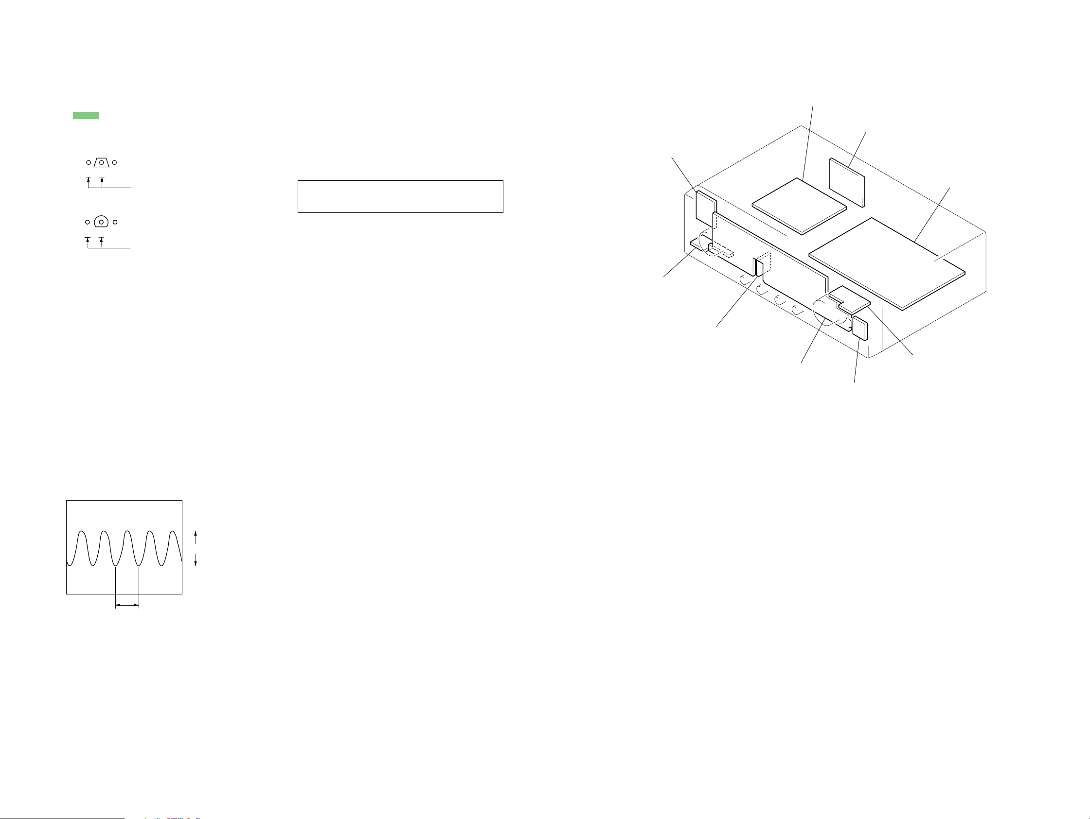
• Circuit Boards Location
STANDBY board
AC OUTLET board
POWER SW board
MAIN board
HEADPHONE board
SPEAKER SW board
VOLUME board
CONTROL board
LOUDNESS board
• Waveform
– CONTROL Board –
1 IC801 1 (XOUT)
250 ns
3 Vp-p
77
 Loading...