

TA-FE320R/FE520R
SERVICE MANUAL
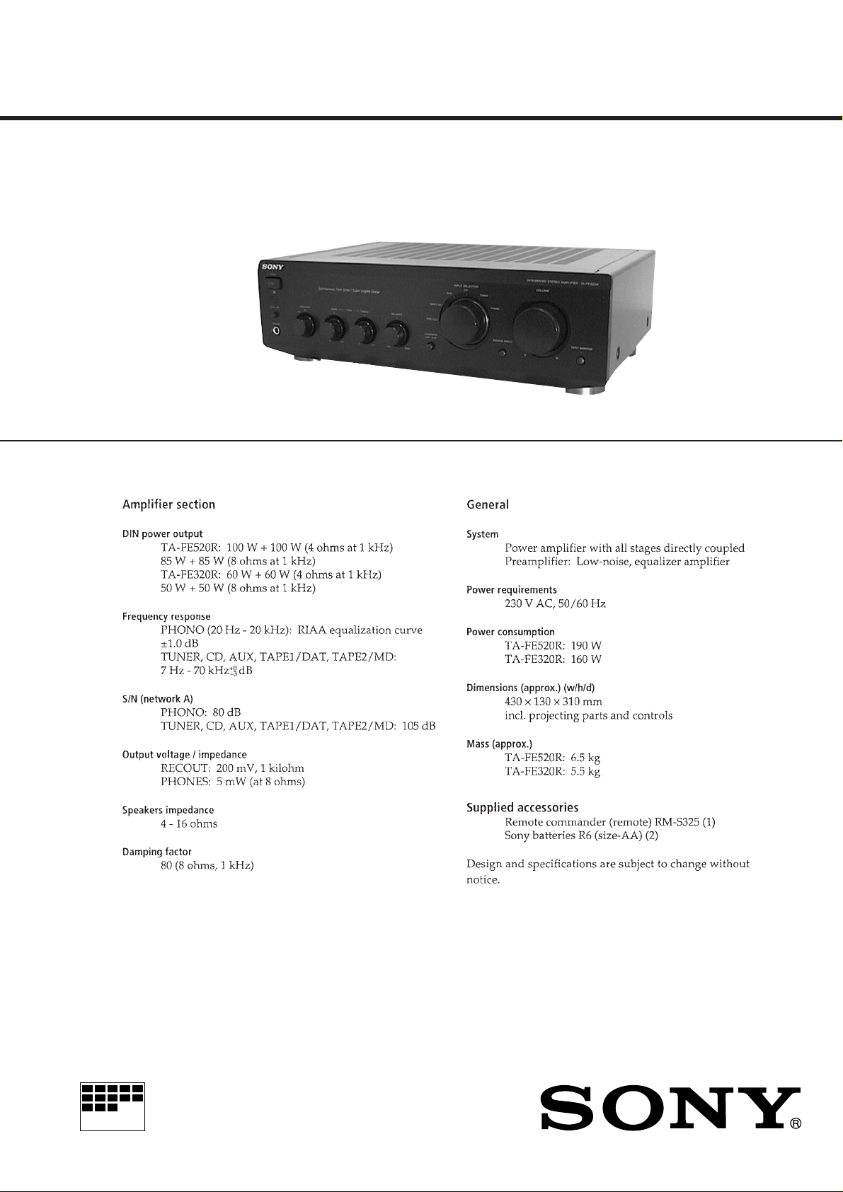
Photo: TA-FE520R
SPECIFICATIONS
AEP Model
TA-FE320R/FE520R
UK Model
TA-FE320R
MICROFILM
INTEGRATED STEREO AMPLIFIER

TABLE OF CONTENTS
1. GENERAL
Location of Controls ....................................................... 3
2. DISASSEMBLY ......................................................... 4
3. DIAGRAMS
3-1. Notes for Printed Wiring Boards
and Schematic Diagrams ................................................ 6
3-2. Printed Wiring Board – MAIN Section –...................... 7
3-3. Schematic Diagram – MAIN Section –.......................... 9
3-4. Printed Wiring Boards – PANEL Section – .................. 11
3-5. Schematic Diagram – PANEL Section –....................... 13
3-6. Printed Wiring Boards – POWER Section – ................. 15
3-7. Schematic Diagram – POWER Section – ..................... 16
3-8. IC Pin Function Description ........................................... 18
4. EXPLODED VIEWS ................................................ 19
5. ELECTRICAL PARTS LIST ............................... 21
– 2 –
SAFETY-RELATED COMPONENT WARNING!!
COMPONENTS IDENTIFIED BY MARK ! OR DOTTED
LINE WITH MARK ! ON THE SCHEMATIC DIAGRAMS
AND IN THE PARTS LIST ARE CRITICAL TO SAFE
OPERATION. REPLACE THESE COMPONENTS WITH
SONY PARTS WHOSE PART NUMBERS APPEAR AS
SHOWN IN THIS MANUAL OR IN SUPPLEMENTS PUBLISHED BY SONY.
SECTION 1
GENERAL
LOCATION OF CONTROLS
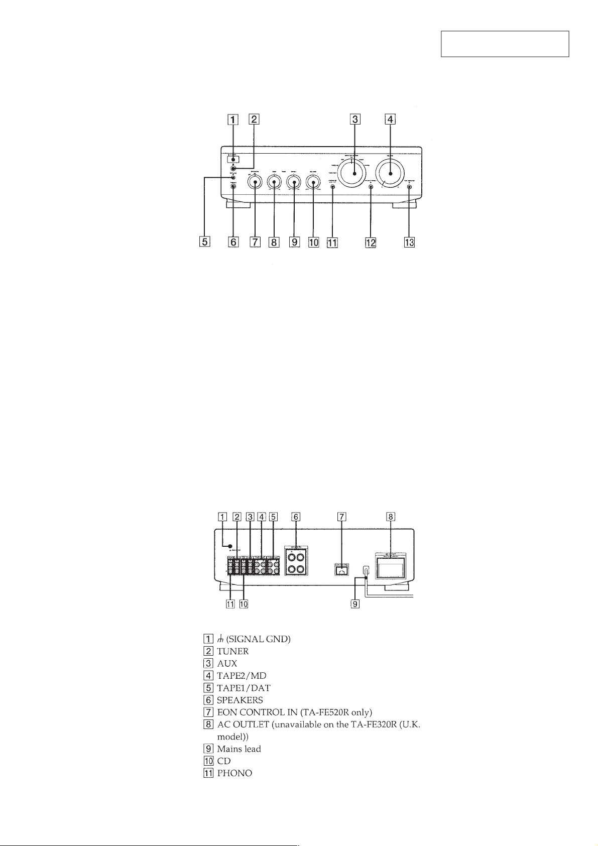
Front Panel
1 I/u (POWER) button
2 Remote control sensor
3 INPUT SELECTOR switch
4 VOLUME control
5 EON LINK button (TA-FE520R only)
6 PHONES jack
7 SPEAKERS switch
8 BASS control
9 TREBLE control
0 BALANCE control
!¡ LOUDNESS button
!™ SOURCE DIRECT button
!£ TAPE MONITOR button (TA-FE520R only)
This section is extracted from
instruction manual.
Rear Panel
– 3 –
SECTION 2
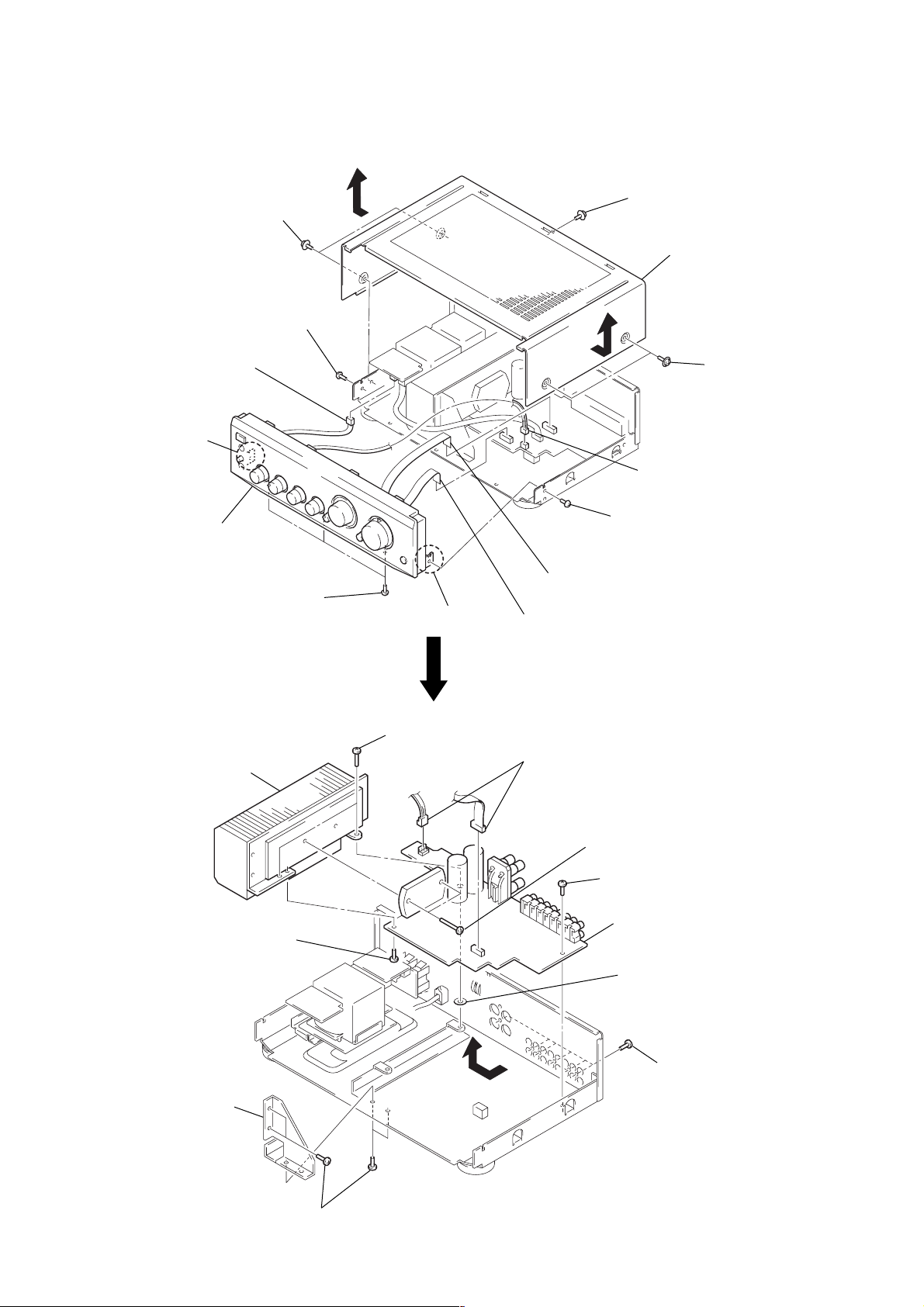
DISASSEMBLY
Note: Follow the disassembly procedure in the numerical order given.
FRONT PANEL SECTION
1
two screws
(CASE)
5
6
4
claw
screw
(BVTP3
connector
(CN902)
×
8)
1
screw
(CASE)
2
case
4
connector
(CN812) (FE520R)
1
two screws
(CASE)
MAIN BOARD
7
front panel section
0
heat sink
9
screw
(BVTP3
5
three screws
(BVTP3
×
10)
5
screw
(BVTP3
3
wire (flat type) (13 core)
×
8)
5
6
two screws
(BVTP3
×
claw
10)
(CN815)
3
wire (flat type) (13 core)
(CN811)
1
two connectors
(CN951, 952)
8
two screws
(BVTP3
4
screw
(BVTP3
!¡
×
8)
×
16)
×
8)
MAIN board
3
bracket
(HEAT SINK)
2
four screws
(BVTP3
7
washer
(FIBER DIA.10)
6
×
8)
4
six screws
(BVTP3
×
8)
– 4 –
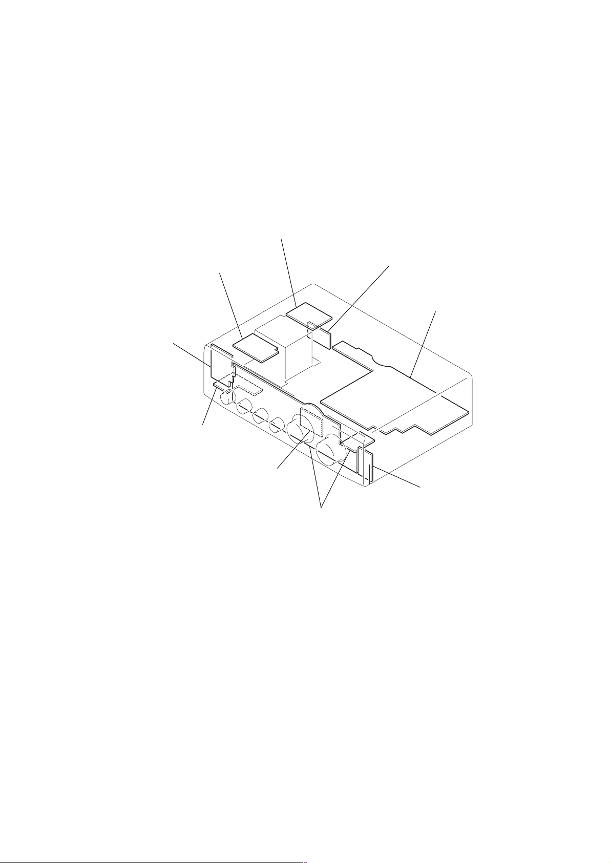
• Circuit Boards Location
SECTION 3
DIAGRAMS
RELAY AC board
RELAY DC board
POWER SW board
HP board
FUNCTION SW board
CONTROL board
AC OUTLET board (AEP)
MAIN board
TAPE MON board (FE520R
)

3-1. NOTE FOR PRINTED WIRING BOARDS AND SCHEMATIC DIAGRAMS
Note on Schematic Diagram:
• All capacitors are in µF unless otherwise noted. pF: µµF
50 WV or less are not indicated except for electrolytics
and tantalums.
• All resistors are in Ω and
specified.
¢
•
: internal component.
1
4
/
W or less unless otherwise
• 2 : nonflammable resistor.
• 5 : fusible resistor.
• C : panel designation.
Note: The components identified by mark ! or dotted line
with mark ! are critical for safety.
Replace only with part number specified.
• U : B+ Line.
• V : B– Line.
• Voltages are dc with respect to ground under no-signal
conditions.
no mark : TUNER
• V oltages are tak en with a V OM (Input impedance 10 MΩ).
Voltage var iations may be noted due to normal production tolerances.
• Signal path.
F : TUNER
E : PB (TAPE1/DAT)
a : REC
d : PB (TAPE2/MD)
J : CD
I : PHONO
Note on Printed Wiring Boards:
• Y : parts extracted from the component side.
¢
•
: internal component.
• b : Pattern from the side which enables seeing.
• Indication of diode
D
This marking side is cathode.
 Loading...