SONY STR-W55 Service Manual
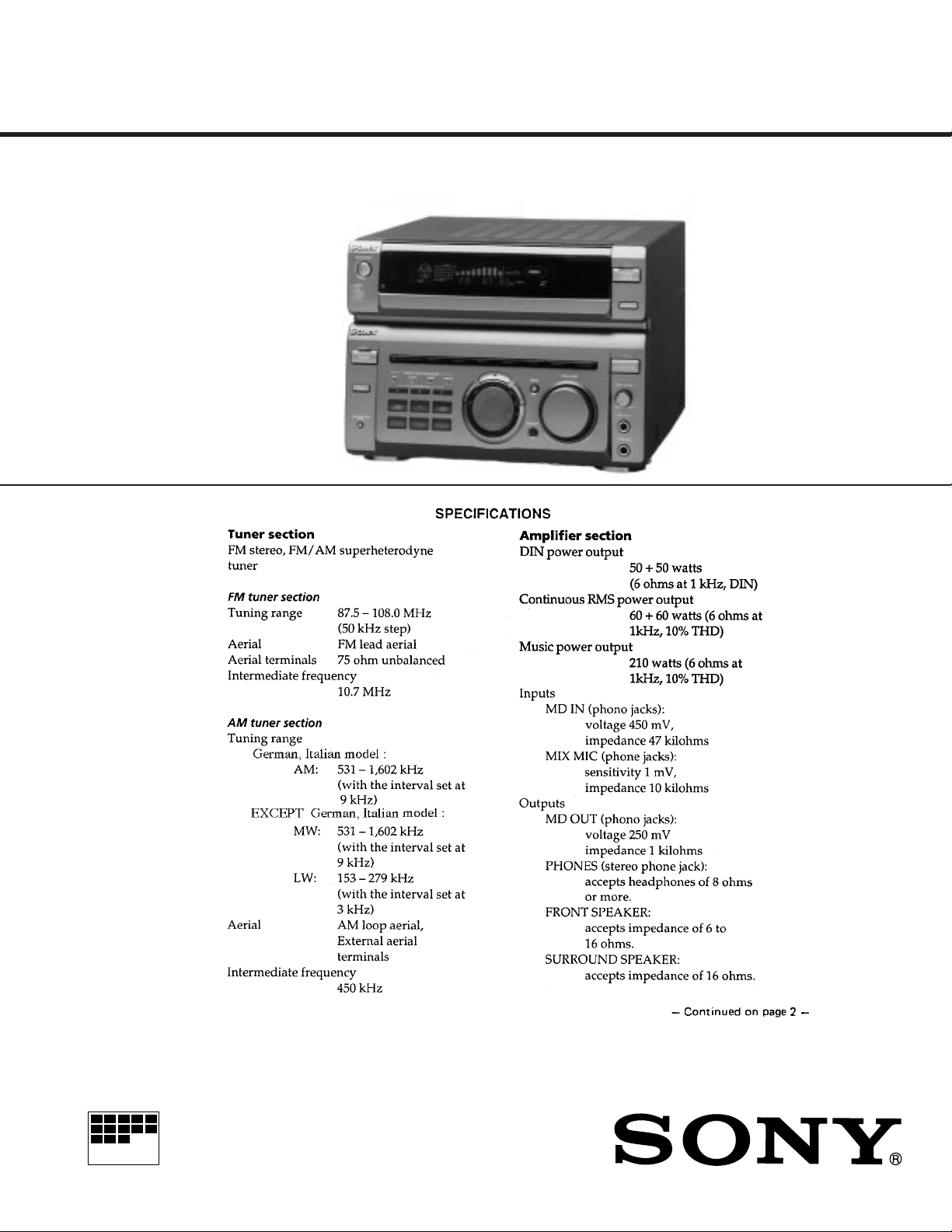
STR-W55
SERVICE MANUAL
STR-W55 is RECEIVER section in
MHC-W55.
AEP Model
UK Model
MICROFILM
FM STEREO/FM-AM RECEIVER
220-230V AC, 50/60Hz (EXCEPT UK)
220-240V AC, 50/60Hz (UK)
TABLE OF CONTENTS
Section Title Page
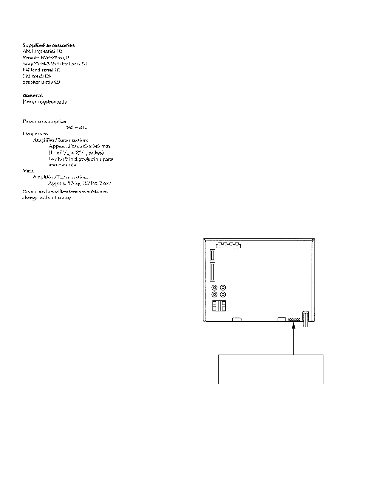
Specifications ...................................................................................1
1. GENERAL ...............................................................................3
2. TEST MODE ........................................................................... 4
3. ELECTRICAL ADJUSTMENTS ..........................................5
4. EXPLANATION OF IC TERMINALS ..................................6
5. DIAGRAMS
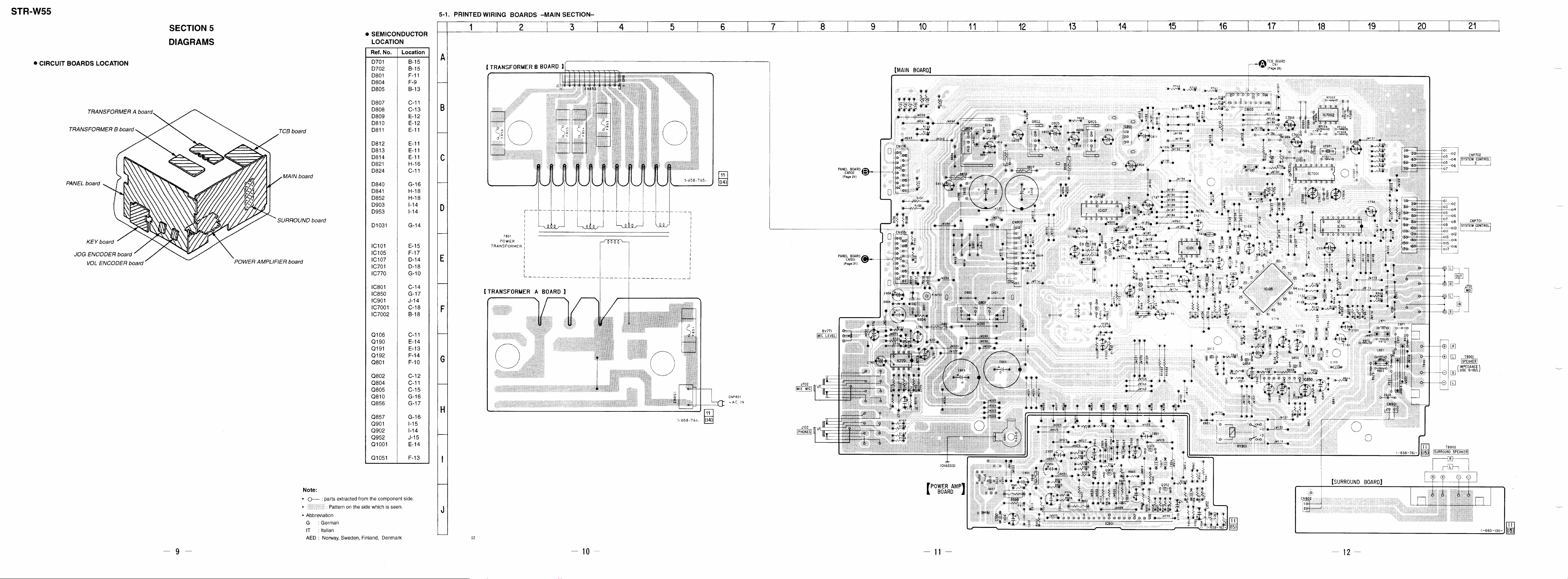
5-1. Printed Wiring Boards – Main Section–..........................10
5-2. Schematic Diagram – Main Section–.............................. 13
5-3. Schematic Diagram – Panel Section– .............................18
5-4. Printed Wiring Boards – Panel Section– .........................21
5-5. Schematic Diagram – TCB Section–...............................23
5-6. Printed Wiring Boards – TCB Section– .......................... 25
6. EXPLODED VIEWS
6-1. Chassis Section................................................................26
6-2. Front Panel Section .........................................................27
7. ELECTRICAL PARTS LIST ...............................................28
Notes on chip component replacement
• Never reuse a disconnected chip component.
• Notice that the minus side of a tantalum capacitor may be damaged
by heat.
SAFETY-RELATED COMPONENT WARNING!!
COMPONENTS IDENTIFIED BY MARK ! OR DOTTED LINE WITH
MARK ! ON THE SCHEMATIC DIA GRAMS AND IN THE PAR TS LIST
ARE CRITICAL TO SAFE OPERATION.
REPLACE THESE COMPONENTS WITH SONY P AR TS WHOSE P ART
NUMBERS APPEAR AS SHOWN IN THIS MANUAL OR IN
SUPPLEMENTS PUBLISHED BY SONY.
MODEL INDENTIFICATION
– BACK PANEL –
Parts No. Model
4-978-033-6π UK
4-978-033-2π AEP, German, Italian, AED
r
Abbreviation
AED : Norway, Sweden, Finland, Denmark
– 2 –
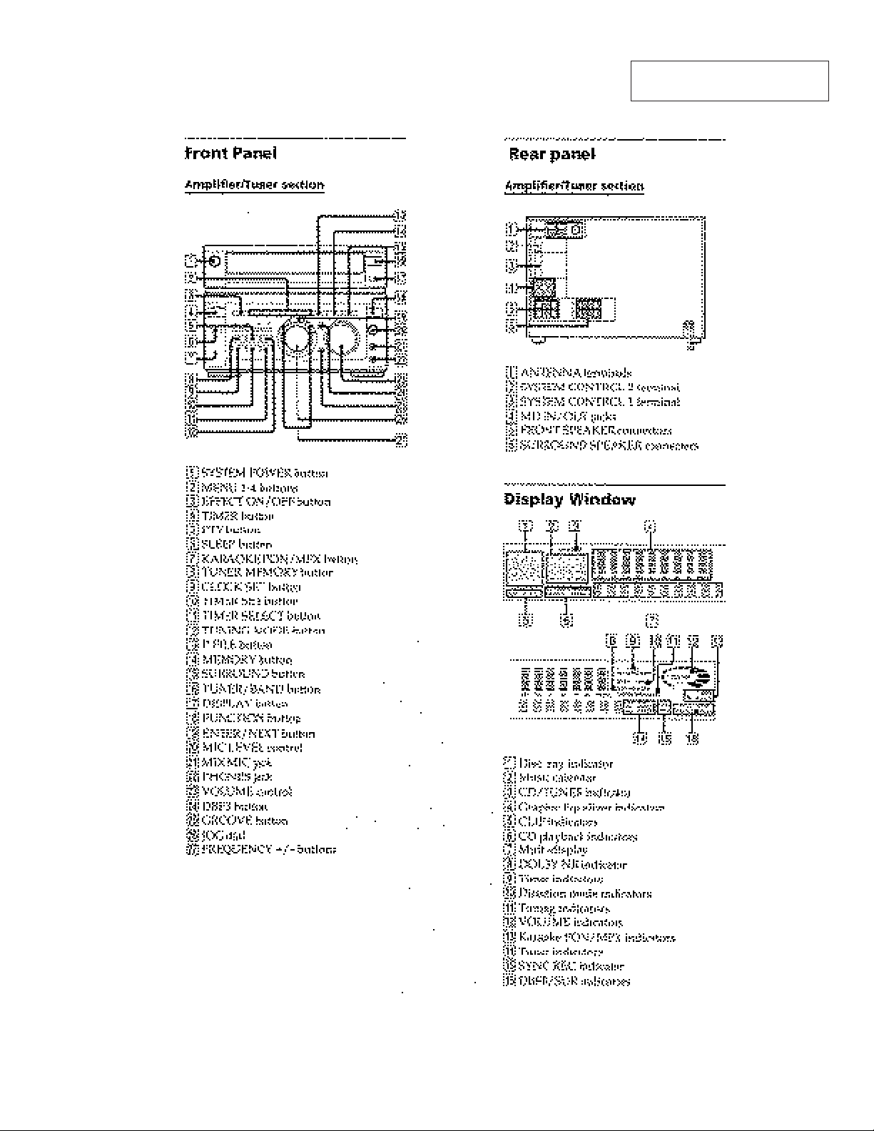
SECTION 1
GENERAL
This section is extracted from
instruction manual.
– 3 –

SECTION 2
TEST MODE
DISPLAY / KEY TEST MODE
Press the ENTER/NEXT and FUNCTION buttons simultaneously.
Then press the MENU 1 button with the following 4 seconds to set the Test Mode.
1. The message “W1 J (destination) ” appears on the screen and a 32 cycle square wave of the subcrystal oscillator is output from Pin 24
(AUB. OUT).
2. Press any key to rotate JOG and all FL indicators light up.
When you rotate JOG at this point, the display changes as follows.
N all FL indicators on Nn FL pattern 1 Nn FL pattern 2 n
The changes and all LED indicators light up.
3. Again press any key to set the key count check. The following display appears.
00 0
The numbers in order from left to right show ; the number of keys pressed, the JOG count (1 click per 4 counts), and the VOL count.
(1 cycle is a count of 96.)
4. Press the Power button to reset to the factory settings.
AMP TEST MODE
Press the ENTER/NEXT and FUNCTION buttons simultaneously.
Then press the MENU 2 button with the following 4 seconds to set the Test Mode.
1. The message “AMP TEST” appears on the screen. Press the MENU button to call up the Equalizer Curve for the Amp Test.
However when the function is set to the tuner, use the MENU button to call up each tuner preset from 1 through 5.
2. Press the Power button to reset to the factory settings.
MICROCOMPUTER COLD START
Press the ENTER/NEXT and FUNCTION buttons simultaneously.
Then press the MENU 3 button with the following 4 seconds to reset the microcomputer to the factory settings.
SUBCRYST AL TEST MODE
Press the ENTER/NEXT and FUNCTION buttons simultaneously.
Then press the MENU 4 button with the following 4 seconds.
The message “XT AL TEST ” appears on the screen and a 32 cycle square w ave of the subcrystal oscillator is output from Pin 24 (A UB.OUT).
In addition, a square wave of the same frequency as the subcrystal oscillator, is output from 4PIN (POWER. ON/OFF).
Press the Power button to reset to the factory settings.
– 4 –
SECTION 3
ELECTRICAL ADJUSTMENTS
Precautions in Repairing
Note. 1 : The adjustment should be performed in the publication.
(AM nFM)
Note. 2 : As a front-end (FE1) is difficult to repair if faulty, replace it
with new one.
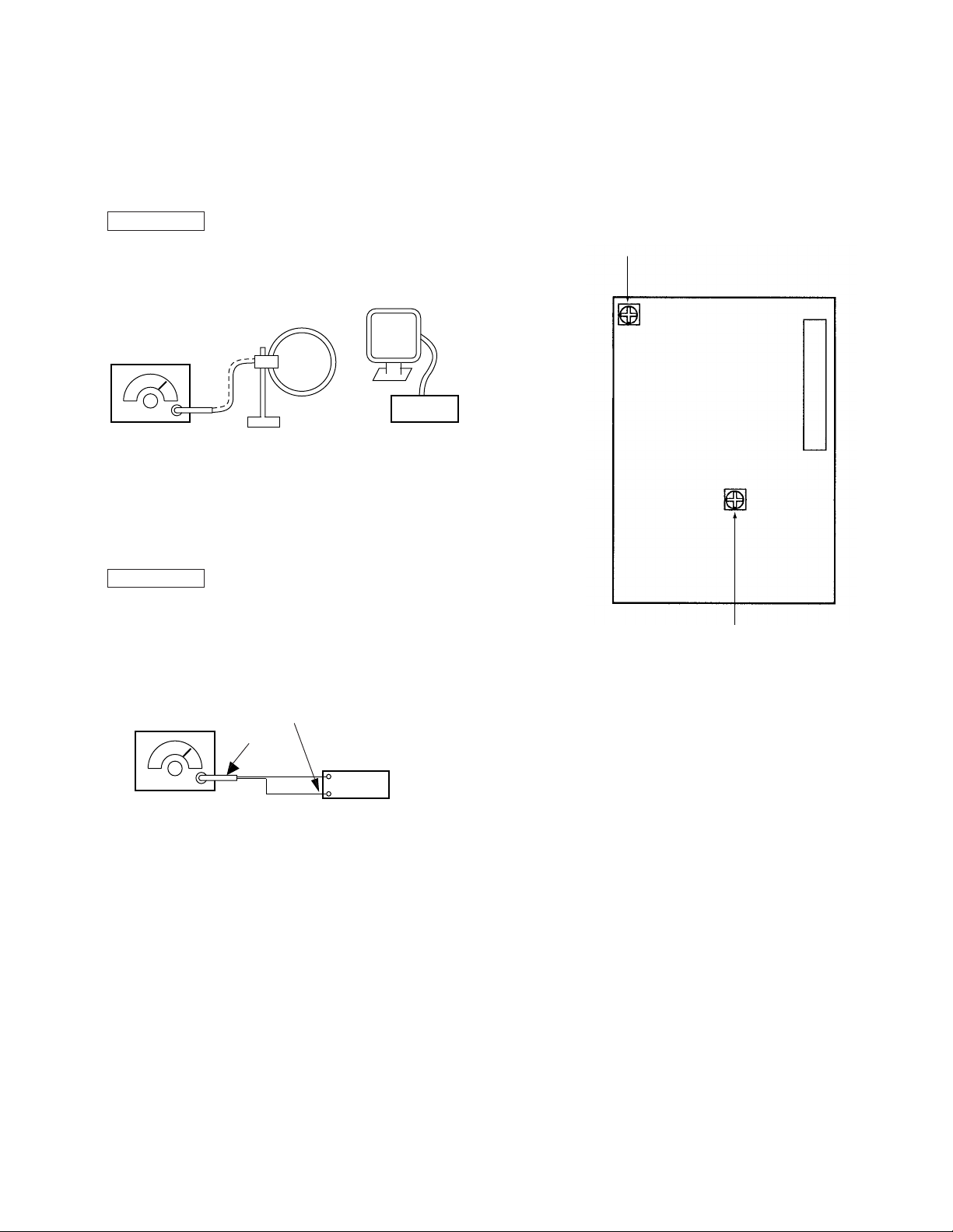
AM SECTION
AM Tuned Indication Lighting Level
Setting :
Band :AM ( MW)
loop antenna B
loop antenna A
AM RF signal
generator
set
Carrier frequency : 999kHz
Procedure :
1. Set loop antenna A so that the loop antenna B input le vel becomes
55dBµ/m (0.6mV/m).
2. Tune the set to 999kHz .
3. Adjust RV41 so that the TUNED indicator goes on.
Adjustment Location :
[ TCB BOARD ] – Component side –
RV41 : AM Tuned Indication Lighting Level
FE1
FM SECTION
FM Tuned Indication Lighting Level
Note : Always make the tuning level adjustment first.
(Since it affects the FM tuning level.)
Setting :
Band : FM
FM RF stereo signal
generator
Carrier frequency : 98MHz
Modulation : OFF
Output level :0.018mV (25dBµ)
FM ANTENNA terminal
75 Ω coaxial
set
Procedure :
1. Tune the set to 98MHz.
2. Adjust RV42 so that the TUNED indicator goes on.
Adjustment Location : TCB board
RV42 : FM Tuned Indication Lighting Level
– 5 –

SECTION 4
EXPLANATION OF IC TERMINALS
IC501 1 ASD0204GF-011-3BA (SYSTEM CONTOROL)
Pin No. Pin name I/O Description
1VDD – Power supply.
2 CLK OUT O Direct output for communications with HCD-W55.
3 RDY IN I/O Direct input / output for communications with HCD-W55.
4 POWER ON / OFF O L : Relay ON
5 MUTE O Mute output to transistor. L : Mute ON
6,7 – – Not used.
8 427LAT O Latch output to IC105 (M62427FP).
9 LED LAT O Latch output to IC504 (M66313FP).
10 RESET I Reset terminal.
11 X2 – Oscillator connection terminal. (5MHz)
12 X1 – Oscillator connection terminal. (5MHz)
13 IC – Ground connection.
14 XT2 – Oscillator connection terminal. (32MHz)
15 XT1 – Oscillator connection terminal. (32MHz)
16 VDD – Power supply.
17 BACK UP I AC Power supply OFF.
18 COM CLK O Transfer clock output serial data.
19 COM DATA O Serial data output.
20 ST DATA IN I Serial data input from IC 1.
21 ST CE O Chip enable output to IC 1.
22 STEREO I Stereo signal input.
23 TUNED I Tuned signal input.
24 AUB OUT O Audio bus output.
25 AVSS – Ground.
26 – – Not used.
27 SUFFIX I Input for model select.
28 SPE I Spectrum analyzer signal input.
29 SPE I Spectrum analyzer signal input.
30 SPE I Spectrum analyzer signal input.
31 SPE I Spectrum analyzer signal input.
32 KYE 1 I Key data input (A/D converter).
33 KYE 2 I Key data input (A/D converter).
34 AVDD – Power supply for anlog.
35 AV REF – Reference voltage for A/D converter.
36 VOL IN A I Volume encoder input.
37 JOG IN A I JOG dial encoder input.
38 RDS CLK I Not uset.
39 AUB IN I Audio bus output.
40 V
SS – Ground.
– 6 –
Pin No. Pin name I/O Description
41 RDS DATA I Not uset.
42 D 3 I/O System control data signal input / output.
43 D 2 I/O System control data signal input / output.
44 D 1 I/O System control data signal input / output.
45 D 0 I/O System control data signal input / output.
46 VDD – Power supply +5V.
47 SIRCS IN I SIRCS signal input.
48 VOL IN B I Volume encoder input.
49 JOG IN B I JOG dial encoder input.
50 ST FM O
51 ST MUTE O
52 EMG OUT O Urgent signal standby output. “H” : standby
53 EMG IN I Urgent signal start input. “H” n “L” : start
57 – 78 P 32 – P 8 O Segment output to FL501.
79 VG – Power supply for fluorescent indicator tube.
80 – 86 P 7 – P 1 O Segment output to FL501.
87 – 100 14 G – 1 G O Grid output for FL501.
BAND select output.
%º pin H L H
%¡ pin L L H
FM Receiving AM Receiving MUTE
– 7 –

– 8 –
 Loading...