Sony STR-DB830, STR-DB930, STR-V929X Service manual
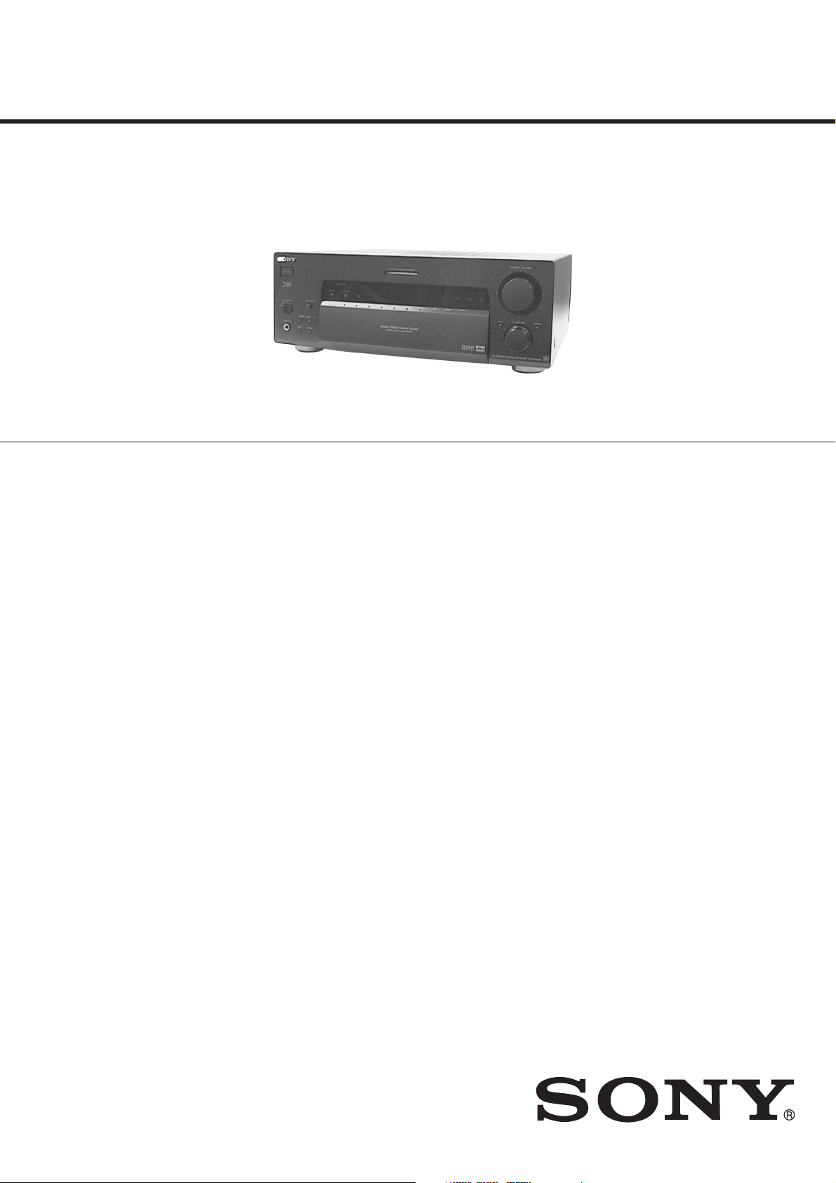
STR-DB830/DB930/V929X
SERVICE MANUAL
Ver 1.1 2002. 02
Photo : STR-DB930 (BLACK model)
Manufactured under license from Dolby Laboratories
Licensing Corporation.
“DOLBY” and the double-D symbol a are trademarks
of Dolby Laboratories Licensing Corporation.
SPECIFICATIONS
AUDIO POWER SPECIFICATIONS
POWER OUTPUT AND TOTAL HARMONIC DISTORTION : With 8
Ω
loads, both channels driven, from 20 - 20,000 Hz ; rated 110 W
(STR-DB930) and 100 W (STR-DB830) per channel minimum
RMS power, with no more than 0.05 % total harmonic distortion
from 250 mW to rated output (USA model only).
Amplifier section
POWER OUTPUT
Stereo mode
North American model
(8 Ω 20 Hz - 20 kHz, THD 0.05 %)
STR-DB930 : 110 W + 110 W
STR-DB830 : 100 W + 100 W
(4 Ω 20 Hz - 20 kHz, THD 0.05 %)
STR-DB930 : 100 W + 100 W
STR-DB830 : 90 W + 90 W
Other model
100 W + 100 W (8 ΩDIN 1kHz)
100 W + 100 W (4 ΩDIN 1kHz)
90 W + 90 W (8 Ω 20Hz-20kHz,thd0.05%)
90 W + 90 W (4 Ω 20Hz-20kHz,thd0.05%)
Surround mode
North American model
(8 Ω 20 Hz - 20 kHz, THD 0.09 %)
STR-DB930 : Front : 110 W + 110 W
STR-DB830 : Front : 100 W + 100 W
(4 Ω 20 Hz - 20 kHz, THD 0.09 %)
STR-DB930 : Front : 100 W + 100 W
STR-DB830 : Front : 90 W + 90 W
Center
Rear
Center
Rear
Center
Rear
Center
Rear
a)
a)
a)
a)
a)
a)
a)
a)
: 110 W
: 110 W + 110 W
: 100 W
: 100 W + 100 W
: 100 W
: 100 W + 100 W
: 90 W
: 90 W + 90 W
US Model
STR-DB930/DB830
Canadian Model
STR-DB930
AEP Model
STR-DB930/DB830
E Model
Australian Model
STR-DB930
Chinese Model
STR-V929X
Other model
(8 Ω 20 Hz - 20 kHz, THD 0.09 %)
Front : 90 W + 90 W
a)
Center
a)
Rear
(4 Ω 20 Hz - 20 kHz, THD 0.05 %)
Front : 90 W + 90 W
Center
a)
Rear
a) Depending on the sound field settings and the source, there may be no
sound output.
Dynamic power output
STR-DB930 : 165 W + 165 W, 8 Ω
STR-DB830 : 155 W + 155 W, 8 Ω
Frequency response
PHONO : RIAA
equalization curve ±0.5 dB
CD, TAPE, MD/DAT, TAPE/MD, DVD/LD, TV/SAT, VIDEO
1,2, andVIDEO3:
10 Hz - 50 kHz + 0.5/-2
dB(with sound field, equalizer, and
Inputs(Analog)
bass boost bypassed)
PHONO :
Sensitivity : 2.5 mV
Impedance : 50 kΩ
S/N
: 90 W
: 90 W + 90 W
a)
: 90 W
: 90 W + 90 W
250 W + 250 W, 4 Ω
240 W + 240 W, 4 Ω
b)
: 86 dB(A, 2.5 mVc))
— Continued on next page —
FM STEREO FM-AM RECEIVER
9-928-896-12
2002B1600-1
© 2002.02
Sony Corporation
Home Audio Company
Published by Sony Engineering Corporation

5.1CH INPUT, CD, DVD/LD, TAPE,
MD/DAT, TAPE/MD, TV/SAT,
VIDEO 1, 2, and VIDEO 3 :
Sensitivity : 150 mV
Impedance : 50 kΩ
b)
S/N
: 96 dB(A, 150 mVc))
b) INPUT SHOR T
c) Weighted network, input level
Input(Digital)
DVD/LD (coaxial) :
Sensitivity : Impedance : 75 Ω
S/N : 100 dB(A, 20 kHz LPF)
DVD/LD, TV/SAT, MD/DAT (Optical)
Sensitivity : Impedance : S/N : 100 dB(A, 20 kHz LPF)
Outputs TAPE, MD/DAT, TAPE/MD, (REC OUT)
; VUDEO 1, 2 (AUDIO OUT) :
Voltage : 150 mV
Impedance : 10 kΩ
FRONT L/R, CENTER, REAR L/R, SUB
WOOFER :
Voltage : 2V
Impedance : 1 kΩ
PHONES :
Accepts low-and high-impedance headphones
BASS BOOST +6 dB at 70 Hz
Sampling Frequency 48 kHz
EQ BASS : 100 Hz - 1.0 kHz(21 steps)
MID : 500 Hz - 5.0 kHz(21 steps)
TREBLE : 1.0 kHz - 10 kHz(21 steps)
Gain levels : ±10 dB, 1 dB step
FM tuner section
Tuning range 87.5 - 108.0 Hz
Antenna terminals
75 Ω, unbalanced
Sensitivity Mono : 18.3 dBf, 2.2 µV/75 Ω
Stereo : 38.3 dBf, 22.5 µV/75 Ω
Usable sensitivity
11.2 dBf, 1 µV/75 Ω
S/N Mono : 76 dB
Stereo : 70 dB
Harmonic distortion at 1 kHz
Mono : 0.3 %
Stereo : 0.5 %
Separation 45 dB at 1 kHz
Frequency response 30 Hz - 15 kHz +0.5/-2 dB
Sencitivity 60 dB at 400 kHz
AM tuner section
North American and E models
With 10-kHz tuning scale : 530 - 1,710 kHz
With 9-kHz tuning scale : 531 - 1,710 kHz
d)
d)
Other models
531 - 1,602 kHz
Antenna Loop antenna
Usable sensitivity
50 dB/m(at 1,000 kHz or 999 kHz)
S/N 54 dB(at 50 mV/m)
Hermonic distortion
0.5 %(50 mV/m, 400 kHz)
Selectivity At 9 kHz : 35 dB
At 10 kHz : 40 dB
d) You can change the AM tuning scale to 9kHz. After tuning in any AM
station, turn off the receiver. Hold down the TUNING + button and press
the 1/u button. All preset stations will be erased when you change the
tuning scale. To reset the scale to 10 kHz, repeat the procedure.
Video section
Inputs V ideo : 1 Vp-p 75 Ω
S-video : Y : 1 Vp-p 75 Ω
C : 0.286 Vp-p 75 Ω
Outputs Video : 1 Vp-p 75 Ω
S-video : Y : 1 Vp-p 75 Ω
C : 0.286 Vp-p 75 Ω
General
System Tuner section :
PLL quarts-locked digital synthesizer system
Preamplifier section :
Low-noise NF type equalizer
Power amplifier section :
Pure-complementary SEPP
Power requirements
USA, Canadian models
120V AC, 60Hz
Australian model
240V AC, 50Hz
Other model
220 – 230V AC 50/60Hz
Power consumption
STR-DB930
Canadian :400 V A
Other models :290 W
STR-DB830
North American models : 280 W
AC outlets
North American models : 2 switched, total 120 W/1A
Other models : 1 switched, max 100 W
Dimensions 430 × 405 × 160.5 mm
(17 × 16 × 63/8 in.)
including projecting parts and controls
Mass(Approx.)
13 kg(28 lb 11oz)
Supplied accessories
• FM wire antenna (1)
• AM loop antenna (1)
• Audio/video/control S connecting cord (1)
• CONTROL A1 connecting cord (1)
• FM antenna adapter (1)
STR-DB930, V929X only
• Remote commander RM-LJ302 (remote) (1)
• LR6 (size-AA) alkaline batteries (3)
STR-DB830 only
• Remote commander RM-PP402 (remote) (1)
• LR6 (size-AA) batteries (2)
Design and specifications are subject to change without notice.
MODEL IDENTIFICATION
– BACK PANEL –
PART NO.
MODEL
DB930: US model
DB930: Canadian model
DB930: Malaysia, Singapore models
V929X
DB930: Australian model
DB930: AEP model
DB830: US model
DB830: AEP model
— 2 —
PARTS No.
4-217-716-0π
4-217-716-1π
4-217-716-2π
4-217-716-3π
4-217-716-4π
4-217-716-5π
4-217-716-6π
4-217-716-7π
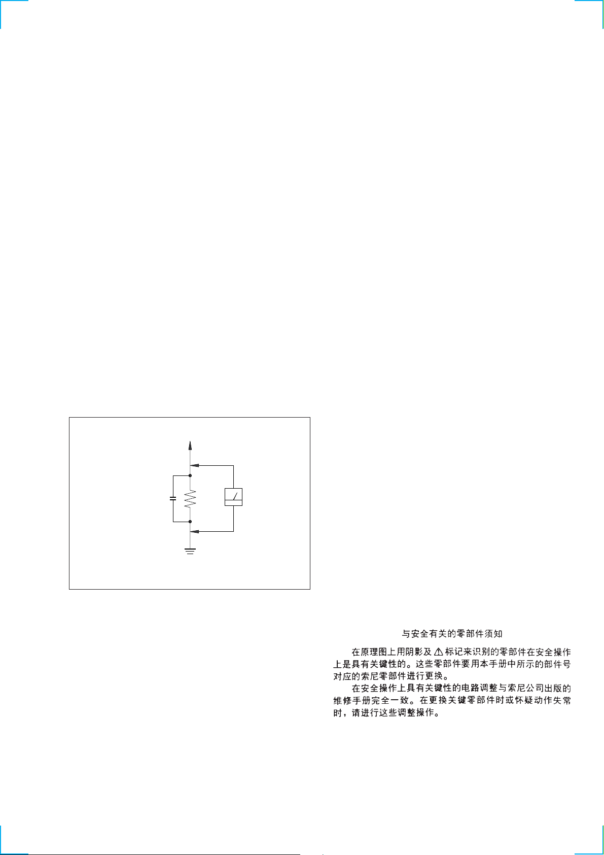
TABLE OF CONTENTS
SAFETY CHECK-OUT
(US model only)
After correcting the original service problem, perform the
following safety checks before releasing the set to the customer:
Check the antenna terminals, metal trim, “metallized” knobs, screws,
and all other exposed metal parts for AC leakage. Check leakage as
described below.
LEAKAGE
The AC leakage from any exposed metal part to earth ground
and from all exposed metal parts to any exposed metal part having
a return to chassis, must not exceed 0.5 mA (500 microampers).
Leakage current can be measured by any one of three methods.
1. A commercial leakage tester, such as the Simpson 229 or RCA
WT -540A. Follow the manufacturers’ instructions to use these
instruments.
2. A battery-operated AC milliammeter. The Data Precision 245
digital multimeter is suitable for this job.
3. Measuring the voltage drop across a resistor by means of a
VOM or battery-operated AC voltmeter . The “limit” indication
is 0.75 V, so analog meters must have an accurate low-voltage
scale. The Simpson 250 and Sanwa SH-63Trd are examples of
a passive VOM that is suitable. Nearly all battery operated
digital multimeters that have a 2V AC range are suitable. (See
Fig. A)
1. GENERAL ·········································································· 4
2. SERVICEING NOTE ······················································· 6
3. TEST MODE······································································ 6
4. DIAGRAMS
4-1. Block Diagram Main Section ··········································· 7
4-2. Block Diagram Power Section ········································· 9
4-3. Circuit Board Location····················································· 11
4-4. Schematic Diagram Digital Section(1/3) ······················· 13
4-5. Schematic Diagram Digital Section(2/3) ······················· 15
4-6. Schematic Diagram Digital Section(3/3) ······················· 17
4-7. Printed Wiring Board Digital Section(1/2)·····················19
4-8. Printed Wiring Board Digital Section(2/2)·····················21
4-9. Printed Wiring Board Display Section ··························· 23
4-10. Schematic Diagram Display Section ······························ 25
4-11. Printed Wiring Board Speaker Switch Section··············· 27
4-12. Schematic Diagram Speaker Switch Section ·················29
4-13. Printed Wiring Board Rear AMP Section ······················· 31
4-14. Schematic Diagram Rear AMP Section ························· 33
4-15. Printed Wiring Board Power Section ····························· 35
4-16. Schematic Diagram Power Section ································ 37
4-17. Printed Wiring Board Video Section ······························ 39
4-18. Schematic Diagram Video Section································· 41
4-19. Printed Wiring Board Main Section ······························· 43
4-20. Schematic Diagram Main Section(1/2) ·························· 45
4-21. Schematic Diagram Main Section(2/2) ·························· 47
4-22. IC Pin Function ································································ 49
4-23. IC Block Diagrams ··························································· 58
To Exposed Metal
Parts on Set
AC
0.15µF
1.5k
Ω
voltmeter
(0.75V)
Earth Ground
Fig. A. Using an AC voltmeter to check AC leakage.
5. EXPLODED VIEWS
5-1. Front Panel Section ·························································· 62
5-2. Chassis Section································································· 64
6. ELECTRICAL PARTS LIST ······································· 66
SAFETY-RELATED COMPONENT WARNING!!
COMPONENTS IDENTIFIED BY MARK ! OR DOTTED LINE WITH
MARK ! ON THE SCHEMATIC DIAGRAMS AND IN THE PARTS
LIST ARE CRITICAL TO SAFE OPERATION. REPLACE THESE
COMPONENTS WITH SONY PARTS WHOSE PART NUMBERS
APPEAR AS SHOWN IN THIS MANUAL OR IN SUPPLEMENTS
PUBLISHED BY SONY .
— 3 —
ATTENTION AU COMPOSANT AYANT RAPPORT
À LA SÉCURITÉ!
LES COMPOSANTS IDENTIFÉS P AR UNE MARQUE ! SUR LES
DIAGRAMMES SCHÉMA TIQUES ET LA LISTE DES PIÈCES SONT
CRITIQUES POUR LA SÉCURITÉ DE FONCTIONNEMENT. NE
REMPLACER CES COMPOSANTS QUE PAR DES PIÈSES SONY
DONT LES NUMÉROS SONT DONNÉS DANS CE MANUEL OU
DANS LES SUPPÉMENTS PUBLIÉS PAR SONY.
Identifying the Parts
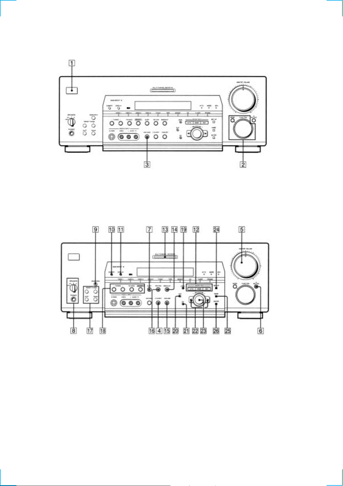
Front Panel
1 1/u switch
2 FUNCTION control
3 INPUT MODE button
SECTION 1
GENERAL
MODE button
4 5.1CH INPUT button
5 MASTER VOLUME control
6 MUTING button
7 SLEEP button (EXCEPT AEP)
RDS PTY button (AEP model)
8 SPEAKERS selector
PHONES jack
9 DOOR OPEN button
0 DIMMER button
!¡ DISPLAY button
!™ A.F.D button/indicator
MODE button/indicator
2CH button/indicator
!£ MULTI CHANNEL DECODING indicator
!¢ BASS BOOST button
!∞ EQUALIZER button
— 4 —
!§ TEST TONE button (EXCEPT AEP)
RDS EON button (AEP model)
!¶ PRESET TUNING +/- buttons
SHIFT button
FM/AM button
!• TUNNIG +/- buttons
FM MODE button
MEMORY button
!ª LEVEL button
@º SUR button
@¡ EQ button
@™ Cursor buttons (</>)
@£ Jog dial
@¢ SET UP button
@∞ NAME button
@§ ENTER button
SECTION 2
SERVICING NOTE
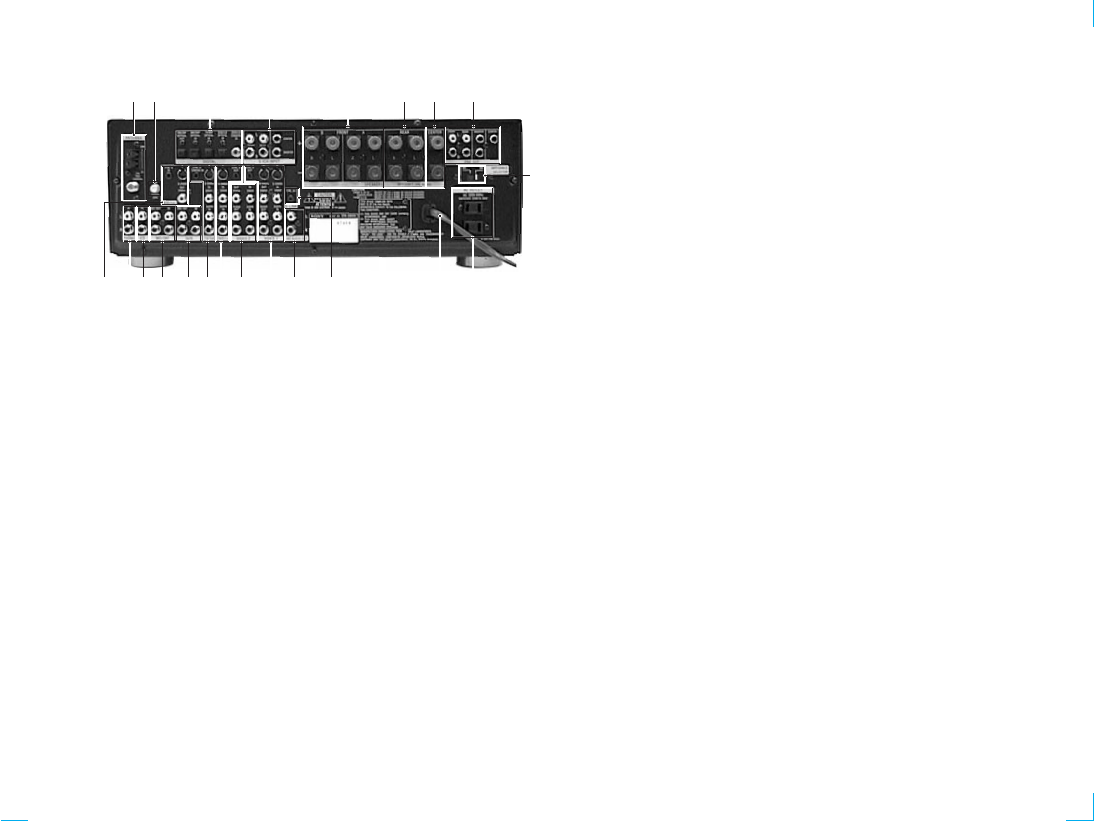
Rear Panel
1 2
3
1 ANTENNA
2 SIGNAL GND
3 DIGITAL
4 5-1 CH INPUT
5 SPEAKERS (FRONT)
6 SPEAKERS (REAR)
7 SPEAKERS (CENTER)
8 PREOUT
9 IMPEDANCE SELECTOR
!º AC OUTLET
!¡ AC power cord
4 5 6 7 8
!™!£!¢!∞!§!¶!•!ª@º@¡@™
!™ S-LINK
!£ 2ND AUDIO OUT
!¢ VIDEO 1
!∞ VIDEO 2
!§ DVD/LD
!¶ TV/SAT
!• TAPE
!ª MD/DAT
@º CD
@¡ PHONO
@™ MONITOR
1. When the front panel is removed, the VR board is removed at the
same time. Consequently the LEDs cannot be turned on and the
sound volume cannot be increased or decreased from the remote
control.
2. When servicing the DIGIT AL board, be sure to connect the earth
land of the DIGITAL board with the chassis frame so that the
earth potential of the DIGITAL board must not be floated from
the chassis frame.
SECTION 3
TEST MODE
9
0!¡
FLUORESCENT INDICATOR TUBE TEST MODE
* All fluorescent segments are tested. When this test is activated,
all segments turn on at the same time, then each segment turns on
one after another.
* Procedure:
While depressing the ENTER, the LEVEL and the EQ buttons
simultaneously, press the power [1/u] button to turn on the main
power. All segments turn on at the same time, then each segment
turns on press the ENTER button.
FACTORY SET MODE
* All preset contents are reset to the default setting.
* Procedure:
While depressing the SET UP, the LEVEL and the ENTER buttons
simultaneously, press the power [1/u] button to turn on the main
power. The message Factry Set appears and the present contents
are reset to the default values.
ALL CLEAR MODE
* All preset contents are cleared when this mode is activated. Use
this mode before returning the product to clients upon completion
of repair.
* Procedure:
While depressing the SET UP button simultaneously, press the
power [1/u] button to turn on the main power. The machine enters
the DEMO mode.DEMO mode: Wait a while, then the
demonstration starts. If the power [1/u] button is pressed often
the demonstration has started, the power is turned off, and the
demonstration resumes if the power [1/u] button is pressed again.
ALL CLEAR mode; If the power [1/u] button is pressed often
the machine enters the DEMO mode, but before the demonstration
starts, the display is turned off. Press [1/u] again. No response is
returned. The press [1/u] again. The preset data is cleared and
the machine enters the normal power-on state.
SOUND FIELD CLEAR MODE
* The preset sound field is cleared when this mode is activated.
Use this mode before returning the product to clients upon
completion of repair.
* Procedure:
While depressing the SOUND FIELD MODE button, press the
power [1/u] button to turn on the main power. The message S.F
Initialize appears and initialization is performed.
AM CHANNEL STEP 9 kHz/10 kHz
SELECTION MODE (US,Canadian Model)
* Either the 9 kHz step or 10 kHz step can be selected for the AM
channel step.
* Procedure:
Set the FUNCTION to AM. Turn off the main power.
While depressing the TUNING+ button or the PRESET TUNING
+ button, press the power [1/u] button to turn on the main power.
Either the message AM 9kHz Step or AM 10kHz Step appears.
Select the desired step.
DSP TEST MODE
* It tests whether the DSP works correctly or not. When the DSP
test is activated, the test data is output from the DSP (IC1401:
CXD2712R) of the DIGITAL board and is written in the RAM
(IC1402: IDT71V016S). When the test data is read from the RAM
by the DSP, the data output must be equivalent to the original
data. If they disagree, an error is triggered. Errors can be caused
by the broken data line or defective soldering.
* Procedure
While pressing the SETUP, LEVEL and SUR buttons, press the
POWER button to enter the DSP test mode. The message DSP
TEST MODE appears. When an error occurs, the message DSP2
ERROR is displayed. When there is no error, the message DSP2
NO ERROR appears and the 1 kHz signal is output to all channels.
Then, the mode can be switched the (SIGN W AVE) (THROUGH)
and (INPULSE) mode.
AUTOBETICAL MODE (AEP Model only)
* This mode is installed in the Europe models only . When this mode
is used, the receiver scans the broadcasts that can be received by
tuner, and sets up the broadcasts. Be sure to start scanning after
connecting the antenna.
Procedure:
Check that the antenna is connected. Press the POWER button
while pressing the MEMORY button to turn on the power. The
message “Autobetical select” appears and scanning starts by tuner.
VERSION MODE
* When this mode is used, the microprocessor version number is
displayed.
* Procedure:
Press the POWER button while pressing the ENTER, LEVEL,
and SUR buttons to turn on the power. The microprocessor version
number appears as follows.
— 5 — — 6 —
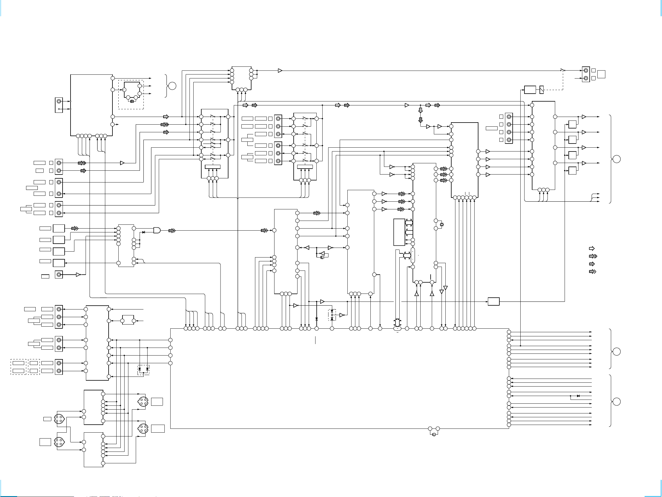
STR-DB830/DB930/V929X
4-1. BLOCK DIAGRAM MAIN SECTION
US,CANADIAN
MODEL
TV/DBS
DVD/LD
TAPE (MD)
MONITOR
DAT/MD
VIDEO 1
VIDEO 2
MODEL
TV/LD
TUNER UNIT
TM301
ANTENNA
FM
75Ω
AM
L
PHONO
LCD
LINPUT
LOUTPUT
L
INPUT
LOUTPUT
DVD/LD
TV/DBS
DAT/MD
(INPUT)
MD/DAT
(REC OYT)
COAXIAL
DVD
OUTPUT
INPUT
OUTPUT
INPUT
OUTPUT
AEP
INPUT
DVD
INPUT
Y
J253
DVD
C
J252
Y
VIDEO 1
INPUT
C
J301
J302
J303
IC001
IR LINK
DET
IC002
IR LINK
DET
IC003
IR LINK
DET
IC004
IR LINK
DET
J001
J201
J202
J203
FM
AM
DO
4 14 15 13 2 3 1
DO
IC007
16
TUNED
TUNED
5
13
5
STEREO
STEREO
1
13
15
9
11
3
5
V1 I
LD
V1 I
M OUT
V1 IN
V1 OUT
V2 IN
V2 OUT
TV
LD
Y SWITCH
C SWITCH
T. MUTE
S DATA
MUTING
VIDEO SELECT
IC201
IC252
V1 O
IC251
V1 O1315
M O
ANT LEVEL
L OUT
R OUT
DATA
CLK
S CLK
VCC
VEE
SW1
SW2
SW3
SW4
SW5
15
14SW1
10SW2
4SW3
6SW4
1LDM O
14SW1
10SW2
4SW3
6SW4
1
6
9FM DET
10
12
CE
S LAT
16
8
14
10
4
6
2
R CH
EQ AMP
IC302
5
4
6
SWITCH
3
4
9
3 2
SECTION 4
DIAGRAMS
2
RDS
IC1
4
16
13 14
X1
4.33MHz
AEP ONLY
7
SELECT
10
IC1005
11
12
A
14
A
B
2
B
IC202
-5V
REG
SELECTOR
IC330
26
COM
TUNER
CD
MD
TAPE
S DATA
S DATA
47
S CLK
S CLK
48
EV DATA
COM
COM
161415
S LAT
DVD/LD
VIDEO2
VIDEO1
S LAT
EV CLK46EV STB
23
20
17
112
DI
INPUT
INPUT
OUTPUT
110CL111CE115
ANT LEVEL
RDS DATA
RDS CLK
+5V
-15V
IC1006
A
VIDEO(SW1)77
VIDEO(SW2)76
VIDEO(SW3)
75
72
VIDEO(SW4)
DO
58
TUNED
59
DATA
TMUTE
STEREO
60
84
STEREO
AUTO STOP
4
3
2
8
6
11
10
S DATA
56
DATA
TUNER MUTE
AUDIO SELECT
IC301
CONTROL
CLK
14DI15
S DATA
S CLK
S LAT
S CLK
57
CLOCK55LATCH
27
25
23
5
9
12
CE
16
S LAT
A
B
108
107
DIG IN A
DIG IN B
D201
Y
VIDEO 1
OUTPUT
C
Y
J251
MONITOR
OUTPUT
C
LTV/DBS
L
LOUTPUT
LINPUT
L
LINPUT
BY SYNC
IC309
J305
J304
DIGITAL AUDIO
3
D IN
36
DI
38
CLK
37
CE
33
BP SYNC
I/F RECEIVER
IC1101
CK OUT
12.288M
ERROR
CSFLAG
XMODE
48
25
109
117
118
XMODE
CSFLAG
Q301
RY301
RELAY
DRIVE
SELECTOR
IC1502
19
SELECTOR
IC303
27
26
25
24
22
21
DATA
16
13
BCK
14
LRCK
15
22
34
DO
35
AUTO
32
XSTAT E
17
Q1102
XSTAT E
CONTROL
14DI15
S DATA
IC11404
116
113
AUTO
CLK
S CLK
23
20
17
CE
16
S LAT
IC1404
IC1404
X3501
12.288MHz
Q1204
Q1203
D1203
D1202
106
ANALOG/DIG
85
S MUTE
S MUTE
SYSTEM
CONTROL
114
DO
ERROR
DIGITAL AUDIO DECODER
84
SDIA0
85
SDIA1
83
SDBCK0
82
SDWCK0
8
XI
SCK
69
1
SCCLK
IC201
DOLBY
IC1301
AUDATA0
AUDATA1
AUDATA2
SI
68CS66IC62
2SI4CS5
24
23
22
SO
67
3
IC
SO
IC1403
IC1403
IC1403
IC1403
IC1403
SRAM
IC1402
D0-7
24 17
HD0 HD7
IC304
D0-7
J1002
AUDIO CODEC
HRDY
X1401
10MHz
15
SOD
30
29
9
39
4
5
6
7
8
Q1202
LIN+
LIN-
SDTO
MCLK1
BCLK
LRCK
SDTI 1
SDTI 2
SDTI 3
CDTO
44
30
CDTI
IC1503
43
31
CDTI
42CS41PD17
29
CDTO
CCLK
CCLK
28CS32
L OUT1
L OUT3
R OUT3
L OUT2
27
23
24
25
DFS
11
35
PD
96kHZ
IC1504 IC1504
AUDIO DSP
IC1401
113
BCK0
SOA
14
16
XHDCS
XHDCS
CLKO
HRDY
SOB
SOC
CLKI
SOD
26
IC1202
26
XI
X1201
16MHz
XRST
XRST
2
3
4
99
100
5
13
Q1201
27
92XO93
114
BCK1
115
LRCK0
116
LRCK1
117
SIA
118
SIB
119
SIC
D0-7
A0-7
74
XWE
70
XOE
16
20
HD0
.
23
HD7
25
15
HA0
XHDWR
9
IC1202
13
25
HA0
XHDWR
L
LS
5.1 INPUT
C
W
IC1507
IC1505
IC1505
IC1506
Q1507
MUTE
CONT
RY PRE PRE RY
98
AC MUTE
82
PROTECT
66
RY HP
104
RY FRONT A
99
RY FRONT B
100
RY CENTER
101
RY WOOFER
103
RY REAR
102
50
DISP DATA
52
DISP CLK
DISP MR
49
SREQ
51
90RESET
105RY POWER
67STOP
10
SOTO
9
SINO
87
MD2
89
MD0
2CH L
20
L OUT
S.1-L
23
S.1-LS
26
S.1-C
3
S.1-C
21
L
27
C
2
W
24
LS
17
C OUT
25
W OUT
4
22LS OUT
161415
S DATA
S CLK
S LAT
R CH
MUTE
Q1502
MUTE
Q1506
MUTE
Q1505
MUTE
Q1504
D1201
IC1510
IC1508
IC1508
IC1509
J306
L
AUDIO
OUT
R
DATA
CLK
LAT
• RCH is omitted
• Signal Path
: FM
: PHONO
: CD
: DVD
AC MUTE
PROTECTOR
HP RY
SP/A RY
SP/B RY
RY CENTER
RY WOOFER
REAR SP RY
U DATA
U CLOCK
U MREQ
U SREQ
U REST
RESET
RY POWER
STOP
SOT0
SIN1
MD2
MD0
L
C
W
B
SL
C
D
— 7 — — 8 —
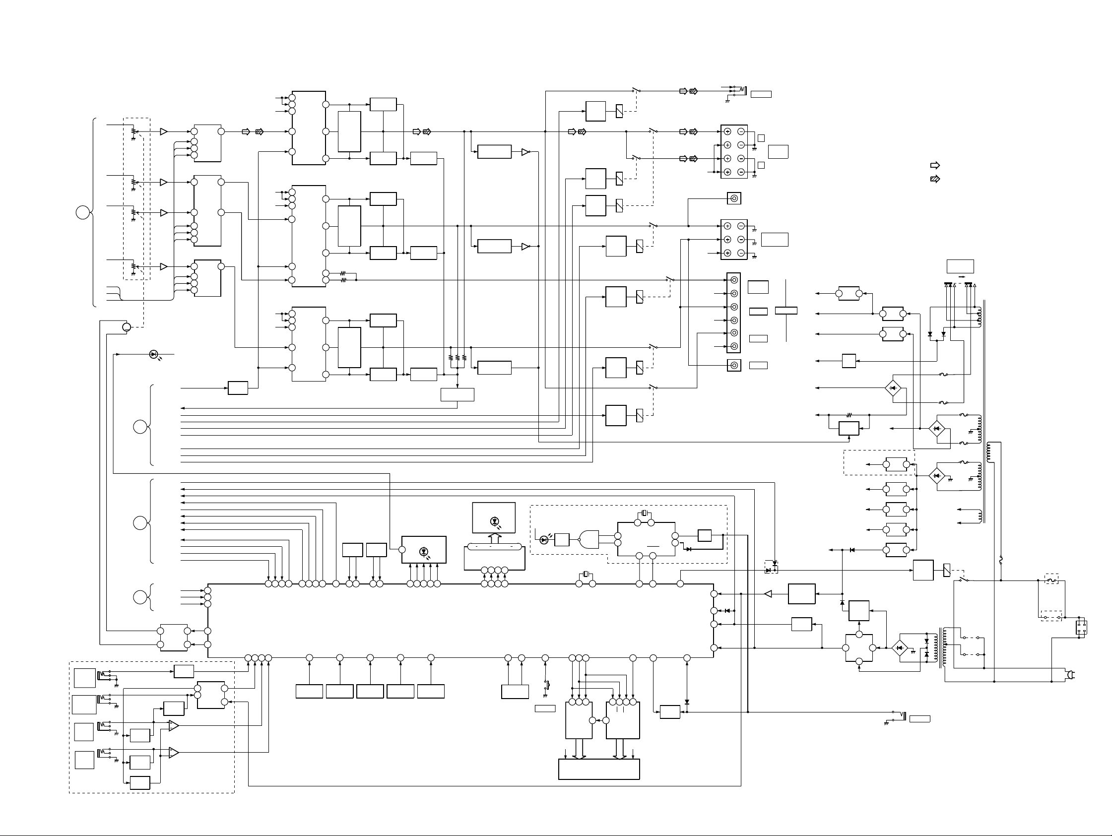
STR-DB830/DB930/V929X
Ver 1.1 2002. 02
4-2. BLOCK DIAGRAM POWER SECTION
VOLUME
W
B
SL
DATA
CLK
LAT
US,Canadian MODEL
J258
TV/SAT
CONTL S
STATUS IN
J257
MONITOR
CONTROL S
IN
J255
VIDEO 1
CONTL S
OUT
J256
DVD/LD
CONTL S
OUT
RV401
L
C
IC408
IC410
IC410
IC409
M
AC MUTE
PROTECTOR
PRE RY
RY HP
SP/A RY
C
SP/B RY
RY CENTER
RY WOOFER
RY REAR
RY POWER
STOP
RESET
URESET
USREQ
UMREQ
UCLOCK
D
UDATA
FLASH DO
FLASH DI
RDS DATA
RDS CLK
A
ANT LEVEL
2
MOTOR
4
Q251,252
SWITCH
3
LEVEL
LEVEL
Q254
LEVEL
2
5
6
Q255,256
CONTROL
Q257,258
CONTROL
CONTROL
MD2
MD0
IC103
DRIVE
IC254
IC254
DATA
CLK
LAT
DATA
CLK
LAT
DATA
CLK
LAT
BUFFER
Q253
1
7
8
5
VOL CONT
14
IN
9
DATA
8
CLK
10
LAT
VOL CONT
3
IN
IN1415
9
DATA
8
CLK
10
LAT
VOL CONT
14
IN
9
DATA
8
CLK
10
LAT
9
11
IC414
IC416
IC415
54
53
46
55
56
ST-I/O
IC253
OUT
15
OUT
OUT
OUT
15
RDS DATA
RDS CLK
RDS SIGNAL
UP
DOWN
2
MUTE
Q501,503
MBUS TV
96
95
6
4
+VDD
-VDD
+VDD
-VDD
+VDD
-VDD
49
MBUS STA OUT
MBUS VIDEO 1
94
93
51
20
MD0
MD2
MBUS DVD
POWER AMP(L)
13 VCC
VCC
14
VEE
15
6
IN
1
MUT
POWER AMP(C/W)
13 VCC
14 VCC
VEE
15
IN
8
1 MUT
IN
6
POWER AMP(SL)
13 VCC
VCC
14
VEE
15
IN
6
MUT
1
19
SINO
SOTO
IC501
IC601
IC701
61
62
UDATA
38
FUNCTION
KEY
S126-128
+VE
NF
-VE
12
+VE
NF
11
-VE
+VE
NF
-VE
60
58
UMREQ
URESET
UCLOCK
KEY INPUT 1
2
5
3
9
2+VE
3-VE
2
5
3
Q504, Q505
Q604, Q605
Q704, Q705
59
USREQ
39
FUNCTION
KEY
S119-121
S131
BIAS
BIAS
BIAS
RV101
79
78
FUNCTION UP
KEY INPUT 2
BOOSTER
Q506
BOOSTER
Q507
BOOSTER
Q606
BOOSTER
Q607
BOOSTER
Q706
BOOSTER
Q707
RV102
76
75
JOG UP
FUNCTION DOWN
KEY INPUT 3
40
FUNCTION
KEY
S115-118
S129,130
JOG DOWN
FUNCTION
S111-114
S122-124
29
KEY INPUT 4
41
KEY
CUR DET
Q598
CUR DET
Q698
CUR DET
Q798
D140-145
21 543
PHONO
TUNER
CD
MD/DAT
MODE CONTROL
KEY INPUT 5
43
FUNCTION
KEY
S103-110
TAPE
IC102
PROTECTOR
Q547-549
AF DETECTOR
Q509,510
AF DETECTOR
Q609,610
AF DETECTOR
Q709,710
D122,123,136-140
D147,149-157
..
915 20 2917
LED DRIVER
IC108
89
87
88
LED CE
LED CLK
LED DATA
19181716
90
LED CLR
64
SPEAKER
SP A
SWITCH
S102
65
Q511
Q611
SP B
DB930/V929 MODEL
+B
D124,125,128
POWER KEY
66
S101
POWER
Q129,130
SIRCS
DET.
IC107
X101
16MHz
82
XO
FL CLK
FL LAT
FL CLEAR
21
24
25
26
34
LAT
CLK24CLR
DIN
FL DRIVE FL DRIVE
F2
FLOURESCENT
INDICATOR TUBE
RELAY
DRIVE
Q601
RELAY
DRIVE
Q546
RELAY
DRIVE
Q596
83
29
XI
FL101
R CH
RY602
RY501
RY502
RY601
RELAY
DRIVE
Q645
RY681
RELAY
DRIVE
Q681
RY701
RELAY
DRIVE
Q745
RY671
RELAY
DRIVE
Q671
IC106
SIRCS
CARR OUT
2
SIRCS IN
33
4LS29
5CL30
CLK
3
DOUT
IC105IC104
X102
7.82MHz
16
15
XI
XO
CA1 I
CA1 O
RESET
LAT
14
5
99
98
LAT
RESET
FL DAT
ABUS OUT
22
67
DIN
F1
Q104
BUFFER
R CH
R CH
R CH
R CH
R CH
Q105
CTL
11
12
I/O
7
POWER RY
ABUS A1 IN
63
SIRCS
URESET
RESET
STOP
I/O
26
58
77
47
J701
PHONES
L
A
L
R
L
R
L
R
JJ101
SUB
WOOFER
REAR
FRONT
JJ102
CENTER
B
SURROUND
D1209
Q101
TM501
FRONT
SPEAKER
TM701
SPEAKER
PRE OUT
+5V
+15V
-15V
+32V
+VDD
-VDD
DISP µCOM+5.6V
IC101
REMOTO
CONTROL
RECEIVER
RESET
Q103
DIGITAL PWB
FROM SUFFIX-12
D1211
+5V
1
REG
Q801
+32V
REG
SWITCH
Q613
DISP +5V
CODEC +5V
DIGITAL +5V
CONT µCOM ETC
D1208
+6.2
REG
Q1205
RESET
IC1206
3
IC401
+15V
3
REG
IC402
-15V
3
REG
D801
+24V
IC1207
+5V
3
REG
IC1501
+5V
3
REG
IC1203
+3.3V
3
REG
IC1204
+5V
3
REG
IC1205
+6.2V
3
REG
3
6
D901-904
58
R
L
R
C
S(L)
S(R)
• R-CH is omitted due to same as L-CH.
• Signal Path
1
2
D802-805
D806-809
1
1
1
1
1
RELAY
DRIVE
Q901
J204
S-LINK
T902
F801
F802
RY901
:FM
:CD
S801
IMPEDANCE
SELECTOR
F2
F1
F803
F804
F805
84
JW927
JW928
T901
F901
EXCEPT
US,Canadian
MODEL
F903
US,Canadian
MODEL
JW925
CNJ901
CNP901
AC IN
— 9 — — 10 —
STR-DB830/DB930/V929X
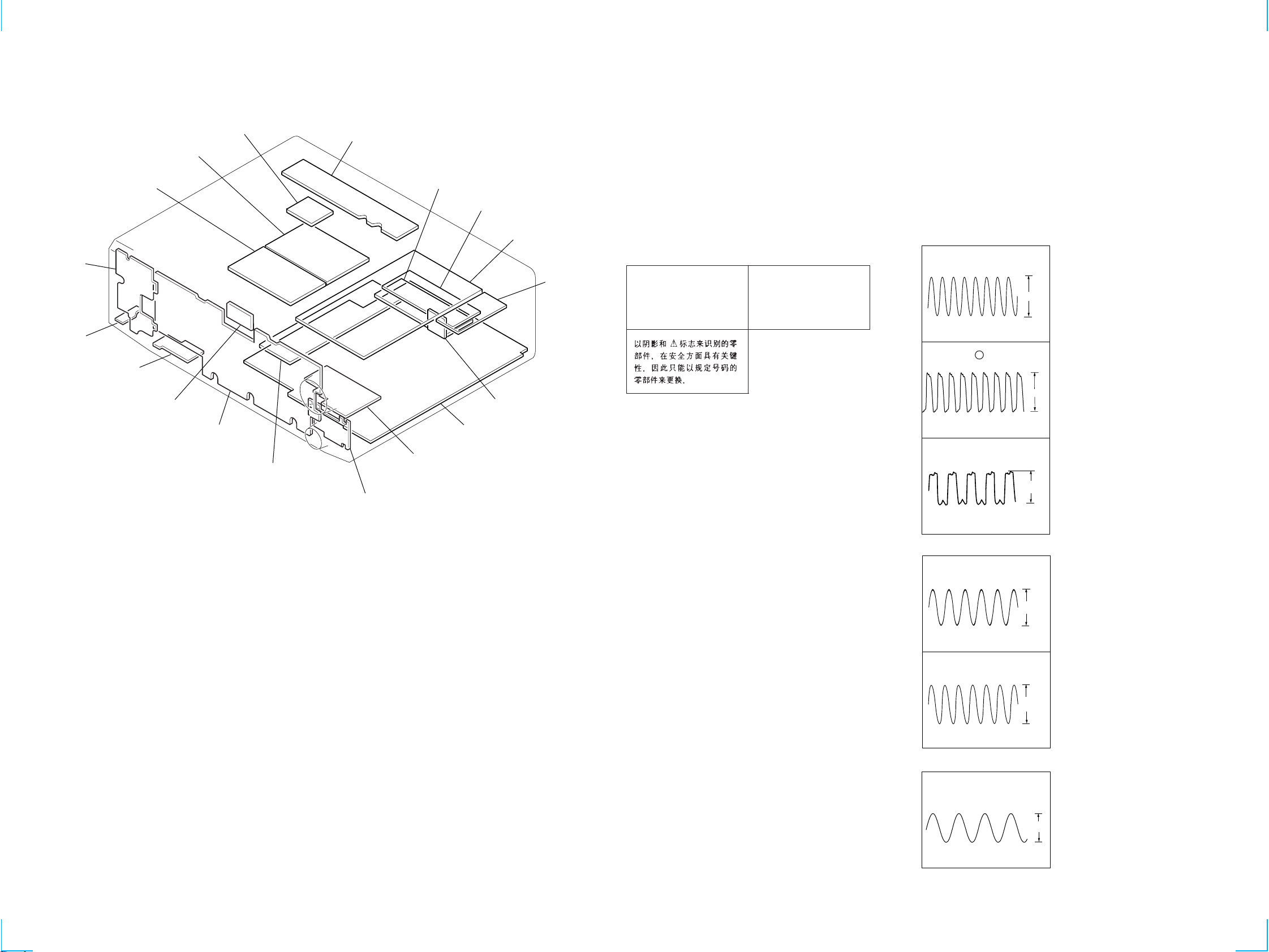
4-3. CIRCUIT BOARD LOCATION
AC board
DC board
SP-SW board
HP board
F-VIDEO board
LED board
4/8 board
DISPLAY board
REAR AMP board
SP SW board
ROTARY board
VIDEO board
S-VIDEO board
MAIN board
VOLUME board
DIGITAL board
TUNER
board
JOINT(Q) board
THIS NOTE IS COMMON FOR PRINTED WIRING
BOARDS AND SCHEMATIC DIAGRAMS.
(In addition to this necessary note is printed in each
block.)
For schematic diagrams.
Note:
• All capacitors are in µF unless otherwise noted. pF: µµF
50 WV or less are not indicated except for electrolytics
and tantalums.
• All resistors are in Ω and 1/
specified.
• % : indicates tolerance.
• 2 : nonflammable resistor.
• 1 : fusible resistor.
• C : panel designation.
Note:
The components identified by
mark ! or dotted line with mark
! are critical for safety.
Replace only with part number
specified.
• U : B+ Line.
• V : B– Line.
• H : adjustment for repair.
• Voltages and waveforms are dc with respect to ground
under no-signal (detuned) conditions.
No mark : FM
• V oltages are taken with a VOM (Input impedance 10 MΩ).
Voltage variations may be noted due to normal production
tolerances.
• Waveforms are taken with a oscilloscope.
• Circled numbers refer to waveforms.
• Signal path.
F : FM
J : CD
c : DIGITAL
I : PHONO
• Abbreviation
CND :Canadian model
AUS :Australian model
MY :Malaysia model
SP :Singapore model
CH :Chinese model
W or less unless otherwise
4
Note:
Les composants identifiés par
une marque ! sont critiques
pour la sécurité.
Ne les remplacer que par une
pièce portant le numéro spécifié.
For printed wiring boards.
Note:
• X : parts extracted from the component side.
• ® : Through hole.
• b : Pattern from the side which enables seeing.
• Wavef orm
DIGITAL Board
1 IC1201 (™ (XO)
4.0Vp-p
4MHz
2 IC1401 (CLKO)
100
3.5Vp-p
10MHz
3 IC1404 25
5.5Vp-p
12.288MHz
DISPLAY Board
4 IC102 *™ (XO)
3.6Vp-p
16.0MHz
TUNER Board
— 11 — — 12 —
5 IC106 !§ (X OUT)
3.8Vp-p
7.28MHz
6 IC1 !£ (X 1)
2.7Vp-p
4.33MHz
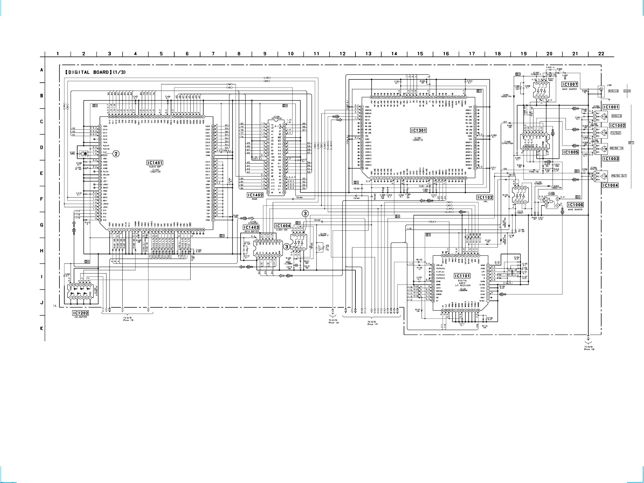
4-4. SCHEMATIC DIAGRAM DIGITAL SECTION(1/3) • See page 19 for Printed Wirig Board. • See page 12 for Waveforms. • See page 49 for IC Pin Functions. • See page 58 for IC Block Diagrams.
DIGITAL DOLBY,DTS DECODER
R1259
10k
STR-DB830/DB930/V929X
SIGNAL CHANGE
DATA SELECTOR
— 13 — — 14 —
STR-DB830/DB930/V929X
Ver 1.1 2002. 02
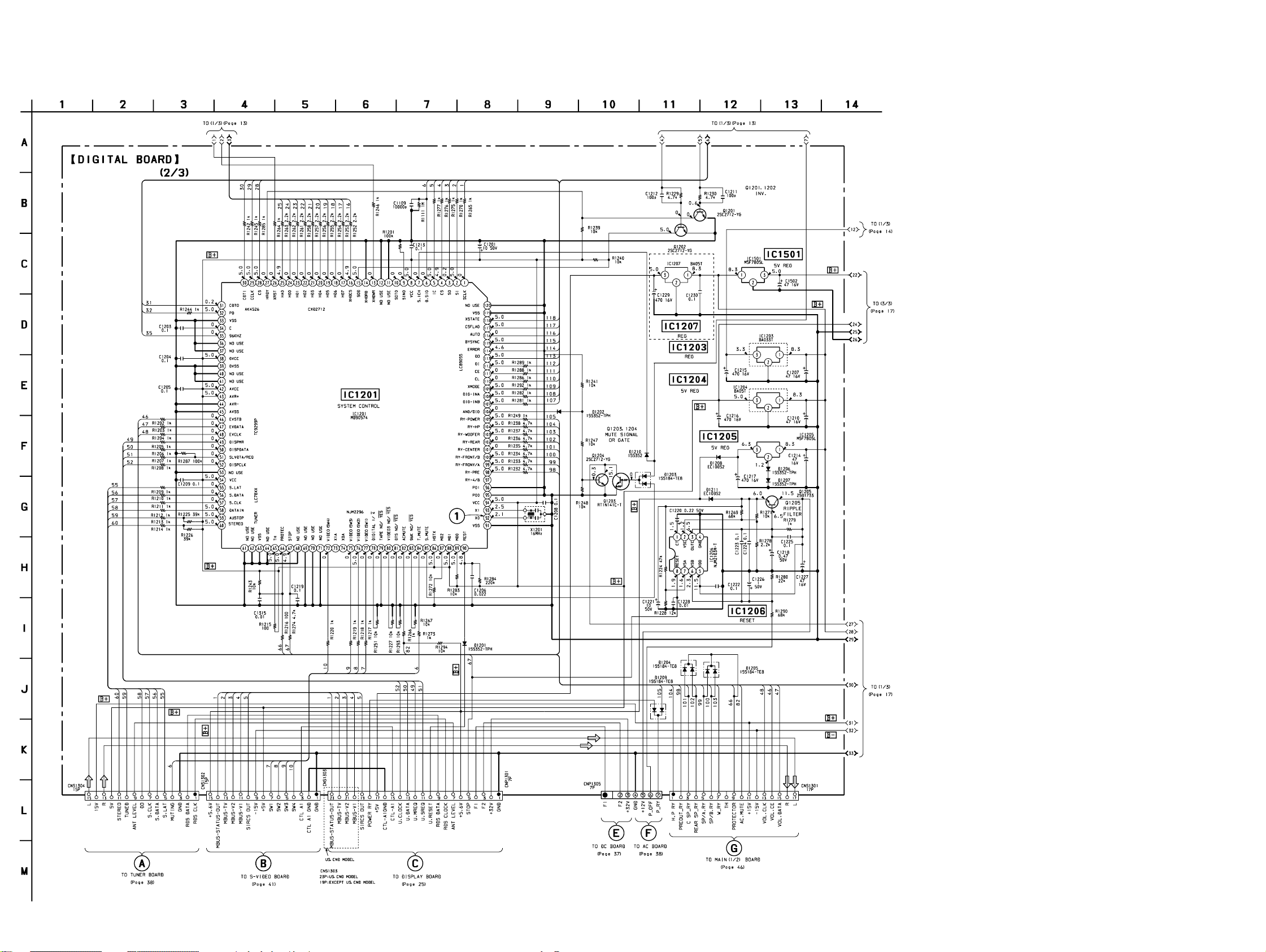
4-5. SCHEMATIC DIAGRAM DIGITAL SECTION(2/3) • See page 19 for printed wirig board. • See page 12 for Waveforms. • See page 51 for IC Pin Functions. • See page 58 for IC Block Diagrams.
DIGITAL PWB
CXD9511Q
FROM SUFFIX-12
+3.3V
— 15 — — 16 —
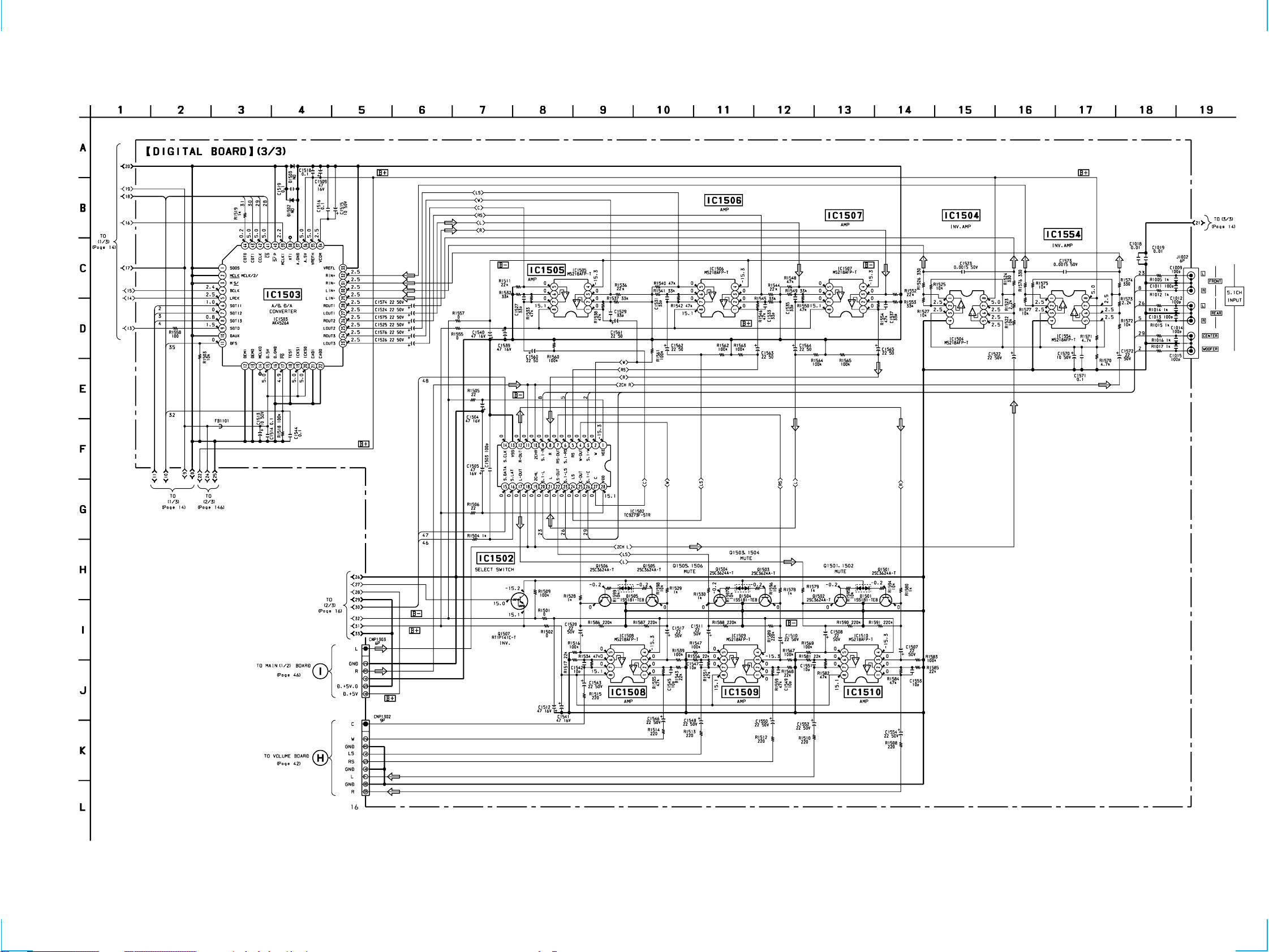
4-6. SCHEMATIC DIAGRAM DIGITAL SECTION(3/3) • See page 19 for printed wirig board. • See page 54 for IC Pin Functions. • See page 58 for IC Block Diagrams.
STR-DB830/DB930/V929X
— 17 — — 18 —
STR-DB830/DB930/V929X
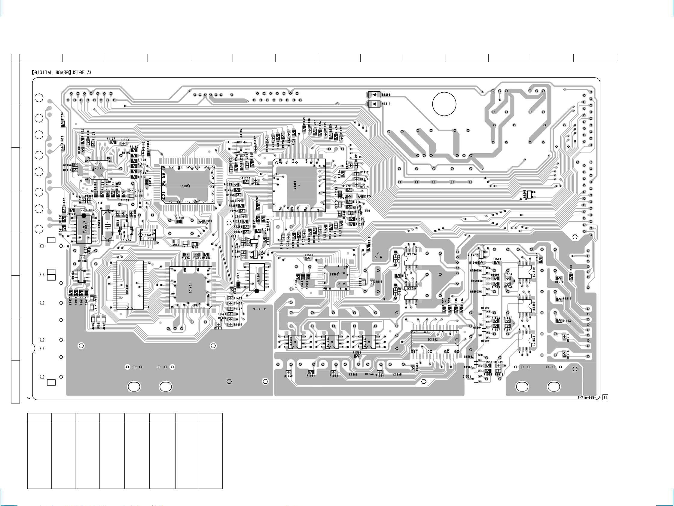
4-7. PRINTED WIRING BOARD DIGITAL SECTION(1/2) • See page 11 for circuit board location.
A
B
C
D
12
34567891011121314
E
F
G
H
• Semiconductor Location
Ref. No. Location Ref. No. Location
D1001 E-2
D1101 C-3
D1102 C-6
D1208 A-9
D1209 D-12
D1211 A-9
D1501 F-11
D1504 G-11
D1505 H-11
IC1005 D-2
IC1007 E-2
IC1101 C-2
IC1102 C-6
IC1201 C-7
IC1202 F-6
IC1301 C-4
IC1401 F-5
IC1402 F-3
IC1403 E-3
IC1404 D-3
IC1502 G-10
Ref. No. Location
IC1503 F-8
IC1504 F-10
IC1505 G-7
IC1506 G-8
IC1507 G-9
IC1508 G-12
IC1509 F-12
IC1510 E-12
IC1554 E-10
Q1201 E-6
— 19 — — 20 —
Ref. No. Location
Q1202 E-6
Q1501 E-11
Q1502 F-11
Q1503 F-11
Q1504 G-11
Q1505 G-11
Q1506 H-11
Q1507 E-11
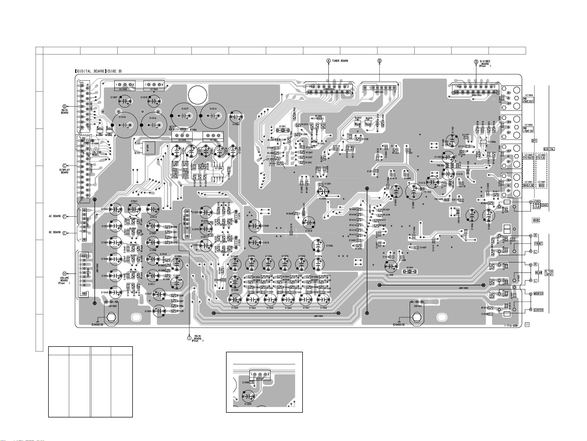
4-8. PRINTED WIRING BOARD DIGITAL SECTION(2/2) • See page 11 for circuit board location.
STR-DB830/DB930/V929X
Ver 1.1 2002. 02
C
D
A
B
12
(Page 44)
(Page 24)
345678910111213
VOLUME BOARD
39
US,CND,
EXCEPT
AUS
US,CND,
MODEL
AUS
MODEL
DB930,V929
MODEL
DB830
MODEL
(Page 36) (Page 40)
(Page 35)
E
(Page 36)
F
40
G
H
• Semiconductor Location
Ref. No. Location Ref. No. Location
D1002 C-12
D1201 C-7
D1202 B-8
D1203 B-9
D1204 C-2
D1205 C-2
D1206 C-4
D1207 C-4
D1210 B-10
IC1001 D-13
IC1002 C-13
IC1003 B-13
IC1004 B-13
IC1006 C-12
IC1203 A-3
IC1204 A-3
IC1205 C-4
IC1206 D-5
IC1501 C-5
Q1203 B-9
Q1204 C-8
Q1205 C-3
US,CND,
AUS
MODEL
EXCEPT
US,CND,
AUS
MODEL
43
DIGITAL PWB FROM SUFFIX-12
(Location B-6)
— 21 — — 22 —
STR-DB830/DB930/V929X
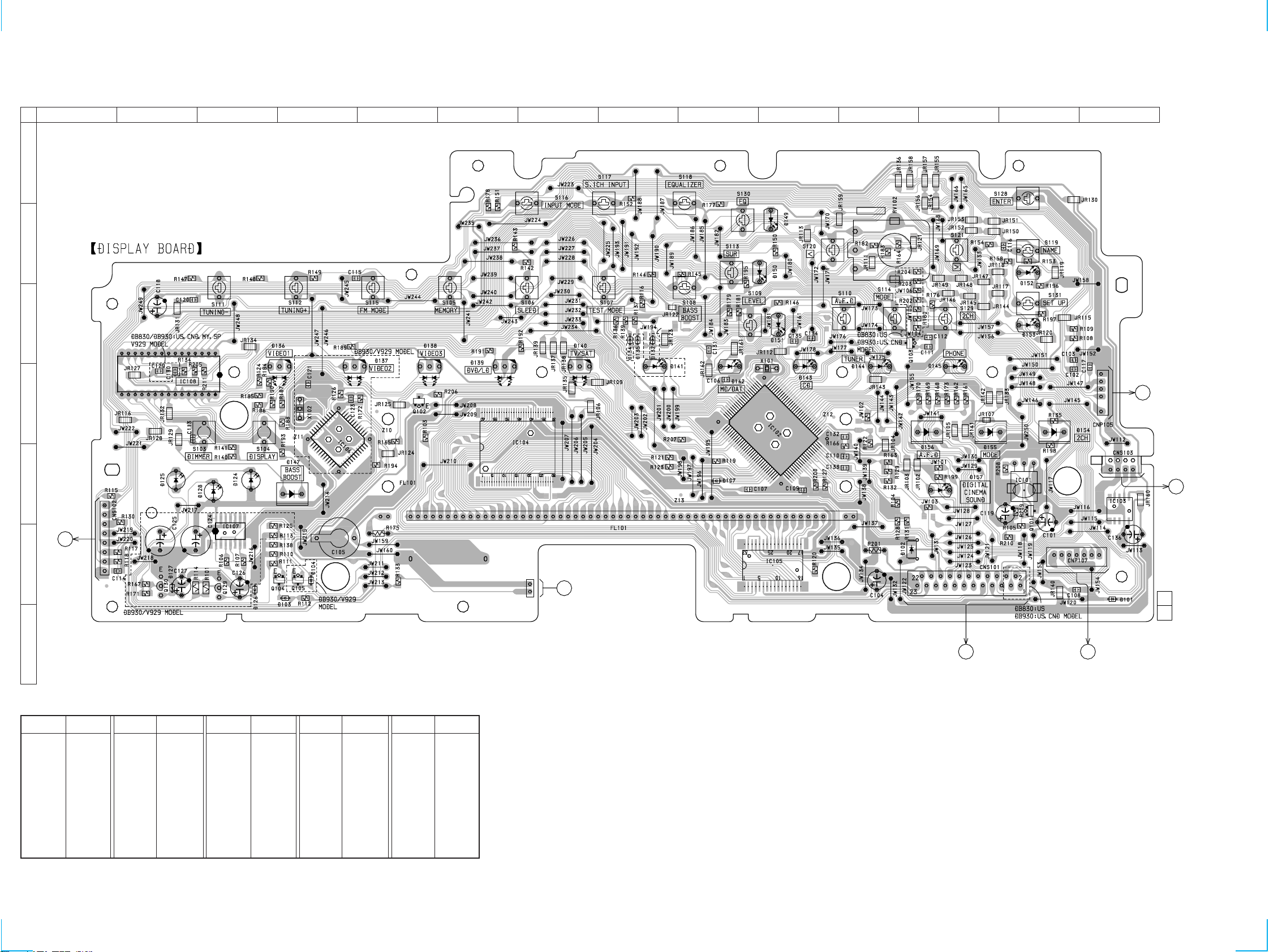
4-9. PRINTED WIRING BOARD DISPLAY SECTION • See page 11 for circuit board location.
C
D
A
B
12
34567891011121314
SPEAKERS
DB930:AEP,MY.SP,AUS
/V929
DB830
5
DB930/V929
80
J
ROTARY BOARD
100
1
50
1
(PAGE 27)
E
1
K
SP-SW
F
BOARD
(PAGE 28)
8
G
16
• Semiconductor Location
Ref. No. Location Ref. No. Location
D101 F-14
D102 F-11
D103 F-4
D104 F-4
D107 E-9
D124 E-3
D125 E-2
D126 F-4
D127 F-2
D128 E-3
D129 E-2
D132 C-8
D134 C-8
D135 C-8
D136 D-4
D137 D-4
D138 D-5
D139 D-6
D140 D-7
D141 D-8
D142 D-9
D143 D-10
Ref. No. Location
D144 D-11
D145 D-12
D147 E-4
D149 B-10
D150 B-10
D151 C-10
D152 B-13
D153 C-13
D154 D-13
D155 D-12
D156 D-12
Ref. No. Location Ref. No. Location
D157 E-12
Q101 E-13
Q102 D-5
IC101 E-13
IC102 D-10
IC103 E-14
IC104 E-7
IC105 F-10
Q103 C-11
Q104 F-4
Q105 F-4
Q129 F-3
Q130 F-2
IC106 E-4
IC107 F-3
IC108 D-2
CN120
1
2
LED BOARD
Z
(PAGE 28)
30
1
4
L
VOLUME
BOARD
(PAGE 40)
11
(11)
DIGITAL BOARD
C
(PAGE 21)
85
7
1
1-673-361-
VOLUME BOARD
X
(PAGE 40)
— 23 — — 24 —
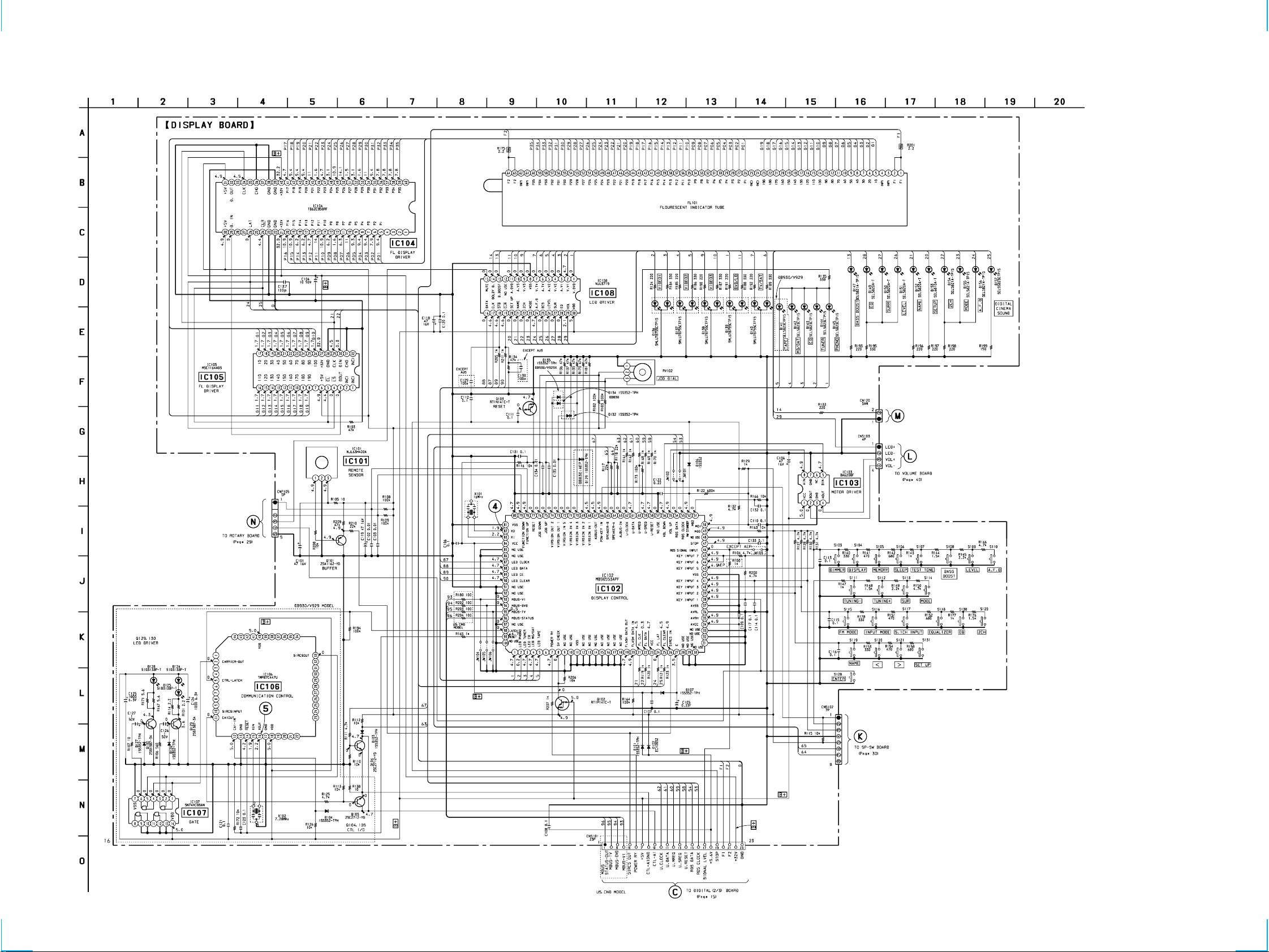
4-10. SCHEMATIC DIAGRAM DISPLAY SECTION • See page 12 for Waveforms. • See page 56 for IC Pin Functions. • See page 60 for IC Block Diagrams.
STR-DB830/DB930/V929X
SWITCH
TO LED BOARD
(PAGE 29)
— 25 — — 26 —
STR-DB830/DB930/V929X
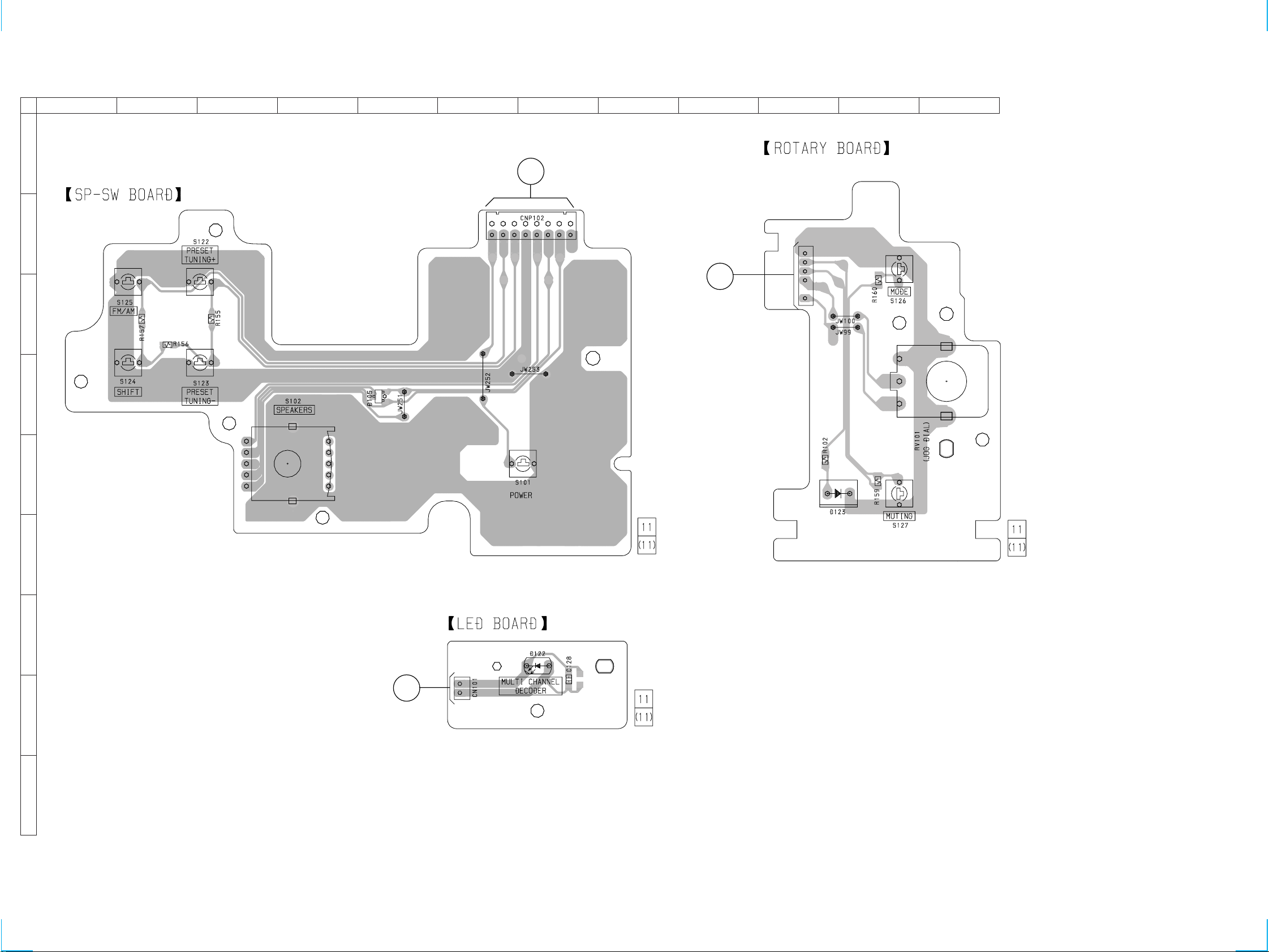
4-11. PRINTED WIRING BOARD SPEAKER SWITCH SECTION • See page 11 for circuit board location.
A
B
C
D
12
3456789101112
DISPLAY BOARD
K
8
(PAGE 23)
1
5
J
DISPLAY BOARD
(PAGE 24)
1
3
1
E
F
G
H
1-673-363-
1-673-364-
Z
DISPLAY BOARD
(PAGE 23)
1-673-366-
I
16
— 27 — — 28 —
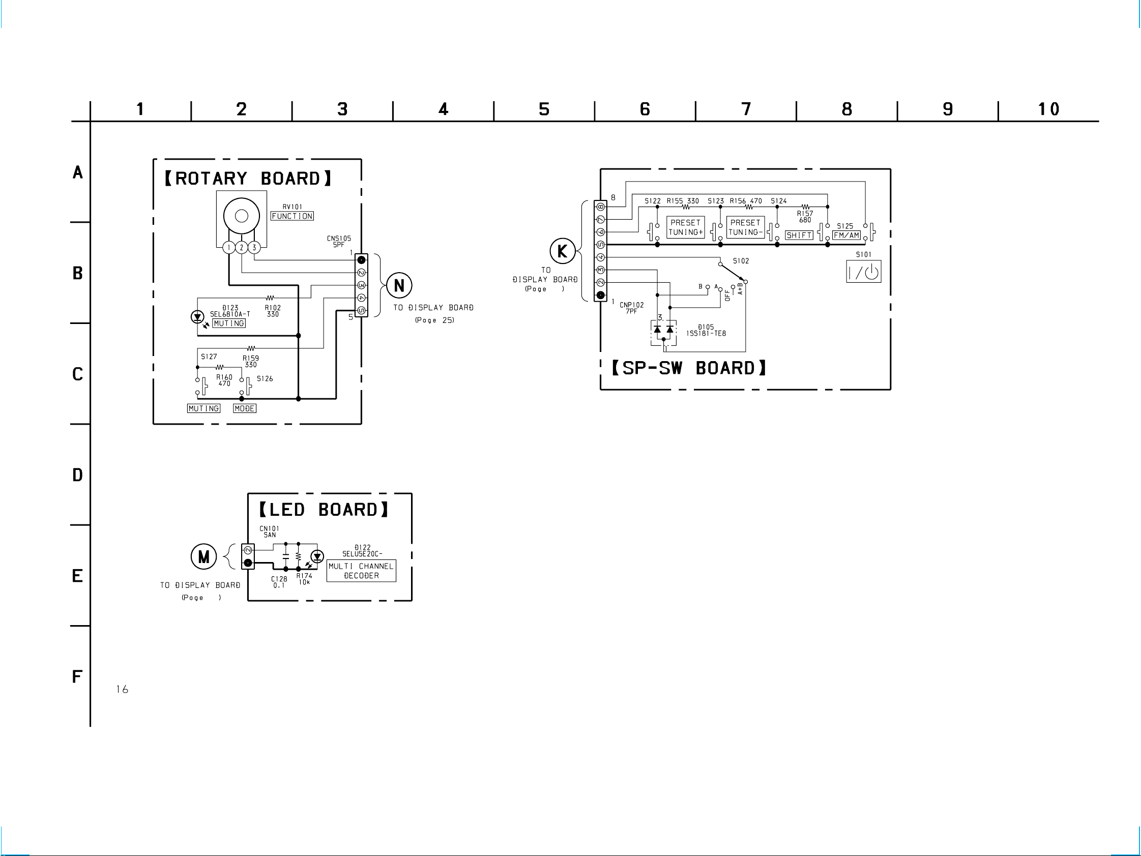
4-12. SCHEMATIC DIAGRAM SPEAKER SWITCH SECTION
STR-DB830/DB930/V929X
26
26
— 29 — — 30 —
STR-DB830/DB930/V929X
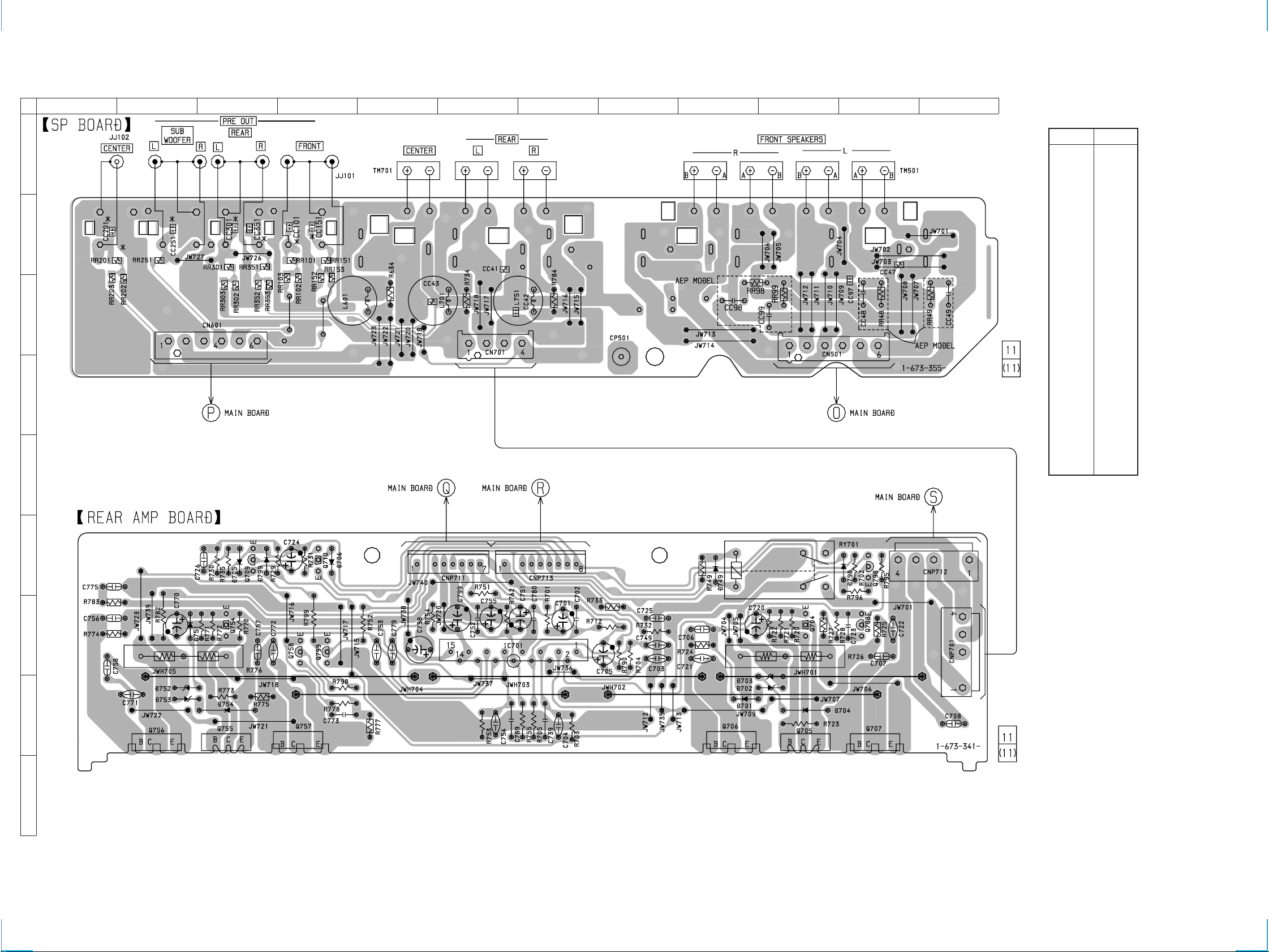
4-13. PRINTED WIRING BOARD REAR AMP SECTION • See page 11 for circuit board location.
A
B
C
D
E
12
AEP MODEL
3456789101112
(PAGE 43)(PAGE 43)
• Semiconductor
Location
Ref. No. Location
D701 H-9
D702 H-10
D703 H-10
D704 H-10
D705 F-3
D706 F-4
D749 F-9
D751 G-2
D752 H-2
D753 H-2
D754 H-3
D798 F-11
D799 F-3
IC701 G-6
Q704 G-10
Q705 H-10
Q706 H-9
Q707 H-11
Q708 G-11
Q709 F-3
Q710 F-4
Q754 G-3
Q755 H-3
Q756 H-2
Q757 H-4
Q758 G-4
Q798 F-11
Q799 G-4
F
G
H
(PAGE 44) (PAGE 43)
16
(PAGE 44)
I
— 31 — — 32 —
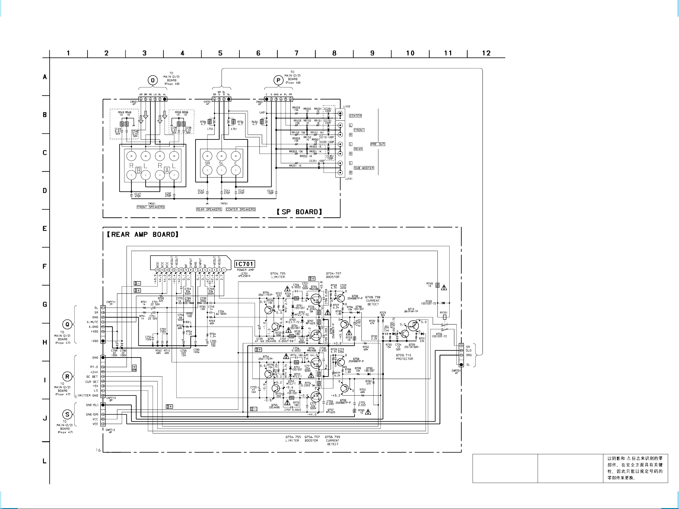
4-14. SCHEMATIC DIAGRAM REAR AMP SECTION • See page 58 for IC Block Diagrams.
STR-DB830/DB930/V929X
AEP MODEL
AEP MODEL
AEP MODEL
The components identified by
mark ! or dotted line with mark
! are critical for safety.
Replace only with part number
specified.
— 33 — — 34 —
Les composants identifiés par
une marque ! sont critiques
pour la sécurité.
Ne les remplacer que par une
pièce portant le numéro spécifié.
STR-DB830/DB930/V929X
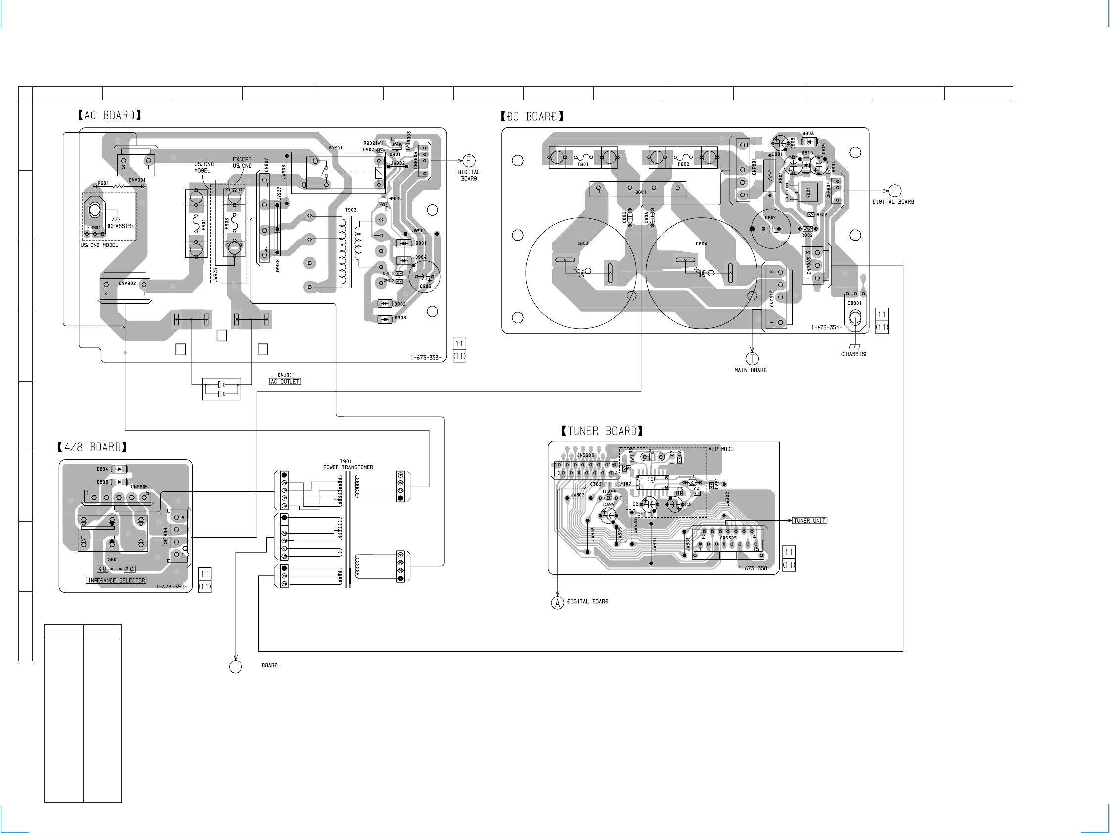
4-15. PRINTED WIRING BOARD POWER SECTION • See page 11 for circuit board location.
A
B
C
D
12
34567891011121314
4
1
(Page 21)
(Page 21)
(Page 44)
E
F
G
16
• Semiconductor
Location
H
Ref. No. Location
D801 B-9
D804 F-2
D805 F-2
D806 A-12
D810 B-12
D901 C-6
D902 C-6
D903 D-6
D904 C-6
D905 B-6
D907 A-5
U
(Page 22)
MAIN
(Page 44)
IC1 F-9
IC399 F-12
Q801 B-12
Q901 A-5
— 35 — — 36 —
 Loading...