

Page 1
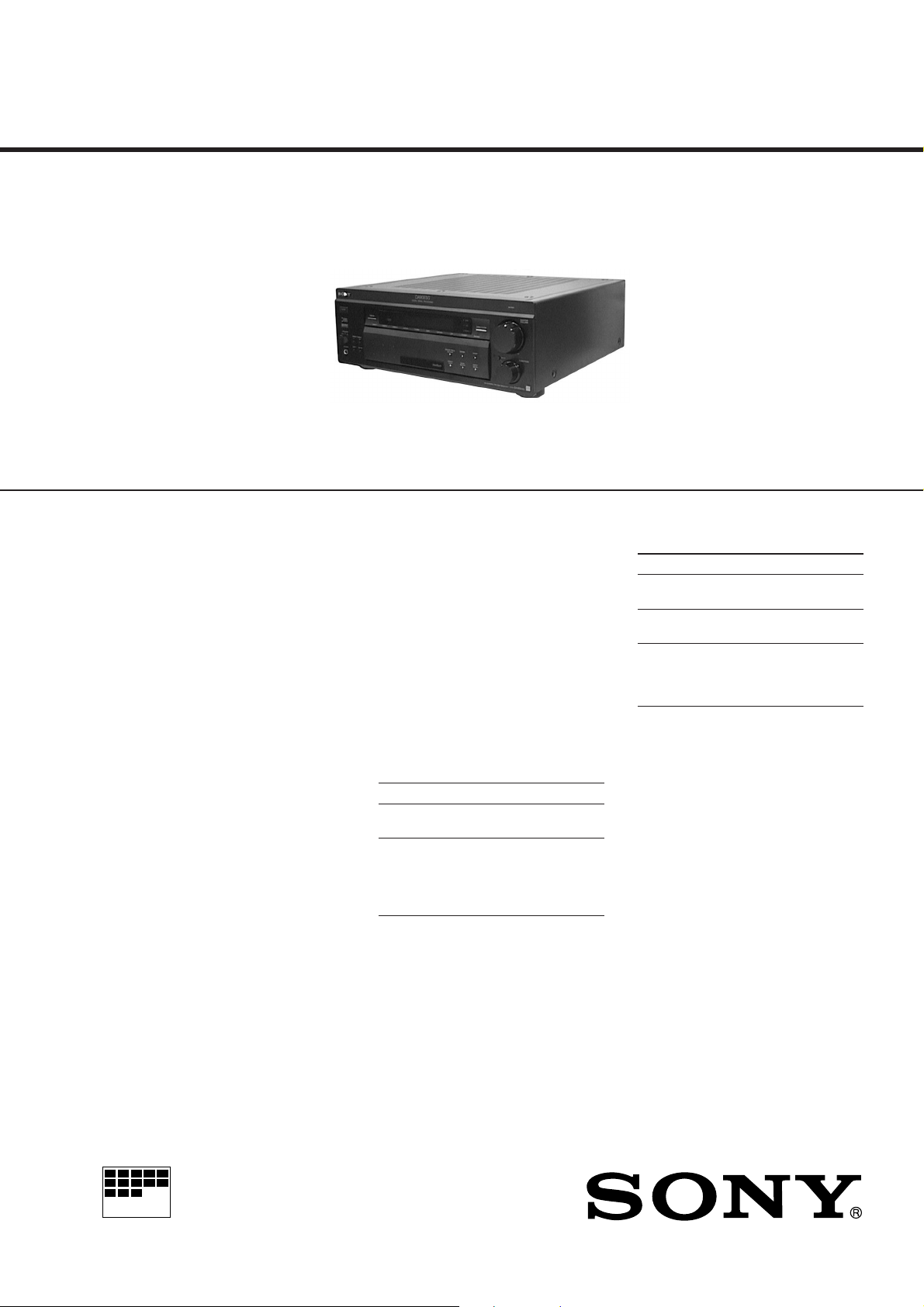
STR-DA90ESG
SERVICE MANUAL
Manufactured under license from Dolby
Laboratories Licensing Corporation.
“Dolby , ” the double-D symbol a, “AC-3” and
“Pro Logic” are trademarks of Dolby Laboratories Licensing Corporation.
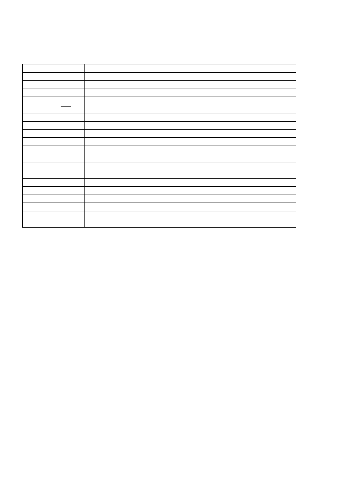
SPECIFICATIONS
Audio power specificaitons
POWER OUTPUT AND TOTAL
HARMONIC DISTORTION
With 8-ohm loads both channels
driven, from 20 - 20,000 Hz; rated 120
watts per channel minimum RMS
power, with no more than 0.05 % total
harmonic distortion from 250 miliwatts
to rated output (US model only).
Amplifier section
POWER OUTPUT
Stereo mode 8 ohms 20 Hz - 20 kHz,
THD 0.05 %,
120 W + 120 W
Surround mode (8 ohms at 1 kHz, THD
0.05 %)
Front: 120 W + 120 W
Center*: 120 W
Rear*: 120 W + 120 W
* No sound may be out-
put when using certain
sound sources and/or
sound mode settings.
Dynamic power 165 W + 165 W, 8 ohms
output (US, 280 W + 280 W, 4 ohms
Canadian model)
Harmonic Less than 0.05 %
distortion at (Direct Pass)
rated output
Frequency PHONO: RIAA
response equalization curve
±0.5 dB
CD, TAPE, DAT/MD,
LD, DVD, TV/DBS,
VIDEO: 10 Hz - 50
kHz dB
(Direct Pass)
Input (ANALOG)
Sensitivity Impedance S/N
PHONO 2.5 mV 50 75 dB*
kilohms (A, 2.5 mV)
CD, T APE,
DAT/MD,
VIDEO, 200 mV 50 82 dB*
LD/DVD, kilohms (A, 200mV)
TV/DBS
US Model
Canadian Model
Australian Model
Input (DIGITAL)
Sensitivity Impedance S/N
LD/DVD – 75 ohms 100 dB
AC-3 RF (A, 20 kHz LPF)
LD/DVD – 75 ohms 100 dB
COAXIAL (A, 20 kHz LPF)
LD/DVD,CD,
DAT/MD, – – 100 dB
TV/DBS, (A, 20 kHz LPF)
OPTICAL
* '78 IHF
+0.5
–2
Outputs REC OUT:
DAT/MD, TAPE
Voltage: 200 mV
Impedance: 1 kilohms
AUDIO OUT:
VIDEO 1, 2
Voltage: 200mV
Impedance: 1 kilohms
PRE OUT
Voltage: 2V
Impedance: 1 kilohms
PHONES: Accepts low
and high impedance
headphones
BASS BOOST +6 dB at 70 Hz
MICROFILM
– Continued on page 2 –
FM STEREO/FM-AM RECEIVER
Page 2

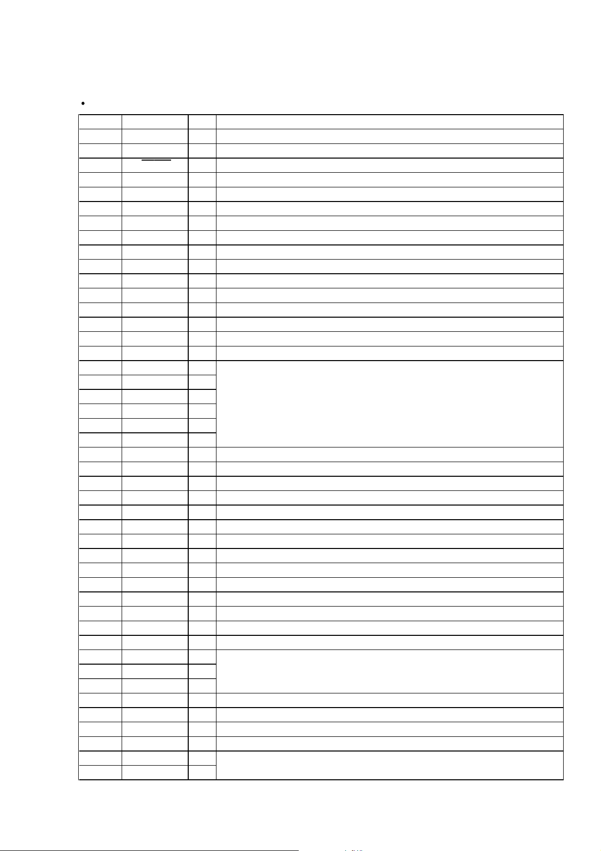
Digital Signal Processor section
Modulation High Density Linear
(A/D conversion) Converter
Demodulation High Density Linear
(D/A conversion) Converter (Advanced
Pulse D/A converter)
Sampling 48 kHz
frequency
Surround LFE MIX
MUTE, –20 ~ 0 dB, 0.5
dB step
D.RANGE COMP
OFF, 0.1 ~ 0.9, STD,
MAX
REAR level
–20 ~ +10 dB, 0.5 dB
step
CENTER level
–20 ~ +10 dB, 0.5 dB
step
SUB WOOFER level
–20 ~ +10 dB, 0.5 dB
step
WALL
17-step adjustable
SEAT
L/R 17-step adjustable
F/R 17-step adjustable
EFFECT
21-step adjustable
REVERB time
17-step adjustable
Equalizer Band
BASS/TREBLE
Turnover frequency
BASS: 99 Hz ~ 992 Hz
TREBLE: 1.0 kHz ~
8.6 kHz
Level
±10 dB, 0.5 dB step
FM tuner section
Tuning range 87.5 - 108.0 MHz
Antenna 75 ohms, unbalanced
terminals
Sensitivity Mono: 18.3 dBf, 4.5 µV
Stereo: 38.3 dBf, 45 µV
Usable sensitivity 11.2 dBf, 2 µV (IHF)
S/N Mono: 76 dB
Stereo : 70 dB
Harmonic Mono: 0.3 %
distortion at Stereo: 0.5 %
1 kHz
Separation 45 dB at 1 kHz
+0.5
Frequency 30 Hz - 15 kHz dB
–2
response
Selectivity 60 dB at 400 kHz
AM tuner section
Tuning range With 10 kHz interval*:
530 - 1710 kHz
US, Canadian model
With 9 kHz interval:
531 - 1710 kHz
US, Canadian model
531 - 1602kHz
Australian model
Antenna Loop antenna
Usable sensitivity 50 dB/m (at 1,000 kHz or
999 kHz)
S/N 54 dB (at 50 mV/m)
Harmonic 0.5 % (50 mV/m,
distortion 400 kHz)
Selectivity At 9 kHz: 35 dB
At 10 kHz: 40 dB
* You can change the AM tuning interval be-
tween 9 kHz and 10 kHz. After tuning in any
AM station, turn off the receiver. While holding down the PRESET + button, press the
POWER switch. When you change the interval, all the preset stations will be erased. To
reset the interval, repeat the same procedure.
US, Canadian model
Video section
Inputs VIDEO:
1 Vp-p 75 ohms
S-VIDEO:
Y: 1 Vp-p 75 ohms
C: 0.286 Vp-p 75 ohms
Outputs VIDEO:
1 Vp-p 75 ohms
S-VIDEO:
Y: 1 Vp-p 75 ohms
C: 0.286 Vp-p 75 ohms
General
System Tuner section:
PLL quartz-locked
digital synthesizer system
Preamplifier section:
Low-noise NF type
equalizer
Power amplifier section:
Pure-complimentary
Parallel P.P.
Power Australian models:
requirements 240 V AC, 50 Hz
US, Canadian models:
120 V AC, 60 Hz
Power Australian models: 430 W
consumption US models: 385 W
Canada models: 550 VA
AC outlets Australian models:
1 switched, total 100 W
US, Canadian models:
2 switched, total 120 W
Dimensions 430 × 160 × 435 mm
(17 × 6
3
/8 × 171/4 inches)
Mass (Approx.) 16.0 kg (35 lb 4 oz)
Supplied • FM wire antenna (1)
accessories • AM loop antenna (1)
• Remote commander
(remote) (1)
(remote for US and
Canadian models:
RM-H501)
(Remote for Australian
model: RM-VR101)
• Size AA (R6) batteries
(2)
• IR repeater (1)
– 2 –
Design and specifications are subject to change
without notice.
Page 3
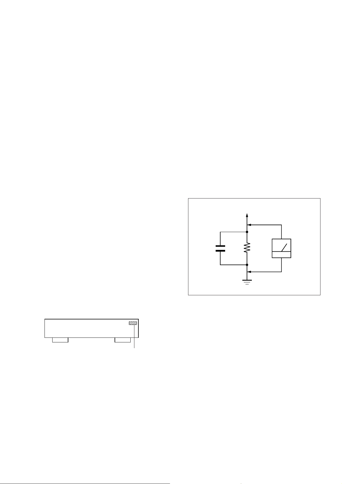
TABLE OF CONTENTS
1.5 k
Ω
0.15 µF
AC
voltmeter
(0.75 V)
To Exposed Metal
Parts on Set
Earth Ground
1. GENERAL
................................................................... 4
2. DISASSEMBLY.......................................................... 5
3. ELECTRICAL ADJUSTMENTS ......................... 7
4. DIAGRAMS
4-1. IC Pin Function Description ............................................ 9
4-2. Printed Wiring Boards – DISPLAY Section – ................ 27
4-3. Schematic Diagram – DISPLAY Section – .................... 31
4-4. Schematic Diagram – VIDEO Section – ......................... 36
4-5. Printed Wiring Boards – VIDEO Section –.................... 41
4-6. Schematic Diagram
– INPUT/TUNER/POWER Section –............................. 45
4-7. Printed Wiring Boards
– INPUT/TUNER/POWER Section –............................. 49
4-8. Schematic Diagram – DIGITAL Section –...................... 54
4-9. Printed Wiring Board – DIGITAL Section – .................. 59
4-10. Schematic Diagram – AMP/OUTPUT Section – ............ 63
4-11. Printed Wiring Boards – AMP/OUTPUT Section –....... 67
5. EXPLODED VIEWS ................................................ 75
6. ELECTRICAL PARTS LIST................................ 79
SAFETY CHECK-OUT
After correcting the original service problem, perform the following safety check before releasing the set to the customer:
Check the antenna terminals, metal trim, “metallized” knobs,
screws, and all other exposed metal parts for AC leakage.
Check leakage as described below.
LEAKAGE TEST
The AC leakage from any exposed metal part to earth ground and
from all exposed metal parts to any exposed metal part having a
return to chassis, must not exceed 0.5 mA (500 microampers.).
Leakage current can be measured by any one of three methods.
1. A commercial leakage tester , such as the Simpson 229 or RCA
WT -540A. Follo w the manufacturers’ instructions to use these
instruments.
2. A battery-operated AC milliammeter. The Data Precision 245
digital multimeter is suitable for this job.
3. Measuring the voltage drop across a resistor by means of a
VOM or battery-operated AC voltmeter. The “limit” indication is 0.75 V, so analog meters must have an accurate lowvoltage scale. The Simpson 250 and Sanwa SH-63T rd ar e examples of a passive VOM that is suitable. Nearly all battery
operated digital multimeters that have a 2 V A C range are suitable. (See Fig. A)
MODEL IDENTIFICATION
– BACK PANEL –
4-991-373-
US Model : 0
Canadian Model : 1
Australian Model : 2
Fig. A. Using an AC voltmeter to check AC leakage.
π
π
π
SAFETY-RELATED COMPONENT WARNING!!
COMPONENTS IDENTIFIED BY MARK ! OR DOTTED LINE
WITH MARK ! ON THE SCHEMATIC DIAGRAMS AND IN
THE PARTS LIST ARE CRITICAL TO SAFE OPERATION.
REPLACE THESE COMPONENTS WITH SONY PARTS WHOSE
PART NUMBERS APPEAR AS SHOWN IN THIS MANUAL
OR IN SUPPLEMENTS PUBLISHED BY SONY.
ATTENTION AU COMPOSANT AYANT RAPPORT
À LA SÉCURITÉ!
LES COMPOSANTS IDENTIFIÉS P AR UNE MARQUE ! SUR
LES DIAGRAMMES SCHÉMATIQUES ET LA LISTE DES
PIÈCES SONT CRITIQUES POUR LA SÉCURITÉ DE
FONCTIONNEMENT. NE REMPLACER CES COM- POSANTS
QUE P AR DES PIÈCES SONY DONT LES NUMÉR OS SONT
DONNÉS DANS CE MANUEL OU DANS LES SUPPLÉMENTS
PUBLIÉS PAR SONY.
– 3 –
Page 4
This section is extracted from
instruction manual.
SECTION 1
GENERAL
– 4 –
Page 5
SECTION 2
2
four screws
(BVTP 3
×
8)
1
connector
(CNV902)
1
connector
(CNE910)
1
connector
(CND802)
1
connector
(CNE807)
1
connector
(CND3503)
2
seven screws
(BVTP 3
×
8)
2
ten screws
(BVTP 3
×
8)
2
seven screws
(BVTP 3
×
8)
2
screw
(BVTP 3
×
8)
4
back panel section
3
two screws
(BVTP 3
×
6)
DISASSEMBLY
Note: Follow the disassembly procedure in the n umerical order given.
CASE
1
two screws
(M 3
1
three screws
(M 3
×
8)
×
8)
2
2
1
three screws
(M 3
×
8)
case
3
1
two screws
(M 3
×
8)
REAR PANEL SECTION
– 5 –
Page 6
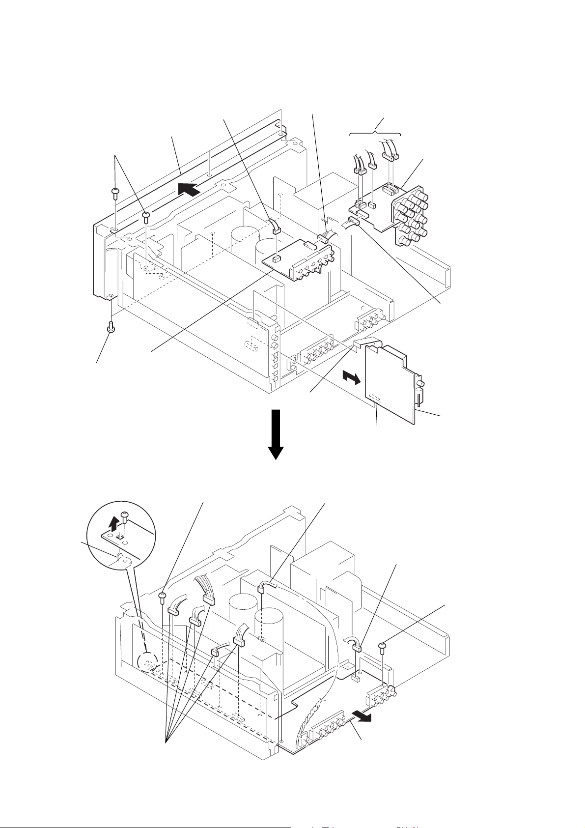
TUNER/AUDIO/SPTM BOARD, FRONT PANEL SECTION
1
7
four screws
(BVTP 3
7
three screws
(BVTP 3
×
8)
8
×
8)
3
AUDIO board
1
front panel section
connector
(CNE211)
connector
(CNS210)
1
five connectors
CND621, CNE601, 602,
(
CNV615, 616
)
2
SPTM board
1
connector
(CNS623)
INPUT BOARD
3
claw
2
five screws
(BVTP 3
4
flat wire
(CNS3503)
6
TUNER board
5
connector
(CNS201)
×
8)
1
connector
(CNV613)
1
connector
(CNE939)
2
screw
(BVTP 3
×
8)
1
five connectors
CNE601, 620, 622, 3501,
(
CNP202
4
INPUT board
)
– 6 –
Page 7
SECTION 3
ELECTRICAL ADJUSTMENTS
ON SCREEN SECTION
OSD ADJUSTMENT
Setting:
VIDEO output terminal
SET
S. VIDEO SG
VIDEO 1 S terminal
Procedure:
1. Connect the frequency counter to R813.
2. T urn the POWER switch ON, press VIDEO 1 and set the function to VIDEO 1. (The input signal set to OFF.)
3. Turn the POWER switch OFF, keep the BAND ,
depressed at the same time and then turn the POWER switch
ON.
4. Check that the screen shown only the color bars, and then adjust CT802 so that the reading becomes 3.5796 MHz ± 10 kHz.
5. Adjust CT801 so that the right edge of the color bars on the
screen comes within the frame.
Monitor TV
Vectroscope
buttons
INITIALIZATION OF THE MICROCOMPUTER
KEEP the DISPLAY , OPEN/CLOSE buttons depressed simultaneously and then turn the POWER switch ON.
Adjustment Location: VIDEO board (Component side)
CT802
IC814
RV801 CT801
R813
IC805
CT803
Frequency counter
(Picture of monitor screen)
RED
BLUE
DARK GRAY
Center
a=b
GRAY
ORANGE
WHITE
GREEN
BLACK
ab
6. The input signal set to ON.
BLUE
BLACK
(THROUGH)
GRAY
DARK GRAY
GREEN
(THROUGH)
WHITE
7. Turn the POWER switch OFF, keep the BAND , buttons
depressed at the same time and then turn the POWER switch
ON.
8. Adjust the picture frame as shown in (picture of monitor screen)
when using a color bar chart for adjustment with RV801.
– 7 –
Page 8
h
AMPLIFIRE SECTION
DC BIAS CURRENT Adjustment
(with no signal input)
Note:
1. DC BIAS CURRENT adjustments should be made 30 seconds after
the [POWER] switch is turned on (POWER ON).
2. After replacing the power transistors, DC BIAS CURRENT adjustments
should be perfomed.
Procedure:
1
2
3
Digital voltmeter
+
–
R665
1
2
3
AMP BOARD
R615
R665
R016
R715
R765
[AMP BOARD] (COMPONENT SIDE)
Connecting Adjustment Reading on
point part Digital voltmeter
FRONT Lch R615 RV601 20 mV
FRONT Rch R665 RV651 20 mV
CENTER R016 RV001 20 mV
REAR Lch R715 RV701 20 mV
REAR Rch R765 RV751 20 mV
C987
R618
FRONT Rch
REAR Rch
RV651
R668
R765
RV751
1
2
3
R768
R017
D973
C985
C986
RV001
C988
D971
D972
3
2
1
R715
R016
32
RV601
R615
R718
RV701
FRONT Lc
REAR Lch
3
2
1
1
CENTER
– 8 –
Page 9
SECTION 4
DIAGRAMS
4-1. IC PIN FUNCTION DESCRIPTION
DISPLAY BOARD IC105 MB90673PF-G-206-BND
(FLUORESCENT INDICATOR TUBE DRIVE CONTROLLER, KEY CONTROL)
Pin No. Pin Name I/O Function
1 MBUS (VZ) I
2 MBUS (MON) I
3 MBUS (STU) O
4 LED-V3 O
5 LED-V2 O
6 LED-V1 O
7 STANDBY O
8 DPC (SURR) O
9 DPC (EQ) O
10 DPC (INDEX) O
11 DVSS —
12 LED-CE O
13 LED-DAT/MD O
14 LED-TAPE O
15 LED-TV O
16 LED-LD O
17 LED-V3 O
18 LED-V2 O
19 LED-V1 O
20 RX (SIN) I
21 TX (SOUT) O
22 BUSY I
23 FL CLEAR O
24 FL DATA O
25 FL CLK O
26 LAT (OSD) O
27 SIRCS1 I
28 AVCC —
29 AVR+ I
30 AVR– I
31 GND —
32 AD KEY IN 1 I
33 AD KEY IN 2 I
34 DVSS —
35 AD KEY IN 3 I
36 AD KEY IN 4 I
37 AD KEY IN 5 I
38 AD VERSION I
39 VOL-UP I
40 VOL-DOWN I
41 MODE0 I
Not used (fixed at “L”)
Not used (fixed at “L”)
Not used (open)
LED drive signal output terminal “H”: LED on (for function VIDEO 3 indicator)
LED drive signal output terminal “H”: LED on (for function VIDEO 2 indicator)
LED drive signal output terminal “H”: LED on (for function VIDEO 1 indicator)
LED drive signal output terminal “H”: LED on Not used (open)
LED drive signal output terminal “H”: LED on (for SUR indicator)
LED drive signal output terminal “H”: LED on (for EQ indicator)
LED drive signal output terminal “H”: LED on (for INDEX indicator)
Ground terminal
LED drive signal output terminal “H”: LED on (for function CD indicator)
LED drive signal output terminal “H”: LED on (for function DAT/MD indicator)
LED drive signal output terminal “H”: LED on (for function TAPE indicator)
LED drive signal output terminal “H”: LED on (for function TV/DBS indicator)
LED drive signal output terminal “H”: LED on (for function LD/DVD indicator)
LED drive signal output terminal “H”: LED on (for function VIDEO 3 indicator)
LED drive signal output terminal “H”: LED on (for function VIDEO 2 indicator)
LED drive signal output terminal “H”: LED on (for function VIDEO 1 indicator)
Receive data input from the on screen display controller (IC809)
Transmit data output to the on screen display controller (IC809)
Busy signal input from the on screen display controller (IC809)
Display clear signal output to the fluorescent indicator tube driver (IC101, 102)
Serial data output to the fluorescent indicator tube driver (IC102)
Serial data transfer clock signal output to the fluorescent indicator tube driver (IC101, 102)
Serial data latch pulse signal output to the fluorescent indicator tube driver (IC101, 102)
Sircs signal input from the remote control receiver (IC104)
Power supply terminal (+5V)
Reference voltage input terminal (+5V)
Reference voltage input terminal (+0V)
Ground terminal
Key input terminal (A/D input)
S132 to 134 (INPUT MODE, DIRECT PASS, BASS BOOST keys)
Key input terminal (A/D input)
S116 to 119 (FM/AM, SHIFT, PRESET TUNING –/+ keys)
Ground terminal
Key input terminal (A/D input) S109 to 110 (EQUALIZER BAND, TUNING +/–, FM
MODE, MEMORY, DISPLAY keys)
Key input terminal (A/D input) S101 to 108 (EQUALIZER CH, DPC MODE,
cursor ←/↓/↑/→, SET UP, OPEN/CLOSE keys)
Key input terminal (A/D input)
S129 to 131 (MODE, SOUND FIELD ON/OFF, GENRE keys)
Setting terminal for the destination (A/D input)
Motor drive signal input for the master volume
Motor drive signal input for the master volume
Mode selection terminal (fixed at “H”)
– 9 –
Page 10
Pin No. Pin Name I/O Function
42 MODE1 I
43 MODE2 I
44 STANDBY I
45 STOP I
46 U-RESET I
47 U-SREQ O
48 U-MREQ I
49 U-DATA I/O
50 U-CLOCK I
51 HIFI/ES I
52 AUBUS-IN I
53 AUBUS-OUT O
54
55 FUNCTION-A I
56 OUT-OPEN O
57 OUT-CLOSE O
58 SW-OPEN I
59 SW-CLOSE I
60 — —
61 SWBAL I
62 RESET I
63 GND —
64 XO O
65 XI I
66 VCC —
67 LED-TUNER O
68 LED-PHONO O
69 LED MUTE O
70
71 LED D.PASS O
72 LED-INPUT O
73 LED VOL O
74 LED BASS.B O
75 SP-A I
76 SP-B I
77 PW-SW I
78 LED-TV O
79 LED-LD O
80 — I
FUNCTION-B
LED-LEARNING
Mode selection terminal (fixed at “H”)
Mode selection terminal (fixed at “L”)
Hardware standby signal input terminal (fixed at “H”)
Stop signal input terminal
System reset signal input from the master controller (IC3413) “L”: reset
Communication request signal output to the master controller (IC3413)
Communication request signal input from the master controller (IC3413)
Serial data in/out with the master controller (IC3413)
Serial data reading clock signal input from the master controller (IC3413)
Setting terminal for the destination (fixed at “H”)
Audio bus signal input terminal
Audio bus signal output terminal
I
Jog dial pulse input of the rotary encoder (RV101 FUNCTION)
Jog dial pulse input of the rotary encoder (RV101 FUNCTION)
Motor drive signal output to the door open/close motor drive (IC107)
Motor drive signal output to the door open/close motor drive (IC107)
Door open detect sensor (PH102) input terminal
Door close detect sensor (PH103) input terminal
Not used (open)
Balance volume on/off detect signal input terminal
Reset signal input terminal “L”: reset
Ground terminal
System clock signal output terminal (4MHz)
System clock signal input terminal (4MHz)
Power supply terminal (+5V)
LED drive signal output terminal “H”: LED on (for function TUNER indicator)
LED drive signal output terminal “H”: LED on (for function PHONO indicator)
LED drive signal output terminal “H”: LED on (for MUTING indicator)
O
LED drive signal output terminal “H”: LED on Not used (open)
LED drive signal output terminal “H”: LED on (for DIRECT PASS indicator)
LED drive signal output terminal “H”: LED on Not used (open)
LED drive signal output terminal “H”: LED on (for MASTER VOLUME illumination)
LED drive signal output terminal “H”: LED on (for BASS BOOST indicator)
Speaker select switch (S135) input terminal “H”: speaker A on
Speaker select switch (S135) input terminal “H”: speaker B on
Power switch (S137) input terminal
LED drive signal output terminal “H”: LED on (for function TV/DBS indicator)
LED drive signal output terminal “H”: LED on (for function LD/DVD indicator)
Not used (fixed at “L”)
– 10 –
Page 11
S VIDEO BOARD IC809 MB90T673PF-G-BND (ON SCREEN DISPLAY CONTROLLER)
Pin No. Pin Name I/O Function
1 AD14 I/O
2 AD15 I/O
3 A16 O
4 A17 O
5 A18 O
6 A19 O
7 PCE O
8 PCLK O
9 PDATA-OUT O
10 PDATA-IN I
11 GND —
12 ALE O
13 RDX O
14 WRLX O
15 WRHX O
16 CTR-S-MON O
17 CNT-S-V2 O
18 CTR-S-OUT O
19 CTR-S-V1 O
20 RX (SIN) I
21 TX (SOUT) O
22 RES O
23 — —
24 DATA (OSD) O
25 CLK (OSD) O
26 LAT (OSD) O
27 — —
28 AVCC —
29 AVR+ I
30 AVR– I
31 AVSS —
32 VOL A/D I
33 XP-RS I
34 GND —
35 P-TDAT I
36 P-OK I
37 M FULL I
38 BACK UP NG I
39 P-NG I
40 P-IR I
41 MODE0 I
42 MODE1 I
43 MODE2 I
44 HSTX I
45 STOP I
Two way data bus with the program ROM (IC820), S-RAM (IC822) and address data (for
address signal) output to the interface latch (IC818)
Address signal output to the program RAM (IC820)
Chip enable signal output to the program RAM (IC820) and S-RAM (IC821, 822)
Chip enable signal output to the RC controller (IC815)
Serial data transfer clock signal output to the RC controller (IC815)
Serial data output to the RC controller (IC815)
Serial data input from the RC controller (IC815)
Ground terminal
Address latch enable signal output to the interface latch (IC816, 818)
Read strobe signal output to the program RAM (IC820) and S-RAM (IC821, 822)
Write strobe signal output to the S-RAM (IC821) (for lower 8 bit)
Write strobe signal output to the S-RAM (IC822) (for higher 8 bit)
Not used (open)
Not used (open)
Not used (open)
Not used (open)
Receive data input from the FL drive controller (IC105)
Transmit data output to the FL drive controller (IC105)
Reset signal output to the RC controller (IC815) “L”: reset
Not used (open)
Serial data output to the MB90095PF-G (IC805)
Serial data transfer clock signal output to the MB90095PF-G (IC805)
Serial data latch pulse signal output to the MB90095PF-G (IC805)
Not used (open)
Power supply terminal (+5V)
Reference voltage input terminal (+5V)
Reference voltage input terminal (+0V)
Ground terminal
A/D conversion input terminal for the volume (fixed at “L”)
Data reception ready signal input from the RC controller (IC815)
Ground terminal
Infrared rays transmission data status signal input from the RC controller (IC815)
“H”: exist, “L”: nothing
Learning OK status signal input from the RC controller (IC815)
Memory full status signal input from the RC controller (IC815)
Backup NG status signal input from the RC controller (IC815)
Learning NG status signal input from the RC controller (IC815)
Learn IR signal input terminal “H”: no signal
Mode selection terminal (fixed at “H”)
Mode selection terminal (fixed at “L”)
Mode selection terminal (fixed at “L”)
Hardware standby signal input terminal (fixed at “H”)
Stop signal input terminal
– 11 –
Page 12
Pin No. Pin Name I/O Function
46 — —
47 — —
48 — —
49 AUBUS-IN I
50 V.SIGNAL I
51 SIRCS-IN I
52 NTSC/PAL I
53 AUBUS-OUT O
54
55 SEETH O
56 — —
57 — —
58 — —
59 — —
60 IR-OFF O
61 BUSY O
62 RESET I
63 GND —
64 XO O
65 XI I
66 VCC —
67 AD00 I/O
68 AD01 I/O
69 AD02 I/O
70 AD03 I/O
71 AD04 I/O
72 AD05 I/O
73 AD06 I/O
74 AD07 I/O
75 AD08 I/O
76 AD09 I/O
77 AD10 I/O
78 AD11 I/O
79 AD12 I/O
80 AD13 I/O
SCART (8)
Not used (open)
Not used (open)
Not used (open)
Audio bus signal input terminal
Video signal exist/without “H”: exist
Sircs signal input from the remote control receiver (IC104)
Detection signal input of the video system
Audio bus signal output terminal
O
Scart P8 control signal output terminal Not used (open)
See-through mode signal output terminal Not used (open)
Not used (open)
Not used (open)
Not used (open)
Not used (open)
IR on/off control signal output terminal
Busy signal output to the FL drive controller (IC105)
Reset signal input terminal “L”: reset
Ground terminal
System clock signal output terminal (4MHz)
System clock signal input terminal (4MHz)
Power supply terminal (+5V)
Two way data bus with the program ROM (IC820), S-RAM (IC821)
Two way data bus with the program ROM (IC820), S-RAM (IC821) and address data (for
address signal) output to the interface latch (IC816)
Two way data bus with the program ROM (IC820), S-RAM (IC821) and address data (for
address signal) output to the interface latch (IC818)
Two way data bus with the program ROM (IC820), S-RAM (IC822) and address data (for
address signal) output to the interface latch (IC818)
Two way data bus with the program ROM (IC820), S-RAM (IC822) and address data (for
address signal) output to the interface latch (IC816)
Two way data bus with the program ROM (IC820), S-RAM (IC822) and address data (for
address signal) output to the interface latch (IC818)
– 12 –
Page 13
S VIDEO BOARD IC815 LC86F5864A-5F53 (RC CONTROLLER)
Pin No. Pin Name I/O Function
1CEI
2 INT1 I
3 INT2 I Not used (fixed at “L”)
4IRI
5 STOP I Stop signal input terminal
6 DAT O
7NGO
8 BACK UP NG O
9 M FULL O
10 OK O
11 RS O
12 P37 O Not used (fixed at “L”)
13 P40 O Not used (fixed at “L”)
14 P41 O Not used (fixed at “L”)
15 P42 O Not used (fixed at “L”)
16 P43 O Not used (fixed at “L”)
17 P44 O Not used (fixed at “L”)
18 P45 O Not used (fixed at “L”)
19 P46 O Not used (fixed at “L”)
20 P47 O Not used (fixed at “L”)
21 SDA I/O Two-way data bus with the external EEPROM Not used (fixed at “L”)
22 SCL O Clock signal output to the external EEPROM Not used (fixed at “L”)
23 VSS2 —
24 VDD2 —
25 SDA I/O Two-way data bus with the external EEPROM Not used (fixed at “L”)
26 SCL O Clock signal output to the external EEPROM Not used (fixed at “L”)
27 TXD O Transmit data output terminal Not used (fixed at “L”)
28 RXD I Receive data input terminal Not used (fixed at “L”)
29 UCLK O Clock signal output terminal Not used (fixed at “L”)
30 P25 O Not used (fixed at “L”)
31 P26 O Not used (fixed at “L”)
32 P27 O Not used (fixed at “L”)
33 P00 O Not used (fixed at “L”)
34 P01 O Not used (fixed at “L”)
35 P02 O Not used (fixed at “L”)
36 P03 O Not used (fixed at “L”)
37 P04 O Not used (fixed at “L”)
38 P05 O Not used (fixed at “L”)
39 P06 O Not used (fixed at “L”)
40 P07 O Not used (fixed at “L”)
41 SO0 O
42 SI0 I
43 SCK0 I
44 SO1 O
45 SI1 I
Chip enable signal input from the on screen display controller (IC809)
Chip enable signal input terminal Not used (open)
Learn IR signal input terminal “H”: no signal
Infrared rays transmission data status signal output to the on screen display controller (IC809)
“H”: exist, “L”: noting
Learning NG status signal output to the on screen display controller (IC809)
Backup NG status signal output to the on screen display controller (IC809)
Memory full status signal output to the on screen display controller (IC809)
Learning OK status signal output to the on screen display controller (IC809)
Data reception ready signal output to the on screen display controller (IC809)
Ground terminal
Power supply terminal (+5V)
Serial data output to the on screen display controller (IC809)
Serial data input from the on screen display controller (IC809)
Serial data reading clock signal input from the on screen display controller (IC809)
Serial data output terminal Not used (open)
Serial data input terminal Not used (open)
– 13 –
Page 14
Pin No. Pin Name I/O Function
46 SCK1 I
47 BUZ O Not used (fixed at “L”)
48 PWM O Sircs signal output terminal
49 TEST1 O Test terminal Not used (open)
50 RES I Reset signal input from the on screen display controller (IC809) “L”: reset
51 XT1 I Sub system clock input terminal Not used (fixed at “L”)
52 XT2 O Sub system clock output terminal Not used (open)
53 VSS1 —
54 CF1 I Main system clock input terminal (6 MHz)
55 CF2 O Main system clock output terminal (6 MHz)
56 VDD1 —
57 AN0 I Not used (fixed at “L”)
58 AN1 I Not used (fixed at “L”)
59 AN2 I Not used (fixed at “L”)
60 AN3 I Not used (fixed at “L”)
61 AN4 I Not used (fixed at “L”)
62 AN5 I Not used (fixed at “L”)
63 AN6 I Not used (fixed at “L”)
64 AN7 I Not used (fixed at “L”)
Serial data reading clock signal input terminal Not used (open)
Ground terminal
Power supply terminal (+5V)
– 14 –
Page 15
DIGITAL BOARD IC3308 SN-PM4007A (DOLBY (AC-3) DEMODULATOR)
Pin No. Pin Name I/O Function
1 GND —
2 VDD —
3 RESET I
4 OSCON I
5 DATA I
6 MCK I
7 MLTB I
8 IDST O
9 IDCK O
10 IDO O
11 TM0 I
12 ECCK O
13 DEY O
14 DRY O
15 DRY O
16 TM1 I
17 A0 O
18 A1 O
19 A2 O
20 A3 O
21 A4 O
22 A5 O
23 TM2 I
24 TM3 I
25 XOUT O
26 XIN I
27 NEXT I
28 GND —
29 VDD —
30 A6 O
31 A7 O
32 GND —
33 VDD —
34 A12 O
35 A14 O
36 WE O
37 A13 O
38 A8 O
39 A9 O
40 GND —
41 A11 O
42 OE O
43 A10 O
44 D7 I/O
45 D6 I/O
Ground terminal
Power supply terminal (+5V)
Reset signal input from the master controller (IC3413) “L”: reset
Oscillation on/off control signal input terminal “H”: on (fixed at “H”)
Test terminal Not used (fixed at “L”)
Test terminal Not used (fixed at “L”)
Test terminal Not used (fixed at “L”)
Test terminal Not used (open)
Test terminal Not used (open)
Test terminal Not used (open)
Test terminal Not used (fixed at “L”)
Test terminal Not used (open)
Test terminal Not used (open)
Test terminal Not used (open)
Test terminal Not used (open)
Test terminal Not used (fixed at “L”)
Address signal output to the S-RAM (IC3309)
Test terminal Not used (fixed at “L”)
Test terminal Not used (fixed at “L”)
System clock output terminal Not used (open)
System clock input terminal Not used (fixed at “L”)
Test terminal Not used (fixed at “L”)
Ground terminal
Power supply terminal (+5V)
Address signal output to the S-RAM (IC3309)
Address signal output to the S-RAM (IC3309)
Ground terminal
Power supply terminal (+5V)
Address signal output to the S-RAM (IC3309)
Address signal output to the S-RAM (IC3309)
Write enable signal output to the S-RAM (IC3309) “L” active
Address signal output to the S-RAM (IC3309)
Ground terminal
Address signal output to the S-RAM (IC3309)
Output enable signal output to the S-RAM (IC3309) “L” active
Address signal output to the S-RAM (IC3309)
Two-way data bus with the S-RAM (IC3309)
– 15 –
Page 16
Pin No. Pin Name I/O Function
46 D5 I/O
47 D4 I/O
48 D3 I/O
49 D2 I/O
50 D1 I/O
51 D0 I/O
52 VDD —
53 GND —
54
55 VIN I
56 VOUT O
57 TI2 I
58 TI3 I
59 TLD8 I
60 TCK I
61 TRP O
62 TD0 O
63 PD0 O
64 TI4 I
65 PDD15 I
66 MUT0 O
67 TI5 I
68 VLDY O
69 DASYO O
70 DAOUT O
71 DAIN I
72 DASEL I
73 TI8 I
74 C2F1 O
75 C2F0 O
76 C1F1 O
77 C1F0 O
78 MUT1 I
79 VDD —
80 GND —
81 AVDD —
82 CPIN I
83 CMIN I
84 AGND —
85 TM4 I
86 VDD —
87 DIN I
TI1
Two-way data bus with the S-RAM (IC3309)
Power supply terminal (+5V)
Ground terminal
I
Test terminal Not used (fixed at “H”)
VCXO input terminal (18.432 MHz)
VCXO output terminal (18.432 MHz)
Test terminal Not used (fixed at “L”)
Test terminal Not used (fixed at “L”)
Test terminal Not used (fixed at “L”)
Test terminal Not used (fixed at “L”)
Test terminal Not used (open)
Test terminal Not used (open)
Internal phase comparator output terminal
Test terminal Not used (fixed at “L”)
PDO out control signal input terminal “L”: on
Mute control signal output terminal “H”: mute on
Test terminal Not used (fixed at “L”)
Test terminal Not used (open)
Test terminal Not used (open)
Digital out signal output terminal (serial data stream output)
Digital external input terminal Through out to DAOUT (pin &º) when DASEL (pin &™)is “H”
Not used (open)
Digital out selection terminal Fixed at “L”
Test terminal Not used (fixed at “L”)
C2 error correction state monitor output terminal Outputs if corrected properly
Not used (open)
C2 error correction state monitor output terminal Outputs number of errors at C2
Not used (open)
C1 error correction state monitor output terminal Outputs whether error is present at C1
Not used (open)
C1 error correction state monitor output terminal Outputs number of errors at C1
Not used (open)
Mute signal input terminal “H”: mute
Power supply terminal (+5V)
Ground terminal
Power supply terminal (+5V) (for analog system)
Comparator input (+) terminal
Comparator input (–) terminal
Ground terminal (for analog system)
Test terminal Not used (fixed at “L”)
Power supply terminal (+5V)
Test terminal Not used (fixed at “L”)
– 16 –
Page 17
Pin No. Pin Name I/O Function
88 DOUT O
89 DOUTB O
90 CSM O
91 GND —
92 WINGT O
93 SYST0 O
94 SYST1 O
95 ADST0 O
96 ADST1 O
97 TMS I
98 BUNR1 I
99 AGND —
100 AVDD —
Comparator output terminal
Comparator inverted output terminal
Clock (9.216 MHz) output terminal Not used (open)
Ground terminal
Test terminal Not used (open)
Test terminal Not used (open)
Test terminal Not used (open)
Test terminal Not used (open)
Test terminal Not used (open)
Test terminal Not used (fixed at “L”)
Test terminal Not used (fixed at “L”)
Ground terminal (for analog system)
Power supply terminal (+5V) (for analog system)
– 17 –
Page 18
DIGITAL BOARD IC3410 DSP56009FJ88F (DIGITAL SIGNAL PROCESSOR)
Pin No. Pin Name I/O Function
1 AGND —
2 MCS0 O
3 MCS3 O
4 MA14 O
5 MA13 O
6 AVCC —
7 MA12 O
8 AGND —
9 QVCC —
10 QGND —
11 MA11 O
12 MA10 O
13 MA9 O
14 MA8 O
15 AGND —
16 MA7 O
17 AVCC —
18 MA6 O
19 MA5 O
20 MA4 O
21 AGND —
22 MA3 O
23 MA2 O
24 MA1 O
25 MA0 O
26 SCK I
27 EXTAL I
28 QVCC —
29 QGND —
30 PINIT I
31 PGND —
32 PCAP I
33 PVCC —
34 SGND —
35 MISO I
36 RESET I
37 MODA I
38 MODB I
39 MODC I
40 SVCC —
41 MOSI O
42 SS I
43 HREQ I
44 SGND —
45 SDO2 O
Ground terminal (for address bus buffer)
Chip select signal output to the external RAM device Not used (open)
Chip select signal output to the external RAM device Not used (open)
Address signal output to the external RAM device Not used (open)
Address signal output to the external RAM device Not used (open)
Power supply terminal (+5V) (for address bus buffer)
Address signal output to the external RAM device Not used (open)
Ground terminal (for address bus buffer)
Power supply terminal (+5V) (for internal logic)
Ground terminal (for internal logic)
Address signal output to the external RAM device Not used (open)
Ground terminal (for address bus buffer)
Address signal output to the external RAM device Not used (open)
Power supply terminal (+5V) (for address bus buffer)
Address signal output to the external RAM device Not used (open)
Ground terminal (for address bus buffer)
Address signal output to the external RAM device Not used (open)
Serial data reading clock signal input from the master controller (IC3413)
Master clock signal input terminal (3MHz)
Power supply terminal (+5V) (for internal logic)
Ground terminal (for internal logic)
Initialize input for the PLL circuit (fixed at “L”)
Ground terminal (for PLL circuit)
Connected to the external capacitor for PLL circuit filter
Power supply terminal (+5V) (for PLL circuit)
Ground terminal (for serial port)
Communication data input from the master controller (IC3413)
Reset signal input from the master controller (IC3413) “L”: reset
Mode selection terminal (fixed at “H”)
Mode selection terminal (fixed at “L”)
Mode selection terminal (fixed at “H”)
Power supply terminal (+5V) (for serial port)
Communication data output to the master controller (IC3413)
SPI slave select signal input from the master controller (IC3413)
Host request signal input from the master controller (IC3413)
Ground terminal (for serial port)
Audio serial data output terminal Not used (open)
– 18 –
Page 19
Pin No. Pin Name I/O Function
46 SDO1 O
47 SDO0 O
48 SVCC —
49 SCKT O
50 WST O
51 SCKR I
52 QGND —
53 QVCC —
54
55 WSR I
56 SDI1 I
57 SDI0 I
58 DSO O
59 DSI I
60 DSCK I
61 DR I
62 MD7 I/O
63 MD6 I/O
64 MD5 I/O
65 MD4 I/O
66 DGND —
67 MD3 I/O
68 MD2 I/O
69 MD1 I/O
70 DVCC —
71 MD0 I/O
72 DGND —
73 GPIO3 I/O
74 GPIO2 I/O
75 GPIO1 I/O
76 GPIO0 I/O
77 MRD O
78 MWR O
79 MRAS O
80 MCAS O
SGND
Audio serial data output to the digital signal processor (IC3412)
Audio serial data output to the digital signal processor (IC3412)
Power supply terminal (+5V) (for serial port)
Audio serial data transfer clock signal output to the digital signal processor (IC3412)
Word transmission output to the digital signal processor (IC3412)
Bit clock signal (2.8224 MHz) input terminal
Ground terminal (for internal logic)
Power supply terminal (+5V) (for internal logic)
—
Ground terminal (for serial port)
L/R sampling clock signal (44.1 kHz) input terminal
Audio serial data input terminal
Audio serial data input terminal
Debug serial data output terminal Not used (open)
Debug serial data input terminal Not used (open)
Debug serial data reading clock signal input terminal Not used (open)
Debug request signal input terminal Not used (fixed at “H”)
Two-way data bus with the external RAM device Not used (open)
Ground terminal (for data bus buffer)
Two-way data bus with the external RAM device Not used (open)
Power supply terminal (+5V) (for data bus buffer)
Two-way data bus with the external RAM device Not used (open)
Ground terminal (for data bus buffer)
General digital signal processor in/out terminal Not used (open)
Write strobe signal output to the external RAM device Not used (open)
Read strobe signal output to the external RAM device Not used (open)
Row address strobe signal output to the external RAM device Not used (open)
Column address strobe signal output to the external RAM device Not used (open)
– 19 –
Page 20

DIGITAL BOARD IC3412 SSP424023FJ88 (DIGITAL SIGNAL PROCESSOR)
Pin No. Pin Name I/O Function
1 AGND —
2 MCS0 O
3 MA15 O
4 MA14 O
5 MA13 O
6 AVCC —
7 MA12 O
8 AGND —
9 QVCC —
10 QGND —
11 MA11 O
12 MA10 O
13 MA9 O
14 MA8 O
15 AGND —
16 MA7 O
17 AVCC —
18 MA6 O
19 MA5 O
20 MA4 O
21 AGND —
22 MA3 O
23 MA2 O
24 MA1 O
25 MA0 O
26 SCK I
27 EXTAL I
28 QVCC —
29 QGND —
30 PINIT I
31 PGND —
32 PCAP I
33 PVCC —
34 SGND —
35 MISO I
36 RESET I
37 MODA I
38 MODB I
39 MODC I
40 SVCC —
41 MOSI O
42 SS I
43 HREQ I
44 SGND —
45 SDO2 O
Ground terminal (for address bus buffer)
Chip select signal output to the external RAM device Not used (open)
Address signal output to the S-RAM (IC3411)
Power supply terminal (+5V) (for address bus buffer)
Address signal output to the S-RAM (IC3411)
Ground terminal (for address bus buffer)
Power supply terminal (+5V) (for internal logic)
Ground terminal (for internal logic)
Address signal output to the S-RAM (IC3411)
Ground terminal (for address bus buffer)
Address signal output to the S-RAM (IC3411)
Power supply terminal (+5V) (for address bus buffer)
Address signal output to the S-RAM (IC3411)
Ground terminal (for address bus buffer)
Address signal output to the S-RAM (IC3411)
Serial data reading clock signal input from the master controller (IC3413)
Master clock signal input terminal (3MHz)
Power supply terminal (+5V) (for internal logic)
Ground terminal (for internal logic)
Initialize input for the PLL circuit (fixed at “L”)
Ground terminal (for PLL circuit)
Connected to the external capacitor for PLL circuit filter
Power supply terminal (+5V) (for PLL circuit)
Ground terminal (for serial port)
Communication data input from the master controller (IC3413)
Reset signal input from the master controller (IC3413) “L”: reset
Mode selection terminal (fixed at “H”)
Mode selection terminal (fixed at “L”)
Mode selection terminal (fixed at “H”)
Power supply terminal (+5V) (for serial port)
Communication data output to the master controller (IC3413)
SPI slave select signal input from the master controller (IC3413)
Host request signal input from the master controller (IC3413)
Ground terminal (for serial port)
Audio serial data output terminal (for rear side speaker)
– 20 –
Page 21

Pin No. Pin Name I/O Function
46 SDO1 O
47 SDO0 O
48 SVCC —
49 SCKT O
50 WST O
51 SCKR I
52 QGND —
53 QVCC —
54
55 WSR I
56 SDI1 I
57 SDI0 I
58 DSO O
59 DSI I
60 DSCK I
61 DR I
62 MD7 I/O
63 MD6 I/O
64 MD5 I/O
65 MD4 I/O
66 DGND —
67 MD3 I/O
68 MD2 I/O
69 MD1 I/O
70 DVCC —
71 MD0 I/O
72 DGND —
73 GPIO3 I/O
74 GPIO2 I/O
75 GPIO1 I/O
76 GPIO0 I/O
77 MRD O
78 MWR O
79 CS1 O
80 MA16 O
SGND
Audio serial data output terminal (for center side speaker)
Audio serial data output terminal (for front side speaker)
Power supply terminal (+5V) (for serial port)
Bit clock signal (2.8224 MHz) output terminal
L/R sampling clock signal (44.1 kHz) output terminal
Audio serial data reading clock signal input from the digital signal processor (IC3410)
Ground terminal (for internal logic)
Power supply terminal (+5V) (for internal logic)
—
Ground terminal (for serial port)
Word transmission input from the digital signal processor (IC3410)
Audio serial data input from the digital signal processor (IC3410)
Audio serial data input from the digital signal processor (IC3410)
Debug serial data output terminal Not used (open)
Debug serial data input terminal Not used (open)
Debug serial data reading clock signal input terminal Not used (open)
Debug request signal input terminal Not used (fixed at “H”)
Two-way data bus with the S-RAM (IC3411)
Ground terminal (for data bus buffer)
Two-way data bus with the S-RAM (IC3411)
Power supply terminal (+5V) (for data bus buffer)
Two-way data bus with the S-RAM (IC3411)
Ground terminal (for data bus buffer)
General digital signal processor in/out terminal Not used (open)
General digital signal processor in/out with the master controller (IC3413)
Write strobe signal output to the S-RAM (IC3411)
Read strobe signal output to the S-RAM (IC3411)
Chip select signal output to the external RAM device Not used (open)
Address signal output to the S-RAM (IC3411)
– 21 –
Page 22

• DIGITAL BOARD IC3413 MB90641APF-G-104-BND (MASTER CONTROLLER)
Pin No. Pin Name I/O Function
1 RFERR I RF demodulater error signal input terminal “H”: error
2 RFRESET O RF demodulater reset signal output terminal “L”: active
3 STOP I System stop signal input terminal “L”: stop
4 RDATA I Data signal input from the digital audio interface receiver (IC3311)
5 WDATA O Data signal output to the digital audio interface receiver (IC3311)
6 DIRLAT O Latch pulse signal output to the digital audio interface receiver (IC3311)
7 DIRCLK O Clock signal output to the digital audio interface receiver (IC3311)
8 DIRERR I Error signal input from the digital audio interface receiver (IC3311)
9 ANG/DIG O Analog/Digital data select signal output to the selector (IC3414)
10 A/DINT O Initialize signal output to the A/D convertor (IC3104)
11 Vss — Ground terminal
12 HREQ I Host request signal input from the digital signal processor (IC3410)
13 SS O SPI slave select signal output to the digital signal processor (IC3410)
14 MOSI O Communication data output to the digital signal processor (IC3410)
15 RESET O Reset signal output to the digital signal processor (IC3410)
16 MISO I Communication data input from the digital signal processor (IC3410)
17 CLOCK O Serial data reading clock signal output to the digital signal processor (IC3410)
18 HREQ I Host request signal input from the digital signal processor (IC3412)
19 SS O SPI slave select signal output to the digital signal processor (IC3412)
20 MOSI O Communication data output to the digital signal processor (IC3412)
21 RESET O Reset signal output to the digital signal processor (IC3412)
22 MISO I Communication data input from digital signal processor (IC3412)
23 VCC — Power supply terminal (+5 V)
24 CLOCK O Serial data reading clock signal output to the digital signal processor (IC3412)
25 D/AINT O Initialize signal output to the digital filter (IC3401~3403)
26 D/ALAT O Latch pulse signal output to the digital filter (IC3401~3403)
27 C — Connect capacitor
28 D/ACLK O Serial data reading clock signal output to the digital filter (IC3401~3403)
29 D/ADATA O Data signal output to the digital filter (IC3401~3403)
30 SRCINI O Initialize signal output Not used (open)
31 D/A8DAT O 8bit data signal output to the D/A convertor Not used (open)
32 D/A8CLK O 8bit serial data reading clock signal output to the D/A convertor Not used (open)
33 D/A8LAT O 8bit la tch pulse signal output to the D/A convertor Not used (open)
34, 35 VCC — Power supply terminal (+5 V)
36, 37 VSS — Ground terminal
38
39
40
41
42 VSS — Ground terminal
43 to 47 N.C. — Not used (open)
48 STOPIN I Power check signal input terminal “L”: error
49 MD0 I Mode set terminal (fixed at “H”)
50 MD1 I Mode set terminal (fixed at “H”)
51 MD2 I Mode set terminal (fixed at “L”)
LOW-FRQ-IED
GAIN-FRONT-8DB
GAIN-FRONT-4DB
GAIN-FRONT-2DB
I General digital signal input from digital signal processor (IC3412)
O Front out +8 dB signal output terminal “H”: active
O Front out +4 dB signal output terminal “H”: active
O Front out +2 dB signal output terminal “H”: active
– 22 –
Page 23

Pin No. Pin Name I/O Function
52 STANDBY I Stand by signal input terminal (Fixed at “H”)
53 N.C. — Not used (open)
54 DISPMR I Communication request signal input from the FL drive controller (IC105)
55 DISPDATA I Serial data signal input from the FL drive controller (IC105)
56 SLVDATA/REQ O Communication request signal output to the FL drive controller (IC105)
57 DISPCLK I Serial data reading clock signal input from the FL drive controller (IC105)
58 LAT O Latch pulse signal output to the audio selector (IC202, 291)
59 DATA O Data signal output to the audio selector (IC202, 291)
60 CLK O Serial data reading clock signal output to the audio selector (IC202, 291)
61 DATAIN I PLL data signal input from the tuner unit (FE201)
62 AUTSTOP I PLL auto stop signal input from the tuner unit (FE201)
63 STEREO I PLL stereo signal input from the tuner unit (FE201)
64, 65 N.C. — Not used (open)
66 HIFI/ES I Not used (Fixed at “L”)
67 PROTEC I Amp output protect signal input terminal “L”: protect
68 VIDEO-A O Video input select signal “A” output to video input selector (IC803, 804, 811)
69 VIDEO-B O Video input select signal “B” output to video input selector (IC803, 804, 811)
70 VIDEO-E O Video input select signal “E” output to video input selector (IC803, 804, 811)
71 VIDEO-INH O Video monitor protect signal output terminal Not used (open)
72 FUNMUTE O Input mute signal output terminal
73 TUNERMUTE O Tuner mute signal output to the tuner unit (FE201)
74 SURR-MUTE O Surround mute signal output terminal
75 ALLMUTE O All mute signal output terminal Not used (open)
76 RM-MUTE O Signal level –20 dB mute signal output terminal
77 RESET O System reset signal output to the FL drive controller (IC105)
78 RY-FRONT/A O Front speakers “A” ON/OFF relay control signal output terminal “H”: on
79 RY-FRONT/B O Front speakers “B” ON/OFF relay control signal output terminal “H”: on
80 RY-FRONT O Front speakers ON/OFF relay control signal output terminal Not used (open)
81 VSS — Ground terminal
82 XO O System clock signal output terminal (4 MHz)
83 XIN I System clock signal input terminal (4 MHz)
84 VCC — Power supply terminal (+5 V)
85 RY-PREAMP O Pre out ON/OFF relay control signal output terminal “H”: on
86 RY-CENTER O Center speaker ON/OFF relay control signal output terminal “H”: on
87 RY-REAR O Rear speakers ON/OFF relay control signal output terminal “H”: on
88 RY-HP O Headphone ON/OFF relay control signal output terminal “H”: on
89 RY-4/8 O Speaker impedance select relay control signal output terminal “H”: 4 Ω
90 RY-POWER O Power ON/OFF relay control signal output terminal “H”: on
91 to 93 N.C. — Not used (open)
94
RY-DIRECT-PASS
95 RY-HD O Rear, center direct-pass relay control signal output terminal Not used (open)
96, 97 N.C. — Not used (open)
98 DIG-IN2 O Digital input select signal “C” output to the optical in select switch (IC3313)
99 DIG-IN1 O Digital input select signal “B” output to the optical in select switch (IC3313)
100 DIG-IN0 O Digital input select signal “A” output to the optical in select switch (IC3313)
O Direct-pass relay control sinal output terminal “L”: pass
– 23 –
Page 24

• Circuit Boards Location
MOTOR TM
board
SENSOR
board
HP board
SP SW board
PTB board
AMP board
PTA board
AC board
SP TM board
MEMORY board
S VIDEO board
CBV board
VIDEO board
TUNER board
INPUT board
AUDIO board
F. VIDEO board
CONNECTOR
board
DISPLAY board
BAL (B)
board
DIGITAL board
VOL board
BAL (A) board
– 24 –
Page 25

• Waveforms
– DISPLAY SECTION –
1 IC105 ^¢ 4 MHz
5 IC3402, 3403 0 48.5 MHz
9 IC3108 4
IC3425 1, 3 3.1 MHz
– DIGITAL SECTION –
2 IC3401 0 49 MHz
3 IC3401-3403 #•
IC3410 %¡
IC3414 7
IC3417 6 3.1 MHz
3.9 Vp-p
0.6 Vp-p
6 IC3407 1 6.1 MHz
7 IC3409 7
IC3410 %∞
IC3412 %º 48.1 kHz
0.6 Vp-p
4.9 Vp-p
5.1 Vp-p
0 IC3107 4 12.4 MHz
4.6 Vp-p
!¡ IC3104 !¶ 12.2 MHz
4 IC3401-3403 #ª
IC3414 4
IC3417 8 48.1 kHz
5.4 Vp-p
5.1 Vp-p
8 IC3104 !£
IC3108 8
IC3409 8 48.1 kHz
5.2 Vp-p
5 Vp-p
4.7 Vp-p
!™ IC3104 !¢ 3.1 MHz
5 Vp-p
– 25 –
Page 26

!£ IC3412 @¶ 3.1 MHz
!¶ IC3413 *™ 47 MHz
@¡ IC805 9 14.29
!¢ IC3410 @¶ 3.1 MHz
!∞ IC3311 @¡ 3.7 MHz
5 Vp-p
4.9 Vp-p
!• IC3308 %§ 18.52 MHz
– VIDEO SECTION –
!ª IC809 ^¢ 4 MHz
4.7 Vp-p
6 Vp-p
5.4 Vp-p
@™ IC810 0 520.8 kHz
0.8 Vp-p
@£ IC813 0 520.8 kHz
!§ IC3311 @™ 58.1 kHz
5.3 Vp-p
5.1 Vp-p
@º IC815 %¢ 6 MHz
3.6 Vp-p
4.2 Vp-p
0.8 Vp-p
@¢ IC814 #¡ 14.3 MHz
0.7 Vp-p
– 26 –
Page 27

• IC Block Diagrams
IC101 TD62C950RF (DISPLAY BOARD)
1
OUT1
20
OUT20
H V
P GND
L GND
CC
21
22
23
24
CL
NC
25
26
STB
27
NC
28
NC
S IN
29
V
DD
30
QD
ST
IC140 BA6208 (BAL (A) BOARD)
IC3311 CXD8521M (DIGITAL BOARD) IC3313 TC74HC151AF-TP1
13 12
TST2
14
SCLK/CL
15
XLAT/CE
D
CK
Q
ST
Q
D
Q
CK
D
OUT40
60
OUT21
41
40
CC
H V
39
P GND
38
L GND
37
NC
36
CHG
35
NC
34
CK
NC
33
32
S OUT
VDD
31
SWDT/DI
SRDT/DO
DQSY/LD
CKOUT
DATAOUT
ERROR
IC3401, 3402, 3403 CXD8505BQ (DIGITAL BOARD)
FS128
LRCK
MICOM
16
INTERFACE
17
18
19
20
TIMING
BCK
21
22
23
MUTE
24
OUTPUT
MUTER
SUB-Q
DET
C BIT
DET
DATA
DEMODURATE
LOCK ERROR
DET
TEST
SECTION
INVO2
INVO1
50
INPUT
TST1
11
AVOCK
10
XMODE
9
CKSEL
8
GND
7
VCO
PLL
VIN
6
5
R
4
VDD
E/DOUT
3
DIN2
2
1
DIN1
O
O
O
S
S
S
512F
256F
128F
INVI
TIMING
CIRCUIT
D3
D2
D1
D0
Y
XY
OE
GND
INAF
(DIGITAL BOARD)
1
D3D2
2
3
D1
4
D0
5
Y
6
W
7
SC
8
DATAI
VSUB(D)R
DFVSSVSUB(D)L
S/P
CC
V
16
D4
15
D4
14
D5
D5
13
D6
D6
12
D7
D7
11
A
A
10
B
B
9
C
SYSM
ATT
SHIFT
LATCH
INIT
BCKI
LRCKI
3334353637383940414244 43454647484951
XSEL
32
31
20/16
SWITCH
SWITCH
1 2 3 4 5 6 7
NC
INPUT 1
NC
INPUT 2
MOTOR
DRIVE
MOTOR
DRIVE
REG
Vcc
GND
IC3104 CXD8681M-TP (DIGITAL BOARD)
1
VREF+
VREF-
VCOML
AINL+
AINL-
ZCAL
VD
DGND
CAL
RST
SMODE 2
SMODE 1
LRCK
SCLK
VOLTAGE
REFERENCE
2
VOLTAGE
REFERENCE
3
4
DELTA-SIGMA
MODULATOR
5
DELTA-SIGMA
MODULATOR
6
7
DECIMATOR
8
9
CONTROLLER
10
DECIMATION
FILTER
CALIBRATION
SRAM
11
12
13
SERIAL OUTPUT
INTERFACE
14
28
27
26
25
24
23
22
21
20
19
18
17
16
15
OUTPUT 2
VREF+
VREFVCOMR
AINR+
AINRVA
AGND
BGND
TEST
SEL24
CMODE
MCLK
FSYNC
SDATA
8
OUTPUT1
9
NC
IC3108, 3407 TC74HC393AF-TP1
VIDEO IN
F.B CLAMP
SYNC OUT
VD OUT
NC
1
2
3
4
5
GND
6
EXC
(DIGITAL BOARD)
SYNC
SEP
V.SEP
COUNT
DOWN
LOCK
DET
32FH
“O” DETECT
MUTE
52
MUTEL
TEST1
53
54
TEST2
55
DFV
DD
2
56
DD
L
DV
57
SS
L
DV
58
VSUB(C)L
59
DD
2
V
DD
V
60
NC
14
L1(–)
L1(+)
VSS2
61
62
V
SS
63
64
1
2
34
2
SS
SS
V
V
L2(+)
L2(–)
Vcc
AFC
13
AFC CTL
12
VCO OUT
11
VCO
VCO IN
10
HD OUT
9
DET OUT
87
CIRCUIT
ATT
FIR1
IIR
FIR2
FIR3
3rd order
PLM PLM
NOISE SHAPER
5
DD
V
L.I.P
(X8)
6
7
2
DD
V
VSUB(A)L
MODE
AC, DC
DITHER
8
DD
XV
ATT
FIR1
IIR
FIR2
FIR3
L.I.P
3rd order
(X8)
NOISE SHAPER
CLOCK
GENERATOR
91011 12 13 14 15
XOUT
SSXVSS
XIN
DD2
V
XV
VSUB(A)R
DD
V
16 17 18 19
SS
V
R2(–)
R2(+)
30
SPLM
29
DFV
DD
1
28
DV
DD
R
27
DV
SS
R
26
VSUB(C)R
25
VDD2
24
V
DD
23
R1(–)
22
V
SS
21
R1(+)
20
SS
2
V
SS2
V
IC3409 TC5081AP (DIGITAL BOARD)
PHASE
COMPARATOR
1 2 3 4 5 6 7 8 9
AIN
AOUT
PDOUT
PHASE OUT
S
VDD
R
GND
N. C.
– 69 – – 70 –
Page 28

IC3516 LC7535M-TP (DIGITAL BOARD)
1
L 5dB IN
2
L CT1
3
L CT2
4
L 5dB OUT
5
L 1dB IN
6
L 1dB OUT
7
L VM
8
VEE
22
21
20
19
18
17
16
15
R 5dB IN
R CT1
R CT2
R 5dB OUT
R 1dB IN
R 1dB OUT
R VM
VCC
9
VDD
VSS
S
10
CONTROL
LEVEL SHIFT
+L
LATCH
+D
SHIFT RESISTER
D
IC802, 808 UBD4053BC (VIDEO BOARD)
VDDB. COM
16
1
B1
A. COM
A1
A0
A
B
C
15
14
2
3
B0
C1
13
4
C. COM
12
5
C0
10
11
6
INH
9
7
8
EE
SS
V
V
CE
14
DI
13
CLK
1211
– 71 –
Page 29

IC803, 804 SN761200N (S VIDEO BOARD)
IC811 SN761200N (VIDEO BOARD)
6dB
GND
IN5
GND
IN4
CTL E
IN3
1
2
3
4
5
6
7
MONITOR OUT
6dB
DECODER
IN1
16
15
CTL A
14
V OUT1
13
VCC
IN2
12
CTL B
11
V OUT2
10
CTL D
8
DECODER
IC805 MB90095PF-G-186-BND (VIDEO BOARD)
YIN
CIN
VIN
AVCC
FSCO
VBLK
VCC
EXS
HSYNC
VSYNC
1
2
3
4
5
6
7
8
XS
9
10
11
TO BLOCK
4FSC
CLOCK
OSC
NTSC/PAL
GENERATOR
SIGNAL
DISPLAY
MEMORY
CONTROL
ANALOG
SWITCH
VIDEO
SIGNAL
GENERATOR
OUTPUT
CONTROL
CGROM
SERIAL
INPUT
CONTROL
CTL C
9
IC810, 813 LA7217 (VIDEO BOARD)
GND
28
YOUT
27
COUT
26
25
VOUT
CS
24
23
S.DATA
22
S.CLK
TEST
21
VOC0
20
19
VOC1
VOC2
18
17
VOB
VIDEO IN
F.B CLAMP
SYNC OUT
VD OUT
GND
EXC
NC
1
SYNC
2
SEP
3
4
V.SEP
5
6
COUNT
DOWN
LOCK
DET
AFC
32FH
VCO
14
13
12
11
10
9
87
NC
Vcc
AFC CTL
VCO OUT
VCO IN
HD OUT
DET OUT
EXHSYN
EXVSYN
GND
12
13
14
H/V
SEPARATOR
VRAM
TO BLOCK
DOT CLOCK
OSC
XD
16
EXD
15
– 72 –
Page 30

IC814 MB3512PFQ (VIDEO BOARD)
W
VCC
36 35 33 32 31 30 29 28 27 26 2534
BGP
FSC
PS
XO
XI
XFO
XFI
PDF
CX
GND
C-B/
VIN
CC
A
VIN
A
CC
GND
(STAGE)
SVF
SVIN
SS-OUT
PLL-B
GND
GND
H
L
B/W DET
121110987654321
C-B/W
L
H
C AMP
Y AMP
24
23
22
21
20
19
18
17
16
15
14
13
GND
(STAGE)
CC
V
V-SW
B/W
A
37
38
-F
39
40
-F
41
42
43
44
45
46
47
48
CC
A
CC
PEDESTAL
CLAMP
SYNC
SEPARATER
SW3
(Y.SW)
AND
X'tal
PHASE
SHIFT
PHASE DET
L
H
L
PEDESTAL
BGP
CLAMP
FSC
PHASE
SHIFT
PHASE DET
PS
L
CC
V
H
X'tal
XI
XO
XFO
4fsc
AMP
4fsc
AMP
XFI
PDF
CK
IC816, 818 MC74HC373AN (MEMORY BOARD)
20
19
18 17 16 15 14 13 12
Q
D
C
OE
D
Q
C
OE
4
2D2Q1D
Q
OE
Q
OE
5 6 7 8 9
3Q
D
C
D
C
3D
1
OC
OUTPUT
CONTROL
Q
D
C
OE
Q
D
C
OE
2
3
1Q
(ENABLE)
5Q
5D6D6Q7Q7D8D8QVCC
D
C
OE
Q
C
OE
C
11
Q
D
10
4D4Q
GND
– 73 –
Page 31

IC202 LC7821 (INPUT BOARD)
IC291 LC7821 (AUDIO BOARD)
IC001, 601, 651 STK350-230
(INPUT BOARD)
L1
1
L2
2
3
L3
L4
4
5
L COM1
L5
6
L6
7
L COM2
8
9
L7
L8
10
L COM3
VEE
11
12
CE
13
DI
14
CL
15
BUFFER
CONTROL
LEVEL SHIFT
LATCH
SHIFT RESISTER
IC701 µPC2581V (INPUT BOARD)
BIAS CIRCUIT
PROTECTOR
4
COMP1
PRE
DRIVE
5
MF1
6
7
IN1
GND
REG DRIVE
1
2
MUTE
+ VOUT1
3
– VOUT1
IC901 NJM2103D (AC BOARD)
PRE
DRIVE
IN2
30
R1
29
R2
R3
28
R4
27
26
R COM1
25
R5
24
R6
R COM2
23
R7
22
21
R8
20
R COM3
19
VDD
RES
18
17
S
VSS
16
DRIVE
98
NF2
COMP2
1110
– VOUT2
12
+ VOUT2
13
VCC1
1514
VCC2
VEE
INPUT
-VEOUT
+VEOUT
GND
1
NF
2
3
4
5
6
7
V
SS
8
SUB
CC
V
9
D1 D2
TR1
TR2
R4
TR5
R5
R9
TR8
TR3 R1
TR4
TR7
R3
R8
R2
R6
TR6
D4 D3
R7
VSC
OUTC
GND
CR
1
2
+
–
3
4
VREF
Q
R S
+
–
8
RESET
+
–
VSA
7
6
VSB/SESIN
V+
5
+
–
– 74 –
Page 32

SECTION 5
EXPLODED VIEWS
NOTE:
• -XX and -X mean standardized parts, so they
may have some difference from the original
one.
• Color Indication of Appearance Parts
Example:
KNOB, BALANCE (WHITE) . . . (RED)
↑↑
Parts Color Cabinet's Color
(1) CASE SECTION
1
• Items marked “*” are not stocked since they
are seldom required for routine service. Some
delay should be anticipated when ordering these
items.
• The mechanical parts with no reference number in the exploded views are not supplied.
• Hardware (# mark) list and accessories and
packing materials are given in the last of the
electrical parts list.
2
3
The components identified by mark
! or dotted line with mark ! are
critical for safety.
Replace only with part number
specified.
Les composants identifiés par une
marque ! sont critiquens pour la
sécurité.
Ne les remplacer que par une pièce
portant le neméro spécifié.
1
1
#1
#1
#1
front panel section
#1
not supplied
Ref. No. Part No. Description Remark
1 3-704-366-01 SCREW (CASE) (M3X8)
* 2 4-982-090-01 CASE (414538E)
3 4-985-642-01 CUSHION
3
#1
4
5
#2
Ref. No. Part No. Description Remark
4 4-970-123-01 FOOT (F50180S)
5 4-970-124-01 CUSHION (F50180S)
– 75 –
Page 33

(2) FRONT PANEL SECTION
62
56
55
57
58
52
54
#3
not
supplied
53
#3
59
65
61
60
63
64
#3
66
#1
68
69
67
#3
93
#3
99
70
92
91
94
72
95
71
#3
87
73
86
96
85
M101
74
#1
84
#1
#4
75
77
97
not
supplied
#1
98
not
#1
supplied
83
supplied
with RV140
#1
#1
78
79
#1
not
supplied
76
#1
80
81
#1
82
51
Ref. No. Part No. Description Remark
51 4-991-378-01 PANEL, FRONT (US, Canadian)
51 4-991-378-71 PANEL, FRONT (Australian)
52 4-942-568-01 EMBLEM (NO.5), SONY
53 X-4948-618-1 LID (FRONT) ASSY
54 3-974-992-01 SLIDER (L), DOOR
55 4-991-596-01 SPRING, TENSION
56 4-991-406-01 FRAME (DOOR L)
57 X-4948-616-1 SHAFT (L) ASSY, DOOR DRIVING
58 4-991-393-01 LID (BASE)
* 59 1-666-331-11 CONNECTOR BOARD
60 4-991-394-01 LID (BACK)
61 4-957-383-01 KNOB (F14)
62 4-991-384-01 BUTTON (TUNER)
63 4-991-390-01 PANEL (WINDOW)
64 4-991-389-01 WINDOW (US, Canadian)
64 4-991-389-11 WINDOW (Australian)
65 A-4384-608-A BASE ASSY, GEAR
* 66 1-666-314-11 SENSOR BOARD
67 4-812-134-00 RIVET (DIA. 3.5), NYLON
68 3-325-697-01 WASHER
90
#3
55
88
89
Ref. No. Part No. Description Remark
* 76 A-4398-808-A DISPLAY BOARD, COMPLETE (US, Canadian)
* 76 A-4398-809-A DISPLAY BOARD, COMPLETE (Australian)
77 A-4384-609-A SHAFT (LINK) ASSY
78 4-991-383-01 BUTTON (SUB)
79 4-991-382-01 BUTTON (MAIN)
* 80 1-666-309-11 VOL BOARD
* 81 1-666-316-11 BAL (B) BOARD
* 82 1-666-315-11 BAL (A) BOARD
83 4-991-379-01 BASE, PANEL
84 4-991-385-01 BUTTON (MODE)
85 X-4948-600-1 KNOB (VOL) ASSY
86 X-4948-601-1 KNOB (FUNC) ASSY
87 X-4948-617-1 SHAFT (R) ASSY, DOOR DRIVING
88 3-974-989-01 SLIDER, DOOR (R)
89 4-991-407-01 FRAME (DOOR R)
90 4-991-387-01 INDICATOR (MUTE)
91 1-475-109-21 SWITCH (A) BLOCK, TOUCH
92 1-475-109-31 SWITCH (B) BLOCK, TOUCH
93 1-775-084-11 WIRE (FLAT TYPE) (9 CORE)
94 4-980-639-01 KNOB (R14)
69 3-975-016-01 GEAR (D)
70 3-377-720-01 WASHER, POLYETHYLENE
71 3-975-015-01 GEAR (C)
72 3-975-014-01 GEAR (B)
* 73 1-666-313-11 MOTOR TM BOARD
74 X-4948-598-1 BRACKET (MOTOR) ASSY
* 75 1-666-330-11 SP SW BOARD
95 4-979-936-01 BUTTON (P-T)
96 4-991-388-01 INDICATOR (FUNC)
97 4-991-391-01 FILTER
98 4-991-386-01 BUTTON (WINDOW)
99 4-995-595-01 SPACER (LID)
M101 A-4384-605-A MOTOR ASSY (DOOR OPEN/CLOSE)
– 76 –
Page 34

(3) BACK PANEL SECTION
152
T901
153
156
not
supplied
#5
#1
#5
#6
155
154
#1
169
#1
168
not
supplied
163
166
not
supplied
162
157
170
US,
Canadian
158
Australian
#1
#1
not
supplied
158
#1
161
Australian
CNS901
#1
#1
#1
160
#1
#1
#1
#1
151
Ref. No. Part No. Description Remark
* 151 1-666-305-11 F.VIDEO BOARD
* 152 1-666-304-11 HP BOARD
* 153 1-666-303-11 PTB BOARD
* 154 1-666-302-11 PTA BOARD
* 155 A-4398-793-A SP TM BOARD, COMPLETE
* 156 A-4398-794-A AC BOARD, COMPLETE (US, Canadian)
* 156 A-4398-795-A AC BOARD, COMPLETE (Australian)
* 157 3-703-244-00 BUSHING (2104), CORD (Australian)
157 4-916-783-01 BUSHING, CORD (US, Canadian)
! 158 1-559-479-11 CORD, POWER (US, Canadian)
164
chassis section
The components identified by
mark ! or dotted line with
mark ! are critical for safety.
Replace only with part number
specified.
Ref. No. Part No. Description Remark
* 161 4-991-373-21 PANEL (STR), BACK (Australian)
* 162 A-4398-801-A S VIDEO BOARD, COMPLETE
* 163 A-4398-799-A VIDEO BOARD, COMPLETE (US, Canadian)
* 163 A-4398-800-A VIDEO BOARD, COMPLETE (Australian)
* 164 A-4398-802-A AUDIO BOARD, COMPLETE
* 166 1-666-323-11 CBV BOARD
* 168 1-666-327-11 MEMORY BOARD
169 1-773-277-11 WIRE (FLAT TYPE) (29 CORE)
* 170 3-703-353-07 SUPPORT, PC BOARD
! CNS901 1-251-416-11 OUTLET, A.C. (Australian)
Les composants identifiés par une
marque ! sont critiques pour la
sécurité.
Ne les remplacer que par une pièce
portant le neméro spécifié.
! 158 1-690-608-11 CORD, POWER (Australian)
160 4-947-010-01 SCREW, FEEDER FIXED
* 161 4-991-373-01 PANEL (STR), BACK (US)
* 161 4-991-373-11 PANEL (STR), BACK (Canadian)
! T901 1-431-389-11 TRANSFORMER, POWER (Australian)
! T901 1-431-391-11 TRANSFORMER, POWER (US)
! T901 1-431-392-11 TRANSFORMER, POWER (Canadian)
– 77 –
Page 35

d
(4) CHASSIS SECTION
206
#1
#2
#1
201
#1
202
not
supplied
#7
not supplied
#1
not supplied
203
not
supplied
#1
#1
#1
203
not
supplied
not
supplied
204
#1
not
supplied
205
#1
#1
207
208
#1
not
supplied
#1
not
supplie
#1
not
supplied
Ref. No. Part No. Description Remark
201 4-970-124-01 CUSHION (F50180S)
202 4-970-123-01 FOOT (F50180S)
203 3-905-609-01 SCREW (TRANSISTOR)
* 204 A-4398-783-A AMP BOARD, COMPLETE
#1
not supplied
Ref. No. Part No. Description Remark
* 205 1-666-310-11 TUNER BOARD
206 1-773-001-11 WIRE (FLAT TYPE) (15 CORE)
* 207 A-4398-782-A INPUT BOARD, COMPLETE
* 208 A-4398-806-A DIGITAL BOARD, COMPLETE
– 78 –
Page 36

SECTION 6
ELECTRICAL PARTS LIST
AC AMP
NOTE:
• Due to standardization, replacements in the
parts list may be different from the parts specified in the diagrams or the components used on
the set.
• -XX and -X mean standardized parts, so they
may have some difference from the original one.
• RESISTORS
All resistors are in ohms.
METAL: Metal-film resistor.
METAL OXIDE: Metal oxide-film resistor.
F: nonflammable
Ref. No. Part No. Description Remark
* A-4398-794-A AC BOARD, COMPLETE (US, Canadian)
* A-4398-795-A AC BOARD, COMPLETE (Australian)
*******************************
1-533-293-11 HOLDER, FUSE
7-685-872-09 SCREW +BVTT 3X8 (S)
< CAPACITOR >
C901 1-164-097-11 CERAMIC 0.022uF 50V
C902 1-164-097-11 CERAMIC 0.022uF 50V
C903 1-126-768-11 ELECT 2200uF 20% 16V
C904 1-126-960-11 ELECT 1uF 20% 50V
C905 1-126-959-11 ELECT 0.47uF 20% 50V
C906 1-124-464-11 ELECT 0.22uF 20% 50V
C907 1-126-964-11 ELECT 10uF 20% 50V
C908 1-164-159-11 CERAMIC 0.1uF 50V
C910 1-164-159-11 CERAMIC 0.1uF 50V
C911 1-164-159-11 CERAMIC 0.1uF 50V
C912 1-164-159-11 CERAMIC 0.1uF 50V
< CONNECTOR >
CNE910 1-770-963-11 PIN, CONNECTOR (PCB) (V TYPE) 3P
CNP905 1-774-108-11 PIN, CONNECTOR (PC BOARD) (Australian)
CNV901 1-564-321-00 PIN, CONNECTOR 2P
* CNV902 1-565-792-11 PIN, CONNECTOR 2P
• Items marked “*” are not stocked since they
are seldom required for routine service.
Some delay should be anticipated when ordering these items.
• SEMICONDUCTORS
In each case, u: µ, for example:
uA. . : µA. . uPA. . : µPA. .
uPB. . : µPB. . uPC. . : µPC. .
uPD. . : µPD. .
• CAP ACITORS
uF: µF
• COILS
uH: µH
The components identified by mark
! or dotted line with mark ! are
critical for safety.
Replace only with part number
specified.
Les composants identifiés par une
marque ! sont critiquens pour la
sécurité.
Ne les remplacer que par une pièce
portant le neméro spécifié.
When indicating parts by reference
number, please include the board.
Ref. No. Part No. Description Remark
< FUSE >
! F901 1-532-465-51 FUSE, TIME LAG (3.15A/250V) (Australian)
! F901 1-533-312-11 FUSE, GLASS CYLINDRICAL (DIA.5)
! F903 1-532-464-51 FUSE (2.5A/250V) (Australian)
< IC >
IC901 8-759-333-83 IC NJM2103D
< TRANSISTOR >
Q901 8-729-119-79 TRANSISTOR 2SC2785-FEK
Q902 8-729-209-15 TRANSISTOR 2SD2012
< RESISTOR >
! R901 1-202-725-00 SOLID 3.3M 10% 1/2W
R902 1-249-429-11 CARBON 10K 5% 1/4W
R903 1-249-425-11 CARBON 4.7K 5% 1/4W
R904 1-249-417-11 CARBON 1K 5% 1/4W
R905 1-249-428-11 CARBON 8.2K 5% 1/4W
R906 1-249-421-11 CARBON 2.2K 5% 1/4W
R908 1-249-433-11 CARBON 22K 5% 1/4W
R909 1-249-439-11 CARBON 68K 5% 1/4W
R910 1-249-437-11 CARBON 47K 5% 1/4W
(10A/125V) (US, Canadian)
(US, Canadian)
< AC OUTLET >
! CNJ901 1-540-060-11 OUTLET, AC (POLAR) (AC OUTLET)
(US, Canadian)
< DIODE >
D901 8-719-024-99 DIODE 11ES2-NTA2B
D902 8-719-024-99 DIODE 11ES2-NTA2B
D903 8-719-024-99 DIODE 11ES2-NTA2B
D904 8-719-024-99 DIODE 11ES2-NTA2B
D905 8-719-987-63 DIODE 1N4148M
D906 8-719-987-63 DIODE 1N4148M
D907 8-719-987-63 DIODE 1N4148M
< EARTH TERMINAL >
EB901 1-537-738-21 TERMINAL, EARTH
R912 1-249-430-11 CARBON 12K 5% 1/4W
< RELAY >
! RY901 1-515-999-11 RELAY, POWER
< TRANSFORMER >
! T902 1-431-387-11 TRANSFORMER, POWER
************************************************************
* A-4398-783-A AMP BOARD, COMPLETE
********************
4-992-924-01 SPACER (49)
< CAPACITOR >
C008 1-126-051-11 ELECT 47uF 20% 50V
C010 1-107-597-11 CERAMIC 22PF 10% 500V
– 79 –
Page 37

AMP
Ref. No. Part No. Description Remark
C011 1-107-597-11 CERAMIC 22PF 10% 500V
C012 1-107-597-11 CERAMIC 22PF 10% 500V
C013 1-107-597-11 CERAMIC 22PF 10% 500V
C020 1-102-110-00 FILM 220PF 10% 50V
C022 1-126-935-11 ELECT 470uF 20% 6.3V
C023 1-126-965-11 ELECT 22uF 20% 50V
C608 1-126-051-11 ELECT 47uF 20% 50V
C610 1-107-597-11 CERAMIC 22PF 10% 500V
C611 1-107-597-11 CERAMIC 22PF 10% 500V
C612 1-107-597-11 CERAMIC 22PF 10% 500V
C613 1-107-597-11 CERAMIC 22PF 10% 500V
C620 1-102-110-00 FILM 220PF 10% 50V
C658 1-126-051-11 ELECT 47uF 20% 50V
C660 1-107-597-11 CERAMIC 22PF 10% 500V
C661 1-107-597-11 CERAMIC 22PF 10% 500V
C670 1-102-110-00 FILM 220PF 10% 50V
C676 1-107-597-11 CERAMIC 22PF 10% 500V
C677 1-107-597-11 CERAMIC 22PF 10% 500V
C708 1-126-051-11 ELECT 47uF 20% 50V
C710 1-107-597-11 CERAMIC 22PF 10% 500V
C711 1-107-597-11 CERAMIC 22PF 10% 500V
C712 1-107-597-11 CERAMIC 22PF 10% 500V
C713 1-107-597-11 CERAMIC 22PF 10% 500V
C720 1-102-110-00 FILM 220PF 10% 50V
C758 1-126-051-11 ELECT 47uF 20% 50V
C760 1-107-597-11 CERAMIC 22PF 10% 500V
C761 1-107-597-11 CERAMIC 22PF 10% 500V
C770 1-102-110-00 FILM 220PF 10% 50V
C776 1-107-597-11 CERAMIC 22PF 10% 500V
C777 1-107-597-11 CERAMIC 22PF 10% 500V
C985 1-117-856-11 CAPACITOR 15000uF 20% 71V
C986 1-117-856-11 CAPACITOR 15000uF 20% 71V
C987 1-115-568-21 ELECT 2200uF 20% 71V
C988 1-115-568-21 ELECT 2200uF 20% 71V
C990 1-106-228-00 MYLAR 0.22uF 5% 100V
C991 1-106-228-00 MYLAR 0.22uF 5% 100V
< CONNECTOR >
CNE610 1-770-966-11 PIN, CONNECTOR (PCB) (V TYPE) 6P
CNE611 1-770-967-11 PIN, CONNECTOR (PCB) (V TYPE) 7P
CNE612 1-770-969-11 PIN, CONNECTOR (PCB) (V TYPE) 9P
CNV611 1-778-145-11 PIN, CONNECTOR (PC BOARD) 6P
CNV612 1-766-897-11 PIN, CONNECTOR (PC BOARD) 4P
CNV613 1-564-320-00 PIN, CONNECTOR (B2P-VH) 2P
CNV936 1-766-897-11 PIN, CONNECTOR (PC BOARD) 4P
< DIODE >
D001 8-719-815-85 DIODE 1S1585
D002 8-719-815-85 DIODE 1S1585
D971 8-719-302-38 DIODE RBV-602-01
D972 8-719-302-38 DIODE RBV-602-01
D973 8-719-302-38 DIODE RBV-602-01
D991 8-719-024-99 DIODE 11ES2-NTA2B
D992 8-719-024-99 DIODE 11ES2-NTA2B
< TRANSISTOR >
Q001 8-729-119-76 TRANSISTOR 2SA1175-HFE
Ref. No. Part No. Description Remark
Q002 8-729-026-08 TRANSISTOR 2SC4495
Q005 8-749-010-43 IC NE-N250
Q006 8-749-010-42 IC NE-P250
Q007 8-729-140-82 TRANSISTOR 2SA988-PAFAEA
Q010 8-729-119-79 TRANSISTOR 2SC2785-FEK
Q011 8-729-140-84 TRANSISTOR 2SC1841-PAFAEA
Q012 8-729-140-82 TRANSISTOR 2SA988-PAFAEA
Q601 8-729-119-76 TRANSISTOR 2SA1175-HFE
Q602 8-729-026-08 TRANSISTOR 2SC4495
Q605 8-749-010-43 IC NE-N250
Q606 8-749-010-42 IC NE-P250
Q607 8-729-140-82 TRANSISTOR 2SA988-PAFAEA
Q651 8-729-119-76 TRANSISTOR 2SA1175-HFE
Q652 8-729-026-08 TRANSISTOR 2SC4495
Q655 8-749-010-43 IC NE-N250
Q656 8-749-010-42 IC NE-P250
Q657 8-729-140-82 TRANSISTOR 2SA988-PAFAEA
Q701 8-729-119-76 TRANSISTOR 2SA1175-HFE
Q702 8-729-026-08 TRANSISTOR 2SC4495
Q705 8-749-010-43 IC NE-N250
Q706 8-749-010-42 IC NE-P250
Q707 8-729-140-82 TRANSISTOR 2SA988-PAFAEA
Q751 8-729-119-76 TRANSISTOR 2SA1175-HFE
Q752 8-729-026-08 TRANSISTOR 2SC4495
Q755 8-749-010-43 IC NE-N250
Q756 8-749-010-42 IC NE-P250
Q757 8-729-140-82 TRANSISTOR 2SA988-PAFAEA
< RESISTOR >
R005 1-249-421-11 CARBON 2.2K 5% 1/4W
R006 1-249-437-11 CARBON 47K 5% 1/4W
R007 1-249-411-11 CARBON 330 5% 1/4W
! R010 1-249-393-11 CARBON 10 5% 1/4W F
! R011 1-249-393-11 CARBON 10 5% 1/4W F
! R012 1-249-393-11 CARBON 10 5% 1/4W F
! R013 1-249-393-11 CARBON 10 5% 1/4W F
R016 1-233-352-41 ENCAPSULATED COMPONENT
R017 1-233-352-41 ENCAPSULATED COMPONENT
R021 1-249-427-11 CARBON 6.8K 5% 1/4W
R022 1-249-419-11 CARBON 1.5K 5% 1/4W
R023 1-249-437-11 CARBON 47K 5% 1/4W
R053 1-249-429-11 CARBON 10K 5% 1/4W
R054 1-249-417-11 CARBON 1K 5% 1/4W
R055 1-249-429-11 CARBON 10K 5% 1/4W
R056 1-249-429-11 CARBON 10K 5% 1/4W
R057 1-249-441-11 CARBON 100K 5% 1/4W
R605 1-249-421-11 CARBON 2.2K 5% 1/4W
R606 1-249-437-11 CARBON 47K 5% 1/4W
R607 1-249-411-11 CARBON 330 5% 1/4W
! R610 1-249-393-11 CARBON 10 5% 1/4W F
! R611 1-249-393-11 CARBON 10 5% 1/4W F
! R612 1-249-393-11 CARBON 10 5% 1/4W F
! R613 1-249-393-11 CARBON 10 5% 1/4W F
R615 1-233-352-41 ENCAPSULATED COMPONENT
R618 1-233-352-41 ENCAPSULATED COMPONENT
R621 1-249-427-11 CARBON 6.8K 5% 1/4W
R622 1-249-419-11 CARBON 1.5K 5% 1/4W
R623 1-249-437-11 CARBON 47K 5% 1/4W
– 80 –
The components identified by
mark ! or dotted line with
mark ! are critical for safety.
Replace only with part number
specified.
Les composants identifiés par une
marque ! sont critiques pour la
sécurité.
Ne les remplacer que par une pièce
portant le neméro spécifié.
Page 38

AMP AUDIO BAL (A)
Ref. No. Part No. Description Remark
R655 1-249-421-11 CARBON 2.2K 5% 1/4W
R656 1-249-437-11 CARBON 47K 5% 1/4W
R657 1-249-411-11 CARBON 330 5% 1/4W
! R660 1-249-393-11 CARBON 10 5% 1/4W F
! R661 1-249-393-11 CARBON 10 5% 1/4W F
! R662 1-249-393-11 CARBON 10 5% 1/4W F
! R663 1-249-393-11 CARBON 10 5% 1/4W F
R665 1-233-352-41 ENCAPSULATED COMPONENT
R668 1-233-352-41 ENCAPSULATED COMPONENT
R671 1-249-427-11 CARBON 6.8K 5% 1/4W
R672 1-249-419-11 CARBON 1.5K 5% 1/4W
R673 1-249-437-11 CARBON 47K 5% 1/4W
R705 1-249-421-11 CARBON 2.2K 5% 1/4W
R706 1-249-437-11 CARBON 47K 5% 1/4W
R707 1-249-411-11 CARBON 330 5% 1/4W
! R710 1-249-393-11 CARBON 10 5% 1/4W F
! R711 1-249-393-11 CARBON 10 5% 1/4W F
! R712 1-249-393-11 CARBON 10 5% 1/4W F
! R713 1-249-393-11 CARBON 10 5% 1/4W F
R715 1-233-352-41 ENCAPSULATED COMPONENT
R718 1-233-352-41 ENCAPSULATED COMPONENT
R721 1-249-426-11 CARBON 5.6K 5% 1/4W
R722 1-249-419-11 CARBON 1.5K 5% 1/4W
R723 1-249-437-11 CARBON 47K 5% 1/4W
R755 1-249-421-11 CARBON 2.2K 5% 1/4W
R756 1-249-437-11 CARBON 47K 5% 1/4W
R757 1-249-411-11 CARBON 330 5% 1/4W
! R760 1-249-393-11 CARBON 10 5% 1/4W F
! R761 1-249-393-11 CARBON 10 5% 1/4W F
! R762 1-249-393-11 CARBON 10 5% 1/4W F
! R763 1-249-393-11 CARBON 10 5% 1/4W F
R765 1-233-352-41 ENCAPSULATED COMPONENT
R768 1-233-352-41 ENCAPSULATED COMPONENT
R771 1-249-427-11 CARBON 6.8K 5% 1/4W
R772 1-249-419-11 CARBON 1.5K 5% 1/4W
R773 1-249-437-11 CARBON 47K 5% 1/4W
Ref. No. Part No. Description Remark
< CONNECTOR >
CNE211 1-770-963-11 PIN, CONNECTOR (PCB) (V TYPE) 3P
CNS210 1-695-093-11 SOCKET, CONNECTOR 9P
< IC >
IC291 8-759-805-13 IC LC7821
IC292 8-759-634-51 IC M5218AP
< JACK >
J210 1-778-064-11 JACK, PIN 4P (LD/DVD IN, TV/DBS IN)
J211 1-778-064-11 JACK, PIN 4P (VIDEO 2 IN/OUT)
J212 1-778-064-11 JACK, PIN 4P (VIDEO 1 IN/OUT)
< RESISTOR >
R222 1-249-417-11 CARBON 1K 5% 1/4W
R223 1-249-417-11 CARBON 1K 5% 1/4W
R224 1-249-417-11 CARBON 1K 5% 1/4W
R225 1-249-417-11 CARBON 1K 5% 1/4W
R226 1-249-417-11 CARBON 1K 5% 1/4W
R227 1-249-417-11 CARBON 1K 5% 1/4W
R269 1-247-807-31 CARBON 100 5% 1/4W
R271 1-247-807-31 CARBON 100 5% 1/4W
R272 1-249-417-11 CARBON 1K 5% 1/4W
R273 1-249-417-11 CARBON 1K 5% 1/4W
R274 1-249-417-11 CARBON 1K 5% 1/4W
R275 1-249-417-11 CARBON 1K 5% 1/4W
R276 1-249-417-11 CARBON 1K 5% 1/4W
R277 1-249-417-11 CARBON 1K 5% 1/4W
R291 1-249-441-11 CARBON 100K 5% 1/4W
R292 1-249-441-11 CARBON 100K 5% 1/4W
R295 1-249-417-11 CARBON 1K 5% 1/4W
R296 1-249-425-11 CARBON 4.7K 5% 1/4W
************************************************************
* 1-666-315-11 BAL (A) BOARD
*************
! R911 1-247-727-11 CARBON 10 5% 1/2W F
! R912 1-247-727-11 CARBON 10 5% 1/2W F
< VARIABLE RESISTOR >
RV001 1-241-660-21 RES, ADJ, CARBON 220
RV601 1-241-660-21 RES, ADJ, CARBON 220
RV651 1-241-660-21 RES, ADJ, CARBON 220
RV701 1-241-660-21 RES, ADJ, CARBON 220
RV751 1-241-660-21 RES, ADJ, CARBON 220
************************************************************
* A-4398-802-A AUDIO BOARD, COMPLETE
**********************
< CAPACITOR >
C291 1-126-048-81 ELECT 10uF 20% 50V
C292 1-126-048-81 ELECT 10uF 20% 50V
C293 1-126-048-81 ELECT 10uF 20% 50V
C294 1-126-048-81 ELECT 10uF 20% 50V
C295 1-162-282-31 CERAMIC 100PF 10% 50V
C296 1-162-294-31 CERAMIC 0.001uF 10% 50V
– 81 –
< CAPACITOR >
C140 1-126-964-11 ELECT 10uF 20% 50V
< CONNECTOR >
CNP141 1-766-553-11 PLUG, CONNECTOR 10P
CNS107 1-770-398-11 HOUSING, CONNECTOR (PC BOARD) 5P
CNS108 1-770-397-11 HOUSING, CONNECTOR (PC BOARD) 4P
< LED >
D140 8-719-046-39 LED SEL5821A-TH15 (MUTING)
< IC >
IC140 8-759-962-08 IC BA6208
< TRANSISTOR >
Q141 8-729-900-36 TRANSISTOR DTC124ES
Q142 8-729-900-36 TRANSISTOR DTC124ES
The components identified by
mark ! or dotted line with
mark ! are critical for safety.
Replace only with part number
specified.
Les composants identifiés par une
marque ! sont critiques pour la
sécurité.
Ne les remplacer que par une pièce
portant le neméro spécifié.
Page 39

BAL (A) BAL (B) CBV CONNECTOR DIGITAL
Ref. No. Part No. Description Remark
< RESISTOR >
R140 1-249-429-11 CARBON 10K 5% 1/4W
R141 1-249-429-11 CARBON 10K 5% 1/4W
R142 1-249-411-11 CARBON 330 5% 1/4W
R143 1-249-411-11 CARBON 330 5% 1/4W
< VARIABLE RESISTOR >
RV101 1-467-808-11 ENCODER, ROTARY (FUNCTION)
< SWITCH >
S140 1-572-184-11 SWITCH, KEYBOARD (MODE)
************************************************************
* 1-666-316-11 BAL (B) BOARD
*************
< RESISTOR >
R144 1-249-429-11 CARBON 10K 5% 1/4W
< VARIABLE RESISTOR >
RV140 1-225-480-11 RES, VAR, CARBON 100K/100K (BALANCE)
************************************************************
* 1-666-323-11 CBV BOARD
**********
< CONNECTOR >
CNP803 1-695-088-11 PIN, CONNECTOR (PC BOARD) 9P
CNP804 1-695-088-11 PIN, CONNECTOR (PC BOARD) 9P
CNP805 1-695-088-11 PIN, CONNECTOR (PC BOARD) 9P
CNP806 1-695-088-11 PIN, CONNECTOR (PC BOARD) 9P
< RESISTOR >
R8021 1-249-417-11 CARBON 1K 5% 1/4W
R8026 1-249-417-11 CARBON 1K 5% 1/4W
************************************************************
* 1-666-331-11 CONNECTOR BOARD
*****************
Ref. No. Part No. Description Remark
< RESISTOR >
R189 1-216-049-91 METAL CHIP 1K 5% 1/10W
R190 1-216-049-91 METAL CHIP 1K 5% 1/10W
************************************************************
* A-4398-806-A DIGITAL BOARD, COMPLETE
***********************
< CAPACITOR >
C3101 1-126-048-81 ELECT 10uF 20% 50V
C3102 1-126-048-81 ELECT 10uF 20% 50V
C3103 1-110-341-11 MYLAR 330PF 5% 50V
C3104 1-110-341-11 MYLAR 330PF 5% 50V
C3105 1-126-048-81 ELECT 10uF 20% 50V
C3106 1-165-319-11 CERAMIC CHIP 0.1uF 50V
C3107 1-106-351-00 MYLAR 2200PF 5% 200V
C3108 1-165-319-11 CERAMIC CHIP 0.1uF 50V
C3109 1-165-319-11 CERAMIC CHIP 0.1uF 50V
C3110 1-126-009-81 ELECT 100uF 20% 16V
C3111 1-164-222-11 CERAMIC CHIP 0.22uF 25V
C3112 1-126-048-81 ELECT 10uF 20% 50V
C3113 1-126-048-81 ELECT 10uF 20% 50V
C3114 1-164-222-11 CERAMIC CHIP 0.22uF 25V
C3115 1-126-051-11 ELECT 47uF 20% 50V
C3116 1-165-319-11 CERAMIC CHIP 0.1uF 50V
C3117 1-164-232-11 CERAMIC CHIP 0.01uF 50V
C3118 1-163-099-00 CERAMIC CHIP 18PF 5% 50V
C3119 1-163-235-11 CERAMIC CHIP 22PF 5% 50V
C3120 1-165-319-11 CERAMIC CHIP 0.1uF 50V
C3121 1-165-319-11 CERAMIC CHIP 0.1uF 50V
C3122 1-126-009-81 ELECT 100uF 20% 16V
C3151 1-126-048-81 ELECT 10uF 20% 50V
C3152 1-126-048-81 ELECT 10uF 20% 50V
C3153 1-110-341-11 MYLAR 330PF 5% 50V
C3154 1-110-341-11 MYLAR 330PF 5% 50V
C3155 1-126-048-81 ELECT 10uF 20% 50V
C3156 1-165-319-11 CERAMIC CHIP 0.1uF 50V
C3157 1-106-351-00 MYLAR 2200PF 5% 200V
C3158 1-165-319-11 CERAMIC CHIP 0.1uF 50V
< CONNECTOR >
CNS101 1-779-976-21 PIN, CONNECTOR 9P
CNS104 1-779-699-11 CONNECTOR, FFC (LIF(NON-ZIF)) 7P
CNS106 1-779-699-11 CONNECTOR, FFC (LIF(NON-ZIF)) 7P
< LED >
D120 8-719-064-57 LED SID5K23CTP15
D121 8-719-064-57 LED SID5K23CTP15
D122 8-719-064-57 LED SID5K23CTP15
D123 8-719-064-57 LED SID5K23CTP15
D124 8-719-064-57 LED SID5K23CTP15
D125 8-719-064-57 LED SID5K23CTP15
D126 8-719-064-57 LED SID5K23CTP15
D127 8-719-064-57 LED SID5K23CTP15
D128 8-719-064-57 LED SID5K23CTP15
D129 8-719-064-57 LED SID5K23CTP15
C3159 1-165-319-11 CERAMIC CHIP 0.1uF 50V
C3160 1-126-009-81 ELECT 100uF 20% 16V
C3161 1-164-222-11 CERAMIC CHIP 0.22uF 25V
C3162 1-126-048-81 ELECT 10uF 20% 50V
C3163 1-126-048-81 ELECT 10uF 20% 50V
C3164 1-164-222-11 CERAMIC CHIP 0.22uF 25V
C3166 1-165-319-11 CERAMIC CHIP 0.1uF 50V
C3301 1-163-251-11 CERAMIC CHIP 100PF 5% 50V
C3302 1-165-319-11 CERAMIC CHIP 0.1uF 50V
C3303 1-165-319-11 CERAMIC CHIP 0.1uF 50V
C3304 1-163-023-00 CERAMIC CHIP 0.015uF 5% 50V
C3305 1-163-275-11 CERAMIC CHIP 0.001uF 5% 50V
C3306 1-165-319-11 CERAMIC CHIP 0.1uF 50V
C3307 1-165-319-11 CERAMIC CHIP 0.1uF 50V
C3308 1-165-319-11 CERAMIC CHIP 0.1uF 50V
C3309 1-165-319-11 CERAMIC CHIP 0.1uF 50V
C3310 1-165-319-11 CERAMIC CHIP 0.1uF 50V
C3311 1-165-319-11 CERAMIC CHIP 0.1uF 50V
C3312 1-165-319-11 CERAMIC CHIP 0.1uF 50V
– 82 –
Page 40

DIGITAL
Ref. No. Part No. Description Remark
C3313 1-126-009-81 ELECT 100uF 20% 16V
C3314 1-165-319-11 CERAMIC CHIP 0.1uF 50V
C3315 1-163-275-11 CERAMIC CHIP 0.001uF 5% 50V
C3316 1-163-275-11 CERAMIC CHIP 0.001uF 5% 50V
C3320 1-163-037-11 CERAMIC CHIP 0.022uF 10% 25V
C3321 1-165-319-11 CERAMIC CHIP 0.1uF 50V
C3322 1-163-248-11 CERAMIC CHIP 75PF 5% 50V
C3323 1-163-275-11 CERAMIC CHIP 0.001uF 5% 50V
C3324 1-165-319-11 CERAMIC CHIP 0.1uF 50V
C3325 1-165-319-11 CERAMIC CHIP 0.1uF 50V
C3326 1-164-232-11 CERAMIC CHIP 0.01uF 50V
C3327 1-136-921-11 FILM 1uF 5% 50V
C3328 1-136-921-11 FILM 1uF 5% 50V
C3330 1-165-319-11 CERAMIC CHIP 0.1uF 50V
C3331 1-126-009-81 ELECT 100uF 20% 16V
C3332 1-165-319-11 CERAMIC CHIP 0.1uF 50V
C3333 1-126-051-11 ELECT 47uF 20% 50V
C3334 1-130-495-00 MYLAR 0.1uF 5% 50V
C3336 1-165-319-11 CERAMIC CHIP 0.1uF 50V
C3337 1-163-099-00 CERAMIC CHIP 18PF 5% 50V
C3338 1-163-085-00 CERAMIC CHIP 2PF 50V
C3339 1-126-048-81 ELECT 10uF 20% 50V
C3340 1-164-232-11 CERAMIC CHIP 0.01uF 50V
C3341 1-164-232-11 CERAMIC CHIP 0.01uF 50V
C3342 1-165-319-11 CERAMIC CHIP 0.1uF 50V
C3345 1-165-319-11 CERAMIC CHIP 0.1uF 50V
C3346 1-165-319-11 CERAMIC CHIP 0.1uF 50V
C3347 1-165-319-11 CERAMIC CHIP 0.1uF 50V
C3348 1-165-319-11 CERAMIC CHIP 0.1uF 50V
C3351 1-165-319-11 CERAMIC CHIP 0.1uF 50V
C3352 1-165-319-11 CERAMIC CHIP 0.1uF 50V
C3353 1-165-319-11 CERAMIC CHIP 0.1uF 50V
C3354 1-165-319-11 CERAMIC CHIP 0.1uF 50V
C3355 1-165-319-11 CERAMIC CHIP 0.1uF 50V
C3401 1-163-222-11 CERAMIC CHIP 5PF 0.25PF 50V
C3402 1-163-222-11 CERAMIC CHIP 5PF 0.25PF 50V
C3403 1-163-222-11 CERAMIC CHIP 5PF 0.25PF 50V
C3404 1-163-222-11 CERAMIC CHIP 5PF 0.25PF 50V
C3405 1-163-222-11 CERAMIC CHIP 5PF 0.25PF 50V
C3406 1-163-222-11 CERAMIC CHIP 5PF 0.25PF 50V
C3407 1-165-319-11 CERAMIC CHIP 0.1uF 50V
C3408 1-165-319-11 CERAMIC CHIP 0.1uF 50V
C3409 1-163-275-11 CERAMIC CHIP 0.001uF 5% 50V
C3410 1-130-483-00 MYLAR 0.01uF 5% 50V
C3411 1-163-249-11 CERAMIC CHIP 82PF 5% 50V
C3412 1-163-227-11 CERAMIC CHIP 10PF 0.5PF 50V
C3413 1-163-229-11 CERAMIC CHIP 12PF 5% 50V
C3414 1-165-319-11 CERAMIC CHIP 0.1uF 50V
C3415 1-165-319-11 CERAMIC CHIP 0.1uF 50V
C3416 1-163-251-11 CERAMIC CHIP 100PF 5% 50V
C3417 1-163-251-11 CERAMIC CHIP 100PF 5% 50V
C3418 1-165-319-11 CERAMIC CHIP 0.1uF 50V
C3419 1-126-009-81 ELECT 100uF 20% 16V
C3420 1-165-319-11 CERAMIC CHIP 0.1uF 50V
C3421 1-165-319-11 CERAMIC CHIP 0.1uF 50V
C3422 1-165-319-11 CERAMIC CHIP 0.1uF 50V
C3423 1-165-319-11 CERAMIC CHIP 0.1uF 50V
Ref. No. Part No. Description Remark
C3424 1-165-319-11 CERAMIC CHIP 0.1uF 50V
C3425 1-163-251-11 CERAMIC CHIP 100PF 5% 50V
C3426 1-163-251-11 CERAMIC CHIP 100PF 5% 50V
C3427 1-165-319-11 CERAMIC CHIP 0.1uF 50V
C3428 1-163-263-11 CERAMIC CHIP 330PF 5% 50V
C3429 1-165-319-11 CERAMIC CHIP 0.1uF 50V
C3430 1-165-319-11 CERAMIC CHIP 0.1uF 50V
C3431 1-165-319-11 CERAMIC CHIP 0.1uF 50V
C3432 1-165-319-11 CERAMIC CHIP 0.1uF 50V
C3433 1-165-319-11 CERAMIC CHIP 0.1uF 50V
C3434 1-163-251-11 CERAMIC CHIP 100PF 5% 50V
C3435 1-163-251-11 CERAMIC CHIP 100PF 5% 50V
C3436 1-165-319-11 CERAMIC CHIP 0.1uF 50V
C3438 1-165-319-11 CERAMIC CHIP 0.1uF 50V
C3439 1-165-319-11 CERAMIC CHIP 0.1uF 50V
C3440 1-165-319-11 CERAMIC CHIP 0.1uF 50V
C3441 1-126-048-81 ELECT 10uF 20% 50V
C3442 1-163-243-11 CERAMIC CHIP 47PF 5% 50V
C3443 1-165-319-11 CERAMIC CHIP 0.1uF 50V
C3444 1-126-009-81 ELECT 100uF 20% 16V
C3447 1-165-319-11 CERAMIC CHIP 0.1uF 50V
C3471 1-165-319-11 CERAMIC CHIP 0.1uF 50V
C3472 1-130-490-11 MYLAR 0.039uF 5% 50V
C3475 1-165-319-11 CERAMIC CHIP 0.1uF 50V
C3476 1-165-319-11 CERAMIC CHIP 0.1uF 50V
C3477 1-165-319-11 CERAMIC CHIP 0.1uF 50V
C3478 1-165-319-11 CERAMIC CHIP 0.1uF 50V
C3479 1-163-227-11 CERAMIC CHIP 10PF 0.5PF 50V
C3480 1-164-232-11 CERAMIC CHIP 0.01uF 50V
C3481 1-126-049-11 ELECT 22uF 20% 50V
C3482 1-165-319-11 CERAMIC CHIP 0.1uF 50V
C3483 1-165-319-11 CERAMIC CHIP 0.1uF 50V
C3484 1-163-275-11 CERAMIC CHIP 0.001uF 5% 50V
C3485 1-165-319-11 CERAMIC CHIP 0.1uF 50V
C3486 1-165-319-11 CERAMIC CHIP 0.1uF 50V
C3487 1-165-319-11 CERAMIC CHIP 0.1uF 50V
C3488 1-165-319-11 CERAMIC CHIP 0.1uF 50V
C3489 1-165-319-11 CERAMIC CHIP 0.1uF 50V
C3490 1-163-275-11 CERAMIC CHIP 0.001uF 5% 50V
C3491 1-165-319-11 CERAMIC CHIP 0.1uF 50V
C3492 1-126-049-11 ELECT 22uF 20% 50V
C3493 1-164-232-11 CERAMIC CHIP 0.01uF 50V
C3494 1-165-319-11 CERAMIC CHIP 0.1uF 50V
C3495 1-163-227-11 CERAMIC CHIP 10PF 0.5PF 50V
C3496 1-165-319-11 CERAMIC CHIP 0.1uF 50V
C3497 1-165-319-11 CERAMIC CHIP 0.1uF 50V
C3498 1-165-319-11 CERAMIC CHIP 0.1uF 50V
C3499 1-165-319-11 CERAMIC CHIP 0.1uF 50V
C3500 1-165-319-11 CERAMIC CHIP 0.1uF 50V
C3501 1-165-319-11 CERAMIC CHIP 0.1uF 50V
C3502 1-165-319-11 CERAMIC CHIP 0.1uF 50V
C3503 1-110-339-11 MYLAR 220PF 5% 50V
C3504 1-110-339-11 MYLAR 220PF 5% 50V
C3505 1-110-339-11 MYLAR 220PF 5% 50V
C3506 1-165-319-11 CERAMIC CHIP 0.1uF 50V
C3507 1-126-049-11 ELECT 22uF 20% 50V
C3508 1-163-227-11 CERAMIC CHIP 10PF 0.5PF 50V
C3509 1-110-339-11 MYLAR 220PF 5% 50V
– 83 –
Page 41

DIGITAL
Ref. No. Part No. Description Remark
C3510 1-130-477-00 MYLAR 0.0033uF 5% 50V
C3511 1-130-469-00 MYLAR 680PF 5% 50V
C3512 1-110-339-11 MYLAR 220PF 5% 50V
C3513 1-165-319-11 CERAMIC CHIP 0.1uF 50V
C3514 1-165-319-11 CERAMIC CHIP 0.1uF 50V
C3515 1-110-339-11 MYLAR 220PF 5% 50V
C3516 1-165-319-11 CERAMIC CHIP 0.1uF 50V
C3517 1-110-339-11 MYLAR 220PF 5% 50V
C3518 1-110-339-11 MYLAR 220PF 5% 50V
C3519 1-130-477-00 MYLAR 0.0033uF 5% 50V
C3520 1-130-469-00 MYLAR 680PF 5% 50V
C3521 1-165-319-11 CERAMIC CHIP 0.1uF 50V
C3522 1-165-319-11 CERAMIC CHIP 0.1uF 50V
C3525 1-126-049-11 ELECT 22uF 20% 50V
C3526 1-163-227-11 CERAMIC CHIP 10PF 0.5PF 50V
C3527 1-126-049-11 ELECT 22uF 20% 50V
C3531 1-126-049-11 ELECT 22uF 20% 50V
C3532 1-165-319-11 CERAMIC CHIP 0.1uF 50V
C3533 1-110-339-11 MYLAR 220PF 5% 50V
C3534 1-165-319-11 CERAMIC CHIP 0.1uF 50V
C3535 1-110-339-11 MYLAR 220PF 5% 50V
C3536 1-110-339-11 MYLAR 220PF 5% 50V
C3537 1-165-319-11 CERAMIC CHIP 0.1uF 50V
C3538 1-165-319-11 CERAMIC CHIP 0.1uF 50V
C3539 1-110-339-11 MYLAR 220PF 5% 50V
C3540 1-130-477-00 MYLAR 0.0033uF 5% 50V
C3541 1-165-319-11 CERAMIC CHIP 0.1uF 50V
C3542 1-130-469-00 MYLAR 680PF 5% 50V
C3543 1-110-339-11 MYLAR 220PF 5% 50V
C3544 1-165-319-11 CERAMIC CHIP 0.1uF 50V
C3545 1-130-469-00 MYLAR 680PF 5% 50V
C3546 1-130-477-00 MYLAR 0.0033uF 5% 50V
C3547 1-165-319-11 CERAMIC CHIP 0.1uF 50V
C3548 1-165-319-11 CERAMIC CHIP 0.1uF 50V
C3549 1-110-339-11 MYLAR 220PF 5% 50V
C3550 1-165-319-11 CERAMIC CHIP 0.1uF 50V
C3551 1-110-339-11 MYLAR 220PF 5% 50V
C3552 1-110-339-11 MYLAR 220PF 5% 50V
C3553 1-110-339-11 MYLAR 220PF 5% 50V
C3554 1-165-319-11 CERAMIC CHIP 0.1uF 50V
C3555 1-110-339-11 MYLAR 220PF 5% 50V
C3556 1-110-339-11 MYLAR 220PF 5% 50V
C3557 1-165-319-11 CERAMIC CHIP 0.1uF 50V
C3558 1-165-319-11 CERAMIC CHIP 0.1uF 50V
C3559 1-110-339-11 MYLAR 220PF 5% 50V
C3560 1-130-477-00 MYLAR 0.0033uF 5% 50V
Ref. No. Part No. Description Remark
C3572 1-110-339-11 MYLAR 220PF 5% 50V
C3573 1-126-048-81 ELECT 10uF 20% 50V
C3574 1-126-048-81 ELECT 10uF 20% 50V
C3575 1-126-048-81 ELECT 10uF 20% 50V
C3576 1-126-048-81 ELECT 10uF 20% 50V
C3577 1-126-048-81 ELECT 10uF 20% 50V
C3578 1-126-048-81 ELECT 10uF 20% 50V
C3579 1-126-048-81 ELECT 10uF 20% 50V
C3580 1-126-048-81 ELECT 10uF 20% 50V
C3581 1-126-048-81 ELECT 10uF 20% 50V
C3582 1-126-048-81 ELECT 10uF 20% 50V
C3583 1-126-048-81 ELECT 10uF 20% 50V
C3584 1-126-048-81 ELECT 10uF 20% 50V
C3585 1-165-319-11 CERAMIC CHIP 0.1uF 50V
C3586 1-165-319-11 CERAMIC CHIP 0.1uF 50V
C3587 1-126-049-11 ELECT 22uF 20% 50V
C3588 1-126-049-11 ELECT 22uF 20% 50V
C3589 1-165-319-11 CERAMIC CHIP 0.1uF 50V
C3590 1-126-009-81 ELECT 100uF 20% 16V
C3591 1-126-009-81 ELECT 100uF 20% 16V
C3592 1-126-009-81 ELECT 100uF 20% 16V
C3600 1-126-049-11 ELECT 22uF 20% 50V
C3605 1-126-049-11 ELECT 22uF 20% 50V
C3606 1-126-049-11 ELECT 22uF 20% 50V
C3607 1-126-049-11 ELECT 22uF 20% 50V
C3608 1-126-049-11 ELECT 22uF 20% 50V
C3609 1-126-049-11 ELECT 22uF 20% 50V
C3621 1-165-319-11 CERAMIC CHIP 0.1uF 50V
C3622 1-165-319-11 CERAMIC CHIP 0.1uF 50V
C3623 1-126-009-81 ELECT 100uF 20% 16V
C3625 1-165-319-11 CERAMIC CHIP 0.1uF 50V
C3650 1-130-467-00 MYLAR 470PF 5% 50V
C3653 1-130-467-00 MYLAR 470PF 5% 50V
C3656 1-130-467-00 MYLAR 470PF 5% 50V
C3659 1-130-467-00 MYLAR 470PF 5% 50V
C3662 1-130-467-00 MYLAR 470PF 5% 50V
C3665 1-130-467-00 MYLAR 470PF 5% 50V
< CONNECTOR >
* CND35021-564-722-11 PIN, CONNECTOR (SMALL TYPE) 6P
CND35031-568-946-11 PIN, CONNECTOR 8P
* CND35041-568-949-11 PIN, CONNECTOR 11P
CNE34021-770-963-11 PIN, CONNECTOR (PCB) (V TYPE) 3P
* CNE34031-564-725-11 PIN, CONNECTOR (SMALL TYPE) 9P
* CNE35011-564-719-11 PIN, CONNECTOR (SMALL TYPE) 3P
* CNS35031-569-306-11 SOCKET, CONNECTOR (L TYRE) 15P
C3561 1-130-469-00 MYLAR 680PF 5% 50V
C3562 1-165-319-11 CERAMIC CHIP 0.1uF 50V
C3563 1-110-339-11 MYLAR 220PF 5% 50V
C3564 1-165-319-11 CERAMIC CHIP 0.1uF 50V
C3565 1-130-477-00 MYLAR 0.0033uF 5% 50V
C3566 1-130-469-00 MYLAR 680PF 5% 50V
C3567 1-165-319-11 CERAMIC CHIP 0.1uF 50V
C3568 1-110-339-11 MYLAR 220PF 5% 50V
C3569 1-110-339-11 MYLAR 220PF 5% 50V
C3570 1-165-319-11 CERAMIC CHIP 0.1uF 50V
C3571 1-165-319-11 CERAMIC CHIP 0.1uF 50V
< DIODE >
D3301 8-719-016-74 DIODE 1SS352
D3302 8-719-016-74 DIODE 1SS352
D3303 8-719-061-62 DIODE KV1851
D3401 8-719-951-05 DIODE KV1560
D3402 8-719-801-78 DIODE 1SS184
D3403 8-719-801-78 DIODE 1SS184
D3404 8-719-016-74 DIODE 1SS352
D3407 8-719-820-05 DIODE 1SS181
D3408 8-719-016-74 DIODE 1SS352
D3409 8-719-801-78 DIODE 1SS184
– 84 –
Page 42

DIGITAL
Ref. No. Part No. Description Remark
D3501 8-719-801-78 DIODE 1SS184
D3502 8-719-801-78 DIODE 1SS184
< FERRITE BEAD >
FB401 1-410-397-21 FERRITE BEAD INDUCTOR
FB402 1-410-397-21 FERRITE BEAD INDUCTOR
FB403 1-410-397-21 FERRITE BEAD INDUCTOR
FB404 1-410-397-21 FERRITE BEAD INDUCTOR
< FILTER >
FL3301 1-233-866-11 FILTER, BAND PASS
< IC >
IC3101 8-759-636-55 IC M5218AFP
IC3102 8-759-636-55 IC M5218AFP
IC3103 8-759-636-55 IC M5218AFP
IC3104 8-759-463-77 IC CXD8681M-TP
IC3105 8-759-711-58 IC NJM78L05UA
IC3106 8-759-045-17 IC NJM79L05UA
IC3107 8-759-242-70 IC TC7WU04F
IC3108 8-759-233-26 IC TC74HC393AF-TP1
IC3301 8-749-923-05 IC TORX178 (DIGITAL LD/DVD OPTICAL IN)
IC3302 8-749-923-05 IC TORX178 (DIGITAL TV/DBS OPTICAL IN)
IC3303 8-749-923-05 IC TORX178 (DIGITAL CD OPTICAL IN)
IC3304 8-749-923-04 IC TOTX178
(DIGITAL DAT/MD OPTICAL OUT)
IC3305 8-759-262-03 IC MC14577CF
IC3306 8-759-636-55 IC M5218AFP
Ref. No. Part No. Description Remark
IC3511 8-759-636-55 IC M5218AFP
IC3512 8-759-636-55 IC M5218AFP
IC3513 8-759-636-55 IC M5218AFP
IC3514 8-759-636-55 IC M5218AFP
IC3515 8-759-636-55 IC M5218AFP
IC3516 8-759-463-71 IC LC7535M-TP
IC3517 8-759-463-71 IC LC7535M-TP
< JACK >
J3301 1-770-905-21 JACK, PIN 1P (LD/DVD COAXIAL)
J3302 1-779-797-11 JACK, PIN 1P (LD/DVD AC-3 RF)
< CHIP CONDUCTOR >
JW3001 1-216-295-00 CONDUCTOR, CHIP (2012)
JW3002 1-216-295-00 CONDUCTOR, CHIP (2012)
JW3301 1-216-295-00 CONDUCTOR, CHIP (2012)
JW3302 1-216-295-00 CONDUCTOR, CHIP (2012)
JW3303 1-216-295-00 CONDUCTOR, CHIP (2012)
JW3304 1-216-295-00 CONDUCTOR, CHIP (2012)
JW3305 1-216-295-00 CONDUCTOR, CHIP (2012)
JW3306 1-216-295-00 CONDUCTOR, CHIP (2012)
JW3307 1-216-295-00 CONDUCTOR, CHIP (2012)
JW3308 1-216-295-00 CONDUCTOR, CHIP (2012)
JW3309 1-216-295-00 CONDUCTOR, CHIP (2012)
JW3310 1-216-295-00 CONDUCTOR, CHIP (2012)
JW3311 1-216-295-00 CONDUCTOR, CHIP (2012)
JW3312 1-216-295-00 CONDUCTOR, CHIP (2012)
JW3313 1-216-295-00 CONDUCTOR, CHIP (2012)
IC3307 8-759-045-17 IC NJM79L05UA
IC3308 8-759-463-68 IC SN-PM4007A
IC3309 8-759-441-94 IC IDT71256SA20Y-TL
IC3311 8-759-326-72 IC CXD8521M
IC3312 8-749-923-05 IC TORX178 (DIGITAL DAT/MD OPTICAL IN)
IC3313 8-759-236-17 IC TC74HC151AF-TP1
IC3314 8-759-242-70 IC TC7WU04F
IC3401 8-759-370-62 IC CXD8505BQ
IC3402 8-759-370-62 IC CXD8505BQ
IC3403 8-759-370-62 IC CXD8505BQ
IC3407 8-759-233-26 IC TC74HC393AF-TP1
IC3408 8-759-233-64 IC TC74HCU04AF
IC3409 8-759-250-81 IC TC5081AP
IC3410 8-759-446-37 IC DSP56009FJ88F
IC3411 8-759-436-44 IC IDT71024S20Y-TL
IC3412 8-759-446-40 IC SSP424023FJ88
IC3413 8-759-488-55 IC MB90641APF-G-104-BND
IC3414 8-759-232-65 IC TC74HC157AF
IC3417 8-759-233-64 IC TC74HCU04AF
IC3425 8-759-242-70 IC TC7WU04F
IC3501 8-759-636-55 IC M5218AFP
IC3502 8-759-636-55 IC M5218AFP
IC3503 8-759-636-55 IC M5218AFP
IC3504 8-759-636-55 IC M5218AFP
IC3505 8-759-636-55 IC M5218AFP
IC3506 8-759-636-55 IC M5218AFP
IC3507 8-759-636-55 IC M5218AFP
IC3508 8-759-636-55 IC M5218AFP
IC3509 8-759-636-55 IC M5218AFP
IC3510 8-759-636-55 IC M5218AFP
JW3314 1-216-295-00 CONDUCTOR, CHIP (2012)
JW3315 1-216-295-00 CONDUCTOR, CHIP (2012)
JW3316 1-216-295-00 CONDUCTOR, CHIP (2012)
JW3317 1-216-295-00 CONDUCTOR, CHIP (2012)
JW3318 1-216-295-00 CONDUCTOR, CHIP (2012)
JW3319 1-216-295-00 CONDUCTOR, CHIP (2012)
JW3320 1-216-295-00 CONDUCTOR, CHIP (2012)
JW3321 1-216-295-00 CONDUCTOR, CHIP (2012)
JW3322 1-216-295-00 CONDUCTOR, CHIP (2012)
JW3323 1-216-295-00 CONDUCTOR, CHIP (2012)
JW3324 1-216-295-00 CONDUCTOR, CHIP (2012)
JW3403 1-216-295-00 CONDUCTOR, CHIP (2012)
JW3404 1-216-295-00 CONDUCTOR, CHIP (2012)
JW3405 1-216-295-00 CONDUCTOR, CHIP (2012)
< COIL >
L3301 1-410-391-11 INDUCTOR CHIP 68uH
L3401 1-426-850-11 COIL (RF) 0.4uH
L3402 1-410-381-11 INDUCTOR CHIP 10uH
L3403 1-410-381-11 INDUCTOR CHIP 10uH
L3404 1-410-381-11 INDUCTOR CHIP 10uH
L3405 1-410-381-11 INDUCTOR CHIP 10uH
L3406 1-414-813-21 MICRO INDUCTOR (CHIP TYPE)
L3407 1-414-813-21 MICRO INDUCTOR (CHIP TYPE)
L3408 1-414-813-21 MICRO INDUCTOR (CHIP TYPE)
L3409 1-500-425-11 BEAD, FERRITE
L3410 1-500-425-11 BEAD, FERRITE
L3412 1-500-425-11 BEAD, FERRITE
– 85 –
Page 43

DIGITAL
Ref. No. Part No. Description Remark
< TRANSISTOR >
Q3301 8-729-230-49 TRANSISTOR 2SC2712-YG
Q3302 8-729-230-49 TRANSISTOR 2SC2712-YG
Q3303 8-729-216-22 TRANSISTOR 2SA1162-G
Q3304 8-729-230-49 TRANSISTOR 2SC2712-YG
Q3305 8-729-230-49 TRANSISTOR 2SC2712-YG
Q3306 8-729-216-22 TRANSISTOR 2SA1162-G
Q3307 8-729-028-96 TRANSISTOR RT1N141M-TP-1
Q3308 8-729-216-22 TRANSISTOR 2SA1162-G
Q3309 8-729-028-96 TRANSISTOR RT1N141M-TP-1
Q3310 8-729-216-22 TRANSISTOR 2SA1162-G
Q3311 8-729-028-96 TRANSISTOR RT1N141M-TP-1
Q3312 8-729-216-22 TRANSISTOR 2SA1162-G
Q3313 8-729-028-96 TRANSISTOR RT1N141M-TP-1
Q3314 8-729-216-22 TRANSISTOR 2SA1162-G
Q3401 8-729-232-11 TRANSISTOR 2SK302-GR-TE85L
Q3402 8-729-232-11 TRANSISTOR 2SK302-GR-TE85L
Q3403 8-729-230-49 TRANSISTOR 2SC2712-YG
Q3404 8-729-230-49 TRANSISTOR 2SC2712-YG
Q3405 8-729-230-49 TRANSISTOR 2SC2712-YG
Q3406 8-729-230-49 TRANSISTOR 2SC2712-YG
Q3407 8-729-027-23 TRANSISTOR DTA114EKA-T146
Q3501 8-729-107-46 TRANSISTOR 2SC3624A-L15
Q3502 8-729-107-46 TRANSISTOR 2SC3624A-L15
Q3503 8-729-107-46 TRANSISTOR 2SC3624A-L15
Q3504 8-729-107-46 TRANSISTOR 2SC3624A-L15
Q3505 8-729-107-46 TRANSISTOR 2SC3624A-L15
Q3506 8-729-107-46 TRANSISTOR 2SC3624A-L15
Q3510 8-729-230-49 TRANSISTOR 2SC2712-YG
Q3511 8-729-107-46 TRANSISTOR 2SC3624A-L15
Q3512 8-729-107-46 TRANSISTOR 2SC3624A-L15
Q3513 8-729-107-46 TRANSISTOR 2SC3624A-L15
Q3514 8-729-107-46 TRANSISTOR 2SC3624A-L15
Q3515 8-729-107-46 TRANSISTOR 2SC3624A-L15
Q3516 8-729-107-46 TRANSISTOR 2SC3624A-L15
Q3517 8-729-107-46 TRANSISTOR 2SC3624A-L15
Q3518 8-729-107-46 TRANSISTOR 2SC3624A-L15
Q3519 8-729-107-46 TRANSISTOR 2SC3624A-L15
Q3520 8-729-107-46 TRANSISTOR 2SC3624A-L15
Q3521 8-729-107-46 TRANSISTOR 2SC3624A-L15
Q3522 8-729-107-46 TRANSISTOR 2SC3624A-L15
< RESISTOR >
! R3000 1-216-473-11 METAL OXIDE 56 5% 3W F
R3100 1-216-065-00 METAL CHIP 4.7K 5% 1/10W
R3101 1-216-065-00 METAL CHIP 4.7K 5% 1/10W
R3102 1-216-065-00 METAL CHIP 4.7K 5% 1/10W
R3103 1-216-065-00 METAL CHIP 4.7K 5% 1/10W
R3104 1-216-053-00 METAL CHIP 1.5K 5% 1/10W
R3105 1-216-017-00 METAL GLAZE 47 5% 1/10W
R3106 1-216-065-00 METAL CHIP 4.7K 5% 1/10W
R3107 1-216-053-00 METAL CHIP 1.5K 5% 1/10W
R3108 1-216-017-00 METAL GLAZE 47 5% 1/10W
R3109 1-216-065-00 METAL CHIP 4.7K 5% 1/10W
R3110 1-216-065-00 METAL CHIP 4.7K 5% 1/10W
R3111 1-216-073-00 METAL CHIP 10K 5% 1/10W
R3112 1-216-027-00 METAL CHIP 120 5% 1/10W
R3113 1-216-073-00 METAL CHIP 10K 5% 1/10W
Ref. No. Part No. Description Remark
R3114 1-216-025-00 METAL GLAZE 100 5% 1/10W
R3115 1-216-025-00 METAL GLAZE 100 5% 1/10W
R3116 1-216-121-00 METAL GLAZE 1M 5% 1/10W
R3117 1-216-041-00 METAL CHIP 470 5% 1/10W
R3118 1-216-025-00 METAL GLAZE 100 5% 1/10W
R3119 1-216-025-00 METAL GLAZE 100 5% 1/10W
R3120 1-216-025-00 METAL GLAZE 100 5% 1/10W
R3121 1-216-043-00 METAL GLAZE 560 5% 1/10W
R3123 1-216-041-00 METAL CHIP 470 5% 1/10W
R3124 1-216-041-00 METAL CHIP 470 5% 1/10W
R3150 1-216-065-00 METAL CHIP 4.7K 5% 1/10W
R3151 1-216-065-00 METAL CHIP 4.7K 5% 1/10W
R3152 1-216-065-00 METAL CHIP 4.7K 5% 1/10W
R3153 1-216-065-00 METAL CHIP 4.7K 5% 1/10W
R3154 1-216-053-00 METAL CHIP 1.5K 5% 1/10W
R3155 1-216-017-00 METAL GLAZE 47 5% 1/10W
R3156 1-216-065-00 METAL CHIP 4.7K 5% 1/10W
R3157 1-216-053-00 METAL CHIP 1.5K 5% 1/10W
R3158 1-216-017-00 METAL GLAZE 47 5% 1/10W
R3159 1-216-065-00 METAL CHIP 4.7K 5% 1/10W
R3160 1-216-065-00 METAL CHIP 4.7K 5% 1/10W
R3161 1-216-073-00 METAL CHIP 10K 5% 1/10W
R3162 1-216-027-00 METAL CHIP 120 5% 1/10W
R3163 1-216-073-00 METAL CHIP 10K 5% 1/10W
R3300 1-216-097-00 METAL GLAZE 100K 5% 1/10W
R3301 1-216-022-00 METAL CHIP 75 5% 1/10W
R3302 1-216-109-00 METAL CHIP 330K 5% 1/10W
R3303 1-216-081-00 METAL CHIP 22K 5% 1/10W
R3304 1-216-065-00 METAL CHIP 4.7K 5% 1/10W
R3305 1-216-029-00 METAL CHIP 150 5% 1/10W
R3306 1-216-065-00 METAL CHIP 4.7K 5% 1/10W
R3307 1-216-022-00 METAL CHIP 75 5% 1/10W
R3308 1-216-022-00 METAL CHIP 75 5% 1/10W
R3309 1-216-073-00 METAL CHIP 10K 5% 1/10W
R3310 1-216-022-00 METAL CHIP 75 5% 1/10W
R3311 1-216-097-00 METAL GLAZE 100K 5% 1/10W
R3312 1-216-025-00 METAL GLAZE 100 5% 1/10W
R3313 1-216-022-00 METAL CHIP 75 5% 1/10W
R3314 1-216-022-00 METAL CHIP 75 5% 1/10W
R3315 1-216-025-00 METAL GLAZE 100 5% 1/10W
R3316 1-216-073-00 METAL CHIP 10K 5% 1/10W
R3317 1-216-049-11 METAL GLAZE 1K 5% 1/10W
R3318 1-216-049-11 METAL GLAZE 1K 5% 1/10W
R3319 1-216-083-00 METAL CHIP 27K 5% 1/10W
R3320 1-216-043-00 METAL GLAZE 560 5% 1/10W
R3321 1-216-024-00 METAL GLAZE 91 5% 1/10W
R3322 1-216-049-11 METAL GLAZE 1K 5% 1/10W
R3323 1-216-049-11 METAL GLAZE 1K 5% 1/10W
R3324 1-216-049-11 METAL GLAZE 1K 5% 1/10W
R3325 1-216-065-00 METAL CHIP 4.7K 5% 1/10W
R3326 1-216-029-00 METAL CHIP 150 5% 1/10W
R3327 1-216-049-11 METAL GLAZE 1K 5% 1/10W
R3328 1-216-049-11 METAL GLAZE 1K 5% 1/10W
R3329 1-216-049-11 METAL GLAZE 1K 5% 1/10W
R3330 1-216-049-11 METAL GLAZE 1K 5% 1/10W
R3331 1-216-055-00 METAL CHIP 1.8K 5% 1/10W
R3332 1-216-073-00 METAL CHIP 10K 5% 1/10W
R3333 1-216-073-00 METAL CHIP 10K 5% 1/10W
– 86 –
The components identified by
mark ! or dotted line with
mark ! are critical for safety.
Replace only with part number
specified.
Les composants identifiés par une
marque ! sont critiques pour la
sécurité.
Ne les remplacer que par une pièce
portant le neméro spécifié.
Page 44

DIGITAL
Ref. No. Part No. Description Remark
R3334 1-216-065-00 METAL CHIP 4.7K 5% 1/10W
R3335 1-216-065-00 METAL CHIP 4.7K 5% 1/10W
R3336 1-216-049-11 METAL GLAZE 1K 5% 1/10W
R3337 1-216-061-00 METAL CHIP 3.3K 5% 1/10W
R3338 1-216-049-11 METAL GLAZE 1K 5% 1/10W
R3339 1-216-071-00 METAL CHIP 8.2K 5% 1/10W
R3340 1-216-081-00 METAL CHIP 22K 5% 1/10W
R3341 1-216-097-00 METAL GLAZE 100K 5% 1/10W
R3342 1-216-063-00 METAL GLAZE 3.9K 5% 1/10W
R3343 1-216-065-00 METAL CHIP 4.7K 5% 1/10W
R3344 1-216-093-00 METAL CHIP 68K 5% 1/10W
R3345 1-216-073-00 METAL CHIP 10K 5% 1/10W
R3346 1-216-073-00 METAL CHIP 10K 5% 1/10W
R3347 1-216-089-00 METAL GLAZE 47K 5% 1/10W
R3348 1-216-027-00 METAL CHIP 120 5% 1/10W
R3349 1-216-089-00 METAL GLAZE 47K 5% 1/10W
R3350 1-216-089-00 METAL GLAZE 47K 5% 1/10W
R3351 1-216-017-00 METAL GLAZE 47 5% 1/10W
R3352 1-216-025-00 METAL GLAZE 100 5% 1/10W
R3353 1-216-025-00 METAL GLAZE 100 5% 1/10W
R3354 1-216-073-00 METAL CHIP 10K 5% 1/10W
R3355 1-216-073-00 METAL CHIP 10K 5% 1/10W
R3356 1-216-081-00 METAL CHIP 22K 5% 1/10W
R3357 1-216-049-11 METAL GLAZE 1K 5% 1/10W
R3358 1-216-049-11 METAL GLAZE 1K 5% 1/10W
R3359 1-216-049-11 METAL GLAZE 1K 5% 1/10W
R3360 1-216-065-00 METAL CHIP 4.7K 5% 1/10W
R3361 1-216-065-00 METAL CHIP 4.7K 5% 1/10W
R3362 1-216-065-00 METAL CHIP 4.7K 5% 1/10W
R3363 1-216-073-00 METAL CHIP 10K 5% 1/10W
R3364 1-216-049-11 METAL GLAZE 1K 5% 1/10W
R3365 1-216-049-11 METAL GLAZE 1K 5% 1/10W
R3366 1-216-049-11 METAL GLAZE 1K 5% 1/10W
R3367 1-216-049-11 METAL GLAZE 1K 5% 1/10W
R3368 1-216-049-11 METAL GLAZE 1K 5% 1/10W
R3369 1-216-049-11 METAL GLAZE 1K 5% 1/10W
R3370 1-216-049-11 METAL GLAZE 1K 5% 1/10W
R3371 1-216-049-11 METAL GLAZE 1K 5% 1/10W
R3372 1-216-073-00 METAL CHIP 10K 5% 1/10W
R3373 1-216-049-11 METAL GLAZE 1K 5% 1/10W
R3374 1-216-049-11 METAL GLAZE 1K 5% 1/10W
R3375 1-216-049-11 METAL GLAZE 1K 5% 1/10W
R3376 1-216-049-11 METAL GLAZE 1K 5% 1/10W
R3377 1-216-049-11 METAL GLAZE 1K 5% 1/10W
R3378 1-216-049-11 METAL GLAZE 1K 5% 1/10W
R3379 1-216-049-11 METAL GLAZE 1K 5% 1/10W
R3380 1-216-049-11 METAL GLAZE 1K 5% 1/10W
R3381 1-216-049-11 METAL GLAZE 1K 5% 1/10W
R3382 1-216-049-11 METAL GLAZE 1K 5% 1/10W
R3383 1-216-089-00 METAL GLAZE 47K 5% 1/10W
R3384 1-216-057-00 METAL CHIP 2.2K 5% 1/10W
R3385 1-216-049-11 METAL GLAZE 1K 5% 1/10W
R3386 1-216-065-00 METAL CHIP 4.7K 5% 1/10W
R3387 1-216-065-00 METAL CHIP 4.7K 5% 1/10W
R3388 1-216-073-00 METAL CHIP 10K 5% 1/10W
R3389 1-216-073-00 METAL CHIP 10K 5% 1/10W
R3390 1-216-073-00 METAL CHIP 10K 5% 1/10W
Ref. No. Part No. Description Remark
R3391 1-216-073-00 METAL CHIP 10K 5% 1/10W
R3392 1-216-073-00 METAL CHIP 10K 5% 1/10W
R3393 1-216-073-00 METAL CHIP 10K 5% 1/10W
R3394 1-216-073-00 METAL CHIP 10K 5% 1/10W
R3395 1-216-073-00 METAL CHIP 10K 5% 1/10W
R3396 1-216-073-00 METAL CHIP 10K 5% 1/10W
R3397 1-216-073-00 METAL CHIP 10K 5% 1/10W
R3398 1-216-073-00 METAL CHIP 10K 5% 1/10W
R3399 1-216-073-00 METAL CHIP 10K 5% 1/10W
R3400 1-216-065-00 METAL CHIP 4.7K 5% 1/10W
R3401 1-216-057-00 METAL CHIP 2.2K 5% 1/10W
R3402 1-216-049-11 METAL GLAZE 1K 5% 1/10W
R3403 1-216-097-00 METAL CHIP 100K 5% 1/10W
R3404 1-216-097-00 METAL CHIP 100K 5% 1/10W
R3405 1-216-295-00 CONDUCTOR, CHIP (2012)
R3406 1-216-295-00 CONDUCTOR, CHIP (2012)
R3407 1-216-295-00 CONDUCTOR, CHIP (2012)
R3408 1-216-073-00 METAL CHIP 10K 5% 1/10W
R3409 1-216-071-00 METAL CHIP 8.2K 5% 1/10W
R3410 1-216-097-00 METAL GLAZE 100K 5% 1/10W
R3411 1-216-049-11 METAL GLAZE 1K 5% 1/10W
R3412 1-216-049-11 METAL GLAZE 1K 5% 1/10W
R3413 1-216-295-00 CONDUCTOR, CHIP (2012)
R3414 1-216-295-00 CONDUCTOR, CHIP (2012)
R3415 1-216-295-00 CONDUCTOR, CHIP (2012)
R3416 1-216-049-11 METAL GLAZE 1K 5% 1/10W
R3417 1-216-017-00 METAL GLAZE 47 5% 1/10W
R3418 1-216-049-11 METAL GLAZE 1K 5% 1/10W
R3419 1-216-065-00 METAL CHIP 4.7K 5% 1/10W
R3420 1-216-073-00 METAL CHIP 10K 5% 1/10W
R3421 1-216-073-00 METAL CHIP 10K 5% 1/10W
R3422 1-216-295-00 CONDUCTOR, CHIP (2012)
R3423 1-216-295-00 CONDUCTOR, CHIP (2012)
R3424 1-216-065-00 METAL CHIP 4.7K 5% 1/10W
R3425 1-216-065-00 METAL CHIP 4.7K 5% 1/10W
R3426 1-216-065-00 METAL CHIP 4.7K 5% 1/10W
R3427 1-216-065-00 METAL CHIP 4.7K 5% 1/10W
R3428 1-216-295-00 CONDUCTOR, CHIP (2012)
R3429 1-216-065-00 METAL CHIP 4.7K 5% 1/10W
R3430 1-216-065-00 METAL CHIP 4.7K 5% 1/10W
R3431 1-216-295-00 CONDUCTOR, CHIP (2012)
R3432 1-216-065-00 METAL CHIP 4.7K 5% 1/10W
R3433 1-216-065-00 METAL CHIP 4.7K 5% 1/10W
R3434 1-216-295-00 CONDUCTOR, CHIP (2012)
R3435 1-216-065-00 METAL CHIP 4.7K 5% 1/10W
R3436 1-216-065-00 METAL CHIP 4.7K 5% 1/10W
R3437 1-216-065-00 METAL CHIP 4.7K 5% 1/10W
R3438 1-216-065-00 METAL CHIP 4.7K 5% 1/10W
R3439 1-216-295-00 CONDUCTOR, CHIP (2012)
R3440 1-216-065-00 METAL CHIP 4.7K 5% 1/10W
R3441 1-216-065-00 METAL CHIP 4.7K 5% 1/10W
R3442 1-216-295-00 CONDUCTOR, CHIP (2012)
R3443 1-216-065-00 METAL CHIP 4.7K 5% 1/10W
R3444 1-216-065-00 METAL CHIP 4.7K 5% 1/10W
R3445 1-216-073-00 METAL CHIP 10K 5% 1/10W
R3446 1-216-073-00 METAL CHIP 10K 5% 1/10W
R3447 1-216-041-00 METAL CHIP 470 5% 1/10W
R3449 1-216-295-00 CONDUCTOR, CHIP (2012)
– 87 –
Page 45

DIGITAL
Ref. No. Part No. Description Remark
R3450 1-216-295-00 CONDUCTOR, CHIP (2012)
R3451 1-216-295-00 CONDUCTOR, CHIP (2012)
R3452 1-216-065-00 METAL CHIP 4.7K 5% 1/10W
R3453 1-216-065-00 METAL CHIP 4.7K 5% 1/10W
R3455 1-216-065-00 METAL CHIP 4.7K 5% 1/10W
R3456 1-216-065-00 METAL CHIP 4.7K 5% 1/10W
R3457 1-216-065-00 METAL CHIP 4.7K 5% 1/10W
R3458 1-216-065-00 METAL CHIP 4.7K 5% 1/10W
R3460 1-216-081-00 METAL CHIP 22K 5% 1/10W
R3465 1-216-065-00 METAL CHIP 4.7K 5% 1/10W
R3466 1-216-065-00 METAL CHIP 4.7K 5% 1/10W
R3479 1-216-097-00 METAL GLAZE 100K 5% 1/10W
R3480 1-216-121-00 METAL GLAZE 1M 5% 1/10W
R3498 1-216-073-00 METAL CHIP 10K 5% 1/10W
R3499 1-216-073-00 METAL CHIP 10K 5% 1/10W
R3500 1-216-073-00 METAL CHIP 10K 5% 1/10W
R3501 1-216-057-00 METAL CHIP 2.2K 5% 1/10W
R3502 1-216-049-11 METAL GLAZE 1K 5% 1/10W
R3503 1-216-073-00 METAL CHIP 10K 5% 1/10W
R3504 1-216-073-00 METAL CHIP 10K 5% 1/10W
R3505 1-216-071-00 METAL CHIP 8.2K 5% 1/10W
R3506 1-216-071-00 METAL CHIP 8.2K 5% 1/10W
R3507 1-216-295-00 CONDUCTOR, CHIP (2012)
R3508 1-216-073-00 METAL CHIP 10K 5% 1/10W
R3509 1-216-071-00 METAL CHIP 8.2K 5% 1/10W
R3510 1-216-295-00 CONDUCTOR, CHIP (2012)
R3511 1-216-049-11 METAL GLAZE 1K 5% 1/10W
R3512 1-216-057-00 METAL CHIP 2.2K 5% 1/10W
R3513 1-216-295-00 CONDUCTOR, CHIP (2012)
R3514 1-216-049-11 METAL GLAZE 1K 5% 1/10W
R3515 1-216-057-00 METAL CHIP 2.2K 5% 1/10W
R3516 1-216-073-00 METAL CHIP 10K 5% 1/10W
R3517 1-216-073-00 METAL CHIP 10K 5% 1/10W
R3518 1-216-071-00 METAL CHIP 8.2K 5% 1/10W
R3519 1-216-071-00 METAL CHIP 8.2K 5% 1/10W
R3520 1-216-295-00 CONDUCTOR, CHIP (2012)
R3521 1-216-062-00 METAL CHIP 3.6K 5% 1/10W
R3522 1-216-073-00 METAL CHIP 10K 5% 1/10W
R3523 1-216-054-00 METAL GLAZE 1.6K 5% 1/10W
R3524 1-216-061-00 METAL CHIP 3.3K 5% 1/10W
R3525 1-216-055-00 METAL CHIP 1.8K 5% 1/10W
R3526 1-216-049-11 METAL GLAZE 1K 5% 1/10W
R3527 1-216-065-00 METAL CHIP 4.7K 5% 1/10W
R3528 1-216-065-00 METAL CHIP 4.7K 5% 1/10W
R3529 1-216-065-00 METAL CHIP 4.7K 5% 1/10W
R3530 1-216-085-00 METAL CHIP 33K 5% 1/10W
R3531 1-216-081-00 METAL CHIP 22K 5% 1/10W
R3532 1-216-121-00 METAL GLAZE 1M 5% 1/10W
R3533 1-216-109-00 METAL CHIP 330K 5% 1/10W
R3534 1-216-109-00 METAL CHIP 330K 5% 1/10W
R3535 1-216-062-00 METAL CHIP 3.6K 5% 1/10W
R3536 1-216-061-00 METAL CHIP 3.3K 5% 1/10W
R3537 1-216-055-00 METAL CHIP 1.8K 5% 1/10W
R3538 1-216-049-11 METAL GLAZE 1K 5% 1/10W
R3539 1-216-073-00 METAL CHIP 10K 5% 1/10W
R3540 1-216-054-00 METAL GLAZE 1.6K 5% 1/10W
R3541 1-216-065-00 METAL CHIP 4.7K 5% 1/10W
Ref. No. Part No. Description Remark
R3542 1-216-065-00 METAL CHIP 4.7K 5% 1/10W
R3543 1-216-065-00 METAL CHIP 4.7K 5% 1/10W
R3544 1-216-097-00 METAL GLAZE 100K 5% 1/10W
R3545 1-216-121-00 METAL GLAZE 1M 5% 1/10W
R3546 1-216-121-00 METAL GLAZE 1M 5% 1/10W
R3547 1-216-121-00 METAL GLAZE 1M 5% 1/10W
R3548 1-216-121-00 METAL GLAZE 1M 5% 1/10W
R3549 1-216-065-00 METAL CHIP 4.7K 5% 1/10W
R3550 1-216-081-00 METAL CHIP 22K 5% 1/10W
R3551 1-216-121-00 METAL GLAZE 1M 5% 1/10W
R3552 1-216-073-00 METAL CHIP 10K 5% 1/10W
R3553 1-216-081-00 METAL CHIP 22K 5% 1/10W
R3554 1-216-295-00 CONDUCTOR, CHIP (2012)
R3555 1-216-073-00 METAL CHIP 10K 5% 1/10W
R3556 1-216-073-00 METAL CHIP 10K 5% 1/10W
R3557 1-216-071-00 METAL CHIP 8.2K 5% 1/10W
R3558 1-216-071-00 METAL CHIP 8.2K 5% 1/10W
R3559 1-216-295-00 CONDUCTOR, CHIP (2012)
R3560 1-216-049-11 METAL GLAZE 1K 5% 1/10W
R3561 1-216-057-00 METAL CHIP 2.2K 5% 1/10W
R3562 1-216-295-00 CONDUCTOR, CHIP (2012)
R3563 1-216-049-11 METAL GLAZE 1K 5% 1/10W
R3564 1-216-057-00 METAL CHIP 2.2K 5% 1/10W
R3565 1-216-295-00 CONDUCTOR, CHIP (2012)
R3566 1-216-073-00 METAL CHIP 10K 5% 1/10W
R3567 1-216-073-00 METAL CHIP 10K 5% 1/10W
R3568 1-216-071-00 METAL CHIP 8.2K 5% 1/10W
R3569 1-216-071-00 METAL CHIP 8.2K 5% 1/10W
R3570 1-216-295-00 CONDUCTOR, CHIP (2012)
R3571 1-216-073-00 METAL CHIP 10K 5% 1/10W
R3572 1-216-071-00 METAL CHIP 8.2K 5% 1/10W
R3573 1-216-071-00 METAL CHIP 8.2K 5% 1/10W
R3574 1-216-295-00 CONDUCTOR, CHIP (2012)
R3575 1-216-049-11 METAL GLAZE 1K 5% 1/10W
R3576 1-216-057-00 METAL CHIP 2.2K 5% 1/10W
R3577 1-216-295-00 CONDUCTOR, CHIP (2012)
R3578 1-216-121-00 METAL GLAZE 1M 5% 1/10W
R3579 1-216-073-00 METAL CHIP 10K 5% 1/10W
R3580 1-216-081-00 METAL CHIP 22K 5% 1/10W
R3581 1-216-121-00 METAL GLAZE 1M 5% 1/10W
R3582 1-216-073-00 METAL CHIP 10K 5% 1/10W
R3583 1-216-081-00 METAL CHIP 22K 5% 1/10W
R3584 1-216-295-00 CONDUCTOR, CHIP (2012)
R3585 1-216-073-00 METAL CHIP 10K 5% 1/10W
R3586 1-216-295-00 CONDUCTOR, CHIP (2012)
R3587 1-216-295-00 CONDUCTOR, CHIP (2012)
R3588 1-216-073-00 METAL CHIP 10K 5% 1/10W
R3589 1-216-073-00 METAL CHIP 10K 5% 1/10W
R3590 1-216-073-00 METAL CHIP 10K 5% 1/10W
R3591 1-216-295-00 CONDUCTOR, CHIP (2012)
R3592 1-216-295-00 CONDUCTOR, CHIP (2012)
R3593 1-216-073-00 METAL CHIP 10K 5% 1/10W
R3594 1-216-071-00 METAL CHIP 8.2K 5% 1/10W
R3595 1-216-073-00 METAL CHIP 10K 5% 1/10W
R3596 1-216-097-00 METAL GLAZE 100K 5% 1/10W
R3597 1-216-065-00 METAL CHIP 4.7K 5% 1/10W
R3598 1-216-065-00 METAL CHIP 4.7K 5% 1/10W
R3599 1-216-041-00 METAL CHIP 470 5% 1/10W
– 88 –
Page 46

DIGITAL DISPLAY
Ref. No. Part No. Description Remark
R3600 1-216-041-00 METAL CHIP 470 5% 1/10W
R3601 1-216-041-00 METAL CHIP 470 5% 1/10W
R3602 1-216-041-00 METAL CHIP 470 5% 1/10W
R3603 1-216-065-00 METAL CHIP 4.7K 5% 1/10W
R3604 1-216-065-00 METAL CHIP 4.7K 5% 1/10W
R3605 1-216-041-00 METAL CHIP 470 5% 1/10W
R3606 1-216-041-00 METAL CHIP 470 5% 1/10W
R3607 1-216-065-00 METAL CHIP 4.7K 5% 1/10W
R3608 1-216-065-00 METAL CHIP 4.7K 5% 1/10W
R3609 1-216-041-00 METAL CHIP 470 5% 1/10W
R3610 1-216-041-00 METAL CHIP 470 5% 1/10W
R3611 1-216-065-00 METAL CHIP 4.7K 5% 1/10W
R3612 1-216-065-00 METAL CHIP 4.7K 5% 1/10W
R3613 1-216-041-00 METAL CHIP 470 5% 1/10W
R3614 1-216-041-00 METAL CHIP 470 5% 1/10W
R3615 1-216-065-00 METAL CHIP 4.7K 5% 1/10W
R3616 1-216-065-00 METAL CHIP 4.7K 5% 1/10W
R3617 1-216-041-00 METAL CHIP 470 5% 1/10W
R3618 1-216-041-00 METAL CHIP 470 5% 1/10W
R3619 1-216-065-00 METAL CHIP 4.7K 5% 1/10W
R3620 1-216-065-00 METAL CHIP 4.7K 5% 1/10W
R3621 1-216-097-00 METAL GLAZE 100K 5% 1/10W
R3622 1-216-097-00 METAL GLAZE 100K 5% 1/10W
R3623 1-216-097-00 METAL GLAZE 100K 5% 1/10W
R3626 1-216-065-00 METAL CHIP 4.7K 5% 1/10W
R3627 1-216-065-00 METAL CHIP 4.7K 5% 1/10W
R3628 1-216-065-00 METAL CHIP 4.7K 5% 1/10W
R3629 1-216-298-00 METAL CHIP 2.2 5% 1/10W
R3631 1-216-079-00 METAL CHIP 18K 5% 1/10W
R3632 1-216-056-00 METAL GLAZE 2K 5% 1/10W
R3633 1-216-079-00 METAL CHIP 18K 5% 1/10W
R3634 1-216-056-00 METAL GLAZE 2K 5% 1/10W
R3635 1-216-079-00 METAL CHIP 18K 5% 1/10W
R3636 1-216-056-00 METAL GLAZE 2K 5% 1/10W
R3637 1-216-079-00 METAL CHIP 18K 5% 1/10W
R3638 1-216-056-00 METAL GLAZE 2K 5% 1/10W
R3639 1-216-079-00 METAL CHIP 18K 5% 1/10W
R3640 1-216-056-00 METAL GLAZE 2K 5% 1/10W
R3641 1-216-079-00 METAL CHIP 18K 5% 1/10W
R3642 1-216-056-00 METAL GLAZE 2K 5% 1/10W
R3650 1-216-065-00 METAL CHIP 4.7K 5% 1/10W
R3651 1-216-065-00 METAL CHIP 4.7K 5% 1/10W
R3652 1-216-073-00 METAL CHIP 10K 5% 1/10W
R3653 1-216-295-00 CONDUCTOR, CHIP (2012)
R3654 1-216-073-00 METAL CHIP 10K 5% 1/10W
R3655 1-216-295-00 CONDUCTOR, CHIP (2012)
R3656 1-216-065-00 METAL CHIP 4.7K 5% 1/10W
R3657 1-216-065-00 METAL CHIP 4.7K 5% 1/10W
R3658 1-216-073-00 METAL CHIP 10K 5% 1/10W
R3659 1-216-295-00 CONDUCTOR, CHIP (2012)
R3660 1-216-073-00 METAL CHIP 10K 5% 1/10W
R3661 1-216-295-00 CONDUCTOR, CHIP (2012)
R3662 1-216-073-00 METAL CHIP 10K 5% 1/10W
R3663 1-216-295-00 CONDUCTOR, CHIP (2012)
R3664 1-216-073-00 METAL CHIP 10K 5% 1/10W
R3665 1-216-065-00 METAL CHIP 4.7K 5% 1/10W
R3666 1-216-065-00 METAL CHIP 4.7K 5% 1/10W
Ref. No. Part No. Description Remark
R3667 1-216-073-00 METAL CHIP 10K 5% 1/10W
R3668 1-216-295-00 CONDUCTOR, CHIP (2012)
R3669 1-216-073-00 METAL CHIP 10K 5% 1/10W
R3670 1-216-295-00 CONDUCTOR, CHIP (2012)
R3671 1-216-073-00 METAL CHIP 10K 5% 1/10W
R3672 1-216-295-00 CONDUCTOR, CHIP (2012)
R3673 1-216-065-00 METAL CHIP 4.7K 5% 1/10W
R3674 1-216-065-00 METAL CHIP 4.7K 5% 1/10W
R3675 1-216-073-00 METAL CHIP 10K 5% 1/10W
R3676 1-216-295-00 CONDUCTOR, CHIP (2012)
R3677 1-216-073-00 METAL CHIP 10K 5% 1/10W
R3678 1-216-295-00 CONDUCTOR, CHIP (2012)
R3679 1-216-065-00 METAL CHIP 4.7K 5% 1/10W
R3680 1-216-065-00 METAL CHIP 4.7K 5% 1/10W
R3681 1-216-073-00 METAL CHIP 10K 5% 1/10W
R3682 1-216-295-00 CONDUCTOR, CHIP (2012)
R3683 1-216-073-00 METAL CHIP 10K 5% 1/10W
R3684 1-216-295-00 CONDUCTOR, CHIP (2012)
< VARIABLE RESISTOR >
RV3301 1-241-765-11 RES, ADJ, CARBON 22K
< RELAY >
RY3401 1-515-614-11 RELAY
< VIBRATOR >
X3302 1-767-434-21 VIBRATOR, CRYSTAL (18.432MHz)
X3401 1-767-359-11 VIBRATOR, CERAMIC (4MHz)
X3501 1-767-576-11 VIBRATOR, CRYSTAL (12.288MHz)
************************************************************
* A-4398-808-A DISPLAY BOARD, COMPLETE (US, Canadian)
* A-4398-809-A DISPLAY BOARD, COMPLETE (Australian)
************************************
* 4-921-941-01 CUSHION (FL)
* 4-990-797-01 HOLDER (FL)
< CAPACITOR >
C101 1-165-319-11 CERAMIC CHIP 0.1uF 50V
C102 1-126-786-11 ELECT 47uF 20% 16V
C103 1-165-319-11 CERAMIC CHIP 0.1uF 50V
C104 1-163-259-91 CERAMIC CHIP 220PF 5% 50V
C105 1-165-319-11 CERAMIC CHIP 0.1uF 50V
C106 1-163-251-11 CERAMIC CHIP 100PF 5% 50V
C107 1-163-251-11 CERAMIC CHIP 100PF 5% 50V
C108 1-126-795-11 ELECT 10uF 20% 50V
C109 1-165-319-11 CERAMIC CHIP 0.1uF 50V
C110 1-126-795-11 ELECT 10uF 20% 50V
C111 1-165-319-11 CERAMIC CHIP 0.1uF 50V
C112 1-165-319-11 CERAMIC CHIP 0.1uF 50V
C114 1-165-319-11 CERAMIC CHIP 0.1uF 50V
C115 1-104-905-11 CAPACITOR 0.22F 5.5V
C116 1-164-232-11 CERAMIC CHIP 0.01uF 50V
C117 1-164-232-11 CERAMIC CHIP 0.01uF 50V
C119 1-165-319-11 CERAMIC CHIP 0.1uF 50V
C120 1-165-319-11 CERAMIC CHIP 0.1uF 50V
C121 1-165-319-11 CERAMIC CHIP 0.1uF 50V
C122 1-165-319-11 CERAMIC CHIP 0.1uF 50V
– 89 –
Page 47

DISPLAY
Ref. No. Part No. Description Remark
C123 1-165-319-11 CERAMIC CHIP 0.1uF 50V
C124 1-165-319-11 CERAMIC CHIP 0.1uF 50V
C125 1-165-319-11 CERAMIC CHIP 0.1uF 50V
C126 1-165-319-11 CERAMIC CHIP 0.1uF 50V
C127 1-165-319-11 CERAMIC CHIP 0.1uF 50V
C128 1-126-786-11 ELECT 47uF 20% 16V
C129 1-165-319-11 CERAMIC CHIP 0.1uF 50V
C130 1-124-455-00 ELECT 100uF 20% 16V
C132 1-163-275-11 CERAMIC CHIP 0.001uF 5% 50V
C133 1-165-319-11 CERAMIC CHIP 0.1uF 50V
C142 1-165-319-11 CERAMIC CHIP 0.1uF 50V
< CONNECTOR >
* CND101 1-568-947-21 PIN, CONNECTOR 9P
* CND102 1-568-949-11 PIN, CONNECTOR 11P
* CND107 1-568-940-21 PIN, CONNECTOR 2P
CNE101 1-764-342-11 PIN, CONNECTOR (PCB) (L TYPE) 5P
CNP107 1-568-668-11 CONNECTOR, BOARD TO BOARD 6P
CNS102 1-779-976-21 PIN, CONNECTOR 9P
* CNS105 1-565-486-11 CONNECTOR, BOARD TO BOARD 10P
< DIODE >
D101 8-719-118-33 PHOTO DIODE PH302D (LEARNING SENSOR)
D105 8-719-016-74 DIODE 1SS352
D106 8-719-210-33 DIODE EC10DS2
D107 8-719-016-74 DIODE 1SS352
D108 8-719-313-45 LED SEL6810A-TH10 (INDEX)
D109 8-719-313-45 LED SEL6810A-TH10 (EQ)
D110 8-719-313-45 LED SEL6810A-TH10 (SUR)
D111 8-719-064-56 LED SEC2484C (VIDEO 1)
D112 8-719-064-56 LED SEC2484C (VIDEO 2)
D113 8-719-064-56 LED SEC2484C (VIDEO 3)
D114 8-719-064-56 LED SEC2484C (LD/DVD)
D115 8-719-064-56 LED SEC2484C (TV/DBS)
D116 8-719-064-55 LED SEC1803C (TAPE)
D117 8-719-064-55 LED SEC1803C (DAT/MD)
D118 8-719-064-55 LED SEC1803C (CD)
D119 8-719-064-55 LED SEC1803C (TUNER)
D130 8-719-064-55 LED SEC1803C (PHONE)
< FLUORESCENT INDICATOR TUBE >
FL101 1-517-671-11 INDICATOR TUBE, FLUORESCENT
Ref. No. Part No. Description Remark
< TRANSISTOR >
Q100 8-729-027-23 TRANSISTOR DTA114EKA-T146
Q101 8-729-027-43 TRANSISTOR DTC114EKA-T146
Q104 8-729-027-43 TRANSISTOR DTC114EKA-T146
Q105 8-729-027-43 TRANSISTOR DTC114EKA-T146
Q106 8-729-010-35 TRANSISTOR MSD602-RT1
Q107 8-729-027-43 TRANSISTOR DTC114EKA-T146
Q109 8-729-027-43 TRANSISTOR DTC114EKA-T146
Q110 8-729-027-43 TRANSISTOR DTC114EKA-T146
Q111 8-729-027-43 TRANSISTOR DTC114EKA-T146
Q112 8-729-027-43 TRANSISTOR DTC114EKA-T146
Q113 8-729-027-43 TRANSISTOR DTC114EKA-T146
Q114 8-729-027-43 TRANSISTOR DTC114EKA-T146
Q115 8-729-027-43 TRANSISTOR DTC114EKA-T146
Q116 8-729-027-43 TRANSISTOR DTC114EKA-T146
Q117 8-729-027-43 TRANSISTOR DTC114EKA-T146
Q118 8-729-027-43 TRANSISTOR DTC114EKA-T146
Q119 8-729-027-43 TRANSISTOR DTC114EKA-T146
Q120 8-729-027-43 TRANSISTOR DTC114EKA-T146
Q121 8-729-027-43 TRANSISTOR DTC114EKA-T146
Q122 8-729-027-43 TRANSISTOR DTC114EKA-T146
Q123 8-729-027-43 TRANSISTOR DTC114EKA-T146
Q124 8-729-027-43 TRANSISTOR DTC114EKA-T146
Q125 8-729-027-43 TRANSISTOR DTC114EKA-T146
Q126 8-729-027-43 TRANSISTOR DTC114EKA-T146
Q127 8-729-216-22 TRANSISTOR 2SA1162-G
< RESISTOR >
R102 1-216-097-00 METAL GLAZE 100K 5% 1/10W
R103 1-216-029-00 METAL CHIP 150 5% 1/10W
R105 1-216-081-00 METAL CHIP 22K 5% 1/10W
R107 1-216-053-00 METAL CHIP 1.5K 5% 1/10W
R108 1-216-089-00 METAL GLAZE 47K 5% 1/10W
R109 1-216-049-11 METAL GLAZE 1K 5% 1/10W
R110 1-216-113-00 METAL CHIP 470K 5% 1/10W
R111 1-216-081-00 METAL CHIP 22K 5% 1/10W
R112 1-216-121-00 METAL GLAZE 1M 5% 1/10W
R113 1-216-085-00 METAL CHIP 33K 5% 1/10W
R114 1-216-158-00 METAL CHIP 22 5% 1/8W
R115 1-216-162-00 METAL CHIP 33 5% 1/8W
R116 1-216-037-00 METAL CHIP 330 5% 1/10W
R117 1-216-065-00 METAL CHIP 4.7K 5% 1/10W
R118 1-216-073-00 METAL CHIP 10K 5% 1/10W
< IC >
IC101 8-759-075-35 IC TD62C950RF
IC102 8-759-389-51 IC MSC1164GS-KR1
IC103 8-759-009-10 IC MC14069UBF
IC104 8-759-462-46 IC TPS831
IC105 8-759-457-56 IC MB90673PF-G-206-BND
IC107 8-759-823-87 IC LB1638M
< CHIP CONDUCTOR >
JW1 1-216-295-00 CONDUCTOR, CHIP (2012)
JW10 1-216-295-00 CONDUCTOR, CHIP (2012) (US, Canadian)
JW11 1-216-295-00 CONDUCTOR, CHIP (2012) (Australian)
JW100 1-216-295-00 CONDUCTOR, CHIP (2012)
R119 1-216-089-00 METAL GLAZE 47K 5% 1/10W
R120 1-216-306-11 METAL CHIP 3.9 5% 1/10W
R121 1-216-065-00 METAL CHIP 4.7K 5% 1/10W
R122 1-216-065-00 METAL CHIP 4.7K 5% 1/10W
R123 1-216-065-00 METAL CHIP 4.7K 5% 1/10W
R124 1-216-073-00 METAL CHIP 10K 5% 1/10W
R125 1-216-037-00 METAL CHIP 330 5% 1/10W
R126 1-216-029-00 METAL CHIP 150 5% 1/10W
R127 1-216-065-00 METAL CHIP 4.7K 5% 1/10W
R128 1-216-049-11 METAL GLAZE 1K 5% 1/10W
R129 1-216-049-11 METAL GLAZE 1K 5% 1/10W
R132 1-216-033-00 METAL CHIP 220 5% 1/10W
! R133 1-249-385-11 CARBON 2.2 5% 1/6W F
R135 1-216-037-00 METAL CHIP 330 5% 1/10W
R136 1-216-037-00 METAL CHIP 330 5% 1/10W
– 90 –
The components identified by
mark ! or dotted line with
mark ! are critical for safety.
Replace only with part number
specified.
Les composants identifiés par une
marque ! sont critiques pour la
sécurité.
Ne les remplacer que par une pièce
portant le neméro spécifié.
Page 48

DISPLAY F.VIDEO HP INPUT
Ref. No. Part No. Description Remark
R137 1-216-049-11 METAL GLAZE 1K 5% 1/10W
R138 1-216-049-11 METAL GLAZE 1K 5% 1/10W
! R139 1-249-385-11 CARBON 2.2 5% 1/6W F
R140 1-216-073-00 METAL CHIP 10K 5% 1/10W
R144 1-216-049-11 METAL GLAZE 1K 5% 1/10W
R145 1-216-049-11 METAL GLAZE 1K 5% 1/10W
R146 1-216-073-00 METAL CHIP 10K 5% 1/10W
R147 1-216-081-00 METAL CHIP 22K 5% 1/10W
R148 1-216-089-00 METAL GLAZE 47K 5% 1/10W
R149 1-216-097-00 METAL GLAZE 100K 5% 1/10W
R150 1-216-081-00 METAL CHIP 22K 5% 1/10W
R151 1-216-081-00 METAL CHIP 22K 5% 1/10W
R152 1-216-097-00 METAL GLAZE 100K 5% 1/10W
R160 1-216-049-11 METAL GLAZE 1K 5% 1/10W
R167 1-216-097-00 METAL GLAZE 100K 5% 1/10W
R169 1-216-037-00 METAL CHIP 330 5% 1/10W
R170 1-216-041-00 METAL CHIP 470 5% 1/10W
R171 1-216-045-00 METAL CHIP 680 5% 1/10W
R172 1-216-049-11 METAL GLAZE 1K 5% 1/10W
R173 1-216-053-00 METAL CHIP 1.5K 5% 1/10W
R174 1-216-057-00 METAL CHIP 2.2K 5% 1/10W
R175 1-216-065-00 METAL CHIP 4.7K 5% 1/10W
R176 1-216-037-00 METAL CHIP 330 5% 1/10W
R177 1-216-041-00 METAL CHIP 470 5% 1/10W
R178 1-216-045-00 METAL CHIP 680 5% 1/10W
Ref. No. Part No. Description Remark
S137 1-572-184-11 SWITCH, KEYBOARD (POWER)
< VIBRATOR >
X100 1-767-359-11 VIBRATOR, CERAMIC (4MHz)
************************************************************
* 1-666-305-11 F.VIDEO BOARD
*************
< CONNECTOR >
CND299 1-568-940-21 PIN, CONNECTOR 2P
CNE290 1-770-968-11 PIN, CONNECTOR (PCB) (V TYPE) 8P
< JACK >
J298 1-779-689-11 TERMINAL, S (VIDEO 3 INPUT S-VIDEO)
J299 1-779-798-11 JACK, PIN (BLOCK) (L TYPE) 3P
(VIDEO 3 INPUT AUDIO/VIDEO)
< RESISTOR >
R248 1-249-403-11 CARBON 68 5% 1/4W
R283 1-249-417-11 CARBON 1K 5% 1/4W
R284 1-249-417-11 CARBON 1K 5% 1/4W
R298 1-249-403-11 CARBON 68 5% 1/4W
R299 1-249-403-11 CARBON 68 5% 1/4W
************************************************************
R179 1-216-049-11 METAL GLAZE 1K 5% 1/10W
R180 1-216-053-00 METAL CHIP 1.5K 5% 1/10W
R181 1-216-057-00 METAL CHIP 2.2K 5% 1/10W
R186 1-216-049-11 METAL GLAZE 1K 5% 1/10W
R187 1-216-049-11 METAL GLAZE 1K 5% 1/10W
R188 1-216-049-11 METAL GLAZE 1K 5% 1/10W
R191 1-216-049-11 METAL GLAZE 1K 5% 1/10W
R192 1-216-049-11 METAL GLAZE 1K 5% 1/10W
R193 1-216-049-11 METAL GLAZE 1K 5% 1/10W
R194 1-216-097-00 METAL GLAZE 100K 5% 1/10W
R195 1-216-097-00 METAL GLAZE 100K 5% 1/10W
R196 1-216-049-11 METAL GLAZE 1K 5% 1/10W
R197 1-216-049-11 METAL GLAZE 1K 5% 1/10W
R198 1-216-049-11 METAL GLAZE 1K 5% 1/10W
R199 1-216-049-11 METAL GLAZE 1K 5% 1/10W
RR11 1-216-037-00 METAL CHIP 330 5% 1/10W
< SWITCH >
S101 1-572-184-11 SWITCH, KEYBOARD (EQUALIZER CH)
S102 1-572-184-11 SWITCH, KEYBOARD (DPC MODE)
S103 1-572-184-11 SWITCH, KEYBOARD (
S104 1-572-184-11 SWITCH, KEYBOARD (
S105 1-572-184-11 SWITCH, KEYBOARD (
S106 1-572-184-11 SWITCH, KEYBOARD (
S107 1-572-184-11 SWITCH, KEYBOARD (SET UP)
S108 1-572-184-11 SWITCH, KEYBOARD (OPEN/CLOSE)
S109 1-572-184-11 SWITCH, KEYBOARD (EQUALIZER BAND)
S110 1-572-184-11 SWITCH, KEYBOARD (TUNING +)
S111 1-572-184-11 SWITCH, KEYBOARD (TUNING –)
S112 1-572-184-11 SWITCH, KEYBOARD (FM MODE)
S113 1-572-184-11 SWITCH, KEYBOARD (MEMORY)
S114 1-572-184-11 SWITCH, KEYBOARD (DISPLAY)
)
)
)
)
(Australian)
* 1-666-304-11 HP BOARD
*********
< CONNECTOR >
CNE100 1-764-341-11 PIN, CONNECTOR (PCB) (L TYPE) 4P
< JACK >
J100 1-568-519-41 JACK, LARGE TYPE (PHONES)
< RESISTOR >
R178 1-247-749-11 CARBON 560 5% 1/2W
R179 1-247-749-11 CARBON 560 5% 1/2W
************************************************************
* A-4398-782-A INPUT BOARD, COMPLETE
**********************
7-685-646-79 SCREW +BVTP 3X8 TYPE2 IT-3
< CAPACITOR >
C001 1-126-047-81 ELECT 4.7uF 20% 50V
C002 1-110-335-11 MYLAR 100PF 5% 50V
C003 1-107-608-11 CERAMIC 68PF 5% 500V
C004 1-107-601-11 CERAMIC 33PF 5% 500V
C005 1-124-995-11 ELECT 220uF 20% 10V
C014 1-102-937-00 CERAMIC 4PF ±0.25PF 50V
C201 1-126-047-81 ELECT 4.7uF 20% 50V
C202 1-102-106-00 CERAMIC 100PF 10% 50V
C203 1-162-282-31 CERAMIC 100PF 10% 50V
C204 1-126-008-51 ELECT 47uF 20% 16V
C205 1-130-480-00 MYLAR 0.0056uF 5% 50V
C206 1-130-473-00 MYLAR 0.0015uF 5% 50V
C207 1-126-044-11 ELECT 1uF 20% 50V
– 91 –
The components identified by
mark ! or dotted line with
mark ! are critical for safety.
Replace only with part number
specified.
Les composants identifiés par une
marque ! sont critiques pour la
sécurité.
Ne les remplacer que par une pièce
portant le neméro spécifié.
Page 49

INPUT
Ref. No. Part No. Description Remark
C208 1-126-008-51 ELECT 47uF 20% 16V
C211 1-126-021-11 ELECT 33uF 20% 25V
C228 1-162-286-31 CERAMIC 220PF 10% 50V
C248 1-126-023-11 ELECT 100uF 20% 25V
C249 1-126-023-11 ELECT 100uF 20% 25V
C251 1-126-047-81 ELECT 4.7uF 20% 50V
C252 1-102-106-00 CERAMIC 100PF 10% 50V
C253 1-162-282-31 CERAMIC 100PF 10% 50V
C254 1-126-008-51 ELECT 47uF 20% 16V
C255 1-130-480-00 MYLAR 0.0056uF 5% 50V
C256 1-130-473-00 MYLAR 0.0015uF 5% 50V
C257 1-126-044-11 ELECT 1uF 20% 50V
C258 1-126-008-51 ELECT 47uF 20% 16V
C261 1-126-021-11 ELECT 33uF 20% 25V
C278 1-162-286-31 CERAMIC 220PF 10% 50V
C297 1-162-294-31 CERAMIC 0.001uF 10% 50V
C516 1-126-048-81 ELECT 10MF 20% 50V
C563 1-126-048-81 ELECT 10MF 20% 50V
C601 1-126-047-81 ELECT 4.7uF 20% 50V
C602 1-110-335-11 MYLAR 100PF 5% 50V
C603 1-107-608-11 CERAMIC 68PF 5% 500V
C604 1-107-601-11 CERAMIC 33PF 5% 500V
C605 1-124-995-11 ELECT 220uF 20% 10V
C614 1-102-937-00 CERAMIC 4PF ±0.25PF 50V
C651 1-126-047-81 ELECT 4.7uF 20% 50V
C652 1-110-335-11 MYLAR 100PF 5% 50V
C653 1-107-608-11 CERAMIC 68PF 5% 500V
C654 1-107-601-11 CERAMIC 33PF 5% 500V
C655 1-124-995-11 ELECT 220uF 20% 10V
C664 1-102-937-00 CERAMIC 4PF ±0.25PF 50V
C701 1-126-963-11 ELECT 4.7uF 20% 50V
C702 1-162-282-31 CERAMIC 100PF 10% 50V
C703 1-126-923-11 ELECT 220uF 20% 10V
C704 1-102-233-00 CERAMIC 33PF 10% 500V
C705 1-128-563-11 ELECT 100uF 20% 100V
C706 1-128-563-11 ELECT 100uF 20% 100V
C714 1-162-193-31 CERAMIC 3.3PF 10% 50V
C751 1-126-963-11 ELECT 4.7uF 20% 50V
C752 1-162-282-31 CERAMIC 100PF 10% 50V
C753 1-126-923-11 ELECT 220uF 20% 10V
C754 1-102-233-00 CERAMIC 33PF 10% 500V
C764 1-162-193-31 CERAMIC 3.3PF 10% 50V
C920 1-136-153-00 FILM 0.01uF 5% 50V
C921 1-136-153-00 FILM 0.01uF 5% 50V
C922 1-136-153-00 FILM 0.01uF 5% 50V
C971 1-126-947-11 ELECT 47uF 20% 35V
C972 1-126-947-11 ELECT 47uF 20% 35V
C975 1-126-041-11 ELECT 2200uF 20% 35V
C976 1-126-041-11 ELECT 2200uF 20% 35V
C977 1-128-547-11 ELECT 6800uF 20% 16V
C978 1-126-023-11 ELECT 100uF 20% 25V
C979 1-126-023-11 ELECT 100uF 20% 25V
C980 1-126-023-11 ELECT 100uF 20% 25V
C983 1-126-023-11 ELECT 100uF 20% 25V
< CONNECTOR >
Ref. No. Part No. Description Remark
CNE621 1-770-967-11 PIN, CONNECTOR (PCB) (V TYPE) 7P
CNE622 1-770-969-11 PIN, CONNECTOR (PCB) (V TYPE) 9P
CNE939 1-770-965-11 PIN, CONNECTOR (PCB) (V TYPE) 5P
CNP201 1-695-091-11 PIN, CONNECTOR (PC BOARD) 15P
CNP202 1-779-799-11 PIN, CONNECTOR 9P
CNP203 1-695-088-11 PIN, CONNECTOR (PC BOARD) 9P
CNP204 1-695-087-11 PIN, CONNECTOR (PC BOARD) 7P
< DIODE >
D201 8-719-987-63 DIODE 1N4148M
D202 8-719-987-63 DIODE 1N4148M
D908 8-719-028-23 DIODE D3SBA20-4101
D912 8-719-024-99 DIODE 11ES2-NTA2B
D913 8-719-024-99 DIODE 11ES2-NTA2B
D914 8-719-024-99 DIODE 11ES2-NTA2B
D915 8-719-024-99 DIODE 11ES2-NTA2B
< EARTH TERMINAL >
* EB201 1-537-738-21 TERMINAL, EARTH
< IC >
IC001 8-749-011-16 IC STK350-230
IC201 8-759-636-74 IC M5218AP-22
IC202 8-759-805-13 IC LC7821
IC203 8-759-636-74 IC M5218AP-22
IC253 8-759-636-74 IC M5218AP-22
IC601 8-749-011-16 IC STK350-230
IC651 8-749-011-16 IC STK350-230
IC701 8-759-326-52 IC uPC2581V
IC971 8-759-982-15 IC RC7815FA
IC972 8-759-701-89 IC NJM7915FA
IC973 8-759-231-53 IC TA7805S
IC974 8-759-231-53 IC TA7805S
< JACK >
J201 1-774-727-11 JACK, PIN 2P (PHONO IN)
J202 1-778-064-11 JACK, PIN 4P (DAT/MD IN/REC OUT)
J203 1-779-493-11 JACK, PIN 6P
(PRE OUT CENTER/WOOFER/REAR/FRONT)
J204 1-778-064-11 JACK, PIN 4P (TAPE IN/REC OUT)
J205 1-784-035-11 JACK, PIN 1P (PRE OUT WOOFER)
J207 1-774-727-11 JACK, PIN 2P (CD IN)
< TRANSISTOR >
Q201 8-729-141-30 TRANSISTOR 2SC3623A-LK
Q202 8-729-900-63 TRANSISTOR DTA124ES
Q203 8-729-119-79 TRANSISTOR 2SC2785-FEK
Q204 8-729-900-36 TRANSISTOR DTC124ES
Q251 8-729-141-30 TRANSISTOR 2SC3623A-LK
< RESISTOR >
R001 1-259-167-21 CARBON 1K 5% 1/4W
R002 1-259-209-81 CARBON 56K 1% 1/4W
R003 1-259-143-21 CARBON 100 1% 1/4W
R004 1-249-413-11 CARBON 470 5% 1/4W
R014 1-259-209-81 CARBON 56K 1% 1/4W
CNE620 1-770-966-11 PIN, CONNECTOR (PCB) (V TYPE) 6P
R201 1-249-409-11 CARBON 220 5% 1/4W
– 92 –
Page 50

INPUT MEMORY
Ref. No. Part No. Description Remark
R202 1-249-441-11 CARBON 100K 5% 1/4W
R203 1-249-441-11 CARBON 100K 5% 1/4W
R204 1-249-416-11 CARBON 820 5% 1/4W
R205 1-247-897-11 CARBON 560K 5% 1/4W
R206 1-249-437-11 CARBON 47K 5% 1/4W
R207 1-249-441-11 CARBON 100K 5% 1/4W
R208 1-247-807-31 CARBON 100 5% 1/4W
R210 1-249-417-11 CARBON 1K 5% 1/4W
R211 1-249-417-11 CARBON 1K 5% 1/4W
R212 1-249-417-11 CARBON 1K 5% 1/4W
R213 1-249-417-11 CARBON 1K 5% 1/4W
R214 1-249-417-11 CARBON 1K 5% 1/4W
R216 1-249-441-11 CARBON 100K 5% 1/4W
R220 1-249-429-11 CARBON 10K 5% 1/4W
R228 1-249-441-11 CARBON 100K 5% 1/4W
R232 1-249-409-11 CARBON 220 5% 1/4W
R233 1-249-421-11 CARBON 2.2K 5% 1/4W
R234 1-249-421-11 CARBON 2.2K 5% 1/4W
R235 1-249-417-11 CARBON 1K 5% 1/4W
R236 1-249-417-11 CARBON 1K 5% 1/4W
R237 1-249-417-11 CARBON 1K 5% 1/4W
R238 1-249-433-11 CARBON 22K 5% 1/4W
R239 1-249-417-11 CARBON 1K 5% 1/4W
R240 1-249-441-11 CARBON 100K 5% 1/4W
R241 1-249-429-11 CARBON 10K 5% 1/4W
R242 1-249-429-11 CARBON 10K 5% 1/4W
R243 1-247-807-31 CARBON 100 5% 1/4W
R244 1-247-807-31 CARBON 100 5% 1/4W
R245 1-249-421-11 CARBON 2.2K 5% 1/4W
R246 1-249-421-11 CARBON 2.2K 5% 1/4W
R247 1-249-417-11 CARBON 1K 5% 1/4W
R249 1-249-421-11 CARBON 2.2K 5% 1/4W
R251 1-249-409-11 CARBON 220 5% 1/4W
R252 1-249-441-11 CARBON 100K 5% 1/4W
R253 1-249-441-11 CARBON 100K 5% 1/4W
R254 1-249-416-11 CARBON 820 5% 1/4W
R255 1-247-897-11 CARBON 560K 5% 1/4W
R256 1-249-437-11 CARBON 47K 5% 1/4W
R257 1-249-441-11 CARBON 100K 5% 1/4W
R258 1-247-807-31 CARBON 100 5% 1/4W
R260 1-249-417-11 CARBON 1K 5% 1/4W
R261 1-249-417-11 CARBON 1K 5% 1/4W
R262 1-249-417-11 CARBON 1K 5% 1/4W
R263 1-249-417-11 CARBON 1K 5% 1/4W
R264 1-249-417-11 CARBON 1K 5% 1/4W
R266 1-249-441-11 CARBON 100K 5% 1/4W
R270 1-249-429-11 CARBON 10K 5% 1/4W
R278 1-249-437-11 CARBON 47K 5% 1/4W
R279 1-249-441-11 CARBON 100K 5% 1/4W
R282 1-249-409-11 CARBON 220 5% 1/4W
R285 1-249-417-11 CARBON 1K 5% 1/4W
R286 1-249-417-11 CARBON 1K 5% 1/4W
R287 1-249-417-11 CARBON 1K 5% 1/4W
R288 1-249-417-11 CARBON 1K 5% 1/4W
R289 1-249-417-11 CARBON 1K 5% 1/4W
R293 1-249-418-11 CARBON 1.2K 5% 1/4W
R294 1-249-418-11 CARBON 1.2K 5% 1/4W
R297 1-249-425-11 CARBON 4.7K 5% 1/4W
Ref. No. Part No. Description Remark
R601 1-259-167-21 CARBON 1K 5% 1/4W
R602 1-259-209-81 CARBON 56K 1% 1/4W
R603 1-249-911-11 CARBON 330 1% 1/4W
R604 1-249-413-11 CARBON 470 5% 1/4W
R614 1-259-209-81 CARBON 56K 1% 1/4W
R651 1-259-167-21 CARBON 1K 5% 1/4W
R652 1-259-209-81 CARBON 56K 1% 1/4W
R653 1-249-911-11 CARBON 330 1% 1/4W
R654 1-249-413-11 CARBON 470 5% 1/4W
R664 1-259-209-81 CARBON 56K 1% 1/4W
R701 1-249-417-11 CARBON 1K 5% 1/4W
R702 1-259-209-81 CARBON 56K 1% 1/4W
R703 1-259-143-21 CARBON 100 1% 1/4W
R704 1-249-432-11 CARBON 18K 5% 1/4W
R714 1-259-209-81 CARBON 56K 1% 1/4W
R751 1-249-417-11 CARBON 1K 5% 1/4W
R752 1-259-209-81 CARBON 56K 1% 1/4W
R753 1-259-143-21 CARBON 100 1% 1/4W
R764 1-259-209-81 CARBON 56K 1% 1/4W
! R975 1-215-907-11 METAL OXIDE 22 5% 3W F
! R976 1-215-907-11 METAL OXIDE 22 5% 3W F
! R987 1-215-907-11 METAL OXIDE 22 5% 3W F
< RELAY >
RY201 1-515-614-11 RELAY
RY202 1-515-614-11 RELAY
************************************************************
* 1-666-327-11 MEMORY BOARD
**************
< CAPACITOR >
C840 1-126-967-11 ELECT 47uF 20% 16V
C876 1-104-905-11 CAPACITOR 0.22F 5.5V
C888 1-164-159-11 CERAMIC 0.1uF 50V
C889 1-164-159-11 CERAMIC 0.1uF 50V
C891 1-164-159-11 CERAMIC 0.1uF 50V
C894 1-164-159-11 CERAMIC 0.1uF 50V
< CONNECTOR >
CNS808 1-779-757-11 SOCKET, CONNECTOR (L TYPE) 29P
< TERMINAL EARTH >
* EB801 1-537-738-21 TERMINAL, EARTH
< IC >
IC816 8-759-916-94 IC SN74HC373AN
IC818 8-759-916-94 IC SN74HC373AN
IC820 8-759-485-58 IC MX23C4096-12-97C
IC821 8-759-289-94 IC LH5160TF
IC822 8-759-289-94 IC LH5160TF
< COIL >
L804 1-410-509-11 INDUCTOR 10uH
– 93 –
The components identified by
mark ! or dotted line with
mark ! are critical for safety.
Replace only with part number
specified.
Les composants identifiés par une
marque ! sont critiques pour la
sécurité.
Ne les remplacer que par une pièce
portant le neméro spécifié.
Page 51

MEMORY MOT OR TM PTA PTB S VIDEO
Ref. No. Part No. Description Remark
< RESISTOR >
R8012 1-249-429-11 CARBON 10K 5% 1/4W
R8013 1-249-429-11 CARBON 10K 5% 1/4W
R8014 1-249-429-11 CARBON 10K 5% 1/4W
R8018 1-247-807-31 CARBON 100 5% 1/4W
************************************************************
* 1-666-313-11 MOTOR TM BOARD
****************
< CAPACITOR >
C113 1-164-159-11 CERAMIC 0.1uF 50V
< CONNECTOR >
* CND104 1-568-951-11 PIN, CONNECTOR 2P
************************************************************
* 1-666-302-11 PTA BOARD
**********
1-533-293-11 HOLDER, FUSE
< CAPACITOR >
C981 1-126-964-11 ELECT 10uF 20% 50V
C982 1-126-964-11 ELECT 10uF 20% 50V
C989 1-128-564-11 ELECT 220uF 20% 100V
< CONNECTOR >
Ref. No. Part No. Description Remark
* 1-666-303-11 PTB BOARD
**********
1-533-293-11 HOLDER, FUSE
< CAPACITOR >
C914 1-126-947-11 ELECT 47uF 20% 35V
< CONNECTOR >
CNE932 1-770-965-11 PIN, CONNECTOR (PCB) (V TYPE) 5P
CNE951 1-770-964-11 PIN, CONNECTOR (PCB) (V TYPE) 4P
CNE953 1-770-963-11 PIN, CONNECTOR (PCB) (V TYPE) 3P
< DIODE >
D917 8-719-014-66 DIODE UZP-5.6B
< FUSE >
! F913 1-532-503-51 FUSE, TIME LAG (1.6A/250V) (Australian)
! F913 1-533-614-11 FUSE, GLASS CYLINDERICAL (1.6A/125V)
(US, Canadian)
! F914 1-532-503-51 FUSE, TIME LAG (1.6A/250V) (Australian)
! F914 1-533-614-11 FUSE, GLASS CYLINDERICAL (1.6A/125V)
(US, Canadian)
! F915 1-532-465-51 FUSE, TIME LAG (3.15A/250V) (Australian)
! F915 1-533-690-11 FUSE, GLASS CYLINDERICAL ((DIA.5)
(3.15A/125V) (US, Canadian)
************************************************************
CNE934 1-770-964-11 PIN, CONNECTOR (PCB) (V TYPE) 4P
CNV953 1-766-897-11 PIN, CONNECTOR (PC BOARD) 4P
< DIODE >
D916 8-719-987-63 DIODE 1N4148M
D918 8-719-024-99 DIODE 11ES2-NTA2B
D919 8-719-024-99 DIODE 11ES2-NTA2B
D921 8-719-002-76 DIODE UZL-36H
< FUSE >
! F911 1-533-919-11 FUSE (12A/250V)
! F912 1-533-919-11 FUSE (12A/250V)
< TRANSISTOR >
Q971 8-729-140-96 TRANSISTOR 2SD774-34
< RESISTOR >
! R977 1-249-401-11 CARBON 47 5% 1/4W F
! R978 1-247-727-11 CARBON 10 5% 1/2W F
R979 1-249-426-11 CARBON 5.6K 5% 1/4W
< RELAY >
RY902 1-515-894-11 RELAY (US,AUS)
RY903 1-755-235-11 RELAY (Canadian)
RY904 1-755-235-11 RELAY (Canadian)
************************************************************
* A-4398-801-A S VIDEO BOARD, COMPLETE
***********************
< CAPACITOR >
C802 1-164-159-11 CERAMIC 0.1uF 50V
C804 1-126-961-11 ELECT 2.2uF 20% 50V
C805 1-136-165-00 FILM 0.1uF 5% 50V
C807 1-164-095-11 CERAMIC 0.01uF 10% 16V
C809 1-164-095-11 CERAMIC 0.01uF 10% 16V
C810 1-126-960-11 ELECT 1uF 20% 50V
C814 1-136-165-00 FILM 0.1uF 5% 50V
C817 1-164-159-11 CERAMIC 0.1uF 50V
C820 1-164-159-11 CERAMIC 0.1uF 50V
C821 1-164-095-11 CERAMIC 0.01uF 10% 16V
C822 1-126-960-11 ELECT 1uF 20% 50V
C823 1-136-165-00 FILM 0.1uF 5% 50V
C825 1-164-095-11 CERAMIC 0.01uF 10% 16V
C826 1-126-964-11 ELECT 10uF 20% 50V
C827 1-126-964-11 ELECT 10uF 20% 50V
C828 1-126-964-11 ELECT 10uF 20% 50V
C829 1-126-960-11 ELECT 1uF 20% 50V
C832 1-162-306-11 CERAMIC 0.01uF 20% 16V
C833 1-126-960-11 ELECT 1uF 20% 50V
C834 1-136-165-00 FILM 0.1uF 5% 50V
C839 1-162-306-11 CERAMIC 0.01uF 20% 16V
C845 1-136-165-00 FILM 0.1uF 5% 50V
C846 1-126-967-11 ELECT 47uF 20% 16V
C869 1-164-159-11 CERAMIC 0.1uF 50V
C870 1-126-960-11 ELECT 1uF 20% 50V
C877 1-162-306-11 CERAMIC 0.01uF 20% 16V
– 94 –
The components identified by
mark ! or dotted line with
mark ! are critical for safety.
Replace only with part number
specified.
Les composants identifiés par une
marque ! sont critiques pour la
sécurité.
Ne les remplacer que par une pièce
portant le neméro spécifié.
Page 52

S VIDEO
Ref. No. Part No. Description Remark
C878 1-126-960-11 ELECT 1uF 20% 50V
C880 1-164-159-11 CERAMIC 0.1uF 50V
C893 1-136-165-00 FILM 0.1uF 5% 50V
C895 1-164-159-11 CERAMIC 0.1uF 50V
< CONNECTOR >
* CND801 1-568-935-11 PIN, CONNECTOR 8P
* CND802 1-568-936-21 PIN, CONNECTOR 9P
CNE807 1-770-965-11 PIN, CONNECTOR (PCB) (V TYPE) 5P
CNS803 1-695-093-11 SOCKET, CONNECTOR 9P
CNS805 1-695-093-11 SOCKET, CONNECTOR 9P
CNS810 1-779-768-11 SOCKET, CONNECTOR 29P
< DIODE >
D802 8-719-987-63 DIODE 1N4148M
D803 8-719-987-63 DIODE 1N4148M
D804 8-719-987-63 DIODE 1N4148M
D805 8-719-024-99 DIODE 11ES2-NTA2B
D806 8-719-987-63 DIODE 1N4148M
D810 8-719-987-63 DIODE 1N4148M
< IC >
IC803 8-759-061-95 IC SN761200
IC804 8-759-061-95 IC SN761200
IC809 8-759-343-23 IC MB90T673PF-G-BND
IC812 8-759-917-18 IC SN74HCU04AN
IC815 8-759-488-36 IC LC86F5864A-5F53
< JACK/CONNECTOR >
J802 1-563-330-11 JACK (S-LINK)
J803 1-563-330-11 JACK (IR OUT)
J804 1-779-800-11 TERMINAL, S (MONITOR S VIDEO OUT)
J805 1-779-801-11 CONNECTOR (ROUND TYPE)
(TV/DBS S VIDEO IN, LD/DVD S VIDEO IN)
J806 1-779-801-11 CONNECTOR (ROUND TYPE)
(VIDEO 2 S VIDEO IN/OUT)
J807 1-779-801-11 CONNECTOR (ROUND TYPE)
(VIDEO 1 S VIDEO IN/OUT)
< COIL >
L803 1-410-509-11 INDUCTOR 10uH
Ref. No. Part No. Description Remark
< RESISTOR >
R805 1-249-429-11 CARBON 10K 5% 1/4W
R806 1-247-807-31 CARBON 100 5% 1/4W
R808 1-249-419-11 CARBON 1.5K 5% 1/4W
R809 1-249-429-11 CARBON 10K 5% 1/4W
R814 1-249-417-11 CARBON 1K 5% 1/4W
R815 1-249-403-11 CARBON 68 5% 1/4W
R818 1-249-403-11 CARBON 68 5% 1/4W
R819 1-249-403-11 CARBON 68 5% 1/4W
R820 1-249-409-11 CARBON 220 5% 1/4W
R821 1-249-409-11 CARBON 220 5% 1/4W
R823 1-249-409-11 CARBON 220 5% 1/4W
R824 1-249-409-11 CARBON 220 5% 1/4W
R825 1-249-403-11 CARBON 68 5% 1/4W
R827 1-249-403-11 CARBON 68 5% 1/4W
R828 1-249-411-11 CARBON 330 5% 1/4W
R829 1-249-411-11 CARBON 330 5% 1/4W
R830 1-249-411-11 CARBON 330 5% 1/4W
R831 1-249-403-11 CARBON 68 5% 1/4W
R833 1-249-426-11 CARBON 5.6K 5% 1/4W
R834 1-249-426-11 CARBON 5.6K 5% 1/4W
R835 1-249-426-11 CARBON 5.6K 5% 1/4W
R838 1-249-403-11 CARBON 68 5% 1/4W
R839 1-249-403-11 CARBON 68 5% 1/4W
R840 1-249-403-11 CARBON 68 5% 1/4W
R841 1-249-403-11 CARBON 68 5% 1/4W
R843 1-249-419-11 CARBON 1.5K 5% 1/4W
R844 1-249-419-11 CARBON 1.5K 5% 1/4W
R845 1-249-419-11 CARBON 1.5K 5% 1/4W
R847 1-249-403-11 CARBON 68 5% 1/4W
R848 1-249-403-11 CARBON 68 5% 1/4W
R849 1-249-403-11 CARBON 68 5% 1/4W
R851 1-249-403-11 CARBON 68 5% 1/4W
R854 1-249-431-11 CARBON 15K 5% 1/4W
R855 1-249-431-11 CARBON 15K 5% 1/4W
R856 1-249-431-11 CARBON 15K 5% 1/4W
R857 1-249-403-11 CARBON 68 5% 1/4W
R864 1-247-807-31 CARBON 100 5% 1/4W
R884 1-249-417-11 CARBON 1K 5% 1/4W
R886 1-247-891-00 CARBON 330K 5% 1/4W
R891 1-249-429-11 CARBON 10K 5% 1/4W
< TRANSISTOR >
Q801 8-729-900-36 TRANSISTOR DTC124ES
Q804 8-729-119-76 TRANSISTOR 2SA1175-HFE
Q805 8-729-119-76 TRANSISTOR 2SA1175-HFE
Q806 8-729-119-76 TRANSISTOR 2SA1175-HFE
Q807 8-729-620-05 TRANSISTOR 2SC2603-EF
Q808 8-729-620-05 TRANSISTOR 2SC2603-EF
Q809 8-729-620-05 TRANSISTOR 2SC2603-EF
Q810 8-729-119-76 TRANSISTOR 2SA1175-HFE
Q811 8-729-119-76 TRANSISTOR 2SA1175-HFE
Q812 8-729-119-76 TRANSISTOR 2SA1175-HFE
Q820 8-729-620-05 TRANSISTOR 2SC2603-EF
Q827 8-729-620-05 TRANSISTOR 2SC2603-EF
Q836 8-729-141-30 TRANSISTOR 2SC3623A-LK
Q837 8-729-119-76 TRANSISTOR 2SA1175-HFE
R892 1-249-393-11 CARBON 10 5% 1/4W
R893 1-249-429-11 CARBON 10K 5% 1/4W
R894 1-249-425-11 CARBON 4.7K 5% 1/4W
R895 1-249-425-11 CARBON 4.7K 5% 1/4W
R897 1-247-807-31 CARBON 100 5% 1/4W
R8006 1-249-425-11 CARBON 4.7K 5% 1/4W
R8007 1-249-409-11 CARBON 220 5% 1/4W
R8008 1-249-429-11 CARBON 10K 5% 1/4W
R8011 1-249-409-11 CARBON 220 5% 1/4W
R8023 1-249-413-11 CARBON 470 5% 1/4W
R8024 1-249-417-11 CARBON 1K 5% 1/4W
R8025 1-249-417-11 CARBON 1K 5% 1/4W
R8027 1-249-426-11 CARBON 5.6K 5% 1/4W
R8028 1-249-425-11 CARBON 4.7K 5% 1/4W
R8055 1-249-403-11 CARBON 68 5% 1/4W
R8056 1-249-403-11 CARBON 68 5% 1/4W
– 95 –
Page 53

S VIDEO SENSOR SP SW SP TM SP TM (A) SP TM (B)
Ref. No. Part No. Description Remark
R8057 1-249-413-11 CARBON 470 5% 1/4W
R8058 1-247-807-31 CARBON 100 5% 1/4W
R8059 1-247-807-31 CARBON 100 5% 1/4W
R8060 1-247-807-31 CARBON 100 5% 1/4W
R8061 1-247-807-31 CARBON 100 5% 1/4W
R8062 1-247-807-31 CARBON 100 5% 1/4W
R8063 1-247-807-31 CARBON 100 5% 1/4W
R8064 1-247-807-31 CARBON 100 5% 1/4W
R8065 1-247-807-31 CARBON 100 5% 1/4W
R8071 1-247-807-31 CARBON 100 5% 1/4W
R8072 1-247-807-31 CARBON 100 5% 1/4W
R8073 1-247-807-31 CARBON 100 5% 1/4W
R8074 1-247-807-31 CARBON 100 5% 1/4W
R8075 1-247-807-31 CARBON 100 5% 1/4W
R8076 1-247-807-31 CARBON 100 5% 1/4W
R8077 1-247-807-31 CARBON 100 5% 1/4W
R8078 1-247-807-31 CARBON 100 5% 1/4W
R8079 1-247-807-31 CARBON 100 5% 1/4W
R8080 1-247-807-31 CARBON 100 5% 1/4W
R8081 1-247-807-31 CARBON 100 5% 1/4W
R8082 1-247-807-31 CARBON 100 5% 1/4W
R8083 1-247-807-31 CARBON 100 5% 1/4W
R8084 1-247-807-31 CARBON 100 5% 1/4W
R8085 1-247-807-31 CARBON 100 5% 1/4W
Ref. No. Part No. Description Remark
< SWITCH >
S116 1-572-184-11 SWITCH, KEYBOARD (FM/AM)
S117 1-572-184-11 SWITCH, KEYBOARD (SHIFT)
S118 1-572-184-11 SWITCH, KEYBOARD (PRESET TUNING –)
S119 1-572-184-11 SWITCH, KEYBOARD (PRESET TUNING +)
S135 1-762-268-11 SWITCH, ROTARY (SPEAKERS)
************************************************************
* A-4398-793-A SP TM BOARD, COMPLETE
**********************
SP TM (A) BOARD
***************
SP TM (B) BOARD
***************
< CAPACITOR >
C021 1-136-157-00 FILM 0.022uF 5% 50V
C621 1-136-157-00 FILM 0.022uF 5% 50V
C671 1-136-157-00 FILM 0.022uF 5% 50V
C709 1-136-153-00 FILM 0.01uF 5% 50V
C721 1-136-157-00 FILM 0.022uF 5% 50V
C759 1-136-153-00 FILM 0.01uF 5% 50V
C771 1-136-157-00 FILM 0.022uF 5% 50V
< TEST PIN >
* TP801 1-560-062-00 PIN, CONNECTOR 4P
< VIBRATOR >
X801 1-567-819-11 VIBRATOR, CERAMIC (4MHz)
X805 1-579-952-21 VIBRATOR, CERAMIC (6MHz)
************************************************************
* 1-666-314-11 SENSOR BOARD
*************
< CONNECTOR >
* CND103 1-568-942-11 PIN, CONNECTOR 4P
< PHOTO INTERRUPTER >
PH101 8-749-011-97 PHOTO INTERUPTER GP1S93
PH102 8-749-011-97 PHOTO INTERUPTER GP1S93
************************************************************
* 1-666-330-11 SP SW BOARD
************
< CONNECTOR >
CNS107 1-568-662-11 CONNECTOR, BOARD TO BOARD 6P
< DIODE >
D140 8-719-820-05 DIODE 1SS181
< CONNECTOR >
CND621 1-779-977-11 PIN, CONNECTOR 6P
CNE601 1-770-963-11 PIN, CONNECTOR (PCB) (V TYPE) 3P
CNE602 1-779-978-11 PIN, CONNECTOR 3P
CNS623 1-695-092-11 SOCKET, CONNECTOR 7P
CNV615 1-778-145-11 PIN, CONNECTOR (PC BOARD) 6P
CNV616 1-766-897-11 PIN, CONNECTOR (PC BOARD) 4P
< DIODE >
D010 8-719-987-63 DIODE 1N4148M
D601 8-719-987-63 DIODE 1N4148M
D610 8-719-987-63 DIODE 1N4148M
D660 8-719-987-63 DIODE 1N4148M
D710 8-719-987-63 DIODE 1N4148M
< COIL >
L001 1-411-906-11 COIL, AIR-CORE
L601 1-411-906-11 COIL, AIR-CORE
L651 1-411-906-11 COIL, AIR-CORE
L701 1-411-906-11 COIL, AIR-CORE
L751 1-411-906-11 COIL, AIR-CORE
< TRANSISTOR >
Q008 8-729-119-79 TRANSISTOR 2SC2785-FEK
Q603 8-729-119-79 TRANSISTOR 2SC2785-FEK
Q608 8-729-119-79 TRANSISTOR 2SC2785-FEK
Q653 8-729-119-79 TRANSISTOR 2SC2785-FEK
Q658 8-729-119-79 TRANSISTOR 2SC2785-FEK
< RESISTOR >
R182 1-216-037-00 METAL CHIP 330 5% 1/10W
R183 1-216-041-00 METAL CHIP 470 5% 1/10W
R184 1-216-045-00 METAL CHIP 680 5% 1/10W
Q708 8-729-119-79 TRANSISTOR 2SC2785-FEK
< RESISTOR >
! R024 1-219-153-11 FUSIBLE 10 5% 1/4W F
! R025 1-249-389-11 CARBON 4.7 5% 1/4W F
– 96 –
The components identified by
mark ! or dotted line with
mark ! are critical for safety.
Replace only with part number
specified.
Les composants identifiés par une
marque ! sont critiques pour la
sécurité.
Ne les remplacer que par une pièce
portant le neméro spécifié.
Page 54

SP TM SP TM (A) SP TM (B) TUNER VIDEO
Ref. No. Part No. Description Remark
R026 1-249-435-11 CARBON 33K 5% 1/4W
R030 1-249-425-11 CARBON 4.7K 5% 1/4W
R031 1-249-429-11 CARBON 10K 5% 1/4W
! R032 1-249-393-11 CARBON 10 5% 1/4W F
R050 1-249-425-11 CARBON 4.7K 5% 1/4W
R051 1-249-429-11 CARBON 10K 5% 1/4W
! R052 1-249-393-11 CARBON 10 5% 1/4W F
R608 1-249-429-11 CARBON 10K 5% 1/4W
R617 1-249-417-11 CARBON 1K 5% 1/4W
! R624 1-219-153-11 FUSIBLE 10 5% 1/4W F
! R625 1-249-389-11 CARBON 4.7 5% 1/4W F
R626 1-249-435-11 CARBON 33K 5% 1/4W
R630 1-249-425-11 CARBON 4.7K 5% 1/4W
R631 1-249-429-11 CARBON 10K 5% 1/4W
! R632 1-249-393-11 CARBON 10 5% 1/4W F
! R674 1-219-153-11 FUSIBLE 10 5% 1/4W F
! R675 1-249-389-11 CARBON 4.7 5% 1/4W F
R676 1-249-435-11 CARBON 33K 5% 1/4W
R680 1-249-425-11 CARBON 4.7K 5% 1/4W
R681 1-249-429-11 CARBON 10K 5% 1/4W
! R682 1-249-393-11 CARBON 10 5% 1/4W F
! R709 1-219-153-11 FUSIBLE 10 5% 1/4W F
! R724 1-219-153-11 FUSIBLE 10 5% 1/4W F
! R725 1-249-389-11 CARBON 4.7 5% 1/4W F
R726 1-249-435-11 CARBON 33K 5% 1/4W
R730 1-249-425-11 CARBON 4.7K 5% 1/4W
R731 1-249-429-11 CARBON 10K 5% 1/4W
! R732 1-249-393-11 CARBON 10 5% 1/4W F
! R759 1-219-153-11 FUSIBLE 10 5% 1/4W F
! R774 1-219-153-11 FUSIBLE 10 5% 1/4W F
! R775 1-249-389-11 CARBON 4.7 5% 1/4W F
R776 1-249-435-11 CARBON 33K 5% 1/4W
< RELAY >
RY001 1-515-765-11 RELAY
RY601 1-515-765-11 RELAY
RY602 1-515-614-11 RELAY
RY651 1-515-765-11 RELAY
RY701 1-515-765-11 RELAY
< SWITCH >
S721 1-692-196-11 SWITCH, SLIDE (IMPEDANCE SELECTOR)
Ref. No. Part No. Description Remark
FE201 1-693-351-11 ENCAPSULATED COMPONENT (Australian)
< RESISTOR >
R215 1-249-417-11 CARBON 1K 5% 1/4W
R217 1-249-417-11 CARBON 1K 5% 1/4W
R218 1-249-429-11 CARBON 10K 5% 1/4W
R219 1-249-417-11 CARBON 1K 5% 1/4W
R221 1-249-417-11 CARBON 1K 5% 1/4W
R222 1-249-417-11 CARBON 1K 5% 1/4W
R223 1-249-417-11 CARBON 1K 5% 1/4W
R229 1-249-417-11 CARBON 1K 5% 1/4W
R230 1-249-429-11 CARBON 10K 5% 1/4W
R231 1-249-417-11 CARBON 1K 5% 1/4W
R250 1-249-393-11 CARBON 10 5% 1/4W
R265 1-249-402-11 CARBON 56 5% 1/4W
< TERMINAL >
TM201 1-537-769-11 TERMINAL BOARD (ANTENNA) (US, Canadian)
TM201 1-537-488-11 TERMINAL BOARD (ANTENNA) (Australian)
************************************************************
* A-4398-799-A VIDEO BOARD, COMPLETE (US, Canadian)
* A-4398-800-A VIDEO BOARD, COMPLETE (Australian)
**********************************
< CAPACITOR >
C800 1-126-964-11 ELECT 10uF 20% 50V
C803 1-102-518-11 CERAMIC 33PF 5% 50V
C806 1-102-852-91 CERAMIC 47PF 5% 50V
C808 1-126-964-11 ELECT 10uF 20% 50V
C811 1-162-290-31 CERAMIC 470PF 10% 50V
(US, Canadian)
C812 1-126-933-11 ELECT 100uF 20% 10V
C813 1-164-159-11 CERAMIC 0.1uF 50V
C815 1-126-933-11 ELECT 100uF 20% 10V
C819 1-162-204-31 CERAMIC 16PF 5% 50V
(Australian)
C824 1-162-291-31 CERAMIC 560PF 10% 50V
(US, Canadian)
C830 1-162-294-31 CERAMIC 0.001uF 10% 50V
(US, Canadian)
C831 1-102-106-00 CERAMIC 100PF 10% 50V
(US, Canadian)
< TERMINAL >
TM001 1-694-115-11 TERMINAL BOARD (6P)
(CENTER SPEAKER, REAR SPEAKERS)
TM601 1-694-113-11 TERMINAL BOARD (FRONT SPEAKERS)
************************************************************
* 1-666-310-11 TUNER BOARD
************
< CONNECTOR >
CNS201 1-695-096-11 SOCKET, CONNECTOR 15P
CNS205 1-750-747-11 CONNECTOR, FFC/FPC 15P
< FRONT END >
FE201 1-233-666-11 ENCAPSULATED COMPONENT (US, Canadian)
– 97 –
C835 1-164-095-11 CERAMIC 0.01uF 10% 16V
C836 1-102-518-11 CERAMIC 33PF 5% 50V
C837 1-102-074-00 CERAMIC 0.001uF 10% 50V
C838 1-164-159-11 CERAMIC 0.1uF 50V
C841 1-102-958-00 CERAMIC 20PF 5% 50V
C842 1-164-095-11 CERAMIC 0.01uF 10% 16V
C843 1-126-963-11 ELECT 4.7uF 20% 50V
C844 1-102-508-91 CERAMIC 10PF 0.5PF 50V
The components identified by
mark ! or dotted line with
mark ! are critical for safety.
Replace only with part number
specified.
Les composants identifiés par une
marque ! sont critiques pour la
sécurité.
Ne les remplacer que par une pièce
portant le neméro spécifié.
(US, Canadian)
(US, Canadian)
(US, Canadian)
(US, Canadian)
(US, Canadian)
(US, Canadian)
(US, Canadian)
Page 55

VIDEO
Ref. No. Part No. Description Remark
C847 1-162-282-31 CERAMIC 100PF 10% 50V
(US, Canadian)
C848 1-126-960-11 ELECT 1uF 20% 50V
C849 1-136-162-00 FILM 0.056uF 5% 50V
C850 1-136-157-00 FILM 0.022uF 5% 50V
C851 1-164-159-11 CERAMIC 0.1uF 50V
C852 1-126-967-11 ELECT 47uF 20% 16V
C853 1-126-960-11 ELECT 1uF 20% 50V
C854 1-102-106-00 CERAMIC 100PF 10% 50V
(US, Canadian)
C855 1-136-169-00 FILM 0.22uF 5% 50V
(US, Canadian)
C856 1-126-960-11 ELECT 1uF 20% 50V
C857 1-126-960-11 ELECT 1uF 20% 50V
C858 1-126-960-11 ELECT 1uF 20% 50V
C859 1-162-306-11 CERAMIC 0.01uF 20% 16V
C860 1-162-293-31 CERAMIC 820PF 10% 50V
C862 1-126-960-11 ELECT 1uF 20% 50V
C863 1-162-282-31 CERAMIC 100PF 10% 50V
C864 1-126-964-11 ELECT 10uF 20% 50V
C865 1-126-964-11 ELECT 10uF 20% 50V
C866 1-126-964-11 ELECT 10uF 20% 50V
C867 1-126-960-11 ELECT 1uF 20% 50V
C868 1-126-967-11 ELECT 47uF 20% 16V
(US, Canadian)
C871 1-126-960-11 ELECT 1uF 20% 50V
C872 1-136-162-00 FILM 0.056uF 5% 50V
Ref. No. Part No. Description Remark
IC811 8-759-061-95 IC SN761200
IC813 8-759-341-79 IC LA7217
IC814 8-759-093-25 IC MB3512PFQ (US, Canadian)
IC823 8-759-708-05 IC NJM78L05A (US, Canadian)
< JACK >
J808 1-779-796-11 JACK, PIN 2P (VIDEO 2 VIDEO IN/OUT)
J809 1-779-796-11 JACK, PIN 2P (VIDEO 1 VIDEO IN/OUT)
J810 1-779-795-11 JACK, PIN 1P (MONITOR OUT)
J811 1-779-796-11 JACK, PIN 2P
(TV/DBS VIDEO IN, LD/DVD VIDEO IN)
< COIL >
L801 1-410-513-11 INDUCTOR 22uH
< TRANSISTOR >
Q800 8-729-119-76 TRANSISTOR 2SA1175-HFE
Q802 8-729-620-05 TRANSISTOR 2SC2603-EF
Q803 8-729-620-05 TRANSISTOR 2SC2603-EF
Q814 8-729-620-05 TRANSISTOR 2SC2603-EF
Q815 8-729-620-05 TRANSISTOR 2SC2603-EF
Q816 8-729-620-05 TRANSISTOR 2SC2603-EF
Q817 8-729-119-76 TRANSISTOR 2SA1175-HFE
Q818 8-729-119-76 TRANSISTOR 2SA1175-HFE
Q819 8-729-119-76 TRANSISTOR 2SA1175-HFE
Q821 8-729-119-76 TRANSISTOR 2SA1175-HFE
Q822 8-729-119-76 TRANSISTOR 2SA1175-HFE (US, Canadian)
C873 1-164-159-11 CERAMIC 0.1uF 50V
(US, Canadian)
C879 1-126-964-11 ELECT 10uF 20% 50V
C883 1-136-157-00 FILM 0.022uF 5% 50V
C884 1-162-306-11 CERAMIC 0.01uF 20% 16V
C885 1-126-960-11 ELECT 1uF 20% 50V
C886 1-162-293-31 CERAMIC 820PF 10% 50V
C887 1-162-294-31 CERAMIC 0.001uF 10% 50V
(Australian)
C892 1-162-282-31 CERAMIC 100PF 10% 50V
(US, Canadian)
< CONNECTOR >
CNS804 1-695-093-11 SOCKET, CONNECTOR 9P
CNS806 1-695-093-11 SOCKET, CONNECTOR 9P
< TRIMMER >
CT801 1-141-227-00 CAP, TRIMMER 20PF
CT802 1-141-227-00 CAP, TRIMMER 20PF (US, Canadian)
CT803 1-141-227-00 CAP, TRIMMER 20PF (Australian)
< DIODE >
D801 8-719-987-63 DIODE 1N4148M
D807 8-719-987-63 DIODE 1N4148M (US, Canadian)
< IC >
IC802 8-759-140-53 IC UPD4053BC
IC805 8-759-459-81 IC MB90095PF-G-186-BND
IC806 8-759-916-12 IC SN74HC00AN
IC808 8-759-140-53 IC UPD4053BC
IC810 8-759-341-79 IC LA7217
< RESISTOR >
R800 1-249-417-11 CARBON 1K 5% 1/4W
R810 1-249-424-11 CARBON 3.9K 5% 1/4W
R811 1-249-437-11 CARBON 47K 5% 1/4W
R812 1-249-418-11 CARBON 1.2K 5% 1/4W
R813 1-249-421-11 CARBON 2.2K 5% 1/4W
(US, Canadian)
R816 1-249-437-11 CARBON 47K 5% 1/4W
R817 1-249-437-11 CARBON 47K 5% 1/4W
R832 1-249-409-11 CARBON 220 5% 1/4W
(US, Canadian)
R837 1-249-429-11 CARBON 10K 5% 1/4W
(US, Canadian)
R842 1-249-433-11 CARBON 22K 5% 1/4W
R846 1-247-843-11 CARBON 3.3K 5% 1/4W
R850 1-249-417-11 CARBON 1K 5% 1/4W
R852 1-249-414-11 CARBON 560 5% 1/4W
(US, Canadian)
R853 1-249-417-11 CARBON 1K 5% 1/4W
(US, Canadian)
R858 1-249-414-11 CARBON 560 5% 1/4W
(US, Canadian)
R859 1-249-417-11 CARBON 1K 5% 1/4W
(US, Canadian)
R860 1-249-425-11 CARBON 4.7K 5% 1/4W
(US, Canadian)
R861 1-249-433-11 CARBON 22K 5% 1/4W
(US, Canadian)
R862 1-247-883-00 CARBON 150K 5% 1/4W
– 98 –
Page 56

VIDEO VOL
Ref. No. Part No. Description Remark
R863 1-249-414-11 CARBON 560 5% 1/4W
(US, Canadian)
R865 1-249-414-11 CARBON 560 5% 1/4W
R866 1-249-403-11 CARBON 68 5% 1/4W
R867 1-249-424-11 CARBON 3.9K 5% 1/4W
R868 1-249-403-11 CARBON 68 5% 1/4W
R869 1-249-403-11 CARBON 68 5% 1/4W
R870 1-249-426-11 CARBON 5.6K 5% 1/4W
R871 1-249-426-11 CARBON 5.6K 5% 1/4W
R872 1-249-426-11 CARBON 5.6K 5% 1/4W
R873 1-249-403-11 CARBON 68 5% 1/4W
R874 1-249-403-11 CARBON 68 5% 1/4W
R875 1-249-403-11 CARBON 68 5% 1/4W
R876 1-249-421-11 CARBON 2.2K 5% 1/4W
R877 1-249-419-11 CARBON 1.5K 5% 1/4W
R878 1-249-419-11 CARBON 1.5K 5% 1/4W
R879 1-249-403-11 CARBON 68 5% 1/4W
R881 1-249-403-11 CARBON 68 5% 1/4W
R882 1-249-403-11 CARBON 68 5% 1/4W
R883 1-249-403-11 CARBON 68 5% 1/4W
R888 1-249-431-11 CARBON 15K 5% 1/4W
R889 1-249-431-11 CARBON 15K 5% 1/4W
R890 1-249-431-11 CARBON 15K 5% 1/4W
R896 1-249-429-11 CARBON 10K 5% 1/4W
(US, Canadian)
R898 1-249-429-11 CARBON 10K 5% 1/4W
R899 1-249-417-11 CARBON 1K 5% 1/4W
R8003 1-247-883-00 CARBON 150K 5% 1/4W
R8004 1-249-424-11 CARBON 3.9K 5% 1/4W
R8005 1-249-414-11 CARBON 560 5% 1/4W
R8009 1-249-409-11 CARBON 220 5% 1/4W
R8010 1-249-409-11 CARBON 220 5% 1/4W
R8022 1-249-417-11 CARBON 1K 5% 1/4W
(Australian)
< VARIABLE RESISTOR >
Ref. No. Part No. Description Remark
< EARTH TERMINAL >
* EB501 1-537-738-21 TERMINAL, EARTH
< VARIABLE RESISTOR >
RV501 1-225-478-11 RES, VAR, CARBON 100K/100KX5
(MASTER VOLUME)
************************************************************
MISCELLANEOUS
**************
91 1-475-109-21 SWITCH (A) BLOCK, TOUCH
92 1-475-109-31 SWITCH (B) BLOCK, TOUCH
93 1-775-084-11 WIRE (FLAT TYPE) (9 CORE)
! 158 1-559-479-11 CORD, POWER (US, Canadian)
! 158 1-690-608-11 CORD, POWER (Australian)
169 1-773-277-11 WIRE (FLAT TYPE) (29 CORE)
206 1-773-001-11 WIRE (FLAT TYPE) (15 CORE)
! CNS901 1-251-416-11 OUTLET, A.C. (Australian)
M101 A-4384-605-A MOTOR ASSY (DOOR OPEN/CLOSE)
! T901 1-431-389-11 TRANSFORMER, POWER (Australian)
! T901 1-431-391-11 TRANSFORMER, POWER (US)
! T901 1-431-392-11 TRANSFORMER, POWER (Canadian)
************************************************************
**************
HARDWARE LIST
**************
#1 7-685-646-79 SCREW +BVTP 3X8 TYPE2 IT-3
#2 7-685-663-79 SCREW +BVTP 4X16 TYPE2 N-S
#3 7-685-134-19 SCREW +P 2.6X8 TYPE2 NON-SLIT
#4 7-682-645-01 SCREW +PS 3X4
#5 7-685-881-09 SCREW +BVTT 4X8 (S)
#6 7-685-645-79 SCREW +BVTP 3X6 TYPE2 IT-3
#7 7-685-647-79 SCREW +BVTP 3X10 TYPE2 IT-3
************************************************************
RV801 1-241-766-11 RES, ADJ, CERMET 47K (US, Canadian)
< VIBRATOR >
X802 1-579-057-11 VIBRATOR, CRYSTAL (17.34475MHz)
(Australian)
X803 1-527-722-00 VIBRATOR, CRYSTAL (14.31818MHz)
(US, Canadian)
X804 1-579-583-11 VIBRATOR, CERAMIC (503.5kHz)
X806 1-579-583-11 VIBRATOR, CERAMIC (503.5kHz)
************************************************************
* 1-666-309-11 VOL BOARD
**********
< CAPACITOR >
C501 1-126-960-11 ELECT 1uF 20% 50V
C502 1-126-960-11 ELECT 1uF 20% 50V
< CONNECTOR >
CNP107 1-770-389-11 PIN, CONNECTOR (PC BOARD) 5P
CNP108 1-770-388-11 PIN, CONNECTOR (PC BOARD) 4P
– 99 –
ACCESSORIES & PACKING MATERIALS
********************************
1-475-133-11 REMOTE COMMANDER (RM-H501)
1-475-138-11 REMOTE COMMANDER (RM-VR101)
1-475-324-11 RAY-CATCHER UNIT (WITH PLUG)
1-501-374-11 ANTENNA, LOOP
1-501-594-11 ANTENNA (FM) (Australian)
3-810-765-11 MANUAL, COMMONNESS INSTRUCTION
3-860-901-11 MANUAL, INSTRUCTION (ENGLISH)
3-860-901-21 MANUAL, INSTRUCTION (FRENCH) (Canadian)
4-983-536-01 COVER, BATTERY (for RM-H501)
4-995-439-01 COVER, BATTERY (for RM-VR101)
The components identified by
mark ! or dotted line with
mark ! are critical for safety.
Replace only with part number
specified.
Les composants identifiés par une
marque ! sont critiques pour la
sécurité.
Ne les remplacer que par une pièce
portant le neméro spécifié.
(US, Canadian)
(Australian)
Page 57

STR-DA90ESG
9-920-924-11
Sony Corporation
Home A&V Products Company
– 100 –
Printed in Singapore © 1997. 8
97H057028-1
Published by General Engineering Dept.
(Shibaura)
Page 58

STR-DA90ESG
SERVICE MANUAL
SUPPLEMENT-1
File this supplement with the service manual.
Subject: Change of AMP Board
US Model
Canadian Model
Australian Model
(SPM-98017)
Page 59

STR-DA90ESG
1. PRINTED WIRING BOARD
• Semiconductor
Location
Ref. No. Location
D001 A-4
D002 A-3
D003 H-2
D011 A-3
D603 F-1
D653 E-4
D703 G-1
D753 G-3
D971 C-3
D972 C-3
D973 B-3
D991 C-2
D992 C-2
Q001 H-3
Q002 H-3
Q005 H-1
Q006 H-4
Q007 H-2
Q010 A-3
Q011 A-3
Q012 A-3
Q601 C-1
Q602 C-1
Q605 C-1
Q606 A-1
Q607 E-1
Q651 B-4
Q652 C-4
Q655 A-4
Q656 D-4
Q657 E-4
Q701 G-1
Q702 G-1
Q705 H-1
Q706 F-1
Q707 G-1
Q751 G-4
Q752 G-4
Q755 F-4
Q756 H-4
Q757 G-4
– 2 –
Page 60

2. SCHEMATIC DIAGRAM
STR-DA90ESG
– 3 – – 4 –
Page 61

STR-DA90ESG
AMP AMP
3. ELECTRICAL PARTS LIST
NOTE:
• Due to standardization, replacements in the
parts list may be different from the parts specified in the diagrams or the components used on
the set.
• -XX and -X mean standardized parts, so they
may have some difference from the original one.
• RESISTORS
All resistors are in ohms.
METAL: Metal-film resistor.
METAL OXIDE: Metal oxide-film resistor.
F: nonflammable
Ref. No. Part No. Description Remark
* A-4398-783-A AMP BOARD, COMPLETE
********************
4-992-924-01 SPACER (49)
< CAPACITOR >
C008 1-126-051-11 ELECT 47uF 20% 50V
C010 1-107-597-11 CERAMIC 22PF 10% 500V
C011 1-107-597-11 CERAMIC 22PF 10% 500V
C012 1-107-597-11 CERAMIC 22PF 10% 500V
C013 1-107-597-11 CERAMIC 22PF 10% 500V
C020 1-102-110-00 FILM 220PF 10% 50V
C022 1-126-935-11 ELECT 470uF 20% 6.3V
C023 1-126-965-11 ELECT 22uF 20% 50V
C608 1-126-051-11 ELECT 47uF 20% 50V
C610 1-107-597-11 CERAMIC 22PF 10% 500V
C611 1-107-597-11 CERAMIC 22PF 10% 500V
C612 1-107-597-11 CERAMIC 22PF 10% 500V
C613 1-107-597-11 CERAMIC 22PF 10% 500V
C620 1-102-110-00 FILM 220PF 10% 50V
C658 1-126-051-11 ELECT 47uF 20% 50V
C660 1-107-597-11 CERAMIC 22PF 10% 500V
C661 1-107-597-11 CERAMIC 22PF 10% 500V
C670 1-102-110-00 FILM 220PF 10% 50V
C676 1-107-597-11 CERAMIC 22PF 10% 500V
C677 1-107-597-11 CERAMIC 22PF 10% 500V
C708 1-126-051-11 ELECT 47uF 20% 50V
C710 1-107-597-11 CERAMIC 22PF 10% 500V
C711 1-107-597-11 CERAMIC 22PF 10% 500V
C712 1-107-597-11 CERAMIC 22PF 10% 500V
C713 1-107-597-11 CERAMIC 22PF 10% 500V
C720 1-102-110-00 FILM 220PF 10% 50V
C758 1-126-051-11 ELECT 47uF 20% 50V
C760 1-107-597-11 CERAMIC 22PF 10% 500V
C761 1-107-597-11 CERAMIC 22PF 10% 500V
C770 1-102-110-00 FILM 220PF 10% 50V
C776 1-107-597-11 CERAMIC 22PF 10% 500V
C777 1-107-597-11 CERAMIC 22PF 10% 500V
C985 1-117-856-11 ELECT 15000uF 20% 71V
C986 1-117-856-11 ELECT 15000uF 20% 71V
• Items marked “*” are not stocked since they
are seldom required for routine service.
Some delay should be anticipated when ordering these items.
• SEMICONDUCTORS
In each case, u: µ, for example:
uA. . : µA. . uPA. . : µPA. .
uPB. . : µPB. . uPC. . : µPC. .
uPD. . : µPD. .
• CAPACITORS
uF: µF
• COILS
uH: µH
The components identified by mark
! or dotted line with mark ! are
critical for safety.
Replace only with part number
specified.
Les composants identifiés par une
marque ! sont critiquens pour la
sécurité.
Ne les remplacer que par une pièce
portant le neméro spécifié.
When indicating parts by reference
number, please include the board.
Ref. No. Part No. Description Remark
C987 1-115-568-21 ELECT 2200uF 20% 71V
C988 1-115-568-21 ELECT 2200uF 20% 71V
C990 1-106-228-00 MYLAR 0.22uF 5% 100V
C991 1-106-228-00 MYLAR 0.22uF 5% 100V
< CONNECTOR >
CNE610 1-770-966-11 PIN, CONNECTOR (PCB) (V TYPE) 6P
CNE611 1-770-967-11 PIN, CONNECTOR (PCB) (V TYPE) 7P
CNE612 1-784-997-11 PIN, CONNECTOR 9P
CNV611 1-778-145-11 PIN, CONNECTOR (PC BOARD) 6P
CNV612 1-766-897-11 PIN, CONNECTOR (PC BOARD) 4P
CNV613 1-564-320-00 PIN, CONNECTOR (B2P-VH) 2P
CNV936 1-766-897-11 PIN, CONNECTOR (PC BOARD) 4P
< DIODE >
D001 8-719-815-85 DIODE 1S1585
D002 8-719-815-85 DIODE 1S1585
D003 8-719-911-19 DIODE 1SS119-25
D011 8-719-911-19 DIODE 1SS119-25
D603 8-719-911-19 DIODE 1SS119-25
D653 8-719-911-19 DIODE 1SS119-25
D703 8-719-911-19 DIODE 1SS119-25
D753 8-719-911-19 DIODE 1SS119-25
D971 8-719-302-38 DIODE RBV-602-01
D972 8-719-302-38 DIODE RBV-602-01
D973 8-719-302-38 DIODE RBV-602-01
D991 8-719-024-99 DIODE 11ES2-NTA2B
D992 8-719-024-99 DIODE 11ES2-NTA2B
< TRANSISTOR >
Q001 8-729-119-76 TRANSISTOR 2SA1175-HFE
Q002 8-729-026-08 TRANSISTOR 2SC4495
Q005 8-749-010-43 IC NE-N250
Q006 8-749-010-42 IC NE-P250
Q007 8-729-140-82 TRANSISTOR 2SA988-PAFAEA
Q010 8-729-119-79 TRANSISTOR 2SC2785-FEK
Q011 8-729-140-84 TRANSISTOR 2SC1841-PAFAEA
Q012 8-729-140-82 TRANSISTOR 2SA988-PAFAEA
Q601 8-729-119-76 TRANSISTOR 2SA1175-HFE
Ref. No. Part No. Description Remark
Q602 8-729-026-08 TRANSISTOR 2SC4495
Q605 8-749-010-43 IC NE-N250
Q606 8-749-010-42 IC NE-P250
Q607 8-729-140-82 TRANSISTOR 2SA988-PAFAEA
Q651 8-729-119-76 TRANSISTOR 2SA1175-HFE
Q652 8-729-026-08 TRANSISTOR 2SC4495
Q655 8-749-010-43 IC NE-N250
Q656 8-749-010-42 IC NE-P250
Q657 8-729-140-82 TRANSISTOR 2SA988-PAFAEA
Q701 8-729-119-76 TRANSISTOR 2SA1175-HFE
Q702 8-729-026-08 TRANSISTOR 2SC4495
Q705 8-749-010-43 IC NE-N250
Q706 8-749-010-42 IC NE-P250
Q707 8-729-140-82 TRANSISTOR 2SA988-PAFAEA
Q751 8-729-119-76 TRANSISTOR 2SA1175-HFE
Q752 8-729-026-08 TRANSISTOR 2SC4495
Q755 8-749-010-43 IC NE-N250
Q756 8-749-010-42 IC NE-P250
Q757 8-729-140-82 TRANSISTOR 2SA988-PAFAEA
< RESISTOR >
R005 1-249-421-11 CARBON 2.2K 5% 1/4W
R006 1-249-437-11 CARBON 47K 5% 1/4W
R007 1-249-411-11 CARBON 330 5% 1/4W
! R010 1-249-393-11 CARBON 10 5% 1/4W F
! R011 1-249-393-11 CARBON 10 5% 1/4W F
! R012 1-249-393-11 CARBON 10 5% 1/4W F
! R013 1-249-393-11 CARBON 10 5% 1/4W F
R016 1-233-352-41 ENCAPSULATED COMPONENT
R017 1-233-352-41 ENCAPSULATED COMPONENT
R021 1-249-427-11 CARBON 6.8K 5% 1/4W
R022 1-249-419-11 CARBON 1.5K 5% 1/4W
R023 1-249-437-11 CARBON 47K 5% 1/4W
R053 1-249-429-11 CARBON 10K 5% 1/4W
R054 1-249-417-11 CARBON 1K 5% 1/4W
R055 1-249-429-11 CARBON 10K 5% 1/4W
R056 1-249-429-11 CARBON 10K 5% 1/4W
R057 1-249-441-11 CARBON 100K 5% 1/4W
R605 1-249-421-11 CARBON 2.2K 5% 1/4W
R606 1-249-437-11 CARBON 47K 5% 1/4W
R607 1-249-411-11 CARBON 330 5% 1/4W
! R610 1-249-393-11 CARBON 10 5% 1/4W F
! R611 1-249-393-11 CARBON 10 5% 1/4W F
! R612 1-249-393-11 CARBON 10 5% 1/4W F
! R613 1-249-393-11 CARBON 10 5% 1/4W F
R615 1-233-352-41 ENCAPSULATED COMPONENT
R618 1-233-352-41 ENCAPSULATED COMPONENT
R621 1-249-427-11 CARBON 6.8K 5% 1/4W
R622 1-249-419-11 CARBON 1.5K 5% 1/4W
R623 1-249-437-11 CARBON 47K 5% 1/4W
R655 1-249-421-11 CARBON 2.2K 5% 1/4W
R656 1-249-437-11 CARBON 47K 5% 1/4W
R657 1-249-411-11 CARBON 330 5% 1/4W
! R660 1-249-393-11 CARBON 10 5% 1/4W F
! R661 1-249-393-11 CARBON 10 5% 1/4W F
! R662 1-249-393-11 CARBON 10 5% 1/4W F
Ref. No. Part No. Description Remark
! R663 1-249-393-11 CARBON 10 5% 1/4W F
R665 1-233-352-41 ENCAPSULATED COMPONENT
R668 1-233-352-41 ENCAPSULATED COMPONENT
R671 1-249-427-11 CARBON 6.8K 5% 1/4W
R672 1-249-419-11 CARBON 1.5K 5% 1/4W
R673 1-249-437-11 CARBON 47K 5% 1/4W
R705 1-249-421-11 CARBON 2.2K 5% 1/4W
R706 1-249-437-11 CARBON 47K 5% 1/4W
R707 1-249-411-11 CARBON 330 5% 1/4W
! R710 1-249-393-11 CARBON 10 5% 1/4W F
! R711 1-249-393-11 CARBON 10 5% 1/4W F
! R712 1-249-393-11 CARBON 10 5% 1/4W F
! R713 1-249-393-11 CARBON 10 5% 1/4W F
R715 1-233-352-41 ENCAPSULATED COMPONENT
R718 1-233-352-41 ENCAPSULATED COMPONENT
R721 1-249-427-11 CARBON 6.8K 5% 14W
R722 1-249-419-11 CARBON 1.5K 5% 1/4W
R723 1-249-437-11 CARBON 47K 5% 1/4W
R755 1-249-421-11 CARBON 2.2K 5% 1/4W
R756 1-249-437-11 CARBON 47K 5% 1/4W
R757 1-249-411-11 CARBON 330 5% 1/4W
! R760 1-249-393-11 CARBON 10 5% 1/4W F
! R761 1-249-393-11 CARBON 10 5% 1/4W F
! R762 1-249-393-11 CARBON 10 5% 1/4W F
! R763 1-249-393-11 CARBON 10 5% 1/4W F
R765 1-233-352-41 ENCAPSULATED COMPONENT
R768 1-233-352-41 ENCAPSULATED COMPONENT
R771 1-249-427-11 CARBON 6.8K 5% 1/4W
R772 1-249-419-11 CARBON 1.5K 5% 1/4W
R773 1-249-437-11 CARBON 47K 5% 1/4W
! R911 1-247-727-11 CARBON 10 5% 1/2W F
! R912 1-247-727-11 CARBON 10 5% 1/2W F
< VARIABLE RESISTOR >
RV001 1-241-660-21 RES, ADJ, CARBON 220
RV601 1-241-660-21 RES, ADJ, CARBON 220
RV651 1-241-660-21 RES, ADJ, CARBON 220
RV701 1-241-660-21 RES, ADJ, CARBON 220
RV751 1-241-660-21 RES, ADJ, CARBON 220
************************************************************
The components identified by
mark ! or dotted line with
mark ! are critical for safety.
Replace only with part number
specified.
Les composants identifiés par une
marque ! sont critiques pour la
sécurité.
Ne les remplacer que par une pièce
portant le numéro spécifié.
– 5 –
Sony Corporation
Home A&V Products Company9-920-924-81
– 6 –
Printed in Japan © 1998. 9
98I0528-1D
Published by Quality Assurance Dept.
(Shibaura)
 Loading...