

Sony STR-DA9000ES - Fm Stereo/fm-am Receiver, STR-DA90ESG Service Manual
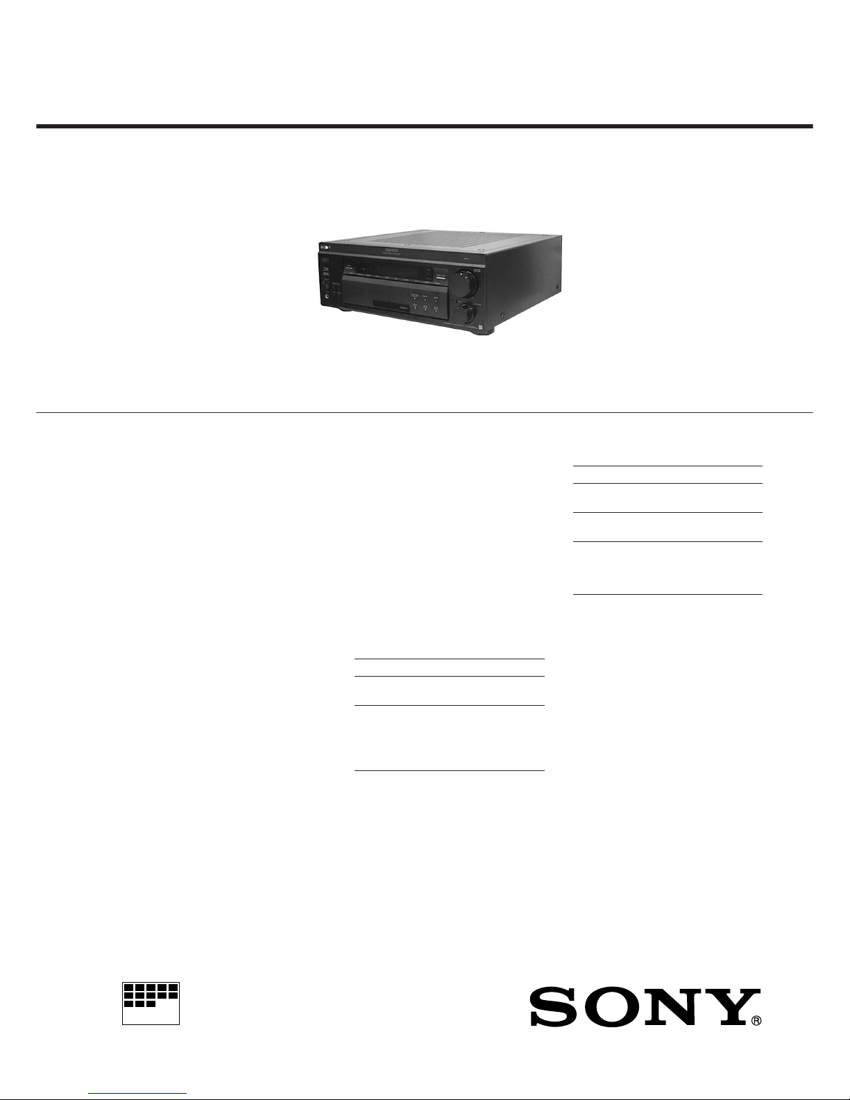
FM STEREO/FM-AM RECEIVER
MICROFILM
US Model
Canadian Model
Australian Model
Audio power specificaitons
POWER OUTPUT AND TOTAL
HARMONIC DISTORTION
With 8-ohm loads both channels
driven, from 20 - 20,000 Hz; rated 120
watts per channel minimum RMS
power, with no more than 0.05 % total
harmonic distortion from 250 miliwatts
to rated output (US model only).
Amplifier section
POWER OUTPUT
Stereo mode 8 ohms 20 Hz - 20 kHz,
THD 0.05 %,
120 W + 120 W
Surround mode (8 ohms at 1 kHz, THD
0.05 %)
Front: 120 W + 120 W
Center*: 120 W
Rear*: 120 W + 120 W
* No sound may be out-
put when using certain
sound sources and/or
sound mode settings.
SPECIFICATIONS
SERVICE MANUAL
STR-DA90ESG
Manufactured under license from Dolby
Laboratories Licensing Corporation.
“Dolby , ” the double-D symbol a, “AC-3” and
“Pro Logic” are trademarks of Dolby Laboratories Licensing Corporation.
Dynamic power 165 W + 165 W, 8 ohms
output (US, 280 W + 280 W, 4 ohms
Canadian model)
Harmonic Less than 0.05 %
distortion at (Direct Pass)
rated output
Frequency PHONO: RIAA
response equalization curve
±0.5 dB
CD, TAPE, DAT/MD,
LD, DVD, TV/DBS,
VIDEO: 10 Hz - 50
kHz dB
(Direct Pass)
Input (ANALOG)
Sensitivity Impedance S/N
PHONO 2.5 mV 50 75 dB*
kilohms (A, 2.5 mV)
CD, T APE,
DAT/MD,
VIDEO, 200 mV 50 82 dB*
LD/DVD, kilohms (A, 200mV)
TV/DBS
+0.5
–2
Input (DIGITAL)
Sensitivity Impedance S/N
LD/DVD – 75 ohms 100 dB
AC-3 RF (A, 20 kHz LPF)
LD/DVD – 75 ohms 100 dB
COAXIAL (A, 20 kHz LPF)
LD/DVD,CD,
DAT/MD, – – 100 dB
TV/DBS, (A, 20 kHz LPF)
OPTICAL
* '78 IHF
Outputs REC OUT:
DAT/MD, T APE
Voltage: 200 mV
Impedance: 1 kilohms
AUDIO OUT:
VIDEO 1, 2
Voltage: 200mV
Impedance: 1 kilohms
PRE OUT
Voltage: 2V
Impedance: 1 kilohms
PHONES: Accepts low
and high impedance
headphones
BASS BOOST +6 dB at 70 Hz
– Continued on page 2 –

– 2 –
Digital Signal Processor section
Modulation High Density Linear
(A/D conversion) Converter
Demodulation High Density Linear
(D/A conversion) Converter (Advanced
Pulse D/A converter)
Sampling 48 kHz
frequency
Surround LFE MIX
MUTE, –20 ~ 0 dB, 0.5
dB step
D.RANGE COMP
OFF, 0.1 ~ 0.9, STD,
MAX
REAR level
–20 ~ +10 dB, 0.5 dB
step
CENTER level
–20 ~ +10 dB, 0.5 dB
step
SUB WOOFER level
–20 ~ +10 dB, 0.5 dB
step
WALL
17-step adjustable
SEAT
L/R 17-step adjustable
F/R 17-step adjustable
EFFECT
21-step adjustable
REVERB time
17-step adjustable
Equalizer Band
BASS/TREBLE
Turnover frequency
BASS: 99 Hz ~ 992 Hz
TREBLE: 1.0 kHz ~
8.6 kHz
Level
±10 dB, 0.5 dB step
+0.5
–2
FM tuner section
Tuning range 87.5 - 108.0 MHz
Antenna 75 ohms, unbalanced
terminals
Sensitivity Mono: 18.3 dBf, 4.5 µV
Stereo: 38.3 dBf, 45 µV
Usable sensitivity 11.2 dBf, 2 µV (IHF)
S/N Mono: 76 dB
Stereo : 70 dB
Harmonic Mono: 0.3 %
distortion at Stereo: 0.5 %
1 kHz
Separation 45 dB at 1 kHz
Frequency 30 Hz - 15 kHz dB
response
Selectivity 60 dB at 400 kHz
AM tuner section
Tuning range With 10 kHz interval*:
530 - 1710 kHz
US, Canadian model
With 9 kHz interval:
531 - 1710 kHz
US, Canadian model
531 - 1602kHz
Australian model
Antenna Loop antenna
Usable sensitivity 50 dB/m (at 1,000 kHz or
999 kHz)
S/N 54 dB (at 50 mV/m)
Harmonic 0.5 % (50 mV/m,
distortion 400 kHz)
Selectivity At 9 kHz: 35 dB
At 10 kHz: 40 dB
* You can change the AM tuning interval be-
tween 9 kHz and 10 kHz. After tuning in any
AM station, turn off the receiver. While holding down the PRESET + button, press the
POWER switch. When you change the interval, all the preset stations will be erased. To
reset the interval, repeat the same procedure.
US, Canadian model
Video section
Inputs VIDEO:
1 Vp-p 75 ohms
S-VIDEO:
Y: 1 Vp-p 75 ohms
C: 0.286 Vp-p 75 ohms
Outputs VIDEO:
1 Vp-p 75 ohms
S-VIDEO:
Y: 1 Vp-p 75 ohms
C: 0.286 Vp-p 75 ohms
General
System Tuner section:
PLL quartz-locked
digital synthesizer system
Preamplifier section:
Low-noise NF type
equalizer
Power amplifier section:
Pure-complimentary
Parallel P.P.
Power Australian models:
requirements 240 V AC, 50 Hz
US, Canadian models:
120 V AC, 60 Hz
Power Australian models: 430 W
consumption US models: 385 W
Canada models: 550 VA
AC outlets Australian models:
1 switched, total 100 W
US, Canadian models:
2 switched, total 120 W
Dimensions 430 × 160 × 435 mm
(17 × 6
3
/8 × 171/4 inches)
Mass (Approx.) 16.0 kg (35 lb 4 oz)
Supplied • FM wire antenna (1)
accessories • AM loop antenna (1)
• Remote commander
(remote) (1)
(remote for US and
Canadian models:
RM-H501)
(Remote for Australian
model: RM-VR101)
• Size AA (R6) batteries
(2)
• IR repeater (1)
Design and specifications are subject to change
without notice.
– 3 –
TABLE OF CONTENTS
1. GENERAL
................................................................... 4
2. DISASSEMBLY.......................................................... 5
3. ELECTRICAL ADJUSTMENTS ......................... 7
4. DIAGRAMS
4-1. IC Pin Function Description ............................................ 9
4-2. Printed Wiring Boards – DISPLAY Section –................ 27
4-3. Schematic Diagram – DISPLAY Section – .................... 31
4-4. Schematic Diagram – VIDEO Section – ......................... 36
4-5. Printed Wiring Boards – VIDEO Section –.................... 41
4-6. Schematic Diagram
– INPUT/TUNER/POWER Section –............................. 45
4-7. Printed Wiring Boards
– INPUT/TUNER/POWER Section –............................. 49
4-8. Schematic Diagram – DIGITAL Section –...................... 54
4-9. Printed Wiring Board – DIGITAL Section –.................. 59
4-10. Schematic Diagram – AMP/OUTPUT Section – ............ 63
4-11. Printed Wiring Boards – AMP/OUTPUT Section –....... 67
5. EXPLODED VIEWS ................................................ 75
6. ELECTRICAL PARTS LIST................................ 79
SAFETY-RELATED COMPONENT WARNING!!
COMPONENTS IDENTIFIED BY MARK ! OR DOTTED LINE
WITH MARK ! ON THE SCHEMATIC DIAGRAMS AND IN
THE PARTS LIST ARE CRITICAL TO SAFE OPERATION.
REPLACE THESE COMPONENTS WITH SONY PAR TS WHOSE
PART NUMBERS APPEAR AS SHOWN IN THIS MANUAL
OR IN SUPPLEMENTS PUBLISHED BY SONY.
ATTENTION AU COMPOSANT AYANT RAPPORT
À LA SÉCURITÉ!
LES COMPOSANTS IDENTIFIÉS P AR UNE MARQUE ! SUR
LES DIAGRAMMES SCHÉMATIQUES ET LA LISTE DES
PIÈCES SONT CRITIQUES POUR LA SÉCURITÉ DE
FONCTIONNEMENT. NE REMPLACER CES COM- POSANTS
QUE P AR DES PIÈCES SONY DONT LES NUMÉR OS SONT
DONNÉS DANS CE MANUEL OU DANS LES SUPPLÉMENTS
PUBLIÉS PAR SONY.
MODEL IDENTIFICATION
– BACK PANEL –
US Model : 0
π
Canadian Model : 1
π
Australian Model : 2
π
SAFETY CHECK-OUT
After correcting the original service problem, perform the following safety check before releasing the set to the customer:
Check the antenna terminals, metal trim, “metallized” knobs,
screws, and all other exposed metal parts for AC leakage.
Check leakage as described below.
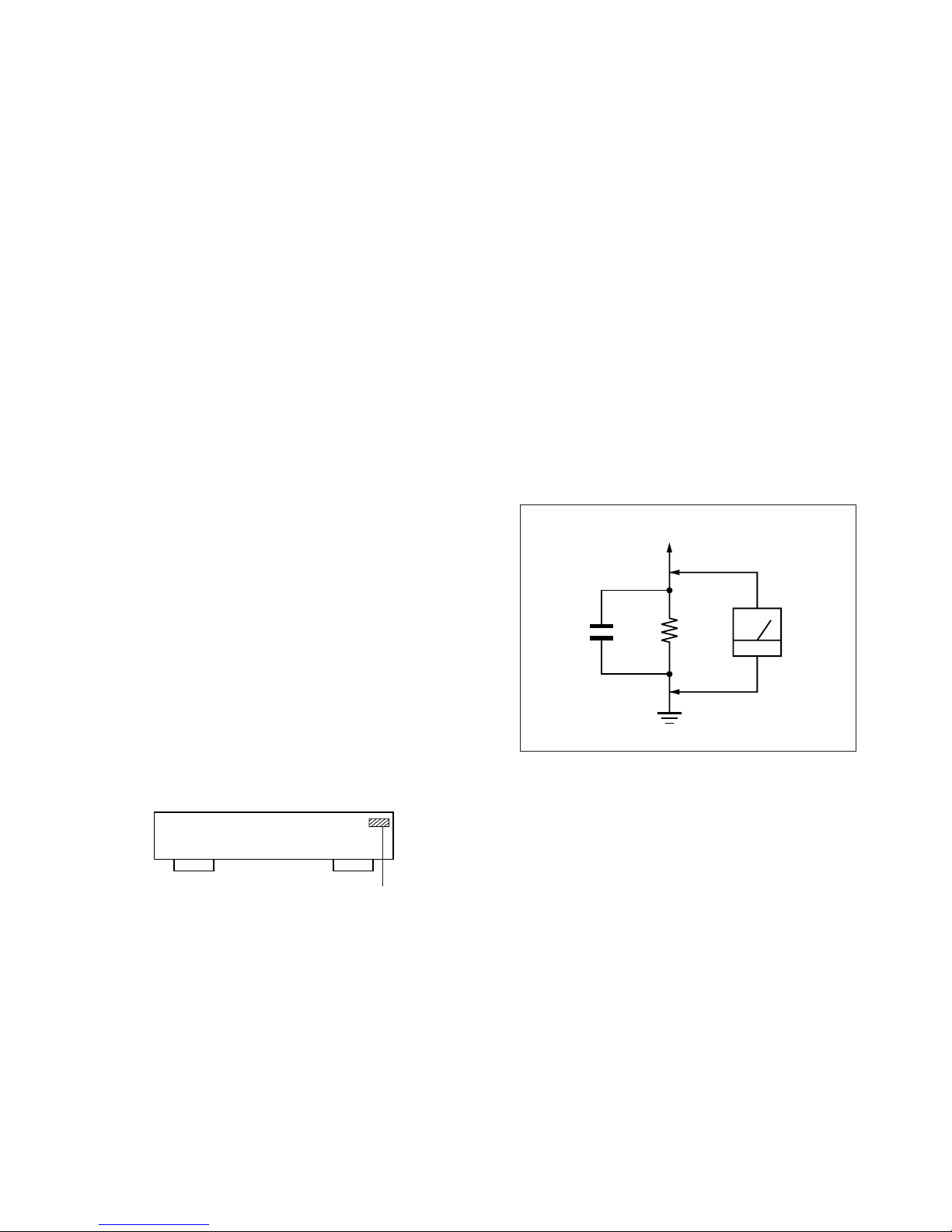
LEAKAGE TEST
The AC leakage from any exposed metal part to earth ground and
from all exposed metal parts to any exposed metal part having a
return to chassis, must not exceed 0.5 mA (500 microampers.).
Leakage current can be measured by any one of three methods.
1. A commercial leakage tester , such as the Simpson 229 or RCA
WT -540A. Follo w the manufacturers’ instructions to use these
instruments.
2. A battery-operated AC milliammeter. The Data Precision 245
digital multimeter is suitable for this job.
3. Measuring the voltage drop across a resistor by means of a
VOM or battery-operated AC voltmeter. The “limit” indication is 0.75 V, so analog meters must have an accurate lowvoltage scale. The Simpson 250 and Sanwa SH-63T rd are examples of a passive VOM that is suitable. Nearly all battery
operated digital multimeters that have a 2 V A C range are suitable. (See Fig. A)
Fig. A. Using an AC voltmeter to check AC leakage.
1.5 k
Ω
0.15 µF
AC
voltmeter
(0.75 V)
To Exposed Metal
Parts on Set
Earth Ground
4-991-373-
– 4 –
This section is extracted from
instruction manual.
SECTION 1
GENERAL
– 5 –
Note: Follow the disassembly procedure in the numerical order given.
CASE
SECTION 2
DISASSEMBLY
REAR PANEL SECTION
1
three screws
(M 3
×
8)
1
two screws
(M 3
×
8)
1
three screws
(M 3
×
8)
1
two screws
(M 3
×
8)
2
3
case
2
2
four screws
(BVTP 3
×
8)
1
connector
(CNV902)
1
connector
(CNE910)
1
connector
(CND802)
1
connector
(CNE807)
1
connector
(CND3503)
2
seven screws
(BVTP 3
×
8)
2
ten screws
(BVTP 3
×
8)
2
seven screws
(BVTP 3
×
8)
2
screw
(BVTP 3
×
8)
4
back panel section
3
two screws
(BVTP 3
×
6)
– 6 –
TUNER/AUDIO/SPTM BOARD, FRONT PANEL SECTION
INPUT BOARD
1
connector
(CNE211)
7
four screws
(BVTP 3
×
8)
1
five connectors
(
CND621, CNE601, 602,
)
CNV615, 616
8
front panel section
2
SPTM board
5
connector
(CNS201)
6
TUNER board
7
three screws
(BVTP 3
×
8)
4
flat wire
(CNS3503)
3
AUDIO board
1
connector
(CNS210)
1
connector
(CNS623)
1
connector
(CNV613)
2
five screws
(BVTP 3
×
8)
1
connector
(CNE939)
2
screw
(BVTP 3
×
8)
4
INPUT board
3
claw
1
five connectors
(
CNE601, 620, 622, 3501,
)
CNP202
– 7 –
SECTION 3
ELECTRICAL ADJUSTMENTS
ON SCREEN SECTION
OSD ADJUSTMENT
Setting:
Monitor TV
Vectroscope
VIDEO output terminal
SET
VIDEO 1 S terminal
S. VIDEO SG
Procedure:
1. Connect the frequency counter to R813.
2. T urn the PO WER switch ON, pr ess VIDEO 1 and set the function to VIDEO 1. (The input signal set to OFF.)
3. Turn the POWER switch OFF, keep the BAND ,
buttons
depressed at the same time and then turn the POWER switch
ON.
4. Check that the screen shown only the color bars, and then adjust CT802 so that the reading becomes 3.5796 MHz ± 10 kHz.
5. Adjust CT801 so that the right edge of the color bars on the
screen comes within the frame.
BLACK
RED
BLUE
DARK GRAY
GRAY
ORANGE
GREEN
WHITE
Center
a=b
(Picture of monitor screen)
ab
6. The input signal set to ON.
BLACK
(THROUGH)
BLUE
DARK GRAY
GRAY
(THROUGH)
GREEN
WHITE
R813
CT802
IC814
RV801 CT801
CT803
IC805
Frequency counter
7. Turn the POWER switch OFF, keep the BAND , buttons
depressed at the same time and then turn the POWER switch
ON.
8. Adjust the picture frame as shown in (picture of monitor screen)
when using a color bar chart for adjustment with RV801.
INITIALIZATION OF THE MICROCOMPUTER
KEEP the DISPLA Y , OPEN/CLOSE b uttons depressed simultaneously and then turn the POWER switch ON.
Adjustment Location: VIDEO board (Component side)
– 8 –
DC BIAS CURRENT Adjustment
(with no signal input)
Note:
1. DC BIAS CURRENT adjustments should be made 30 seconds after
the [POWER] switch is turned on (POWER ON).
2. After replacing the power transistors, DC BIAS CURRENT adjustments
should be perfomed.
Procedure:
Digital voltmeter
+
–
1
2
3
R615
R665
R016
R715
R765
AMP BOARD
[AMP BOARD] (COMPONENT SIDE)
R665
RV651
1
2
3
D973
D971
D972
C987
C988
C985
C986
1
2
3
R668
R765
RV751
R017
RV001
R016
R715
RV701
R718
R615
RV601
R618
3
2
1
32
1
2
3
FRONT Rch
REAR Rch
FRONT Lc
h
REAR Lch
CENTER
R768
1
Connecting Adjustment Reading on
point part Digital voltmeter
FRONT Lch R615 RV601 20 mV
FRONT Rch R665 RV651 20 mV
CENTER R016 RV001 20 mV
REAR Lch R715 RV701 20 mV
REAR Rch R765 RV751 20 mV
AMPLIFIRE SECTION
– 9 –
Pin No. Pin Name I/O Function
1 MBUS (VZ) I
Not used (fixed at “L”)
2 MBUS (MON) I
Not used (fixed at “L”)
3 MBUS (STU) O
Not used (open)
4 LED-V3 O
LED drive signal output terminal “H”: LED on (for function VIDEO 3 indicator)
5 LED-V2 O
LED drive signal output terminal “H”: LED on (for function VIDEO 2 indicator)
6 LED-V1 O
LED drive signal output terminal “H”: LED on (for function VIDEO 1 indicator)
7 STANDBY O
LED drive signal output terminal “H”: LED on Not used (open)
8 DPC (SURR) O
LED drive signal output terminal “H”: LED on (for SUR indicator)
9 DPC (EQ) O
LED drive signal output terminal “H”: LED on (for EQ indicator)
10 DPC (INDEX) O
LED drive signal output terminal “H”: LED on (for INDEX indicator)
11 DVSS —
Ground terminal
12 LED-CE O
LED drive signal output terminal “H”: LED on (for function CD indicator)
13 LED-DAT/MD O
LED drive signal output terminal “H”: LED on (for function DAT/MD indicator)
14 LED-TAPE O
LED drive signal output terminal “H”: LED on (for function TAPE indicator)
15 LED-TV O
LED drive signal output terminal “H”: LED on (for function TV/DBS indicator)
16 LED-LD O
LED drive signal output terminal “H”: LED on (for function LD/DVD indicator)
17 LED-V3 O
LED drive signal output terminal “H”: LED on (for function VIDEO 3 indicator)
18 LED-V2 O
LED drive signal output terminal “H”: LED on (for function VIDEO 2 indicator)
19 LED-V1 O
LED drive signal output terminal “H”: LED on (for function VIDEO 1 indicator)
20 RX (SIN) I
Receive data input from the on screen display controller (IC809)
21 TX (SOUT) O
Transmit data output to the on screen display controller (IC809)
22 BUSY I
Busy signal input from the on screen display controller (IC809)
23 FL CLEAR O
Display clear signal output to the fluorescent indicator tube driver (IC101, 102)
24 FL DATA O
Serial data output to the fluorescent indicator tube driver (IC102)
25 FL CLK O
Serial data transfer clock signal output to the fluorescent indicator tube driver (IC101, 102)
26 LAT (OSD) O
Serial data latch pulse signal output to the fluorescent indicator tube driver (IC101, 102)
27 SIRCS1 I
Sircs signal input from the remote control receiver (IC104)
28 AVCC —
Power supply terminal (+5V)
29 AVR+ I
Reference voltage input terminal (+5V)
30 AVR– I
Reference voltage input terminal (+0V)
31 GND —
Ground terminal
32 AD KEY IN 1 I
Key input terminal (A/D input)
S132 to 134 (INPUT MODE, DIRECT PASS, BASS BOOST keys)
33 AD KEY IN 2 I
Key input terminal (A/D input)
S116 to 119 (FM/AM, SHIFT, PRESET TUNING –/+ keys)
34 DVSS —
Ground terminal
35 AD KEY IN 3 I
Key input terminal (A/D input) S109 to 110 (EQUALIZER BAND, TUNING +/–, FM
MODE, MEMORY, DISPLAY keys)
36 AD KEY IN 4 I
Key input terminal (A/D input) S101 to 108 (EQUALIZER CH, DPC MODE,
cursor ←/↓/↑/→, SET UP, OPEN/CLOSE keys)
37 AD KEY IN 5 I
Key input terminal (A/D input)
S129 to 131 (MODE, SOUND FIELD ON/OFF, GENRE keys)
38 AD VERSION I
Setting terminal for the destination (A/D input)
39 VOL-UP I
Motor drive signal input for the master volume
40 VOL-DOWN I
Motor drive signal input for the master volume
41 MODE0 I
Mode selection terminal (fixed at “H”)
DISPLAY BOARD IC105 MB90673PF-G-206-BND
(FLUORESCENT INDICATOR TUBE DRIVE CONTROLLER, KEY CONTROL)
SECTION 4
DIAGRAMS
4-1. IC PIN FUNCTION DESCRIPTION
– 10 –
Pin No. Pin Name I/O Function
42 MODE1 I
Mode selection terminal (fixed at “H”)
43 MODE2 I
Mode selection terminal (fixed at “L”)
44 STANDBY I
Hardware standby signal input terminal (fixed at “H”)
45 STOP I
Stop signal input terminal
46 U-RESET I
System reset signal input from the master controller (IC3413) “L”: reset
47 U-SREQ O
Communication request signal output to the master controller (IC3413)
48 U-MREQ I
Communication request signal input from the master controller (IC3413)
49 U-DATA I/O
Serial data in/out with the master controller (IC3413)
50 U-CLOCK I
Serial data reading clock signal input from the master controller (IC3413)
51 HIFI/ES I
Setting terminal for the destination (fixed at “H”)
52 AUBUS-IN I
Audio bus signal input terminal
53 AUBUS-OUT O
Audio bus signal output terminal
54
FUNCTION-B
I
Jog dial pulse input of the rotary encoder (RV101 FUNCTION)
55 FUNCTION-A I
Jog dial pulse input of the rotary encoder (RV101 FUNCTION)
56 OUT-OPEN O
Motor drive signal output to the door open/close motor drive (IC107)
57 OUT-CLOSE O
Motor drive signal output to the door open/close motor drive (IC107)
58 SW-OPEN I
Door open detect sensor (PH102) input terminal
59 SW-CLOSE I
Door close detect sensor (PH103) input terminal
60 — —
Not used (open)
61 SWBAL I
Balance volume on/off detect signal input terminal
62 RESET I
Reset signal input terminal “L”: reset
63 GND —
Ground terminal
64 XO O
System clock signal output terminal (4MHz)
65 XI I
System clock signal input terminal (4MHz)
66 VCC —
Power supply terminal (+5V)
67 LED-TUNER O
LED drive signal output terminal “H”: LED on (for function TUNER indicator)
68 LED-PHONO O
LED drive signal output terminal “H”: LED on (for function PHONO indicator)
69 LED MUTE O
LED drive signal output terminal “H”: LED on (for MUTING indicator)
70
LED-LEARNING
O
LED drive signal output terminal “H”: LED on Not used (open)
71 LED D.PASS O
LED drive signal output terminal “H”: LED on (for DIRECT PASS indicator)
72 LED-INPUT O
LED drive signal output terminal “H”: LED on Not used (open)
73 LED VOL O
LED drive signal output terminal “H”: LED on (for MASTER VOLUME illumination)
74 LED BASS.B O
LED drive signal output terminal “H”: LED on (for BASS BOOST indicator)
75 SP-A I
Speaker select switch (S135) input terminal “H”: speaker A on
76 SP-B I
Speaker select switch (S135) input terminal “H”: speaker B on
77 PW-SW I
Power switch (S137) input terminal
78 LED-TV O
LED drive signal output terminal “H”: LED on (for function TV/DBS indicator)
79 LED-LD O
LED drive signal output terminal “H”: LED on (for function LD/DVD indicator)
80 — I
Not used (fixed at “L”)
– 11 –
S VIDEO BOARD IC809 MB90T673PF-G-BND (ON SCREEN DISPLAY CONTROLLER)
Pin No. Pin Name I/O Function
1 AD14 I/O
2 AD15 I/O
3 A16 O
4 A17 O
Address signal output to the program RAM (IC820)
5 A18 O
6 A19 O
Chip enable signal output to the program RAM (IC820) and S-RAM (IC821, 822)
7 PCE O
Chip enable signal output to the RC controller (IC815)
8 PCLK O
Serial data transfer clock signal output to the RC controller (IC815)
9 PDATA-OUT O
Serial data output to the RC controller (IC815)
10 PDATA-IN I
Serial data input from the RC controller (IC815)
11 GND —
Ground terminal
12 ALE O
Address latch enable signal output to the interface latch (IC816, 818)
13 RDX O
Read strobe signal output to the program RAM (IC820) and S-RAM (IC821, 822)
14 WRLX O
Write strobe signal output to the S-RAM (IC821) (for lower 8 bit)
15 WRHX O
Write strobe signal output to the S-RAM (IC822) (for higher 8 bit)
16 CTR-S-MON O
Not used (open)
17 CNT-S-V2 O
Not used (open)
18 CTR-S-OUT O
Not used (open)
19 CTR-S-V1 O
Not used (open)
20 RX (SIN) I
Receive data input from the FL drive controller (IC105)
21 TX (SOUT) O
Transmit data output to the FL drive controller (IC105)
22 RES O
Reset signal output to the RC controller (IC815) “L”: reset
23 — —
Not used (open)
24 DATA (OSD) O
Serial data output to the MB90095PF-G (IC805)
25 CLK (OSD) O
Serial data transfer clock signal output to the MB90095PF-G (IC805)
26 LAT (OSD) O
Serial data latch pulse signal output to the MB90095PF-G (IC805)
27 — —
Not used (open)
28 AVCC —
Power supply terminal (+5V)
29 AVR+ I
Reference voltage input terminal (+5V)
30 AVR– I
Reference voltage input terminal (+0V)
31 AVSS —
Ground terminal
32 VOL A/D I
A/D conversion input terminal for the volume (fixed at “L”)
33 XP-RS I
Data reception ready signal input from the RC controller (IC815)
34 GND —
Ground terminal
35 P-TDAT I
Infrared rays transmission data status signal input from the RC controller (IC815)
“H”: exist, “L”: nothing
36 P-OK I
Learning OK status signal input from the RC controller (IC815)
37 M FULL I
Memory full status signal input from the RC controller (IC815)
38 BACK UP NG I
Backup NG status signal input from the RC controller (IC815)
39 P-NG I
Learning NG status signal input from the RC controller (IC815)
40 P-IR I
Learn IR signal input terminal “H”: no signal
41 MODE0 I
Mode selection terminal (fixed at “H”)
42 MODE1 I
Mode selection terminal (fixed at “L”)
43 MODE2 I
Mode selection terminal (fixed at “L”)
44 HSTX I
Hardware standby signal input terminal (fixed at “H”)
45 STOP I
Stop signal input terminal
Two way data bus with the program ROM (IC820), S-RAM (IC822) and address data (for
address signal) output to the interface latch (IC818)
– 12 –
Pin No. Pin Name I/O Function
46 — —
Not used (open)
47 — —
Not used (open)
48 — —
Not used (open)
49 AUBUS-IN I
Audio bus signal input terminal
50 V.SIGNAL I
Video signal exist/without “H”: exist
51 SIRCS-IN I
Sircs signal input from the remote control receiver (IC104)
52 NTSC/PAL I
Detection signal input of the video system
53 AUBUS-OUT O
Audio bus signal output terminal
54
SCART (8)
O
Scart P8 control signal output terminal Not used (open)
55 SEETH O
See-through mode signal output terminal Not used (open)
56 — —
Not used (open)
57 — —
Not used (open)
58 — —
Not used (open)
59 — —
Not used (open)
60 IR-OFF O
IR on/off control signal output terminal
61 BUSY O
Busy signal output to the FL drive controller (IC105)
62 RESET I
Reset signal input terminal “L”: reset
63 GND —
Ground terminal
64 XO O
System clock signal output terminal (4MHz)
65 XI I
System clock signal input terminal (4MHz)
66 VCC —
Power supply terminal (+5V)
67 AD00 I/O
Two way data bus with the program ROM (IC820), S-RAM (IC821)
68 AD01 I/O
69 AD02 I/O
70 AD03 I/O
71 AD04 I/O
72 AD05 I/O
73 AD06 I/O
74 AD07 I/O
75 AD08 I/O
Two way data bus with the program ROM (IC820), S-RAM (IC822) and address data (for
address signal) output to the interface latch (IC818)
76 AD09 I/O
77 AD10 I/O
78 AD11 I/O
79 AD12 I/O
80 AD13 I/O
Two way data bus with the program ROM (IC820), S-RAM (IC822) and address data (for
address signal) output to the interface latch (IC818)
Two way data bus with the program ROM (IC820), S-RAM (IC821) and address data (for
address signal) output to the interface latch (IC816)
Two way data bus with the program ROM (IC820), S-RAM (IC821) and address data (for
address signal) output to the interface latch (IC818)
Two way data bus with the program ROM (IC820), S-RAM (IC822) and address data (for
address signal) output to the interface latch (IC816)
– 13 –
S VIDEO BOARD IC815 LC86F5864A-5F53 (RC CONTROLLER)
Pin No. Pin Name I/O Function
1CEI
Chip enable signal input from the on screen display controller (IC809)
2 INT1 I
Chip enable signal input terminal Not used (open)
3 INT2 I Not used (fixed at “L”)
4IRI
Learn IR signal input terminal “H”: no signal
5 STOP I Stop signal input terminal
6 DAT O
Infrared rays transmission data status signal output to the on screen display controller (IC809)
“H”: exist, “L”: noting
7NGO
Learning NG status signal output to the on screen display controller (IC809)
8 BACK UP NG O
Backup NG status signal output to the on screen display controller (IC809)
9 M FULL O
Memory full status signal output to the on screen display controller (IC809)
10 OK O
Learning OK status signal output to the on screen display controller (IC809)
11 RS O
Data reception ready signal output to the on screen display controller (IC809)
12 P37 O Not used (fixed at “L”)
13 P40 O Not used (fixed at “L”)
14 P41 O Not used (fixed at “L”)
15 P42 O Not used (fixed at “L”)
16 P43 O Not used (fixed at “L”)
17 P44 O Not used (fixed at “L”)
18 P45 O Not used (fixed at “L”)
19 P46 O Not used (fixed at “L”)
20 P47 O Not used (fixed at “L”)
21 SDA I/O Two-way data bus with the external EEPROM Not used (fixed at “L”)
22 SCL O Clock signal output to the external EEPROM Not used (fixed at “L”)
23 VSS2 —
Ground terminal
24 VDD2 —
Power supply terminal (+5V)
25 SDA I/O Two-way data bus with the external EEPROM Not used (fixed at “L”)
26 SCL O Clock signal output to the external EEPROM Not used (fixed at “L”)
27 TXD O Transmit data output terminal Not used (fixed at “L”)
28 RXD I Receive data input terminal Not used (fixed at “L”)
29 UCLK O Clock signal output terminal Not used (fixed at “L”)
30 P25 O Not used (fixed at “L”)
31 P26 O Not used (fixed at “L”)
32 P27 O Not used (fixed at “L”)
33 P00 O Not used (fixed at “L”)
34 P01 O Not used (fixed at “L”)
35 P02 O Not used (fixed at “L”)
36 P03 O Not used (fixed at “L”)
37 P04 O Not used (fixed at “L”)
38 P05 O Not used (fixed at “L”)
39 P06 O Not used (fixed at “L”)
40 P07 O Not used (fixed at “L”)
41 SO0 O
Serial data output to the on screen display controller (IC809)
42 SI0 I
Serial data input from the on screen display controller (IC809)
43 SCK0 I
Serial data reading clock signal input from the on screen display controller (IC809)
44 SO1 O
Serial data output terminal Not used (open)
45 SI1 I
Serial data input terminal Not used (open)
– 14 –
Pin No. Pin Name I/O Function
46 SCK1 I
Serial data reading clock signal input terminal Not used (open)
47 BUZ O Not used (fixed at “L”)
48 PWM O Sircs signal output terminal
49 TEST1 O Test terminal Not used (open)
50 RES I Reset signal input from the on screen display controller (IC809) “L”: reset
51 XT1 I Sub system clock input terminal Not used (fixed at “L”)
52 XT2 O Sub system clock output terminal Not used (open)
53 VSS1 —
Ground terminal
54 CF1 I Main system clock input terminal (6 MHz)
55 CF2 O Main system clock output terminal (6 MHz)
56 VDD1 —
Power supply terminal (+5V)
57 AN0 I Not used (fixed at “L”)
58 AN1 I Not used (fixed at “L”)
59 AN2 I Not used (fixed at “L”)
60 AN3 I Not used (fixed at “L”)
61 AN4 I Not used (fixed at “L”)
62 AN5 I Not used (fixed at “L”)
63 AN6 I Not used (fixed at “L”)
64 AN7 I Not used (fixed at “L”)
– 15 –
DIGITAL BOARD IC3308 SN-PM4007A (DOLBY (AC-3) DEMODULATOR)
Pin No. Pin Name I/O Function
1 GND —
Ground terminal
2 VDD —
Power supply terminal (+5V)
3 RESET I
Reset signal input from the master controller (IC3413) “L”: reset
4 OSCON I
Oscillation on/off control signal input terminal “H”: on (fixed at “H”)
5 DATA I
Test terminal Not used (fixed at “L”)
6 MCK I
Test terminal Not used (fixed at “L”)
7 MLTB I
Test terminal Not used (fixed at “L”)
8 IDST O
Test terminal Not used (open)
9 IDCK O
Test terminal Not used (open)
10 IDO O
Test terminal Not used (open)
11 TM0 I
Test terminal Not used (fixed at “L”)
12 ECCK O
Test terminal Not used (open)
13 DEY O
Test terminal Not used (open)
14 DRY O
Test terminal Not used (open)
15 DRY O
Test terminal Not used (open)
16 TM1 I
Test terminal Not used (fixed at “L”)
17 A0 O
18 A1 O
19 A2 O
20 A3 O
21 A4 O
22 A5 O
23 TM2 I
Test terminal Not used (fixed at “L”)
24 TM3 I
Test terminal Not used (fixed at “L”)
25 XOUT O
System clock output terminal Not used (open)
26 XIN I
System clock input terminal Not used (fixed at “L”)
27 NEXT I
Test terminal Not used (fixed at “L”)
28 GND —
Ground terminal
29 VDD —
Power supply terminal (+5V)
30 A6 O
Address signal output to the S-RAM (IC3309)
31 A7 O
Address signal output to the S-RAM (IC3309)
32 GND —
Ground terminal
33 VDD —
Power supply terminal (+5V)
34 A12 O
Address signal output to the S-RAM (IC3309)
35 A14 O
Address signal output to the S-RAM (IC3309)
36 WE O
Write enable signal output to the S-RAM (IC3309) “L” active
37 A13 O
38 A8 O
Address signal output to the S-RAM (IC3309)
39 A9 O
40 GND —
Ground terminal
41 A11 O
Address signal output to the S-RAM (IC3309)
42 OE O
Output enable signal output to the S-RAM (IC3309) “L” active
43 A10 O
Address signal output to the S-RAM (IC3309)
44 D7 I/O
45 D6 I/O
Address signal output to the S-RAM (IC3309)
Two-way data bus with the S-RAM (IC3309)
– 16 –
Pin No. Pin Name I/O Function
46 D5 I/O
47 D4 I/O
48 D3 I/O
49 D2 I/O
50 D1 I/O
51 D0 I/O
52 VDD —
Power supply terminal (+5V)
53 GND —
Ground terminal
54
TI1
I
Test terminal Not used (fixed at “H”)
55 VIN I
VCXO input terminal (18.432 MHz)
56 VOUT O
VCXO output terminal (18.432 MHz)
57 TI2 I
Test terminal Not used (fixed at “L”)
58 TI3 I
Test terminal Not used (fixed at “L”)
59 TLD8 I
Test terminal Not used (fixed at “L”)
60 TCK I
Test terminal Not used (fixed at “L”)
61 TRP O
Test terminal Not used (open)
62 TD0 O
Test terminal Not used (open)
63 PD0 O
Internal phase comparator output terminal
64 TI4 I
Test terminal Not used (fixed at “L”)
65 PDD15 I
PDO out control signal input terminal “L”: on
66 MUT0 O
Mute control signal output terminal “H”: mute on
67 TI5 I
Test terminal Not used (fixed at “L”)
68 VLDY O
Test terminal Not used (open)
69 DASYO O
Test terminal Not used (open)
70 DAOUT O
Digital out signal output terminal (serial data stream output)
71 DAIN I
Digital external input terminal Through out to DAOUT (pin &º) when DASEL (pin &™)is “H”
Not used (open)
72 DASEL I
Digital out selection terminal Fixed at “L”
73 TI8 I
Test terminal Not used (fixed at “L”)
74 C2F1 O
C2 error correction state monitor output terminal Outputs if corrected properly
Not used (open)
75 C2F0 O
C2 error correction state monitor output terminal Outputs number of errors at C2
Not used (open)
76 C1F1 O
C1 error correction state monitor output terminal Outputs whether error is present at C1
Not used (open)
77 C1F0 O
C1 error correction state monitor output terminal Outputs number of errors at C1
Not used (open)
78 MUT1 I
Mute signal input terminal “H”: mute
79 VDD —
Power supply terminal (+5V)
80 GND —
Ground terminal
81 AVDD —
Power supply terminal (+5V) (for analog system)
82 CPIN I
Comparator input (+) terminal
83 CMIN I
Comparator input (–) terminal
84 AGND —
Ground terminal (for analog system)
85 TM4 I
Test terminal Not used (fixed at “L”)
86 VDD —
Power supply terminal (+5V)
87 DIN I
Test terminal Not used (fixed at “L”)
Two-way data bus with the S-RAM (IC3309)
– 17 –
Pin No. Pin Name I/O Function
88 DOUT O
Comparator output terminal
89 DOUTB O
Comparator inverted output terminal
90 CSM O
Clock (9.216 MHz) output terminal Not used (open)
91 GND —
Ground terminal
92 WINGT O
Test terminal Not used (open)
93 SYST0 O
Test terminal Not used (open)
94 SYST1 O
Test terminal Not used (open)
95 ADST0 O
Test terminal Not used (open)
96 ADST1 O
Test terminal Not used (open)
97 TMS I
Test terminal Not used (fixed at “L”)
98 BUNR1 I
Test terminal Not used (fixed at “L”)
99 AGND —
Ground terminal (for analog system)
100 AVDD —
Power supply terminal (+5V) (for analog system)
– 18 –
DIGITAL BOARD IC3410 DSP56009FJ88F (DIGITAL SIGNAL PROCESSOR)
Pin No. Pin Name I/O Function
1 AGND —
Ground terminal (for address bus buffer)
2 MCS0 O
Chip select signal output to the external RAM device Not used (open)
3 MCS3 O
Chip select signal output to the external RAM device Not used (open)
4 MA14 O
Address signal output to the external RAM device Not used (open)
5 MA13 O
Address signal output to the external RAM device Not used (open)
6 AVCC —
Power supply terminal (+5V) (for address bus buffer)
7 MA12 O
Address signal output to the external RAM device Not used (open)
8 AGND —
Ground terminal (for address bus buffer)
9 QVCC —
Power supply terminal (+5V) (for internal logic)
10 QGND —
Ground terminal (for internal logic)
11 MA11 O
12 MA10 O
13 MA9 O
14 MA8 O
15 AGND —
Ground terminal (for address bus buffer)
16 MA7 O
Address signal output to the external RAM device Not used (open)
17 AVCC —
Power supply terminal (+5V) (for address bus buffer)
18 MA6 O
19 MA5 O
Address signal output to the external RAM device Not used (open)
20 MA4 O
21 AGND —
Ground terminal (for address bus buffer)
22 MA3 O
23 MA2 O
24 MA1 O
25 MA0 O
26 SCK I
Serial data reading clock signal input from the master controller (IC3413)
27 EXTAL I
Master clock signal input terminal (3MHz)
28 QVCC —
Power supply terminal (+5V) (for internal logic)
29 QGND —
Ground terminal (for internal logic)
30 PINIT I
Initialize input for the PLL circuit (fixed at “L”)
31 PGND —
Ground terminal (for PLL circuit)
32 PCAP I
Connected to the external capacitor for PLL circuit filter
33 PVCC —
Power supply terminal (+5V) (for PLL circuit)
34 SGND —
Ground terminal (for serial port)
35 MISO I
Communication data input from the master controller (IC3413)
36 RESET I
Reset signal input from the master controller (IC3413) “L”: reset
37 MODA I
Mode selection terminal (fixed at “H”)
38 MODB I
Mode selection terminal (fixed at “L”)
39 MODC I
Mode selection terminal (fixed at “H”)
40 SVCC —
Power supply terminal (+5V) (for serial port)
41 MOSI O
Communication data output to the master controller (IC3413)
42 SS I
SPI slave select signal input from the master controller (IC3413)
43 HREQ I
Host request signal input from the master controller (IC3413)
44 SGND —
Ground terminal (for serial port)
45 SDO2 O
Audio serial data output terminal Not used (open)
Address signal output to the external RAM device Not used (open)
Address signal output to the external RAM device Not used (open)
– 19 –
Pin No. Pin Name I/O Function
46 SDO1 O
Audio serial data output to the digital signal processor (IC3412)
47 SDO0 O
Audio serial data output to the digital signal processor (IC3412)
48 SVCC —
Power supply terminal (+5V) (for serial port)
49 SCKT O
Audio serial data transfer clock signal output to the digital signal processor (IC3412)
50 WST O
Word transmission output to the digital signal processor (IC3412)
51 SCKR I
Bit clock signal (2.8224 MHz) input terminal
52 QGND —
Ground terminal (for internal logic)
53 QVCC —
Power supply terminal (+5V) (for internal logic)
54
SGND
—
Ground terminal (for serial port)
55 WSR I
L/R sampling clock signal (44.1 kHz) input terminal
56 SDI1 I
Audio serial data input terminal
57 SDI0 I
Audio serial data input terminal
58 DSO O
Debug serial data output terminal Not used (open)
59 DSI I
Debug serial data input terminal Not used (open)
60 DSCK I
Debug serial data reading clock signal input terminal Not used (open)
61 DR I
Debug request signal input terminal Not used (fixed at “H”)
62 MD7 I/O
63 MD6 I/O
64 MD5 I/O
65 MD4 I/O
66 DGND —
Ground terminal (for data bus buffer)
67 MD3 I/O
68 MD2 I/O
Two-way data bus with the external RAM device Not used (open)
69 MD1 I/O
70 DVCC —
Power supply terminal (+5V) (for data bus buffer)
71 MD0 I/O
Two-way data bus with the external RAM device Not used (open)
72 DGND —
Ground terminal (for data bus buffer)
73 GPIO3 I/O
74 GPIO2 I/O
75 GPIO1 I/O
76 GPIO0 I/O
77 MRD O
Write strobe signal output to the external RAM device Not used (open)
78 MWR O
Read strobe signal output to the external RAM device Not used (open)
79 MRAS O
Row address strobe signal output to the external RAM device Not used (open)
80 MCAS O
Column address strobe signal output to the external RAM device Not used (open)
Two-way data bus with the external RAM device Not used (open)
General digital signal processor in/out terminal Not used (open)

– 20 –
DIGITAL BOARD IC3412 SSP424023FJ88 (DIGITAL SIGNAL PROCESSOR)
Pin No. Pin Name I/O Function
1 AGND —
Ground terminal (for address bus buffer)
2 MCS0 O
Chip select signal output to the external RAM device Not used (open)
3 MA15 O
4 MA14 O
Address signal output to the S-RAM (IC3411)
5 MA13 O
6 AVCC —
Power supply terminal (+5V) (for address bus buffer)
7 MA12 O
Address signal output to the S-RAM (IC3411)
8 AGND —
Ground terminal (for address bus buffer)
9 QVCC —
Power supply terminal (+5V) (for internal logic)
10 QGND —
Ground terminal (for internal logic)
11 MA11 O
12 MA10 O
13 MA9 O
14 MA8 O
15 AGND —
Ground terminal (for address bus buffer)
16 MA7 O
Address signal output to the S-RAM (IC3411)
17 AVCC —
Power supply terminal (+5V) (for address bus buffer)
18 MA6 O
19 MA5 O
Address signal output to the S-RAM (IC3411)
20 MA4 O
21 AGND —
Ground terminal (for address bus buffer)
22 MA3 O
23 MA2 O
24 MA1 O
25 MA0 O
26 SCK I
Serial data reading clock signal input from the master controller (IC3413)
27 EXTAL I
Master clock signal input terminal (3MHz)
28 QVCC —
Power supply terminal (+5V) (for internal logic)
29 QGND —
Ground terminal (for internal logic)
30 PINIT I
Initialize input for the PLL circuit (fixed at “L”)
31 PGND —
Ground terminal (for PLL circuit)
32 PCAP I
Connected to the external capacitor for PLL circuit filter
33 PVCC —
Power supply terminal (+5V) (for PLL circuit)
34 SGND —
Ground terminal (for serial port)
35 MISO I
Communication data input from the master controller (IC3413)
36 RESET I
Reset signal input from the master controller (IC3413) “L”: reset
37 MODA I
Mode selection terminal (fixed at “H”)
38 MODB I
Mode selection terminal (fixed at “L”)
39 MODC I
Mode selection terminal (fixed at “H”)
40 SVCC —
Power supply terminal (+5V) (for serial port)
41 MOSI O
Communication data output to the master controller (IC3413)
42 SS I
SPI slave select signal input from the master controller (IC3413)
43 HREQ I
Host request signal input from the master controller (IC3413)
44 SGND —
Ground terminal (for serial port)
45 SDO2 O
Audio serial data output terminal (for rear side speaker)
Address signal output to the S-RAM (IC3411)
Address signal output to the S-RAM (IC3411)
– 21 –
Pin No. Pin Name I/O Function
46 SDO1 O
Audio serial data output terminal (for center side speaker)
47 SDO0 O
Audio serial data output terminal (for front side speaker)
48 SVCC —
Power supply terminal (+5V) (for serial port)
49 SCKT O
Bit clock signal (2.8224 MHz) output terminal
50 WST O
L/R sampling clock signal (44.1 kHz) output terminal
51 SCKR I
Audio serial data reading clock signal input from the digital signal processor (IC3410)
52 QGND —
Ground terminal (for internal logic)
53 QVCC —
Power supply terminal (+5V) (for internal logic)
54
SGND
—
Ground terminal (for serial port)
55 WSR I
Word transmission input from the digital signal processor (IC3410)
56 SDI1 I
Audio serial data input from the digital signal processor (IC3410)
57 SDI0 I
Audio serial data input from the digital signal processor (IC3410)
58 DSO O
Debug serial data output terminal Not used (open)
59 DSI I
Debug serial data input terminal Not used (open)
60 DSCK I
Debug serial data reading clock signal input terminal Not used (open)
61 DR I
Debug request signal input terminal Not used (fixed at “H”)
62 MD7 I/O
63 MD6 I/O
64 MD5 I/O
65 MD4 I/O
66 DGND —
Ground terminal (for data bus buffer)
67 MD3 I/O
68 MD2 I/O
Two-way data bus with the S-RAM (IC3411)
69 MD1 I/O
70 DVCC —
Power supply terminal (+5V) (for data bus buffer)
71 MD0 I/O
Two-way data bus with the S-RAM (IC3411)
72 DGND —
Ground terminal (for data bus buffer)
73 GPIO3 I/O
74 GPIO2 I/O
General digital signal processor in/out terminal Not used (open)
75 GPIO1 I/O
76 GPIO0 I/O
General digital signal processor in/out with the master controller (IC3413)
77 MRD O
Write strobe signal output to the S-RAM (IC3411)
78 MWR O
Read strobe signal output to the S-RAM (IC3411)
79 CS1 O
Chip select signal output to the external RAM device Not used (open)
80 MA16 O
Address signal output to the S-RAM (IC3411)
Two-way data bus with the S-RAM (IC3411)

– 22 –
1 RFERR I RF demodulater error signal input terminal “H”: error
2 RFRESET O RF demodulater reset signal output terminal “L”: active
3 STOP I System stop signal input terminal “L”: stop
4 RDATA I Data signal input from the digital audio interface receiver (IC3311)
5 WDATA O Data signal output to the digital audio interface receiver (IC3311)
6 DIRLAT O Latch pulse signal output to the digital audio interface receiver (IC3311)
7 DIRCLK O Clock signal output to the digital audio interface receiver (IC3311)
8 DIRERR I Error signal input from the digital audio interface receiver (IC3311)
9 ANG/DIG O Analog/Digital data select signal output to the selector (IC3414)
10 A/DINT O Initialize signal output to the A/D convertor (IC3104)
11 Vss — Ground terminal
12 HREQ I Host request signal input from the digital signal processor (IC3410)
13 SS O SPI slave select signal output to the digital signal processor (IC3410)
14 MOSI O Communication data output to the digital signal processor (IC3410)
15 RESET O Reset signal output to the digital signal processor (IC3410)
16 MISO I Communication data input from the digital signal processor (IC3410)
17 CLOCK O Serial data reading clock signal output to the digital signal processor (IC3410)
18 HREQ I Host request signal input from the digital signal processor (IC3412)
19 SS O SPI slave select signal output to the digital signal processor (IC3412)
20 MOSI O Communication data output to the digital signal processor (IC3412)
21 RESET O Reset signal output to the digital signal processor (IC3412)
22 MISO I Communication data input from digital signal processor (IC3412)
23 VCC — Power supply terminal (+5 V)
24 CLOCK O Serial data reading clock signal output to the digital signal processor (IC3412)
25 D/AINT O Initialize signal output to the digital filter (IC3401~3403)
26 D/ALAT O Latch pulse signal output to the digital filter (IC3401~3403)
27 C — Connect capacitor
28 D/ACLK O Serial data reading clock signal output to the digital filter (IC3401~3403)
29 D/ADATA O Data signal output to the digital filter (IC3401~3403)
30 SRCINI O Initialize signal output Not used (open)
31 D/A8DAT O 8bit data signal output to the D/A convertor Not used (open)
32 D/A8CLK O 8bit serial data reading clock signal output to the D/A convertor Not used (open)
33 D/A8LAT O 8bit latch pulse signal output to the D/A convertor Not used (open)
34, 35 VCC — Power supply terminal (+5 V)
36, 37 VSS — Ground terminal
38
LOW-FRQ-IED
I General digital signal input from digital signal processor (IC3412)
39
GAIN-FRONT-8DB
O Front out +8 dB signal output terminal “H”: active
40
GAIN-FRONT-4DB
O Front out +4 dB signal output terminal “H”: active
41
GAIN-FRONT-2DB
O Front out +2 dB signal output terminal “H”: active
42 VSS — Ground terminal
43 to 47 N.C. — Not used (open)
48 STOPIN I Power check signal input terminal “L”: error
49 MD0 I Mode set terminal (fixed at “H”)
50 MD1 I Mode set terminal (fixed at “H”)
51 MD2 I Mode set terminal (fixed at “L”)
• DIGITAL BOARD IC3413 MB90641APF-G-104-BND (MASTER CONTROLLER)
Pin No. Pin Name I/O Function
 Loading...