

Page 1
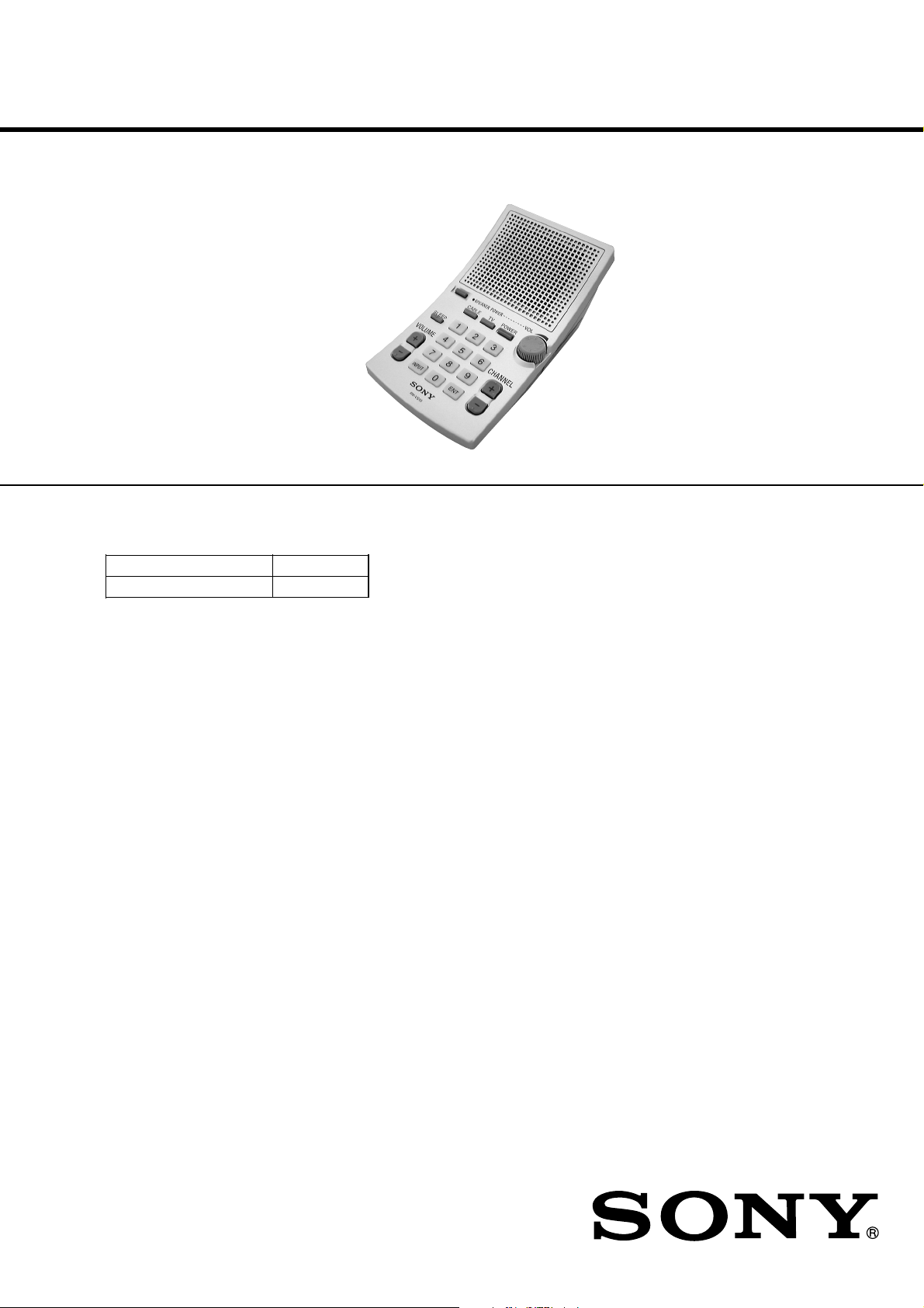
RM-VS10
SERVICE MANUAL
Ver 1.0 2000. 06
• RM-VS10 is the component model block one in RM-VS10TV.
COMPONENT MODEL NAME FOR RM-VS10TV
TRANSMITTER TMR-IF10M
REMOTE COMMANDER RM-VS10
US Model
General
Modulation system Frequency modulation
Carrier frequency 2.3 MHz (monaural)
Remote Commander RM-VS10
Power source Four size AA (R6) batteries (not supplied)/
external DC 4.5 V power sources (AC power
adaptor not supplied)
Maximum speaker output 0.8 W
Battery life (for 5 mW speaker output usage)
Approx. 20 hours (using Sony battery R6)
Approx. 60 hours (using Sony alkaline battery
LR6)
SPECIFICATIONS
Remote control operation distance
Approx. 7 m* (23 ft.) (when facing directly
toward the infrared receptor of your TV/analog
cable box)
Dimensions 93 × 86 × 158 mm (3 3/4 × 3 1/2 × 6 1/4 in.)
(w × h × d)
Mass Approx. 355 g (13 oz.) (including batteries)
* The distance may vary depending on using conditions and
the manufacturer and equipment that is used.
Design and specifications are subject to change without
notice.
Notes on Chip Component Replacement
• Never reuse a disconnected chip component.
• Notice that the minus side of a tantalum capacitor may be
damaged by heat.
SPEAKER REMOTE
COMMANDER SYSTEM
Page 2
0
SECTION 1
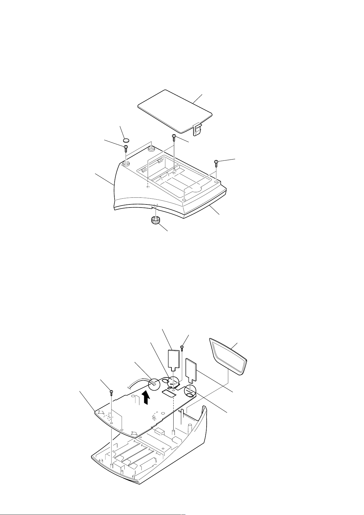
DISASSEMBLY
Note : Follow the disassembly procedure in the numerical order given.
1-1. CASE (RX), LOWER
5 foot (A), rubber
1 lid, battery case
6 BTP 2.6x10
7 case (RX), lower
1-2. FE, RM AND RX BOARDS
4 BTP 2.6x10
3 BTP 2.6x1
case assy (RX), upper
2 knob, volume
5 Removal the solders.
3 B 2.6x8
0 RX board
6 Removal the solder.
4
7 RM board
2 B 2.6x8
1 filter (RX)
9 FE board
8 Removal the solder.
– 2 –
Page 3
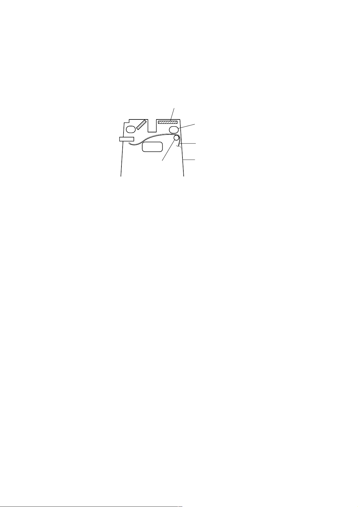
5
1-3. WIRING METHOD FOR RX BOARD
When assembling the RM-VS10, wire as shown in the figure below.
FE board
hole(boss)
install wire so as to be caught
between the hole(boss) and C7
C75
RX board
– 3 –
Page 4
SECTION 2
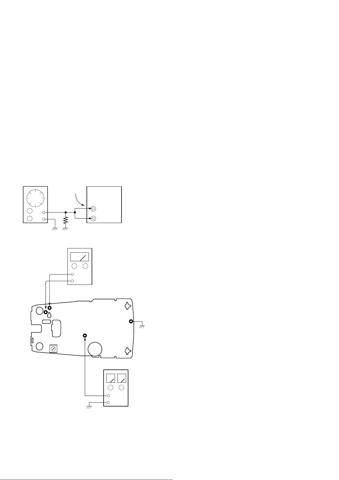
ELECTRICAL ADJUSTMENTS
Note:
1. The adjustments is performed in the order that they are listed.
2. When adjusting the remote commander, the transmitter is used
for adjustment.
3. 0 dB=1.0 V
2-1. Remote commander
2-1-1. Tuning adjustment
Method:
1. Supply 6 V to TP1 (6 V) from a stabilized power supply.
(TP3 (GND) is connected to the ground.)
2. Input a signal of 1 kHz and –10 dB to the transmitter (TMRIF10M) from an oscillator.
3. Connect a distortion factor meter between TP20 and TP21.
Note:The speaker should be always connected to protect the
circuit.
4. Set the volume (VR51) to the maximum position.
5. Adjust T51 so that the reading on the distortion factor
meter is minimum.
Connections and adjustment element:
Transmitter
Oscillator
AUDIO IN A
(TMR-IF10M)
1 kHz/
–10 dB
TP21
+
–
600 Ω
Distortion factor meter
+
–
– RX BOARD
(CONDUCTOR SIDE) –
TP20
TP1
T51
L
R
TP3
VR51
6Vdc
Stabilized power supply
+
–
– 4 –
Page 5

SECTION 3
DIAGRAMS
RM-VS10
3-1. BLOCK DIAGRAM
FE BOARD
B+
RF AMP
INFRARED
SENSOR
Q53-55
D53
RM BOARD
+
4.5V
INFRARED
EMITTER
D51
BUFFER
Q56
RX BOARD
16
MIXER LIMITER DEMOD
LED
DRIVER
Q52
OSC
X51
4MHz
3 5
T51
TUNING
SYSTEM CONTROL
8
REM
10
OSC2
11
OSC1
IC52
8
B+
FM DET
IC53
15
|
21
•
23
|
26
SQUELCH
TRIGGER,
HYSTERESIS
CARBON
SWITCH
THIS NOTE IS COMMON FOR PRINTED WIRING
BOARDS AND SCHEMATIC DIAGRAMS.
(In addition to this, the necessary note is
printed in each block.)
for Schematic Diagram:
• All capacitors are in µF unless otherwise noted. pF: µµF
AMP
VR51
9
13
14
MUTE
Q57
VOL
IC54
+
7
8
5
6
1
–
+
3
–
SP1
SPEAKER
J51
EARPHONE
50 WV or less are not indicated except for electrolytics
and tantalums.
• All resistors are in Ω and 1/
specified.
4
W or less unless otherwise
• % : indicates tolerance.
f
•
: internal component.
• C : panel designation.
• U : B+ Line.
• H : adjustment for repair.
• Power voltage is dc 4.5 V and fed with regulated dc power
supply from external power voltage jack.
• Voltage is dc with respect to ground under no-signal
+
3V REG
IC55
+
3V
3 2
REG
B+
D54
SPEAKER
POWER
POWER
SWITCH
Q58
+4.5V POWER
SWITCH
Q51
TIMER
IC51
7 6
CONTROL
+
4.5V
+4.5V
POWER
SWITCH
Q51
SPEAKER POWER
DC IN 4.5V
!
DRY BATTERY
UM-3X4
6V
J52
• Signal path
: ANALOG
: RF
(detuned) condition.
no mark : POWER on
• Voltages are tak en with a V OM (Input impedance 10 MΩ).
Voltage var iations may be noted due to normal production tolerances.
• Signal path.
F : Analog
J : RF
for Printed Wiring Boards:
• X : parts extracted from the component side.
• Y : parts extracted from the conductor side.
z
•
•
: Through hole.
f
: internal component.
• b : Pattern from the side which enables seeing.
(The other layer’s patterns are not indicated.)
Caution:
Pattern face side: Parts on the pattern face side seen from
(Conductor Side) the pattern face are indicated.
Parts face side: Parts on the carbon pattern face side
(Carbon Pattern seen from the carbon pattern face are
Side) indicated.
• IC BLOCK DIAGRAMS
IC53 MC3361CD IC51 BU2305F-E2
MIXER
INPUT
16
OSCILLATOR
1
CRYSTAL
OSC
MIXER
MUTE
GND
15
14
SQUELCH TRIGGER WITH
HYSTERESIS
2
MIXER
OUTPUT
3
SCAN
CONTROL
13
VCC
4
SQUELCH
IN
12
LIMITER
INPUT
5
FILTER
OUTPUT
FILTER
AMP
LIMITER
AMP
FILTER
INPUT
11
_
+
6
DECOUPLING
RECOVERED
AUDIO
10
AF
+
AMP
DEMODULATOR
+
7
QUAD
COIL
OSC1
9
8
1
23 BIT
COUNTER
OSC2
2
CONTROL
CHATTERING
PROECTOR
OSC3
3
4 5
GND
VDD
8
OUT
7
SET
6
RF
– 5 – – 6 –
Page 6

RM-VS10
3-2. PRINTED WIRING BOARDS • Refer to page 6 for Note.
A
B
C
D
1
2 3 4 5 6 7 8 9 10 11 12 13 14
RX BOARD (CARBON PATTERN SIDE)
SLEEP
VOLUME
SPEAKER
POWER
E
F
G
H
INPUT
ENT
CHANNEL
04
741
8520
963
CABLE
POWER
TV
1-678-157-
11
(11)
I
J
– 7 – – 8 –
Page 7

• Refer to page 6 for Note.
RM-VS10
234567891011121314
1
A
PD BOARD
J51
EARPHONE
J52
DC IN 4.5V
!
1-678-160-
11
(11)
RX BOARD
(CONDUCTOR SIDE)
TP19
EB
C59
C58
SP1
SPEAKER
Q52
C
AK
RED
WHT
TP21
R56
R55
RM BOARD
D51
INFRARED EMITTER
D51
A
K
1-678-159-
11
(11)
FE BOARD
B
S
G
TP11
TP13
C71
TP12
L53
C72
R63
C
C91
R78
C64
L51
C
TP6
Q55
C61
E
B
R58
C62
04
D53
D53
INFRARED SENSOR
• Semiconductor Location
Ref. No. Location Ref. No. Location
D51 E-14
D53 G-13
D54 D-7
D55 F-9
D56 F-10
IC51 E-8
IC52 D-4
IC53 G-9
IC54 H-5
IC55 D-6
L52
C90
G
TP7
C66
Q53
R61
D
S
C65
C
Q54
B
E
TP10
TP9
R59
C
Q56
E
B
R62
R60
1-678-158-
G
C67
TP8
Q51 G-6
Q52 D-11
Q53 G-13
Q54 G-13
Q55 G-13
Q56 G-13
Q57 H-8
Q58 G-10
Q59 D-8
S
B
11
(11)
SP+
WHT
SP-
R57
D56
TP14
C81
C73
E
16 9
Q58
R77
B
1
R74
BLK
TP15
C75
RED
C76
D55
IC53
C68
TP20
C69
R66
C78
8
C70
C74
C77
R64
RED
R65
TP18
321
46
R67
T51
R68 C80
C82
JC3
R79
C93
R52
TP4
R69
TP17
B
E
C
41
IC51
58
C54
BLK
C79
TP16
R73
C
Q57
Q59
C53
RED
R70
E
B
R51
R53
ORG
C60
D54
SPEAKER
POWER
C56
R71
TP2
123
IC55
C92
KA
TP1
C55
R54
B
E
C57
C51
Q51
C52
R72
C
TP5
JC1
VR51
VOL
X51
DRY BATTERY
UM-3x4
6V
1
JC2
C85
C84
8
C83
28 25 20
IC52
1 5 10 14
4
C86
C88
IC54
C87
5
R75
R76
15
TP3
11
1-678-157-
(11)
B
C
D
E
F
G
H
I
J
– 9 – – 10 –
Page 8

RM-VS10
3-3. SCHEMATIC DIAGRAM • Refer to page 5 for IC Block Diagram. Refer to page 6 for Note.
• Waveforms (When pressing the buttons on the commander)
0.1V/div
1
IC52 q; (OSC2) IC53 qa (FILTER-OUT)
0.1µsec/div
2.0Vp-p
4MHz
– 11 – – 12 –
2
0.1V/div
10µsec/div
2.0Vp-p
Page 9

NOTE:
• The mechanical parts with no reference
number in the exploded views are not supplied.
• Items marked “*” are not stocked since
they are seldom required for routine service.
Some delay should be anticipated
when ordering these items.
REMOTE COMMANDER SECTION
12
SECTION 4
EXPLODED VIEWS
• -XX and -X mean standardized parts, so
they may have some difference from the
original one.
• Color Indication of Appearance Parts
Example :
KNOB, BALANCE (WHITE) ... (RED)
SP1
14
13
20
11
5
R
Parts Color Cabinet’s Color
16
21
4
R
14
21
not
supplied
(PD board)
18
• Accessories and packing materials and
hardware (# mark) list are given in
the last of this parts list.
15
21
3
2
1
21
19
6
7
22
22
22
9
8
17
10
Ref. No. Part No. Description Remark Ref. No. Part No. Description Remark
* 1 A-4542-653-A RX BOARD, COMPLETE
* 2 A-4542-654-A FE BOARD, COMPLETE
* 3 1-678-159-11 RM BOARD
4 4-224-829-01 TERMINAL, BATTERY
5 4-224-830-01 SPRING (A), BATTERY
6 4-224-823-11 CASE (RX), LOWER
7 3-043-447-01 FOOT (B), RUBBER
8 4-224-831-01 SPRING (B), BATTERY
9 4-224-824-11 LID, BATTERY CASE
10 3-043-446-01 FOOT (A), RUBBER
13 4-224-827-01 KNOB, VOLUME
14 4-224-828-01 HOLDER, SPEAKER
15 4-224-825-01 FILTER (RX)
16 3-044-560-01 PACKING, LED
17 3-043-324-01 CUSHION, BATTERY
18 3-044-715-01 SEAL, SHIELD
19 3-045-142-01 PLATE, FE SHIELD
20 3-044-561-01 PACKING, VOLUME
21 7-685-534-14 SCREW +BTP 2.6X8 TYPE2 N-S
22 7-685-535-19 SCREW +BTP 2.6X10 TYPE2 N-S
11 4-224-826-11 SHEET, RUBBER KEY
12 X-3379-559-1 CASE ASSY (RX), UPPER
SP1 1-505-851-11 SPEAKER (057F014)
– 13 –
Page 10

SECTION 5
FE RX
NOTE:
• Due to standardization, replacements in
the parts list may be different from the
parts specified in the diagrams or the
components used on the set.
• -XX and -X mean standardized parts, so
they may have some difference from the
original one.
• RESISTORS
All resistors are in ohms.
METAL:Metal-film resistor.
METAL OXIDE: Metal oxide-film resistor.
F:nonflammable
Ref. No. Part No. Description Remark Ref. No. Part No. Description Remark
* A-4542-654-A FE BOARD, COMPLETE
RM
ELECTRICAL PARTS LIST
• Items marked “*” are not stocked since
they are seldom required for routine service.
Some delay should be anticipated
when ordering these items.
• SEMICONDUCTORS
In each case, u : µ, for example:
uA.. : µA.. uPA.. : µPA..
uPB.. : µPB.. uPC.. : µPC.. uPD.. : µPD..
• CAPACITORS
uF : µF
• COILS
uH : µH
(SUPPLIED WITH RX BOARD, COMPLETE)
*******************
When indicating parts by reference
number, please include the board.
* A-4542-653-A RX BOARD, COMPLETE (INCLUDING
FE BOARD, COMPLETE AND RM BOARD)
*******************
3-045-142-01 PLATE, FE SHIELD
< CAPACITOR >
C61 1-163-038-91 CERAMIC CHIP 0.1uF 25V
C62 1-163-038-91 CERAMIC CHIP 0.1uF 25V
C64 1-163-089-00 CERAMIC CHIP 6PF 50V
C65 1-163-021-91 CERAMIC CHIP 0.01uF 10% 50V
C66 1-163-021-91 CERAMIC CHIP 0.01uF 10% 50V
C67 1-163-038-91 CERAMIC CHIP 0.1uF 25V
C90 1-163-227-11 CERAMIC CHIP 10PF 0.5PF 50V
C91 1-163-222-11 CERAMIC CHIP 5PF 0.25PF 50V
< PHOTO SENSOR >
D53 8-719-058-49 PHOTO SENSOR PP508 (INFRARED SENSOR)
< COIL >
L51 1-412-213-21 INDUCTOR CHIP 150uH
L52 1-412-215-21 INDUCTOR CHIP 220uH
< TRANSISTOR >
Q53 8-729-220-93 FET 2SK209-G
Q54 8-729-026-49 TRANSISTOR 2SA1037AK-T146-R
Q55 8-729-120-28 TRANSISTOR 2SC1623-L5L6
Q56 8-729-026-49 TRANSISTOR 2SA1037AK-T146-R
< RESISTOR >
R58 1-216-057-00 METAL CHIP 2.2K 5% 1/10W
R59 1-216-043-91 RES-CHIP 560 5% 1/10W
R60 1-216-057-00 METAL CHIP 2.2K 5% 1/10W
R61 1-216-097-91 RES-CHIP 100K 5% 1/10W
R62 1-216-057-00 METAL CHIP 2.2K 5% 1/10W
R78 1-216-081-00 METAL CHIP 22K 5% 1/10W
*************************************************************
4-224-829-01 TERMINAL, BATTERY
4-224-830-01 SPRING (A), BATTERY
< CAPACITOR >
C51 1-126-176-11 ELECT 220uF 20% 10V
C52 1-163-038-91 CERAMIC CHIP 0.1uF 25V
C53 1-163-018-00 CERAMIC CHIP 0.0056uF 5% 50V
C54 1-163-038-91 CERAMIC CHIP 0.1uF 25V
C55 1-126-785-11 ELECT 47uF 20% 10V
C56 1-126-176-11 ELECT 220uF 20% 10V
C57 1-163-038-91 CERAMIC CHIP 0.1uF 25V
C58 1-126-785-11 ELECT 47uF 20% 10V
C59 1-163-038-91 CERAMIC CHIP 0.1uF 25V
C60 1-124-584-00 ELECT 100uF 20% 10V
C68 1-163-237-11 CERAMIC CHIP 27PF 5% 50V
C69 1-163-021-91 CERAMIC CHIP 0.01uF 10% 50V
C70 1-163-021-91 CERAMIC CHIP 0.01uF 10% 50V
C71 1-163-021-91 CERAMIC CHIP 0.01uF 10% 50V
C72 1-163-116-00 CERAMIC CHIP 91PF 5% 50V
C73 1-163-106-00 CERAMIC CHIP 36PF 5% 50V
C74 1-163-038-91 CERAMIC CHIP 0.1uF 25V
C75 1-126-176-11 ELECT 220uF 20% 10V
C76 1-163-021-91 CERAMIC CHIP 0.01uF 10% 50V
C77 1-163-257-11 CERAMIC CHIP 180PF 5% 50V
C78 1-163-257-11 CERAMIC CHIP 180PF 5% 50V
C79 1-164-346-11 CERAMIC CHIP 1uF 16V
C80 1-163-024-00 CERAMIC CHIP 0.018uF 10% 50V
C81 1-117-720-11 CERAMIC CHIP 4.7uF 10V
C82 1-126-964-11 ELECT 10uF 20% 50V
C83 1-163-021-91 CERAMIC CHIP 0.01uF 10% 50V
C84 1-126-964-11 ELECT 10uF 20% 50V
C85 1-124-584-00 ELECT 100uF 20% 10V
C86 1-163-038-91 CERAMIC CHIP 0.1uF 25V
C87 1-164-222-11 CERAMIC CHIP 0.22uF 25V
* 1-678-159-11 RM BOARD
(SUPPLIED WITH RX BOARD, COMPLETE)
*********
3-044-715-01 SEAL, SHIELD
< DIODE >
D51 8-719-053-06 LED SLR-932A-7 (INFRARED EMITTER)
*************************************************************
– 14 –
C88 1-164-222-11 CERAMIC CHIP 0.22uF 25V
C92 1-163-021-91 CERAMIC CHIP 0.01uF 10% 50V
C93 1-104-664-11 ELECT 47uF 20% 10V
< DIODE >
D54 8-719-059-40 LED SLR-342VR3F (SPEAKER POWER)
D55 8-719-044-76 DIODE 1SS356-TW11
D56 8-719-044-76 DIODE 1SS356-TW11
Page 11

RX
Ref. No. Part No. Description Remark Ref. No. Part No. Description Remark
< IC >
< COIL >
IC51 8-759-583-17 IC BU2305F-E2
IC52 8-759-586-60 IC MN9807SP-E1
IC53 8-759-375-39 IC MC3361CD
IC54 8-759-701-54 IC NJM2073D
IC55 8-759-431-95 IC S-81230SGUP-DQB-T1
< JACK >
J51 1-563-836-21 JACK (EARPHONE)
J52 1-568-907-21 JACK, DC (POLARITY UNIFIED TYPE)
< JUMPER RESISTOR >
JC1 1-216-295-91 SHORT 0
JC2 1-216-296-91 SHORT 0
< COIL >
L53 1-412-237-11 INDUCTOR CHIP 33uH
< TRANSISTOR >
Q51 8-729-807-96 TRANSISTOR 2SB1295-UL7-TB
Q52 8-729-047-62 TRANSISTOR 2SC3440-T12-1F
Q57 8-729-920-31 TRANSISTOR DTC343TK
Q58 8-729-026-49 TRANSISTOR 2SA1037AK-T146-R
Q59 8-729-921-73 TRANSISTOR 2SD1781K-QR
T51 1-406-915-11 COIL (DET)
< VARIABLE RESISTOR >
VR51 1-237-979-11 RES, VAR, CARBON 10K (VOL)
< VIBRATOR >
X51 1-781-282-11 VIBRATOR, CERAMIC (4MHz)
*************************************************************
(DC IN 4.5V)
MISCELLANEOUS
***************
SP1 1-505-851-11 SPEAKER (057F014)
< RESISTOR >
R51 1-216-113-00 METAL CHIP 470K 5% 1/10W
R52 1-216-105-91 RES-CHIP 220K 5% 1/10W
R53 1-216-056-00 RES-CHIP 2K 5% 1/10W
R54 1-216-097-91 RES-CHIP 100K 5% 1/10W
R55 1-216-017-91 RES-CHIP 47 5% 1/10W
R56 1-216-306-11 METAL CHIP 3.9 5% 1/10W
R57 1-216-027-00 METAL CHIP 120 5% 1/10W
R63 1-216-051-00 METAL CHIP 1.2K 5% 1/10W
R64 1-216-063-91 RES-CHIP 3.9K 5% 1/10W
R65 1-216-097-91 RES-CHIP 100K 5% 1/10W
R66 1-216-107-00 METAL CHIP 270K 5% 1/10W
R67 1-216-037-00 METAL CHIP 330 5% 1/10W
R68 1-216-065-91 RES-CHIP 4.7K 5% 1/10W
R69 1-216-063-91 RES-CHIP 3.9K 5% 1/10W
R70 1-216-058-00 RES-CHIP 2.4K 5% 1/10W
R71 1-216-071-00 METAL CHIP 8.2K 5% 1/10W
R72 1-216-049-91 RES-CHIP 1K 5% 1/10W
R73 1-216-025-91 RES-CHIP 100 5% 1/10W
R74 1-218-628-11 METAL CHIP 150 5% 1W
R75 1-216-136-00 RES-CHIP 2.7 5% 1/8W
R76 1-216-136-00 RES-CHIP 2.7 5% 1/8W
R77 1-216-001-00 METAL CHIP 10 5% 1/10W
R79 1-216-041-00 METAL CHIP 470 5% 1/10W
– 15 –
Page 12

RM-VS10
9-927-963-11
Sony Corporation
Audio Entertainment Group
– 16 –
Printed in Japan ©2000. 6
2000F0412-1
Published by PE General Engineering Dept.
 Loading...