

Sony VPLL-CT10, VPLL-CW10, RM-PJHS10 Service Manual
.............. .........
SERVICE MANUAL
.............. .........
MODEL
DEST. MODEL DEST.
VPL-HS10 WORLD RM-PJHS10 WORLD
VPLL-CT10 WORLD
VPLL-CW10 WORLD
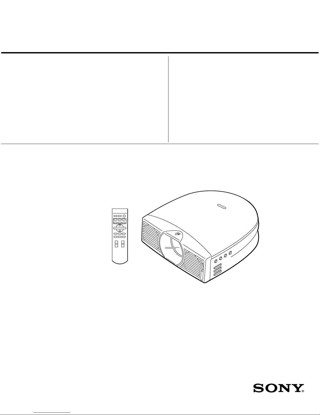
VIDEO PROJECTOR
VPL-HS10 Video Projector
VPLL-CT10/CW10 Projection Lens (Not Included)
RM-PJHS10 Remote Commander
REVISED-1

! WARNING
This manual is intended for qualified service personnel only.
To reduce the risk of electric shock, fire or injury, do not perform any servicing other than that
contained in the operating instructions unless you are qualified to do so. Refer all servicing to
qualified service personnel.
! WARNUNG
Die Anleitung ist nur für qualifiziertes Fachpersonal bestimmt.
Alle Wartungsarbeiten dürfen nur von qualifiziertem Fachpersonal ausgeführt werden. Um die
Gefahr eines elektrischen Schlages, Feuergefahr und Verletzungen zu vermeiden, sind bei
Wartungsarbeiten strikt die Angaben in der Anleitung zu befolgen. Andere als die angegeben
Wartungsarbeiten dürfen nur von Personen ausgeführt werden, die eine spezielle Befähigung
dazu besitzen.
! AVERTISSEMENT
Ce manual est destiné uniquement aux personnes compétentes en charge de l’entretien. Afin
de réduire les risques de décharge électrique, d’incendie ou de blessure n’effectuer que les
réparations indiquées dans le mode d’emploi à moins d’être qualifié pour en effectuer d’autres.
Pour toute réparation faire appel à une personne compétente uniquement.
WARNING!!
AN INSULATED TRANSFORMER SHOULD BE USED DURING
ANY SERVICE TO AVOID POSSIBLE SHOCK HAZARD, BECAUSE OF LIVE CHASSIS.
THE CHASSIS OF THIS RECEIVER IS DIRECTLY CONNECTED
TO THE AC POWER LINE.
SAFETY-RELATED COMPONENT WARNING !!
COMPONENTS IDENTIFIED BY A
!!
!!
! MARK ON THE SCHEMA TIC
DIAGRAMS, EXPLODED VIEWS AND IN THE PARTS LIST ARE
CRITICAL TO SAFE OPERATION. REPLACE THESE COMPONENTS WITH SONY PARTS WHOSE P ART NUMBERS APPEAR
AS SHOWN IN THIS MANUAL OR IN SUPPLEMENTS PUBLISHED BY SONY .
ATTENTION!!
AFIN D’ÉVITER TOUT RISQUE D’ÉLECTROCUTION
PROVENANT D’UN CHÂSSIS SOUS TENSION, UN
TRANSFORMA TEUR D’ISOLEMENT DOIT ETRE UTILISÉ LORS
DE TOUT DÉPANNAGE.
LE CHÂSSIS DE CE RÉCEPTEUR EST DIRECTEMENT
RACCORDÉ Á L’ALIMENTATION SECTEUR.
ATTENTION AUX COMPOSANTS RELATIFS Á LA
SÉCURITÉ!!
LES COMPOSANTS IDENTIFIÉS PAR UNE MAPQUE
!!
!!
! SUR
LES SCHÉMAS DE PRINCIPE, LES VUES EXPLOSÉES ET LES
LISTES DE PIECES SONT D’UNE IMPORTANCE CRITIQUE
POUR LA SÉCURITÉ DU FONCTIONNEMENT. NE LES
REMPLACER QUE PAR DES COMPOSANTS SONY DONT LE
NUMÉRO DE PIÈCE EST INDIQUÉ DANS LE PRÉSENT MANUEL
OU DANS DES SUPPLÉMENTS PUBLIÉS PAR SONY.
VPL-HS10

1 (P)
VPL-HS10
For the customers in the Netherlands
Voor de klanten in Nederland
Hoe u de batterijen moet verwijderen, leest u in de tekst
van deze handleiding.
Gooi de batterij niet weg maar lever deze in als klein
chemisch afval (KCA).
Für Kunden in Deutschland
Entsorgungshinweis: Bitte werfen Sie nur entladene
Batterien in die Sammelboxen beim Handel oder den
Kommunen. Entladen sind Batterien in der Regel dann,
wenn das Gerät abschaltet und signalisiert “Batterie
leer” oder nach längerer Gebrauchsdauer der Batterien
“nicht mehr einwandfrei funktioniert”. Um
sicherzugehen, kleben Sie die Batteriepole z.B. mit
einem Klebestreifen ab oder geben Sie die Batterien
einzeln in einen Plastikbeutel.


1
VPL-HS10
Table of Contents
1. Service Informations
1-1. Board Layouts .............................................................................................1-1
1-2. Disassembly ................................................................................................ 1-2
1-2-1. Front Panel Assy and Side Cover Assy Removal ......................1-2
1-2-2. HA, HB and NR Boards Removal .............................................1-3
1-2-3. HC, NF Boards and DC Fan Removal .......................................1-3
1-2-4. C Board Removal ....................................................................... 1-4
1-2-5. B Board Removal ....................................................................... 1-4
1-2-6. MS Board Removal....................................................................1-5
1-2-7. G Board and Lamp Power Supply Block Removal ...................1-6
1-2-8. MD, F Boards and Speaker Removal.........................................1-7
1-2-9. Optics Block Assy and U Board Removal ................................. 1-8
1-2-10. QA and QB Boards Removal .....................................................1-9
1-2-11. Extension Board and EXtension Connectors ...........................1-10
1-2-12. Extension Board and Extension Connectors Connection.........1-11
1-2-13. Connection Example ................................................................1-12
1-3. Service Knowhow .....................................................................................1-13
1-3-1. After Replacing the Prism Block .............................................1-13
1-3-2. After Replacing the Board .......................................................1-13
1-4. Memory ..................................................................................................... 1-14
1-5. Warning on Power Connection .................................................................1-16
2. Electrical Adjustments
2-1. Preparations.................................................................................................2-1
2-1-1. Equipment Required................................................................... 2-1
2-1-2. Factory Mode Setting ................................................................. 2-1
2-2. V COM Adjustment ....................................................................................2-1
2-3. Adjustment Item Initialize Data .................................................................. 2-3
2-4. White Balance Adjustment on Servicing ....................................................2-8
2-4-1. White Balance Adjustment ........................................................2-8
2-5. Tilt Adjustment ........................................................................................... 2-8
3. Semiconductors ..................................................................................3-1

2
VPL-HS10
4. Spare Parts
4-1. Notes on Repair Parts..................................................................................4-1
4-2. Exploded Views ..........................................................................................4-2
4-2-1. Cover ..........................................................................................4-2
4-2-2. Chassis........................................................................................ 4-4
4-2-3. Base ............................................................................................4-6
4-2-4. Optics .........................................................................................4-8
4-3. Electrical Parts List ...................................................................................4-10
4-4. Packing Materials & Supplied Accessories .............................................. 4-34
4-5. VPLL-CT10 .............................................................................................. 4-34
4-6. VPLL-CW10 ............................................................................................. 4-34
5. Block Diagrams
B, QA, QB and U Block ........................................................................... 5-1
C, HA, HB, HC, L, MD, NF and NR Block .............................................5-2
F and G Block ...........................................................................................5-4
MS Block ..................................................................................................5-5
6. Diagrams
6-1. Frame Schematic Diagram ..........................................................................6-2
6-2. Schematic Diagrams and Printed Wiring Boards........................................6-4
Schematic Diagrams
B ................................................................................................................6-5
C ..............................................................................................................6-15
F .............................................................................................................. 6-30
G.............................................................................................................. 6-31
HA...........................................................................................................6-34
HB ........................................................................................................... 6-35
HC ........................................................................................................... 6-36
L ..............................................................................................................6-37
MD ..........................................................................................................6-39
MS...........................................................................................................6-40
NF ...........................................................................................................6-44
NR ........................................................................................................... 6-44
QB ........................................................................................................... 6-46
QA...........................................................................................................6-49
U.............................................................................................................. 6-50

3
VPL-HS10
Printed Wiring Boards
B ..............................................................................................................6-14
C ..............................................................................................................6-26
F ..............................................................................................................6-30
G.............................................................................................................. 6-33
HA...........................................................................................................6-34
HB ........................................................................................................... 6-35
HC ........................................................................................................... 6-36
L ..............................................................................................................6-37
MD ..........................................................................................................6-38
MS...........................................................................................................6-43
NF ........................................................................................................... 6-44
NR ........................................................................................................... 6-44
QB ........................................................................................................... 6-45
QA...........................................................................................................6-48
U.............................................................................................................. 6-50

1-1
VPL-HS10
Section 1
Service Informations
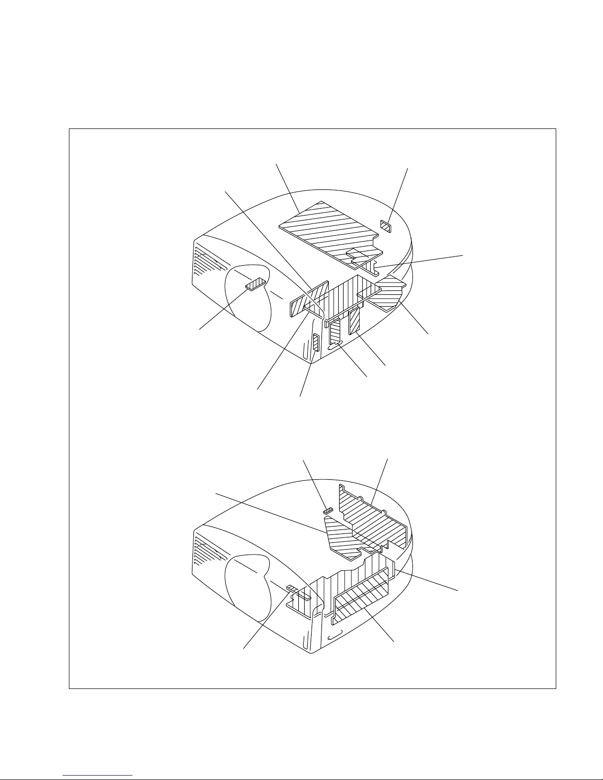
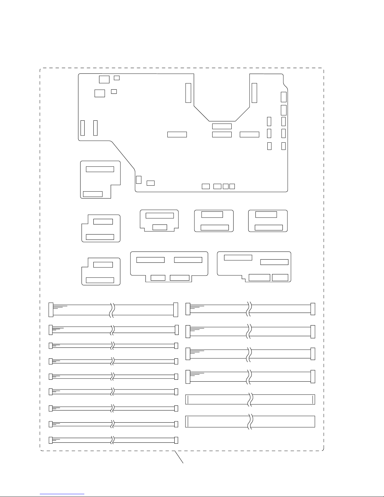
1-1. Board Layouts
C
MD
U
NR
QA
F
HB
HA
NF
Lamp power supply block
HC
B
L
QB
MS
G
1-2
VPL-HS10
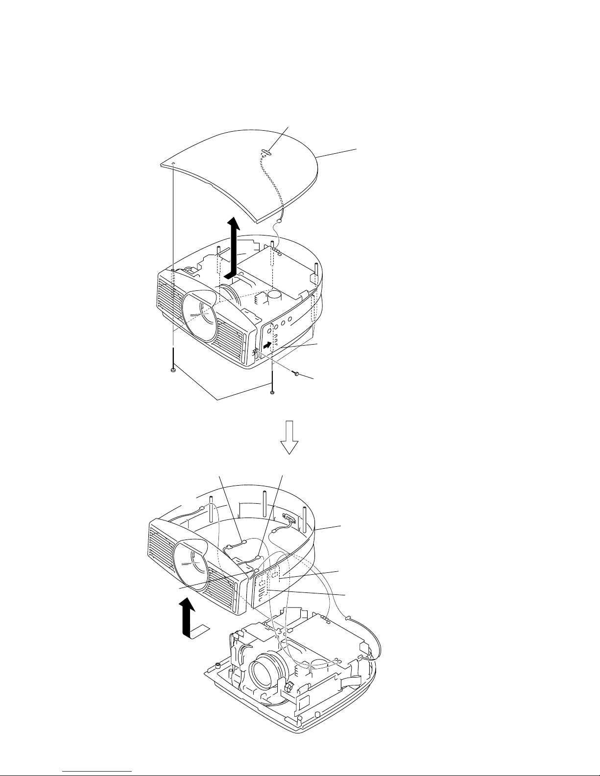
1-2. Disassembly
1-2-1. Front Panel Assy and Side Cover Assy Removal
3 Remove only one side of the side cover assy
in the direction of the arrow mark B.
(Do not give excessive force. Be careful not to break.)
C board
C board
1 Six shafts
A
C
CN604
CN62
CN603
HB board
HA board
B
L board
2 Remove the top cover assy
in the direction of the arrow A.
5 Remove the front panel assy, side cover assy
in the direction of the arrow C.
4 Screw
(+B 3x6)
CN610 (From DC fan)
CN63 (From HC board)
CN602 (From NF board)
CN611 (From DC fan)
1-3
VPL-HS10
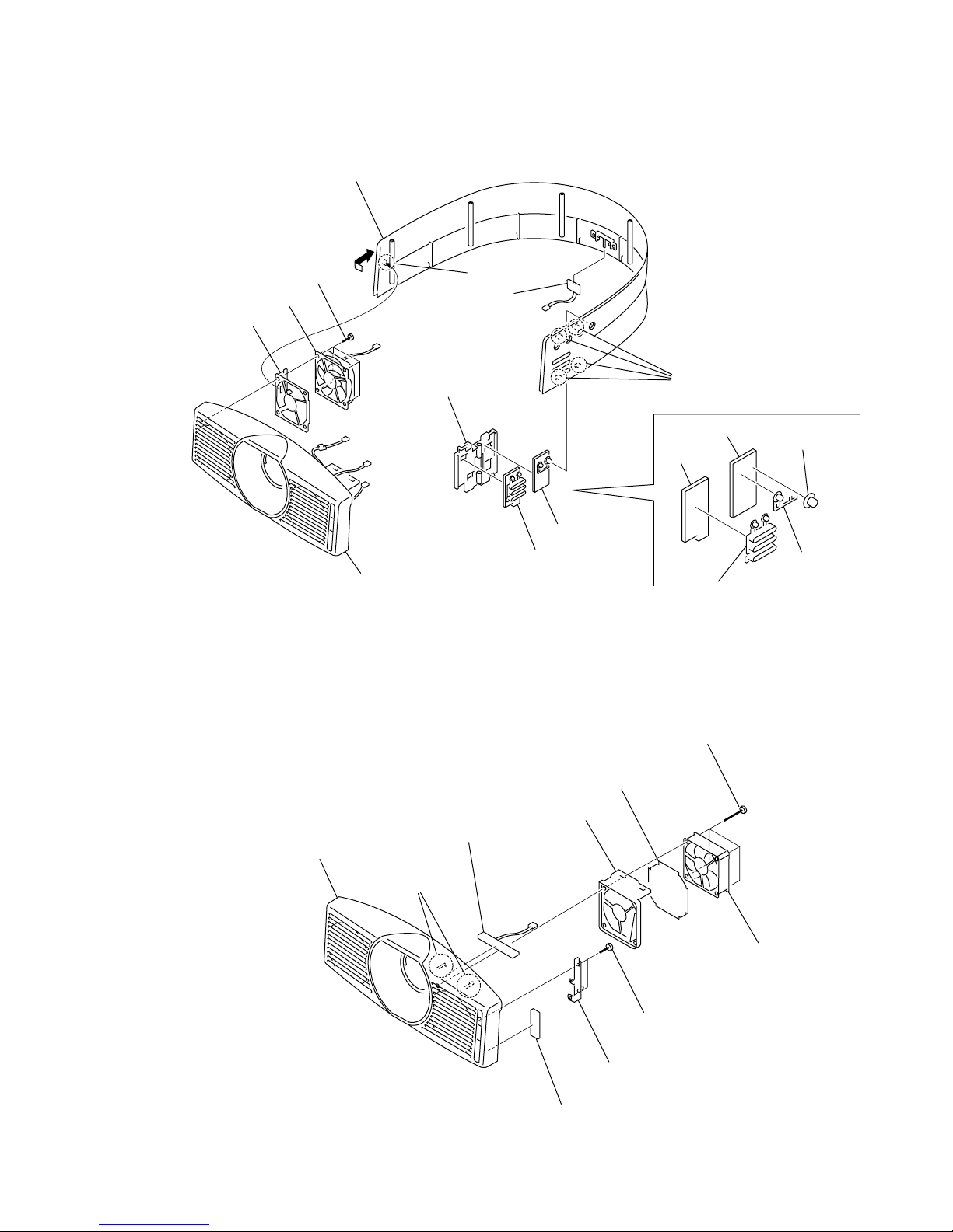
1-2-3. HC, NF Boards and DC Fan Removal
1-2-2. HA, HB and NR Boards Removal
Four claws
2 DC fan
3 Fan holder
7 H holder
9 HA board
5 Front panel assy
8 HB board
6 NR board
!/ HA button
!- HB1 button
!= HB2 button
Claw
HB board
HA board
4 Remove the side cover assy
in the direction of the arrow.
1 Four screws
(+PSW 3x10)
7 NF board
8 HC board
4 DC fan
2 Fan bracket
3 Guard
1
Four screws
(+PSW 3x30)
9 Front panel assy
5 T wo screws
(+B 3x6)
Two claws
6 FR holder
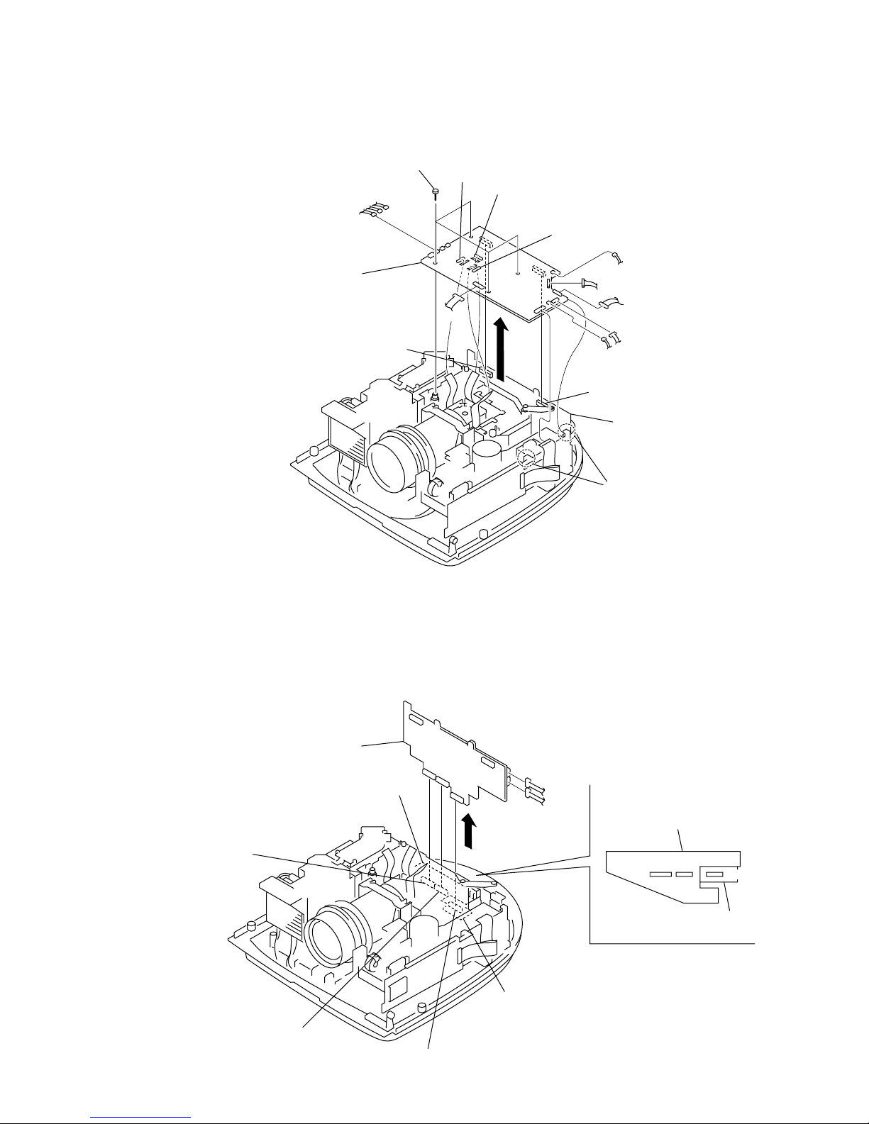
1-4
VPL-HS10
1-2-5. B Board Removal
To remove the B board, remove the C board beforehand.
CN600
CN860
CN820
CN770
CN201
CN304
CN601
CN607
CN606
CN609
CN608
CN612
CN605
CN112 (board to board)
CN111 (board to board)
B board
2 C board
1 Four screws
(+PSW 3 x12)
Two claws
CN103 (board to board)
CN102 (board to board)
CN902 (board to board)
B board
B board
QB board
QA board
QA board
CN105
CN106
CN103
CN102
CN902
1-2-4. C Board Removal
1-5
VPL-HS10
1-2-6. MS Board Removal
To remove the MS board, remove the C board beforehand.
2
screw
(+B 3x6)
4
MS board
1
Flat connector assy (50P)
3
Remove the MS bracket
in the direction of the arrow.
CN1001
Two claws
Four claws

1-6
VPL-HS10
1-2-7. G Board and Lamp Power Supply Block Removal
To remove the G board and lamp power supply block, remove the C board, MS board beforehand.
3
Two screws
(+B 3x6)
6
Two screws
(+B 3x6)
2
Power block assy
X3
CN600
CN702
CN703
4
Remove the G board
in the direction of the arrow.
7 Lamp
power supply block
Lamp power supply block
5 G
bracket cover
8
Power bracket
CN705
CN706
CN601
X1
1 Four screws
(+B 3x6)
Two claws

1-7
VPL-HS10
1-2-8. MD, F Boards and Speaker Removal
To remove the MD, F boards and speaker, remove the C board, MS bracket and power block assy beforehand.
2
MD board
1
MD bracket
CN802
CN801
CN502
5
Three screws
(+B 3x6)
3
Screw
(+B 3x6)
7
Three screws
(+B 3x6)
6
F board
8
Speaker spring assy
4
AC holder
9
Speaker
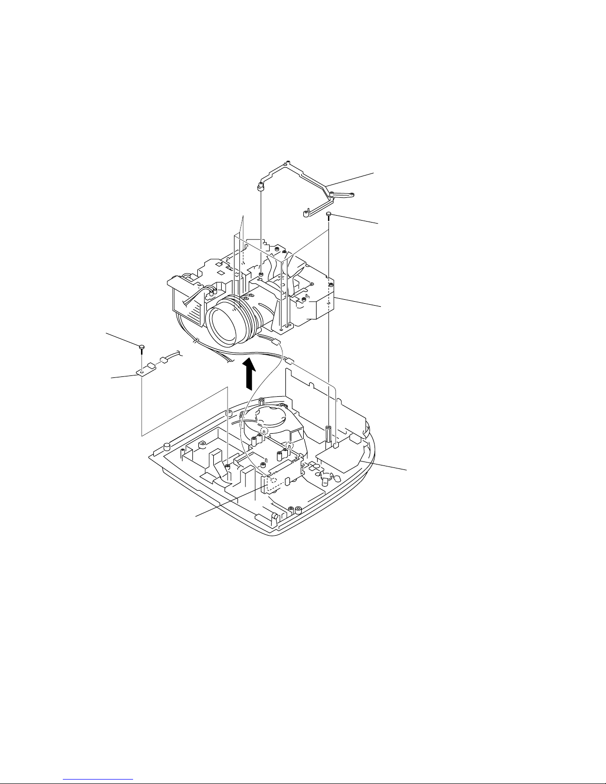
1-8
VPL-HS10
1-2-9. Optics Block Assy and U Board Removal
To remove the Optics block assy and U board, remove the C board, MS bracket and power block assy
beforehand.
2
Six screws
(+B 3x12)
1
C holder
CN802
CN502
3
Optics block assy
F board
MD board
CN41
4
Screw
(+B 3x6)
5
U board
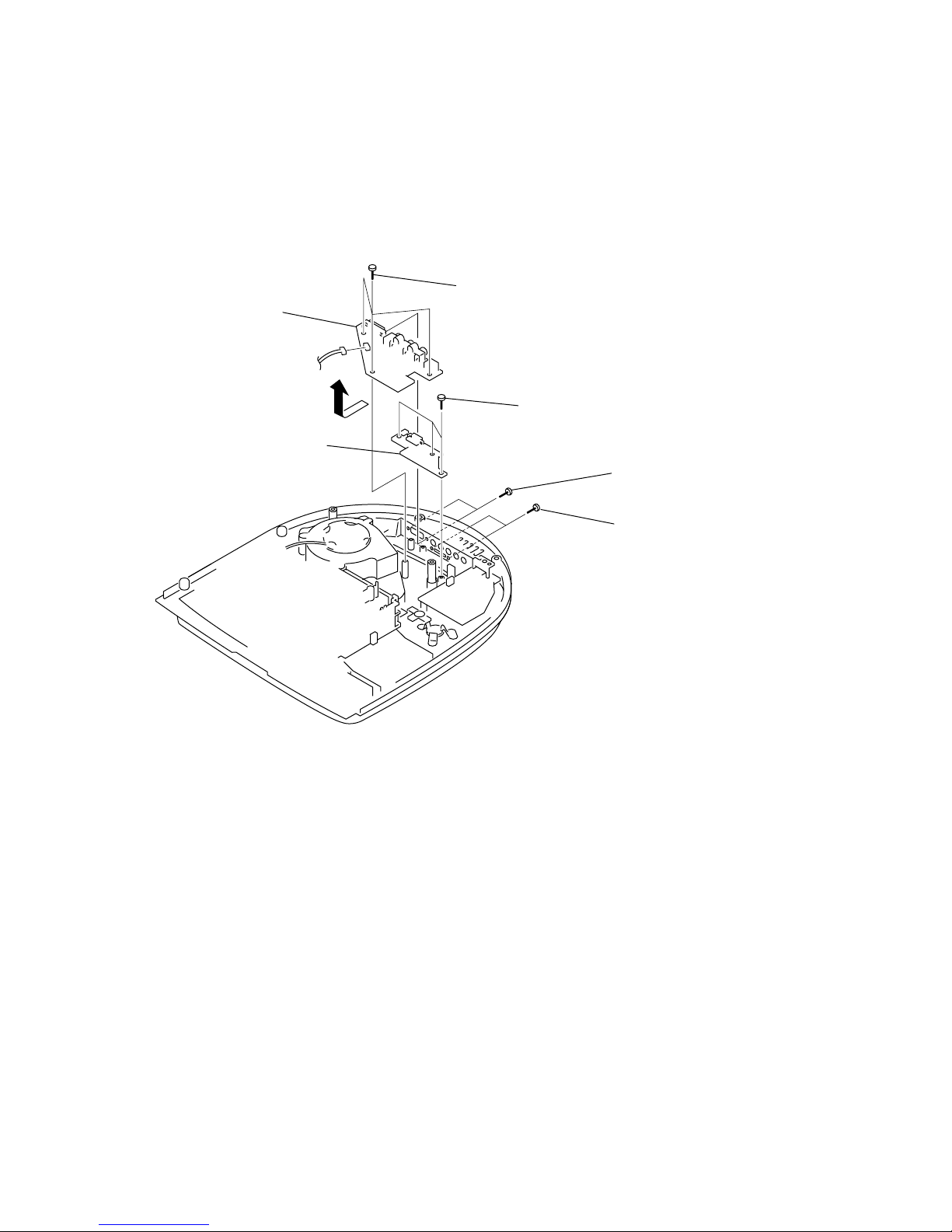
1-9
VPL-HS10
1-2-10. QA and QB Boards Removal
To remove the QA and QB boards, remove the C board, MS bracket, power block assy and Optics block
assy beforehand.
4
Three screws
(+B 3x6)
5
Two screws
(+M 1.6x5)
2
Two screws
1
Three screws
(+B 3x6)
6 QA board
3 QB board
CN101
1-10
VPL-HS10
1-2-11. Extension Board and EXtension Connectors
X1 board
X4 board
X3 board
X5 board
X7 board X6 board
X2 board X2 board
X3 board
SR connector assy (12P)
ZH connector assy (7P)
ZH connector assy (8P)
ZH connector assy (10P)
ZH connector assy (9P)
Three flat connectors assy (32P)
SR connector assy (5P)
SR connector assy (3P)
Two PH connectors assy (3P)
ZH connector assy A (3P)
ZH connector assy B (3P)
SR connector assy (2P)
ZH connector assy (4P)
SR connector assy (4P)
X kit assy (A-1604-096-A)
Eight flat connectors assy (50P)
1-11
VPL-HS10
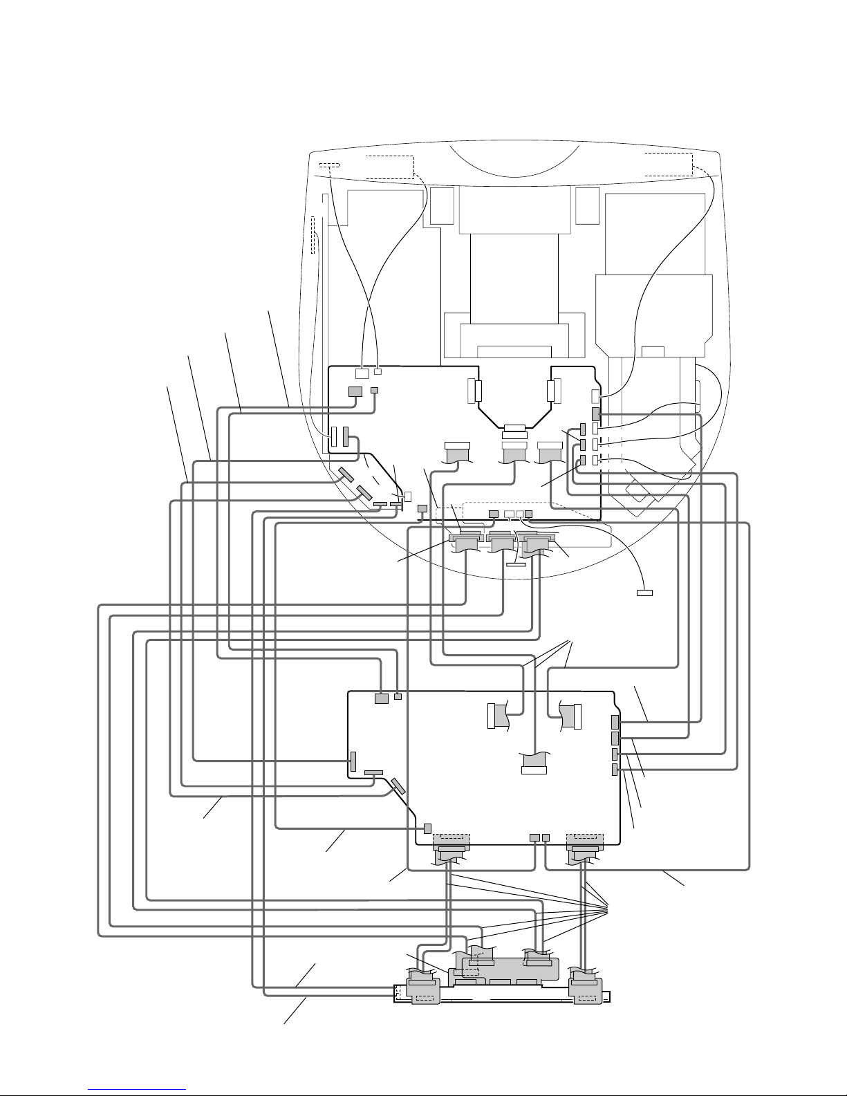
1-2-12. Extension Board and Extension Connectors Connection
X1
G
C
B
X4
X6
QB
QA
NF
NR
L
DC fan
DC fan
X3
X3
X2X2
X7
X5
CN610
CN610
CN110
CN601
CN601
CN101
CN705
CN607
CN771
CN606
CN606
CN501
CN502
CN23
CN22
CN23
CN22
CN33
CN33
CN32
CN32
CN108CN107 CN110
CN112
CN72
CN73
CN75
CN52
CN111
CN106
CN105
CN106
CN861
CN820
CN820
CN770
CN770
CN860
CN860
CN111
CN112
CN103 CN104
CN604
CN103
CN102
CN902
CN603
CN604
CN603
CN611
CN611
CN609
CN608
CN612
CN109
CN108
CN821
CN706
CN702
CN703
CN605
CN102
CN602
CN602
SR connector assy
(12P)
SR connector assy (3P)
SR connector assy (5P)
SR connector assy (2P)
Flat connector assy
(32P)
Flat connector assy
(50P)
CN609
CN608
CN612
PH connector assy (3P)
PH connector assy (3P)
ZH connector assy
(7P)
ZH connector assy (8P)
ZH connector assy A
(3P)
ZH connector assy (4P)
ZH connector assy B (3P)
ZH connector ass
y (9P)
ZH connector assy
(10P)
SSR connector assy (4P)
HB
1-12
VPL-HS10
1-2-13. Connection Example
For C Board
Flat connector assy (32P)
Flat connector assy (50P)
Flat connector assy (50P)
Flat connector assy (50P)
Flat connector assy (50P)
Flat connector assy (32P)
Flat connector assy (50P)
X1
X6
X4
C
C
X7
X3
X3
X2
X2
B
B
QA
QB
QB
X7
X7
X6
X4
QA
X1
X6
X4
C
X5
X3
X2
X2
X3
B
QA
QB
X5
X5
For C and B Boards
For B Board
1-13
VPL-HS10
1-3. Service Knowhow
1-3-1. After Replacing the Prism Block
1. Perform Section “2-2. V COM Adjustment.”
2. Perform the Gamma data writing of the Prism Block.
3. Perform Section “2-4. White Balance Adjustment on
Servicing.”
1-3-2. After Replacing the Board
. Refer to the cross table shown on right.
. There are no need to perform the adjustment when the board
other than the B board or C board had been replaced.
1) When Replacing the B Board
When the data before replacement can be read properly
1. Make a note of the data before replacement. After
replacement, write the data into the new board with
service mode.
2. If the white balance is extremely deteriorated, perform
the white balance adjustment (Refer to Section 2-4.).
When the data before replacement cannot be read
1. Perform Section “2-2. V COM Adjustment.”
2. Perform Section “2-4. White Balance Adjustment on
Servicing.”
3. Perform Section “2-5. Tilt Adjustment.”
2) When Replacing the C Board
1. Before replacement, unsolder the IC705 from the
replaced C board and then mount it to the new board.
2. Perform Section “2-2. V COM Adjustment.”
3. If the white balance is extremely deteriorated, perform
the white balance adjustment (Refer to Section 2-4.).
4. Perform Section “2-5. Tilt Adjustment.”
3) When Replacing the Other Board
There are no need to perform the adjustment.
Cross Table of Board Replacement
Board Name
Device Name Item Name B C
OTHER TILT C0 * O
TILT C1 * O
TILT C2 * O
P.DRV VCOM (R) * O
VCOM (G) * O
VCOM (B) * O
W/B ADJUST
INPUT-A HIGH GAIN R * O
GAIN G * O
GAIN B * O
BIAS R * O
BIAS G * O
BIAS B * O
INPUT-A LOW GAIN R * O
GAIN G * O
GAIN B * O
BIAS R * O
BIAS G * O
BIAS B * O
INPUT-A HIGH GAIN R * O
GAIN G * O
GAIN B * O
BIAS R * O
BIAS G * O
BIAS B * O
INPUT-A MID GAIN R * O
GAIN G * O
GAIN B * O
BIAS R * O
BIAS G * O
BIAS B * O
VIDEO MID GAIN R * O
GAIN G * O
GAIN B * O
BIAS R * O
BIAS G * O
BIAS B * O
VIDEO LOW GAIN R * O
GAIN G * O
GAIN B * O
BIAS R * O
BIAS G * O
BIAS B * O
* : When down the data before replacement, and then
write in the data after the board replacement.
O : Need adjustment
Value: See description.
1-14
VPL-HS10
Gamma memory is actualized through Gamma mode
functions’offsetting the output values to the Contrast and
Brightness devices.
When the power plug is connected to the power line
(Standby status), all data inside the internal ROM are
written into the NVM (Nonvolatile Memory). When the
power is turned to on, required data for the current picture,
such as status memory data, etc., are selected, and they are
written into the internal RAM.
When adjustment is carried out, adjustment data are
written into the NVM automatically (items on the user
mode) or by the trigger of memory operation (items on the
service mode and special service mode), then stored them.
Adjustable items (W/B and Device Adjust) of the service
mode and special service mode are memorized into the
NVM by the memory operation. At the same time, the
factory preset (adjusted) data are all eliminated from the
memory.
1-4. Memory
Memory structure consists of the following five memory
blocks.
1. Set memory
2. Status memory
3. Chroma memory
4. W/B memory
5. Channel memory
6. Image Flip memory
7. Picture memory
CPU internal ROM : 384 kbyte Flash Memory
CPU internal ROM : 16 kbyte
External NVM memory : 8 kbyte EEPROM
NT358/443/BW60
PAL/PAL-M/N/
SECAM/BW50
15k RGB
Component (15k)
Two times speed
Component
HDTV (YPbPr)
NT358/443/BW60
PAL/PAL-M/N/
SECAM/BW50
15k RGB
Component (15k)
Two times speed
Component
HDTV (YPbPr)
HDTV (GBR)
(Include two times speed)
HDTV (GBR)
(Include two times speed)
HIGH
LOW
Computer
MIDDLE
HIGH
LOW
MIDDLE
Others
HIGH
LOW
Computer
MIDDLE
HIGH
LOW
MIDDLE
Others
W/B
Memory
HIGH
LOW
MIDDLE
No.02
No.03
No.04
...
No.99
No.01
Status
Memory
No.01
No.02
No.03
No.04
...
No.99
Status
Memory
Set Memory Set Memory Set Memory
Status Memory
Chroma Memory
Input-A
Preset
No.03
No.04
...
No.99
Component
No.101
...
No.120
Input-A
User
No.03
No.04
...
No.99
Digital
Preset
No.121
...
No.140
Digital
User
No.53
No.69
...
MS
Chroma
Memory
Chroma
Memory
W/B
Memory
W/B
Memory
1-15
VPL-HS10
Turn over to the upper and
lower sides
No turn over to the upper
and lower sides
Turn over to the upper and
lower sides
No turn over to the upper
and lower sides
CPU ROM
External NVM
CPU RAM
Initialize
Active memory copy
Memory
Channel Memory
Image Flip Memory
Channel
Memory
Video 1
S Video 1
Input-A
Video 2
S Video 2
Component
Digital
MS
Channel
Memory
Video
S Video
Input-A
Video 2
S Video 2
Component
Digital
MS
Picture Memory
Dynamic
Standard
Cinema
User1
User2
User3
Picture
Memory
Picture
Memory
Video 1
Video 1
Dynamic
Standard
Cinema
User1
User2
User3
Dynamic
Standard
Cinema
User1
User2
User3
S Video 1
S Video 1
Dynamic
Dynamic
Standard
Cinema
User1
User2
User3
Dynamic
Standard
Cinema
User1
User2
User3
Video 2
Video 2
Dynamic
Standard
Cinema
User1
User2
User3
Dynamic
Standard
Cinema
User1
User2
User3
S Video 2
S Video 2
Dynamic
Standard
Cinema
User1
User2
User3
Dynamic
Standard
Cinema
User1
User2
User3
Input-A
Input-A
Standard
Cinema
User1
User2
User3
Dynamic
Standard
Cinema
User1
User2
User3
Component
Component
Dynamic
Standard
Cinema
User1
User2
User3
Dynamic
Standard
Cinema
User1
User2
User3
Digital
Digital
Dynamic
Standard
Cinema
User1
User2
User3
Dynamic
Standard
Cinema
User1
User2
User3
MS
MS
Dynamic
Standard
Cinema
User1
User2
User3
Image Flip
Memory
Image Flip
Memory

1-16
VPL-HS10
1-5. Warning on Power Connection
Use a propre power cord for your local power supply.
The United States, Continental UK Australia Japan
Canada Europe
Plug type YP-11 YP-21 SP-61 B8 YP-13
Female end YC-13L YC-13L YC-13L C7-2 YC-13L
Cord type SPT-2 H03VVH2-F H03VVH2-F H03VVH2-F VCTFK
Rated Voltage & Current 10 A/125 V 2.5 A/250 V 2.5 A/250 V 2.5 A/250 V 7 A/250 V
Safety approval UL/CSA VDE BS SAA DENANHO
Cord length (max.) 4.5 m – – – –

2-1
VPL-HS10
Section 2
Electrical Adjustments
2-1. Preparations
2-1-1. Equipment Required
. Oscilloscope
Tektronix 2465 or equivalent
(bandwidth: 350 MHz or more)
. NTSC, PAL, SECAM component signal generator
T ektronix TG2000 + AVG1 (optional module) + AWVG1
(optional module) or equivalent
. VG (Programmable video signal generator)
VG814 or equivalent
. Digital voltmeter
Advantest TR6845 or equivalent
. Luminance meter
. Chrominance difference gauge
n
Perform the following adjustments at least 5 minutes after
turning on the power.
2-1-2. Factory Mode Setting
1. Make sure that the MENU is indicated.
2. Exit the menu.
3. Press the keys in the following order:
“ENTER” → “ENTER” → “LEFT” → “ENTER”
4. The message “Do you wish to enter into the
FACTORY MODE? Yes:↑ No:↓ ” will be displayed.
5. Select “Yes:↑”.
n
. When leaving the FACTORY MODE, perform item 3.
“Do you wish to return to the USER MODE? Yes:↑ No:↓
” will be displayed. Select “Yes:↑”.
. Cannot enter FACTORY MODE by MS channel.
2-2. V COM Adjustment
1. Input the green-only XGA 1 Lime ON/OFF signal to
INPUT-A, and set the CONTRAST to 70.
2. Set the screen to G VCOM adjustment of “Device
Adjust.”
3. Adjust the G VCOM so that the flicker on the screen is
minimum.
4. Change the input signal to the red-only and blue-only
1 line ON/OFF signal respectively and adjust R
VCOM and B VCOM respectively so that the flicker
becomes minimum as described in step 3.
5. Save the value adjusted.
6. Set the “Image Flip” to either “V” or “HV”.
7. Input the R/G/B value adjusted as above step 5.
8. Save the value adjusted.
9. Set the “Image Flip” to “OFF”.
2-2
VPL-HS10
2-3. Adjustment Item Initialize Data
* : “Dot Phase, H Size, Shift H/V and Picture Mode” in the “INPUT SETTING” menu have an initial value
respectively in accordance with the input signal (PRESET MEMORY No.).
Note : There are nonadjustable items in accordance with the input signal.
MenuTitle ItemName
Set Memory Status Memory
Video 1/S Video1/Video 2/S Video 2
Dynamic Standard Cinema User1/2/3
Dynamic
90
50
60
50
50
–
–
Low
Middle
Film
Off
Full
4
4
0
80
50
50
50
50
–
–
Low
High
Film
On
80
50
50
50
50
–
–
Off
Low
Film
On
80
50
50
50
50
–
–
Off
Low
Film
On
90
50
60
50
50
20
Low
Graphics
Middle
20
Graphics
High
20
Graphics
Low
20
Graphics
Low
Film
Off
80
50
50
50
50
Low
Film
On
80
50
50
50
50
Off
Film
On
80
50
50
50
50
Off
Film
On
Full
4
4
0
Full
4
4
0
Full
4
4
0
Full
4
4
0
Full
4
4
0
Full
4
4
0
Full
4
4
0
30
On
On
Component
Video GBR
Auto
Off
On
On
English
Center
Black
Auto
0
0
Off
Blue
On
Indication only
Indication only
Indication only
Indication only
Indication only
Indication only
Indication only
Indication only
Indication only
15 (*)
*
*
PICTURE SETTING Picture Mode
Adjust Picture...
Volume
Adjust Signal...
V Position (Sub Title)
Title Area
Smart APA
Auto Input Search
Input-A Signal Sel.
Digital Signal Sel.
Color System
Power Saving
Illumination
Status
Languege
Menu Position
Menu Color
V Keystone
Side Shot
Image Flip
Background
Test Pattern
fH
fV
(Memory No.)
(Resolution)
Lamp Timer
ROM Version
SC ROM Version
Operation Timer
Prev. Lamp Timer
Gain R
G
B
Bias R
G
B
V Position (Zoom)
Wide Mode
INPUT SETTING
SET SETTING
MENU SETTING
Contrast
Brightness
Color
Hue
Sharpness
RGB Enhancer
Black Level Adj.
Gamma Mode
Color T emp.
DDE
Cinema Black
Dot Phase
H Size
Shift
Manual...
INSTALL SETTING
INFORMATION
W/B SETTING
Input-A/Digital
Picture Memory
Memory Name
Dynamic Standard Cinema User1/2/3

2-3
VPL-HS10
90
50
60
50
50
–
–
Low
Middle
Off
80
50
50
50
50
–
–
Off
Low
Film
On
80
50
50
50
50
–
–
Off
Low
Film
On
80
50
50
50
50
–
–
Off
Low
Film
On
90
50
60
–
–
20
Middle
Off
80
50
50
–
–
20
High
On
80
50
50
–
–
20
Low
On
80
50
50
–
––––
––––
–
20
Low
On
182
182
182
85
85
85
150
182
160
85
85
85
150
182
160
85
85
85
160
160
160
85
85
85
140
160
150
85
85
85
140
160
150
85
85
85
Graphics Graphics Graphics Graphics
Film
Full
4
4
0
Full
4
4
0
Full
4
4
0
Full
4
4
0
–
–
–
–
–
–
–
–
–
–
–
–
–
–
–
–
Remarks
Picture Memory
Memory Name
Component
Dynamic Standard Cinema User1/2/3MSDynamic Standard Cinema User1/2/3
Video
W/B Memory
High Middle Low
Computer
High Middle Low
2-4
VPL-HS10
Note : There are nonadjustable items in accordance with the input signal.
*1 : Depends on the color system and the input terminal.
*2 : Depend on the input signal.
DeviceName ItemName
Set Memory Status Memory Chroma Memory
NT358/NT443
/BW60
Pal/Pal-M/N/
Secam/BW50
15kRGB
Component
(15k)
*2
*2
32
*1
–
Indication only
Indication only
Adjustment is
impossible
143
40
196
161
161
161
1
10
0
0
0
31
31
31
0
1
25
32
2
8
125
64
128
64
64
124
73
128
64
64
128
64
119
67
64
128
64
119
67
64
–
–
–
–
–
–
–
–
–
–
–
–
–
–
–
A/D Converter ADC/ Clamp Position
Clamp Width
R Gain (Other)
R Gain (Component)
R Gain (VideoGBR)
G Gain (Other)
G Gain (Component)
G Gain (VideoGBR)
B Gain (Other)
B Gain (Component)
B Gain (VideoGBR)
R Offset (Other)
R Offset (Component)
R Offset (VideoGBR)
G Offset (Other)
G Offset (Component)
G Offset (VideoGBR)
B Offset (Other)
B Offset (Component)
B Offset (VideoGBR)
Post Coast
Pre Coast
Sync Sep Th
Ch1 Gain
Ch2 Gain
Video Brt
Video Cont
Sub Color
LCBW
Y-DeLay
Ch3 Gain
Ch4 Gain
YUV Brt
YUV Cont
1E
AOSL
1F
Offset R
Offset G
Offset B
V Common R
V Common G
V Common B
Psig 1
Psig 2
Signal Center
Gain R
Gain G
Gain B
DCFB Off
SH1
V Com Pth Enb
Installation
Sub Cont
Sub Brt
R Osd Lvl
G Osd Lvl
B Osd Lvl
Through
SW
APC Thres
APC Limit
3D GammaOther
Other/
Chroma/D.Comb
Chroma/
Panel Driver P.Drv
Sample Hold/
Memory Name
Two times speed
Component
HDTV
(YPbPr)
HDTV(GBR)
Include two times speed
2-5
VPL-HS10
–
–
–
–
–
–
–
–
–
–
–
–
–
–
–
–
–
–
–
–
–
–
–
–
–
–
–
–
–
–
–
–
–
–
–
–
16
60
144
144
0
16
60
144
144
0
160
144
160
160
0
260
144
260
260
211
211
83
83
83
211
211
211
83
83
83
211
0
16
60
144
144
0
16
60
144
144
0
–
–
–
–
–
–
–
–
–
–
–
–
–
–
–
–
–
–
–
–
–
–
–
–
–
–
–
–
–
–
–
–
–
–
–
–
–
–
–
–
–
–
–
–
–
–
–
–
–
–
–
–
–
–
–
–
–
–
–
–
–
–
–
–
–
–
–
–
–
–
–
–
–
–
–
–
–
–
–
–
–
–
–
–
–
–
–
–
–
–
–
–
––
–
–
–
–
100
100
100
100
100
100
100
100
100
128
100
128
128
128
128
128
100
100
100
100
100
128
100
128
Remarks
Channel Memory
Memory Name
Video 1 S Video 1 Input-A Video 2 S Video 2 Component Digital MS
Image Flip Memory
Turn over to the upper
and lower sides
No turn over to the
upper and lower sides
2-6
VPL-HS10
Note : There are nonadjustable items in accordance with the input signal.
DeviceName ItemName
Set Memory Status Memory Chroma Memory
NT358/NT443
/BW60
Pal/Pal-M/N/
Secam/BW50
15kRGB
Component
(15k)
6
0
216
40
3
4
1
0
3
1
128
0
V StartOther/Other
H Start (MSB)
H Start (LSB)
H Position
HST Position
HST Phase
Temp Lamp
Temp Panel
Fan1 H
Fan1 L
Fan2 H
Fan3 L
Fan3 H
Fan2 L
Synchronous
Tilt C0
Tilt C1
Tilt C2
X Tilt
Y Tilt
TL
TP
Highland Mode
Gamma
CTI T apIp/IP
CTI Limit
CTI Shift
CTI Gain
Sharp Limit
MD Thresh C
MD Thresh O
VS
Continue
Edit Detect
Indicator
Manual
Manual Pair
Manual State
Field Times
Noise Thresh
Disp Area
PULL Area T
PULL Area B
PULL Area L
PULL Area R
VS Limit
Edge Det Less
VS Core
X Only
Hysteresis
Hysteresis Data
Thresh Still Large
Thresh Still Med
Thresh Still Small
22 Pre Post Rate
22 Pre Post Thresh
Film Times 22
Sudare Rate 32Ip2/
Sudare Thresh 32
Sudare Rate 22
Sudare Thresh 22
255
8
16
1
1
0
0
0
0
0
2
4
0
71
203
165
765
64
1
4
0
1
2
2
3
4
15
2
3
4
64
4
40
Memory Name
HDTV
(YPbPr)
Adjustment is
impossible
Adjustment is
impossible
Indication only
Factory default
setting value
Factory default
setting value
Factory default
setting value
Factory default
setting value
Indication only
Indication only
Indication only
Two times speed
Component
HDTV(GBR)
Include two times speed
 Loading...