

Page 1
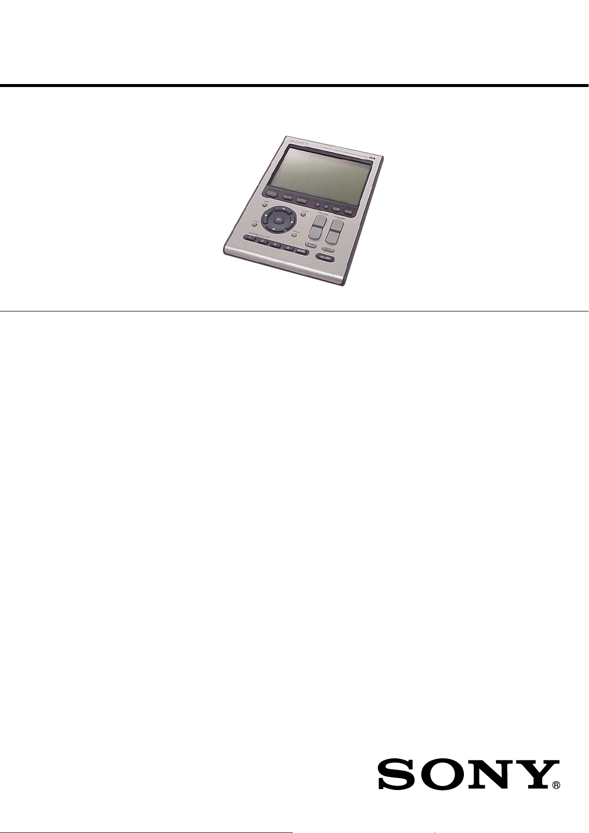
RM-AX4000
SERVICE MANUAL
Ver. 1.0 2005.08
SPECIFICATIONS
Operating distance
Approx. 32.8 ft. (10 meters) (varies depending
on components of different manufacturers)
Power requirements
Remote control and backlight: Four size AA
(R6) batteries
Battery life
Approx. 5 months (a Sony TV turned on/off
up to approx. 300 times per day)
Dimensions
Approx. 4 3/4 1 1/4 7 in. (w h d)
(118 31.2 175 mm)
Mass
12 oz. (320 g) (not including batteries)
Learnable signals*
Capacity per signal: up to 300 bit
Signal frequency range: 455 kHz and up to
300 kHz
Signal interval: up to 1 second
× × × ×
× ×
Supplied accessories
•
•
•
•
•
* Some signals cannot be learned by the
Design and specifications are subject to change
without notice.
US Model
USB mini cable (1)
CD-ROM for the AX Remote Editor software,
PDF file Operating Instructions (1)
Quick Start Guide (1)
Preset code lists (1)
Warranty Card (1)
Remote Commander, even though the signals
comply with these specifications.
9-879-792-01
2005H1678-1
© 2005.08
INTEGRATED REMOTE COMMANDER
Sony Corporation
Personal Audio Group
Published by Sony Engineering Corporation
Page 2

RM-AX4000
TABLE OF CONTENTS
1. GENERAL ................................................................... 3
2. DISASSEMBLY
2-1. CASE (Lower)................................................................. 7
2-2. KEY Board and LCD Section ......................................... 7
2-3. MAIN Board and LCD Module ...................................... 8
3. TEST MODE ............................................................... 9
4. DIAGRAMS
4-1. Block Diagram – MAIN Section –.................................. 12
4-2. Printed Wiring Board – MAIN Board – .......................... 13
4-3. Schematic Diagram – MAIN Board – ............................. 14
5. EXPLODED VIEWS ................................................. 17
6. ELECTRICAL PARTS LIST .................................. 18
Flexible Circuit Board Repairing
• Keep the temperature of the soldering iron around 270 °C
during repairing.
• Do not touch the soldering iron on the same conductor of the
circuit board (within 3 times).
• Be careful not to apply force on the conductor when soldering
or unsoldering.
Notes on chip component replacement
• Never reuse a disconnected chip component.
• Notice that the minus side of a tantalum capacitor may be
damaged by heat.
UNLEADED SOLDER
Boards requiring use of unleaded solder are printed with the leadfree mark (LF) indicating the solder contains no lead.
(Caution: Some printed circuit boards may not come printed with
the lead free mark due to their particular size)
: LEAD FREE MARK
Unleaded solder has the following characteristics.
• Unleaded solder melts at a temperature about 40 °C higher
than ordinary solder.
Ordinary soldering irons can be used but the iron tip has to be
applied to the solder joint for a slightly longer time.
Soldering irons using a temperature regulator should be set to
about 350 °C.
Caution: The printed pattern (copper foil) may peel away if
the heated tip is applied for too long, so be careful!
• Strong viscosity
Unleaded solder is more viscou-s (sticky, less prone to flow)
than ordinary solder so use caution not to let solder bridges
occur such as on IC pins, etc.
• Usable with ordinary solder
It is best to use only unleaded solder but unleaded solder may
also be added to ordinary solder. Operating instructiondd
2
Page 3
SECTION 1
GENERAL
RM-AX4000
This section is extracted
from instruction manual.
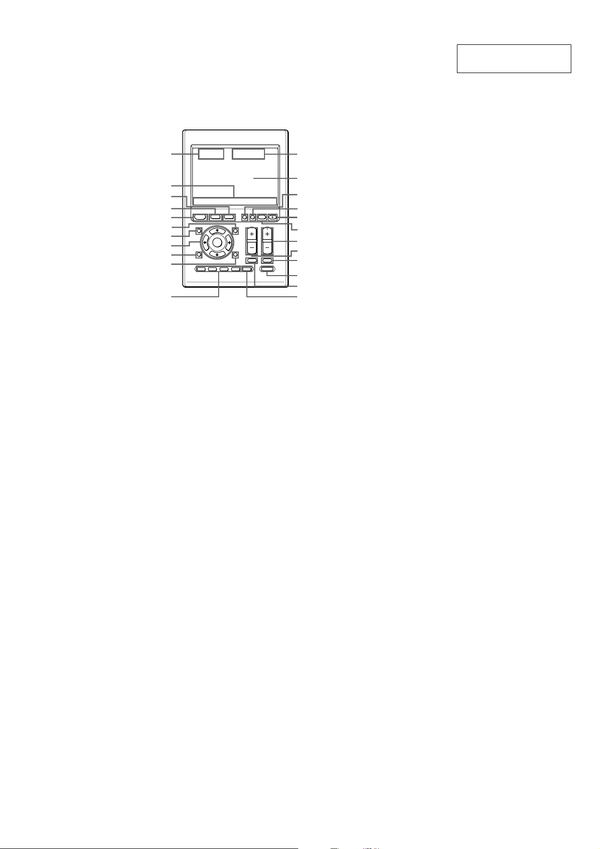
Location and function
of controls
1
2
3
4
5
6
7
8
9
0
X
PRESS
COMPONENT
BACK
EPG
OK
EXIT TOOLS
SYSTEM CONTROL
1 MORE43
2
MENU
qa
The CHANNEL + button has a tactile dot.
1 Clock display (pages 11, 42)
Displays the clock, the transmission
mark, the battery mark and the timer
mark.
2 Label keys
Different keys appear depending on
the selected display. The Label keys
are used mainly to choose the XPRESS
function/component/System
Control/Timer/setting items, etc. You
can change the names of the XPRESS
function, components, System Control
key and Timer as the Label keys.
3 COMPONENT button (page 27)
The component names appear as the
Label keys. When you press a
component name, the operating
display for that component appears.
4 BACK button (page 24)
Used to return to the previous display.
5 XPRESS button (pages 22-24)
The XPRESS names appear as the
Label keys. When you press an
XPRESS name, the operating display
for that XPRESS function appears, and
its macro is performed.
6 MENU button
(pages 76-87)
Calls up the menu screen for
components that have menu function.
7 EPG button
(pages 76, 78, 81, 84, 86)
8 OK and Cursor Control buttons
(pages 40, 46, 62, 67, 76, 78-81,
83-88)
9 EXIT button
(pages 39, 76, 78-81, 83-87)
q; TOOLS button
(pages 76, 78, 81, 84, 86)
qa SYSTEM CONTROL buttons
(pages 31, 51, 54)
You can automatically carry out the
entire program by pressing one
button.
SYNC-UP
VOLUME
MUTING
CHANNEL
RECALL
ALL OFF
COMMANDER
OFFLIGHTTIMER
qs
qd
qf
qg
qh
qj
qk
ql
w;
wa
ws
wd
qs Display title
Shows the title of the LCD Display. If
a page number such as “/1” appears,
multiple pages are available. If you
press the number, next page displays.
qd Touch-keys
The keys are used for setting the
Remote Commander and operating
each component appear on the LCD
display.
Note
Do not press the touch-keys using sharp
objects such as pins or ball-point pens.
qf SYNC-UP button
(pages 25, 49, 55)
Used to synchronize with the status of
a component .
qg TIMER button (pages 29, 30)
Used to set the timer program on/off.
qh COMMANDER OFF button (page 33)
Turns the power of the Remote
Commander off.
qj LIGHT button (pages 32, 49)
Used to brighten the backlight in the
dark. Press the button once to turn
on/off the light.
qk CHANNEL +/– buttons
(pages 76-78, 80-81, 83-87)
Selects the channel.
ql VOLUME +/– buttons*
(pages 29, 50, 76-90)
Adjusts the volume.
w; RECALL button
(pages 76-78, 81, 84-86, 91)
wa ALL OFF button (page 33)
ws MUTING button*
(pages 29, 50, 76-90)
Silences the sound. Press the button to
silence, and again to return to the
previous volume level.
wd MORE button (pages 31, 51, 55)
The System Control keys (SYSTEM5-
8) are displayed as the Label keys.
When you press a System Control key,
its macro is performed.
Note
No default System Control key macros are
set at the factory.
* Note on the VOLUME +/– and
MUTING buttons
The Remote Commander can control or
silence the TV and amplifier's volume when
you select a visual or audio component.
Note on the LCD display’s power
on/off
To turn on the LCD display, press any button
except the COMMANDER OFF button.
To turn off the LCD display, press the
COMMANDER OFF button. If you do not use
the Remote Commander within 5 minutes, the
LCD display automatically turns off.
This interval can also be changed (page 37).
3
Page 4

RM-AX4000
Setting the clock
When you install batteries the first time,
the Remote Commander enters clock
setup mode.
“DS_TIME” appears as the Display title.
“STD_TIME” lights and “SET” and
“DS_TIME” flash on the Label keys.
STD_TIME: standard time
DS_TIME: daylight savings time
SU
LEARN
NG
DS_TIME
SET [STD_TIME] DS_TIME
1
Press “STD_TIME” or
“DS_TIME” on the Label keys.
or
The current setting is shown inside
the [ ], while the other flashes.
If the summer time (daylight savings
time) is used in your area, press the
DS_TIME key. When the time change
occurs (in spring and autumn), the
Remote Commander will
automatically adjust itself.
If the summer time is not used in your
area, press the STD_TIME key.
2
Press “SET” on the Label keys.
SET
Next, press the g button. The day of
the week is set.
“12” (hour) “AM” and “SET” flash.
SU
LEARN
NG
AM
CLOCK
SET STD_TIME
Note
If you press the G button, the day of the
week is set and setting mode skips to step
5.
4
Set the hour and AM (or PM) by
pressing the F or f button.
The selected hour and AM (or PM)
flash.
Next, press the g button. The hour
and AM (or PM) are set.
“00” (minute) and “SET” flash.
SU
LEARN
NG
AM
CLOCK
A beep sounds, “SET” and “SU” flash,
and “12:00 AM” lights on the Clock
display.
SU
LEARN
NG
AM
CLOCK
SET STD_TIME
3
Set the day of the week by
pressing the F or f button.
The selected day of the week flashes.
SU : Sunday
MO : Monday
TU : Tuesday
WE : Wednesday
TH : Thursday
FR : Friday
SA : Saturday
SET STD_TIME
Note
If you press the G button, the hour and AM
(or PM) are set and the setting mode
returns to step 3.
5
Set the minute by pressing the F
or f button.
The selected minute flashes.
If you want to finish the clock setting,
go to step 6.
4
Page 5

RM-AX4000
CLOCK
SU
LEARN
NG
AM
CLOCK
3
Press “CLOCK” on the Label
keys.
SET
Notes
• If you press the g button, the minute is
set and the setting mode returns to step 3.
• If you press the G button, the minute is
set and the setting mode r
6
Press “SET” on the Label keys.
STD_TIME
eturns to step 4.
SET
The beep sounds, and the clock starts
from the 0 second of the current
minute.
Note
If you press the SET key in any step above, the
clock starts from the 0 second of the current
minute.
Adjusting the clock
You can adjust the clock after setting.
To change this setting, perform the
following procedure.
1
While pressing the
COMMANDER OFF button,
press the MUTING button.
COMMANDER
OFF
“SET” appears as the Display title.
SU
MUTING
LEARN
NG
SET
The setting display for clock appears.
SU
LEARN
NG
AM
CLOCK
SET STD_TIME
4
Press the F/f/g/G buttons to
change the time or day.
Each time the G or g button is
pressed, the Clock display changes in
order (the day y the hour y
the minute y the day).
Each time the F or f button is
pressed, the hour or minute changes
by 1 hour or minute.
Select the hour or minute by pressing
the (G/g) button first.
5
Press “SET” on the Label keys.
SET
With a beep sound, the clock is
started. “OTHER” appears as the
Display title.
SU
LEARN
NG
OTHER
BEEP DS_TIME CLOCK RESET
PRESET LEARN MACRO TIMER
If “OTHER” does not flash on the
Label keys, press the Display title
(SET) repeatedly until it appears.
2
Press “OTHER” on the Label
keys.
OTHER
“OTHER” appears as the Display title.
SU
LEARN
NG
OTHER
BEEP DS_TIME CLOCK RESET
6
Press and hold the
COMMANDER OFF button for
more than 2 seconds.
COMMANDER
OFF
The Remote Commander turns off.
If you want to quit before
finishing
Press and hold the COMMANDER OFF button
for more than 2 seconds. The previous status
returns, and the Remote Commander turns off.
If you want to return to the
previous display
Press the BACK button or the COMMANDER
OFF button, the previous LCD display returns.
5
Page 6

RM-AX4000
To change the display to
the daylight savings time
(summer time) indication
You can select the standard time
(STD_TIME) or summer time (DS_TIME).
To change this setting, perform the
following procedure.
1
While pressing the
COMMANDER OFF button,
press the MUTING button.
COMMANDER
OFF
“SET” appears as the Display title.
SU
LIGHT DISPLAY OTHER
If “OTHER” does not flash on the
Label keys, press the Display title
(SET) repeatedly until it appears.
2
Press “OTHER” on the Label
keys.
OTHER
“OTHER” appears as the Display title.
SU
MUTING
LEARN
NG
SET
LEARN
NG
OTHER
4
Press the STD_TIME or DS_TIME
key.
or
STD_TIME is 1 hour behind the
DS_TIME.
DS_TIME is 1 hour ahead of the
STD_TIME.
The setting of the daylight savings
time changes and a beep sounds each
time you press the keys.
Note
In this case, the minute and second are not
changed.
5
Press and hold the
COMMANDER OFF button for
more than 2 seconds.
COMMANDER
OFF
The Remote Commander turns off.
If you want to quit before
finishing
Press and hold the COMMANDER OFF button
for more than 2 seconds. The previous status
returns, and the Remote Commander turns off.
If you want to return to the
previous display
Press the BACK button or the COMMANDER
OFF button, the previous LCD display returns.
BEEP DS_TIME CLOCK RESET
3
Press “DS_TIME” on the Label
keys.
DS_TIME
The setting display for daylight
savings time appears.
The current setting is shown inside
the [ ], while the other flashes.
SU
LEARN
NG
OTHER
DS_TIME [STD_TIME] DS_TIME
6
Page 7

SECTION 2
DISASSEMBLY
Note: Follow the disassembly procedure in the numerical order given.
2-1. CASE (LOWER)
4
(+P 2
3
two screws
2
battery case lid
(+P 2
1
×
6)
7
case (lower)
screw
RM-AX4000
5
two screws
×
6)
6
(+P 2
×
6)
2-2. KEY BOARD AND LCD SECTION
1
screw
×
6)
2
KEY board
(+P 2
two claws
3
case (upper)
two piece PWB
connector (plug)
two claws
4
two screws
(+P 2
case (lower)
case (upper)
×
6)
5
LCD section
claw
7
Page 8

RM-AX4000
2-3. MAIN BOARD AND LCD MODULE
5
two screws
(+P 2 × 6)
7
LCD module
1
flexible board (CN2)
2
flat type wire
(CN1)
6
PWB holder
4
MAIN board
3
two screws
(+P 2 × 6)
8
Page 9

SECTION 3
TEST MODE
RM-AX4000
Setting the Test Mode
Install the battery while holding down the VOLUME+ and
CHANNEL+ buttons, and turn on the power.
The display becomes as follows.
* The backlight is always on.
CONTRAST
ENTER
A/B
TOP MENU
DISPLAY
INPUT
213
546
8
79
+10
0
REC
MAIN/SUB
POWER
LIST
Perform each test in the following order:
Contrast adjustment
OK button
All LCD On check
OK button
LCD wiring sheet check (Pattern 1)
OK button
LCD wiring sheet check (Pattern 2)
OK button
LCD wiring sheet check (Pattern 3)
OK button
LCD wiring sheet check (Pattern 4)
OK button
Alignment test and adjustment
OK button after the test is complete
Backlight adjustment
OK button
Key test
OK button after the test is complete
LEARN signal reception circuit check
OK button after the test is complete
End of the test mode
Pattern 1
Displays the title and character keys
Pattern 2
Displays the title and character keys
Pattern 3
Illuminates each segment key and the clock one line at a time in the
order of Pattern 1.
Pattern 4
Illuminates each segment key and the clock one line at a time in the
order of Pattern 2.
4. Alignment test and adjustment
Perform the same operation as for the setting mode alignment
correction.
The display becomes as follows. Press points 1 to 3 in this order.
ALIGNMENT
1
ALIGNMENT
2
1. Contrast adjustment
(1) Change the contrast level with the CHANNEL+ and CHAN
NEL– buttons.
(2) Determine the setting with the OK button, and proceed to the
All LCD On check.
2. All LCD On check
Illuminate the entire LCD.
Press the OK button to proceed to the LCD wiring sheet check.
3. LCD wiring sheet check (four patterns)
The designated pattern is automatically sent every two seconds.
CHANNEL– button: Pauses auto send or resumes it.
CHANNEL+ button: Manually sends the designated pattern.
OK button: Switches patterns (Pattern 1 Pattern 2 Pattern 3
Pattern 4)
ALIGNMENT
3
When “OK” is displayed at the title, press the OK button to proceed
to the backlight adjustment.
9
Page 10

RM-AX4000
5. Backlight adjustment
It is set to LEVEL 5 by default.
CHANNEL+ button: Turns on the backlight at LEVEL 15.
CHANNEL– button: Turns on the backlight at LEVEL 1.
MUTING button: Turns off the backlight.
OK button: Proceeds to the key test.
6. Key test
The display for the key test is as follows.
28 arrows
(1) Pressing a hard key, and “ ” at the corresponding position
disappears.
*The operation is invalid when more than one button is
pressed at the same time.
(2) After all the buttons are checked, “OK” appears at the title.
(3)Press the OK button to proceed to the LEARN signal reception
circuit check.
7. LEARN signal reception circuit check
(1) Press the CHANNEL+ button to activate the learning circuit
for 10 seconds, and learning start.
When learning is complete, “OK” appears at the title.
Press the CHANNEL+ button again to send the learned data.
(The data is stored in the RAM and is not written in a flash
memory.)
(2) Press the OK button to close the test mode.
10
Page 11

SECTION 4
DIAGRAMS
RM-AX4000
Note on Schematic Diagrams:
• All capacitors are in µF unless otherwise noted. (p: pF) 50 WV or
less are not indicated except for electrolytics and tantalums.
• All resistors are in Ω and 1/
• f : internal tolerance.
4
W or less unless otherwise specified.
• C : panel designation.
• A : B+ Line.
•Voltages and waveforms are dc with respect to ground under nosignal (detuned) conditions.
no mark : Power on
•Voltages are taken with a VOM (Input impedance 10 MΩ).
Voltage var iations may be noted due to normal production tolerances.
•Waveforms are taken with a oscilloscope.
Voltage var iations may be noted due to normal production tolerances.
• Circled numbers refer to waveforms.
•Waveforms
– MAIN Board –
1
IC1 qg (PI21/OSC-I)
2
IC1 qs (PI23/OSC-I)
Note on Printed Wiring Boards:
• Y : parts extracted from the conductor side.
• : Pattern from the side which enables seeing.
(The other layers' patterns are not indicated.)
Caution:
Pattern face side: Parts on the pattern face side seen from
(Side B) the pattern face are indicated.
Parts face side: Parts on the parts face side seen from
(Side A) the parts face are indicated.
• IC Block Diagram
– MAIN Board –
IC2A USBN9604-28MXNOPB
MODE1_I
MODE0_I
XIN
2
I_RD
XOUT
24 MHz
Oscillator
3
I_WR/SK
4
O_INTR
24 23 22
5
O_DRQ
O_CLKKOUT
28 27 26 25 20
Clock
Generator
1
I_CS
GND
VCC
GND
Serial Interface Engine (SIE)
Physical Layer Interface (PHY)
Media Access Controller (MAC)
Microcontroller Interface
6
7
DACK
D–
21
Transceiver
Endpoint/Control FIFOs
8
O_DO/SO
I_AO/SLE/SI
D+
19 17 16 1518
9
D110D211D312D413D514D6
V3.3
AGND
VReg
Clock
Recovery
USB Event
Detect
RESET
D7
1V/DIV, 40 ns/DIV
50.0 ns
2.6 Vp-p
1V/DIV, 10 us/DIV
30.5us
3.7 Vp-p
RM-AX4000
1111
Page 12

RM-AX4000
4-1. BLOCK DIAGRAM – MAIN SECTION –
LCD MODULE
SEND
INFRARED RAYS
+6V
LED5
RECEIVED
INFRARED RAYS
+5V
IC6
PRE AMP
1
4 3
5 6
10 11
9 8
VSS
TOUCH PANEL
8
2
9
2
P47/LCD_D7
P47/LCD_D7
74
P00/LRIV_I
Q15
7
XR
YU
XL
YO
LEARN
CONTROL
Q7-Q10
TOUCH PANEL
CONTROL
75
P145/LRN_O
4
65
P23/TPSS_O
68
P20/TPSS_O
41
P41/TP
P27/TPXR_I
61
P26/TPYU_I
62
63
P25/TPXL_I
64
P24/TPYD_I
Q12
LCD CONTROL
+5V
D40
79 78 77 76 73 72 71 70 47 44
P17/PWL_O
P30/INT1/VBUS_I
P32/USB_SM_INT_I
P06/T1011/T001
P141/LCDON_O
P142/LCDRW_O
SYSTEM CONTROLLER
P143/LCDE1_O
P144/LCDAO_O
IC1
P01/LCDCONT_O
P02/LCDCONT_O
P03/LCDCONT_O
P04/LCDCONT_O
+6V
P52/PWEN_O
P16/IR_O
P56/VBUS_O
P57/CS_O
P11/USBTX_O
P11/USBRX_I
P12/S_O
LED1
LED3
Q13
LED DRIVER
48
46
+5V
57
58
54
53
52
40
38
VBUS CONTROL
Q4
USB CONTROL
LED2
LED4
Q14
LED DRIVER
Q6
IC2A
USB MODE CONTROLLER
22 VCC
1I_CS
3 I_WR/SK
8 O_DO/SO
7 I_AC/SLE/SI
4I_INTR
16 RESET
27XOUT
26XIN
19D+
18V3.3
20D–
X702
24MHz
VBUS
CN3
D+
USB
D–
RM-AX4000
KEY
S2, S3, S5-S29, S31
5
8
X2
32.768KHz
X1
20MHz
24
P63/KEYS_O
26
P67/KEYS_O
29
P77/KEYD_I
30
37
P70/KEYD_I
11
P124/OSC
P123/OSC_I
12
P122/OSC_O
14
P121/OSC_I
15
+5V
BZ1
RESET_I
49
10
IC4
RESET
+5V
IC3
+5V REG
+6V
DRY BATTERY
SIZE "AA"
(IEC DESIGNATION R6)
4PCS. 6V
P15/BZ_O
1212
Page 13

RM-AX4000
4-2. PRINTED WIRING BOARD – MAIN BOARD –
MAIN BOARD (SIDE A)
DRY BATTERY
SIZE "AA"
(IEC DESIGNATION R6)
4PCS. 6V
KEY BOARD
VSS
VIN VOUT
IC4
• :Uses unleaded solder.
SEND
INFRARED RAYS
RECEIVED
INFRARED RAYS
IC6
IC3
SEND
INFRARED RAYS
IC1 (SYSTEM CONTROLLER) can not be replaced individually.
✩
Replace it with MAIN board assembly for service.
USB
1
5
IC2A
LCD UNIT
MAIN BOARD (SIDE B)
LCD UNIT
14
1-867-249-
11
IC1
1-867-248-
11
(11)
1-867-248-
11
(11)
• Semiconductor
Location
Ref. No.
D1 C-3
D2 A-8
D20 B-9
D21 E-5
D22 E-5
D23 E-5
D24 E-5
D40 D-9
IC1 D-5
IC3 C-3
IC4 D-3
IC6 B-4
IC2A C-6
LED1 B3
Location
Ref. No.
LED2 B5
LED3 B-4
LED4 B-5
LED5 B-4
Q4 B-6
Q6 B-6
Q7 B-12
Q8 B-12
Q9 B-12
Q10 B-13
Q12 C-9
Q13 B-3
Q14 B-5
Q15 C-5
Location
RM-AX4000
1313
Page 14

RM-AX4000
4-3. SCHEMATIC DIAGRAM – MAIN BOARD –
IC3
IC XC6201P502PR
TJK14
C3
C2
C1
16V
CN1
17P
SID307BR
SID1K10CM
TJK15
CN6
16P
LED1
DIODE
LED3
TJL1
TJL2
TJL3
TJL4
TJT5
TJL6
TJL7
TJL8
TJL9
TJL10
TJL11
TJL12
TJL13
TJL14
TJL15
TJL16
TJL17
R35
10
TJ2
Q13
2SD999
-T1-CLCK
TJ4
R37
470
• See page 11 for Waveforms. • See page 11 for IC Block Diagram.
LED5
C4
16V
D1
UDZSTE-176.2B
LED2
DIODE
SID307BR
SID1K10CM
R36
10
Q14
2SD999
-T1-CLCK
DIODE SID307BR
R19
32.768KHz
TC74VHCU04FT
R43
68k
C24
220
TP7
R3
0
X2
R4
10k
IC6
(EL)
TJ9
TJ10
50V
R39
C22
10k
220p
C23
4700p
TP1
J69 R50C5R51
5V
10K 470k
R49
R1
100k
IC4
XC61CN3802NR
Q12
TP3
BC857CWT1G
GND
C18
50V
C19
C20
D40
1SS400
TJ3
C21
16V
0
LED4
J5
R38
470
470k
R2
100
R27
100k
16V
TJ1
100k
TP9
RST
TPF7 TPF6
FLSO FLSI
R26
47k
TP10
FLMD0
R40
22k
R41
R48
4.7k
1M
R42
2.2M
TJ8
C7
22p 50V
C8
22p 50V
X1
20MHz
C9
TJ11
C10
470k
R32
RECEIVED
INFRARED
RAYS
C26
TAP3
R46
100k
TP76
R45
470
R44
C25
47k
R15
10k
R16
4.7k
R17
2.2k
R18
1k
Q15
2SC2712
L-TE85L
1k
R47
47K
47K
47K
47K
J12
J11
J14
J13
1SS400TE-61
1SS400TE-61
1SS400TE-61
D21
D22
D23
IC1
(T)-UBT-A
1SS400TE-61
D24
IC1 (SYSTEM CONTROLLER) can not be replaced individually.
✩
Replace it with MAIN board assembly for service.
TJT4
TP6
39K
39K
J52
J51
C13
J42
47K
J41
47K
J33
47K
J31
47K
47K
J18
1K
J29
CN2
TJ5
1000p
4P
CN3
5P
C724
Q10
BC857CWT1G
Q9
BC857CWT1G
Q8
DTC114TUA
-T106
TJT1
TJT2
TJT3
Q7
DTC114TUA
-T106
C12
1000p
J70
560
R9
1k
R31
10
R05
100k
R30
10
R29
10
R34
470k
R28
10
Q6
DTC115EUA
TJ7
C723
16V
R733
1.5k
FB2
D20
MAZT082H08S0
-T106
MAZW068H0LS0
C36
1000p
R735
0
D2
C37
1000p
R741
R52
R53
R54
R55
R56
R57
BZ1
BUZZER
R14
100k
R11
4.7k
4.7k
R61
4.7k
4.7k
4.7k
4.7k
4.7k
4.7k
4.7k
R12
100k
IC2A
IC USBN9604-28MX
NOPB
2SA1037AKT146Q
TP4
1M
R737
R730 C729
C728
1000p
C727
1000p
R723
R725 R726
R60
4.7k
Q4
C725
12p 50V
FB1
TJ6
X702
OSC
24MHz
10k 12p 50V
R727
10k
C726
C722
22
R724
2.2
22 2.2
C721
C720
FB3
RM-AX4000
TJK13
TJK12
TJK11
TJK10
TJK9
TJK8
TJK7
TJK6
TJK5
TJK4
TJK3
TJK2
TJK1
1414
Page 15

• IC Pin Function Description
MAIN BOARD IC1 uPD78F0547GC(T)-UBT-A (SYSTEM CONTROLLER)
Pin No. Pin Name I/O Description
1 P120/REF_I I External Low Voltage detective signal input
2 P47/LCD_DB7 O LCD data output
3 P46/LCD_DB6 O LCD data output
4 P45/LCD_DB5 O LCD data output
5 P44/LCD_DB4 O LCD data output
6 P43/LCD_DB3 O LCD data output
7 P42/LCD_DB2 O LCD data output
8 P41/LCD_DB1 O LCD data output
9 P40/LCD_DB0 O LCD data output
10 RESET_I I Reset signal input
11 P124/OSC O Sub clock output (32.768kHz)
12 P123/OSC_I I Sub clock input (32.768kHz)
13 IC/FLMD0 — FLASH writing signal
14 P122/OSC_O O Main clock output (20MHz)
15 P121/OSC_I I Main clock input (20MHz)
16 REGC — Not used
17 VSS — Ground terminal
18 EVSS — Ground terminal
19 VDD — Power Supply (+5V)
20 EVDD — Power Supply (+5V)
21 P60/SCL0 I Connected to +5V
22 P61/SDA0 I Connected to +5V
23 P62/EXSCL0 I Connected to +5V
24 P63/KEYS_O O Key scan output
25 P33/INTP4 I Connected to +5V
26 P64/KEYS_O O Key scan output
27 P65/KEYS_O O Key scan output
28 P66/KEYS_O O Key scan output
29 P67/KEYS_O O Key scan output
30 P77/KEYD_I I Key data input
31 P76/KEYD_I I Key data input
32 P75/KEYD_I I Key data input
33 P74/KEYD_I I Key data input
34 P73/KEYD_I I Key data input
35 P72/KEYD_I I Key data input
36 P71/KEYD_I I Key data input
37 P70/KEYD_I I Key data input
38 P06/TIO11/TO01 O USB RESET signal output
39 P05/TIO00/SS111 I Connected to +5V
40 P32/USB_SH_INT_I I USB interrupt signal input
41 P31/INTP2_I I TOUCH PANEL interrupt signal input
42 P50 I Internal writing control signal input
43 P51 I Connected to +5V
44 P52/PWEN_O O LED Back Light PWEN signal output
45 P53 I Connected to +5V
46 P30/INTP1/VBUS_I I VBUS connecter select signal input
47 P17/PWM_0 O LED Back Light PWM signal output
RM-AX4000
15
Page 16

RM-AX4000
Pin No. Pin Name I/O Description
48 P16/IR O O IR signal output
49 P15/BZ_O O BUZZER out
50 P14/FLASH_I I RXD6 FLASH_WRITE signal input
51 P13/FLASH_O O TXD6 FLASH_WRITE signal output
52 P12/SI_O O USB SI signal output
53 P11/USBRX_I I USB SO signal input
54 P10/USBTX_O O USB SK signal output
55 P54 I USB RTS (connected to +5V)
56 P55 O USB CTS (connected to +5V)
57 P56/VBUS_O O VBUS ON control signal output
58 P57/CS_O I USB controllor (IC2A) CS signal input
59 AVREF I Power Supply (+5V)
60 AVSS — Ground terminal
61 P27/TPXR_I I TOUCH PANEL XR signal input
62 P26/TPYU_I I TOUCH PANEL YU signal input
63 P25/TPXL_I I TOUCH PANEL XL signal input
64 P24/TPYD_I I TOUCH PANEL YD signal input
65 P23/TPSS_O O TOUCH PANEL control signal output
66 P22/TPSS_O O TOUCH PANEL control signal output
67 P21/TPSS_O O TOUCH PANEL control signal output
68 P20/TPSS_O O TOUCH PANEL control signal output
69 P130/TPSS_O O TOUCH PANEL control signal output(not used)
70 P04/LCDCONT_O O LCD_contrast signal output
71 P03/LCDCONT_O O LCD_contrast signal output
72 P02/LCDCONT_O O LCD_contrast signal output
73 P01/LCDCONT_O O LCD_contrast signal output
74 P00/LRN_I I LEARN_IN signal input
75 P145/LRN_O O LEARN_ON signal output
76 P144/LCDA0_O O LCD_A0 signal output
77 P143/LCDE1_O O LCD_E1 signal output
78 P142/LCDRW_O O LCD_RW signal output
79 P141/LCDON_O O LCD_ON signal output
80 P140/CLK_O O CLK_out
16
Page 17

NOTE:
• -XX and -X mean standardized parts, so they
may have some difference from the original
one.
• Items marked “*” are not stocked since they
are seldom required for routine service.
Some delay should be anticipated when
ordering these items.
RM-AX4000
SECTION 5
EXPLODED VIEWS
• The mechanical parts with no reference number
in the exploded views are not supplied.
5
2
1
not supplied
not
supplied
12
10
11
not supplied
5
9
5
3
5
4
6
7
5
8
Ref. No. Part No. Description Remark
1 X-2102-498-1 CASE UPPER SUB ASSY
2 1-479-455-11 LCD MODULE
3 2-596-422-01 HOLDER, PWB
4 A-1133-785-A MAIN BOARD, COMPLETE
5 3-254-070-11 SCREW
6 2-596-426-01 TERMINAL (B), BATTERY
5
Ref. No. Part No. Description Remark
7 X-2055-589-1 CASE LOWER SUB ASSY
8 2-596-428-01 LID, BATTERY
9 2-596-425-01 TERMINAL (A), BATTERY
10 A-1133-784-A KEY BOARD, COMPLETE
11 2-596-421-01 TERMINAL (–), BATTERY
12 2-596-420-01 TERMINAL (+), BATTERY
17
Page 18

RM-AX4000
SECTION 6
KEY
NOTE:
• Due to standardization, replacements in the
• -XX and -X mean standardized parts, so they
• Items marked “*” are not stocked since they
• CAPACITORS
Ref. No. Part No. Description Remark
************************************************************
MAIN
parts list may be different from the parts
specified in the diagrams or the components
used on the set.
may have some difference from the original
one.
are seldom required for routine service.
Some delay should be anticipated when
ordering these items.
uF: µF
A-1133-784-A KEY BOARD, COMPLETE
*******************
2-596-420-01 TERMINAL (+), BATTERY
2-596-421-01 TERMINAL (–), BATTERY
ELECTRICAL PARTS LIST
• COILS
uH: µH
• RESISTORS
All resistors are in ohms.
METAL: Metal-film resistor.
METAL OXIDE: Metal oxide-film resistor.
F: nonflammable
• SEMICONDUCTORS
In each case, u: µ, for example:
uA. . : µA. . uPA. . : µPA. .
uPB. . : µPB. . uPC. . : µPC. .
uPD. . : µPD. .
When indicating parts by reference number,
please include the board name.
• Accessories are given in the last of this parts
list.
Ref. No. Part No. Description Remark
< CONNECTOR >
CN1 1-793-806-11 CONNECTOR, FFC/FPC 17P
CN2 1-794-916-21 FFC/FPC CONNECTOR (ZIF)
CN3 1-819-432-11 RECTANGULAR CONNECTOR (USB) 5P
CN6 1-819-534-11 TWO PIECE PWB CONNECTOR (PLUG) 16P
A-1133-785-A MAIN BOARD, COMPLETE
*********************
< BUZZER >
BZ1 1-825-579-11 BUZZER, PIEZOELECTRIC
< CAPACITOR >
C1 1-100-465-11 ELECT CHIP 220uF 20% 16V
C2 1-107-826-11 CERAMIC CHIP 0.1uF 10% 16V
C3 1-107-826-11 CERAMIC CHIP 0.1uF 10% 16V
C4 1-100-465-11 ELECT CHIP 220uF 20% 16V
C5 1-107-826-11 CERAMIC CHIP 0.1uF 10% 16V
C7 1-162-919-11 CERAMIC CHIP 22PF 5% 50V
C8 1-162-919-11 CERAMIC CHIP 22PF 5% 50V
C9 1-125-891-11 CERAMIC CHIP 0.47uF 10% 10V
C10 1-107-826-11 CERAMIC CHIP 0.1uF 10% 16V
C12 1-162-964-11 CERAMIC CHIP 0.001uF 10% 50V
C13 1-107-826-11 CERAMIC CHIP 0.1uF 10% 16V
C18 1-100-814-91 TANTAL. CHIP 100uF 20% 16V
C19 1-107-826-11 CERAMIC CHIP 0.1uF 10% 16V
C20 1-100-463-11 ELECT CHIP 100uF 20% 16V
C21 1-100-465-11 ELECT CHIP 220uF 20% 16V
C22 1-164-230-11 CERAMIC CHIP 220PF 5% 50V
C23 1-162-968-11 CERAMIC CHIP 0.0047uF 10% 50V
C24 1-165-176-11 CERAMIC CHIP 0.047uF 10% 16V
C25 1-165-176-11 CERAMIC CHIP 0.047uF 10% 16V
C26 1-165-176-11 CERAMIC CHIP 0.047uF 10% 16V
C36 1-115-416-11 CERAMIC CHIP 0.001uF 5% 25V
C37 1-115-416-11 CERAMIC CHIP 0.001uF 5% 25V
C720 1-107-826-11 CERAMIC CHIP 0.1uF 10% 16V
C721 1-107-826-11 CERAMIC CHIP 0.1uF 10% 16V
C722 1-107-826-11 CERAMIC CHIP 0.1uF 10% 16V
C723 1-137-910-11 TANTAL. CHIP 10uF 20% 16V
C724 1-115-416-11 CERAMIC CHIP 0.001uF 5% 25V
C725 1-162-916-11 CERAMIC CHIP 12PF 5% 50V
C726 1-162-970-11 CERAMIC CHIP 0.01uF 10% 25V
C727 1-115-416-11 CERAMIC CHIP 0.001uF 5% 25V
C728 1-115-416-11 CERAMIC CHIP 0.001uF 5% 25V
C729 1-162-916-11 CERAMIC CHIP 12PF 5% 50V
< DIODE >
D1 8-719-069-56 DIODE UDZSTE-176.2B
D2 6-500-776-01 DIODE MAZW068H0LS0
D20 8-719-075-15 DIODE MAZT082H08S0
D21 8-719-069-28 DIODE 1SS400TE-61
D22 8-719-069-28 DIODE 1SS400TE-61
D23 8-719-069-28 DIODE 1SS400TE-61
D24 8-719-069-28 DIODE 1SS400TE-61
D40 8-719-069-28 DIODE 1SS400TE-61
< FERRITE BEAD >
FB1 1-400-334-21 FERRITE, EMI (SMD) (1608)
FB2 1-481-037-21 INDUCTOR, FERRITE BEAD
FB3 1-481-037-21 INDUCTOR, FERRITE BEAD
< IC >
IC1 (Not supplied) IC uPD78F0547GC(T)-UBT-A
✩
IC3 6-708-724-01 IC XC6201P502PR
IC4 6-708-663-01 IC XC61CN3802NR
IC6 8-759-530-30 IC TC74VHCU04FT (EL)
< IC >
IC2A 6-708-647-01 IC USBN9604-28MXNOPB
< RESISTOR >
J5 1-216-295-91 SHORT CHIP 0
J11 1-216-841-11 METAL CHIP 47K 5% 1/10W
J12 1-216-841-11 METAL CHIP 47K 5% 1/10W
J13 1-216-841-11 METAL CHIP 47K 5% 1/10W
J14 1-216-841-11 METAL CHIP 47K 5% 1/10W
J18 1-216-821-11 METAL CHIP 1K 5% 1/10W
J29 1-216-841-11 METAL CHIP 47K 5% 1/10W
J31 1-216-841-11 METAL CHIP 47K 5% 1/10W
J33 1-216-841-11 METAL CHIP 47K 5% 1/10W
J41 1-216-841-11 METAL CHIP 47K 5% 1/10W
J42 1-216-841-11 METAL CHIP 47K 5% 1/10W
J51 1-216-840-11 METAL CHIP 39K 5% 1/10W
J52 1-216-840-11 METAL CHIP 39K 5% 1/10W
J69 1-218-871-11 METAL CHIP 10K 0.50% 1/10W
J70 1-216-818-11 METAL CHIP 560 5% 1/10W
IC1 (SYSTEM CONTROLLER) can not be replaced individually.
✩
Replace it with MAIN board assembly for service.
18
Page 19

RM-AX4000
MAIN
Ref. No. Part No. Description Remark Ref. No. Part No. Description Remark
< LED >
LED1 8-719-059-09 DIODE SID307BR
LED2 8-719-059-09 DIODE SID307BR
LED3 8-719-053-71 DIODE SID1K10CM
LED4 8-719-053-71 DIODE SID1K10CM
LED5 8-719-059-09 DIODE SID307BR
< TRANSISTOR >
Q4 8-729-026-49 TRANSISTOR 2SA1037AK-T146-QR
Q6 8-729-029-00 TRANSISTOR DTC115EUA-T106
Q7 8-729-028-97 TRANSISTOR DTC114TUA-T106
Q8 8-729-028-97 TRANSISTOR DTC114TUA-T106
Q9 6-551-417-01 TRANSISTOR BC857CWT1G
Q10 6-551-417-01 TRANSISTOR BC857CWT1G
Q12 6-551-417-01 TRANSISTOR BC857CWT1G
Q13 8-729-140-75 TRANSISTOR 2SD999-T1-CLCK
Q14 8-729-140-75 TRANSISTOR 2SD999-T1-CLCK
Q15 8-729-200-72 TRANSISTOR 2SC2712L-TE85L
< RESISTOR >
R51 1-218-895-11 METAL CHIP 100K 0.50% 1/10W
R52 1-216-829-11 METAL CHIP 4.7K 5% 1/10W
R53 1-216-829-11 METAL CHIP 4.7K 5% 1/10W
R54 1-216-829-11 METAL CHIP 4.7K 5% 1/10W
R55 1-216-829-11 METAL CHIP 4.7K 5% 1/10W
R56 1-216-829-11 METAL CHIP 4.7K 5% 1/10W
R57 1-216-829-11 METAL CHIP 4.7K 5% 1/10W
R60 1-216-829-11 METAL CHIP 4.7K 5% 1/10W
R61 1-216-829-11 METAL CHIP 4.7K 5% 1/10W
R723 1-216-801-11 METAL CHIP 22 5% 1/10W
R724 1-216-789-11 METAL CHIP 2.2 5% 1/10W
R725 1-216-801-11 METAL CHIP 22 5% 1/10W
R726 1-216-789-11 METAL CHIP 2.2 5% 1/10W
R727 1-216-833-11 METAL CHIP 10K 5% 1/10W
R730 1-216-833-11 METAL CHIP 10K 5% 1/10W
R733 1-216-823-11 METAL CHIP 1.5K 5% 1/10W
R735 1-216-864-11 SHORT CHIP 0
R737 1-216-857-11 METAL CHIP 1M 5% 1/10W
R741 1-216-829-11 METAL CHIP 4.7K 5% 1/10W
R05 1-216-845-91 METAL CHIP 100K 5% 1/10W
R1 1-216-845-11 METAL CHIP 100K 5% 1/10W
R2 1-216-809-11 METAL CHIP 100 5% 1/10W
R3 1-216-864-11 SHORT CHIP 0
R4 1-216-833-11 METAL CHIP 10K 5% 1/10W
R9 1-216-821-11 METAL CHIP 1K 5% 1/10W
R11 1-216-829-11 METAL CHIP 4.7K 5% 1/10W
R12 1-216-845-11 METAL CHIP 100K 5% 1/10W
R14 1-216-845-11 METAL CHIP 100K 5% 1/10W
R15 1-216-841-11 METAL CHIP 10K 5% 1/10W
R16 1-216-837-11 METAL CHIP 4.7K 5% 1/10W
R17 1-216-833-11 METAL CHIP 2.2K 5% 1/10W
R18 1-216-829-11 METAL CHIP 1K 5% 1/10W
R19 1-216-821-11 METAL CHIP 220 5% 1/10W
R26 1-216-841-11 METAL CHIP 47K 5% 1/10W
R27 1-216-845-11 METAL CHIP 100K 5% 1/10W
R28 1-216-797-11 METAL CHIP 10 5% 1/10W
R29 1-216-797-11 METAL CHIP 10 5% 1/10W
R30 1-216-797-11 METAL CHIP 10 5% 1/10W
R31 1-216-797-11 METAL CHIP 10 5% 1/10W
R32 1-216-853-11 METAL CHIP 470K 5% 1/10W
R34 1-216-853-11 METAL CHIP 470K 5% 1/10W
R35 1-216-150-91 RES-CHIP 10 5% 1/8W
R36 1-216-150-91 RES-CHIP 10 5% 1/8W
R37 1-216-817-11 METAL CHIP 470 5% 1/10W
< VIBRATOR >
X1 1-781-945-21 VIBRATOR, CERAMIC 20MHz
X2 1-760-458-21 VIBRATOR, CRYSTAL 32.768KHz
X702 1-813-660-11 PIEZOELECTRIC OSCILLATOR 24MHz
************************************************************
MISCELLANEOUS
**************
2 1-479-455-11 LCD MODULE
************************************************************
ACCESSORIES
***********
1-830-472-11 CORD, CONNECTION (USB)
2-635-473-01 GUIDE, QUICK START
2-635-474-01 MAKER CODE LIST
2-637-132-01 CD-ROM (for the AX Remote Editor software,
PDF file Opearting Instructions)
R38 1-216-817-11 METAL CHIP 470 5% 1/10W
R39 1-216-833-11 METAL CHIP 10K 5% 1/10W
R40 1-216-837-11 METAL CHIP 22K 5% 1/10W
R41 1-216-829-11 METAL CHIP 4.7K 5% 1/10W
R42 1-216-861-11 METAL CHIP 2.2M 5% 1/10W
R43 1-216-843-11 METAL CHIP 68K 5% 1/10W
R44 1-216-841-11 METAL CHIP 47K 5% 1/10W
R45 1-216-817-11 METAL CHIP 470 5% 1/10W
R46 1-216-845-11 METAL CHIP 100K 5% 1/10W
R47 1-216-821-11 METAL CHIP 1K 5% 1/10W
R48 1-216-857-11 METAL CHIP 1M 0.50% 1/10W
R49 1-218-911-11 METAL CHIP 470K 0.50% 1/10W
R50 1-218-911-11 METAL CHIP 470K 0.50% 1/10W
19
Page 20

RM-AX4000
REVISION HISTORY
Clicking the version allows you to jump to the revised page.
Also, clicking the version at the upper right on the revised page allows you to jump to the next revised
page.
Ver. Date Description of Revision
1.0 2005.08 New
 Loading...