

Page 1

RM-AV3000
TABLE OF CONTENTS
1. GENERAL ······································································ 3
2. DISASSEMBLY
2-1. Case (lower)········································································ 8
2-2. SUB Board ········································································· 8
2-3. MAIN Board and LCD Unit ··············································· 9
3. TEST MODE
3-1. EEPROM Check······························································· 10
3-2. LCD, All Keys and EL Check ·········································· 10
4. DIAGRAMS
4-1. IC Pin Function ································································ 11
4-2. Printed Wiring Board – MAIN Board – ··························· 12
4-3. Schematic Diagram – MAIN Board – ······························ 13
4-4. Printed Wiring Board – SUB Board – ······························ 14
4-5. Schematic Diagram – SUB Board – ·································14
5. EXPLODED VIEWS ·················································· 15
6. ELECTRICAL PARTS LIST ··································· 16
Notes on chip component replacement
•Never reuse a disconnected chip component.
• Notice that the minus side of a tantalum capacitor may be
damaged by heat.
Flexible Circuit Board Repairing
•Keep the temperature of soldering iron around 270˚C
during repairing.
• Do not touch the soldering iron on the same conductor of the
circuit board (within 3 times).
• Be careful not to apply force on the conductor when soldering
or unsoldering.
2
Page 2
SECTION 1
GENERAL
Getting Started
Location and Function
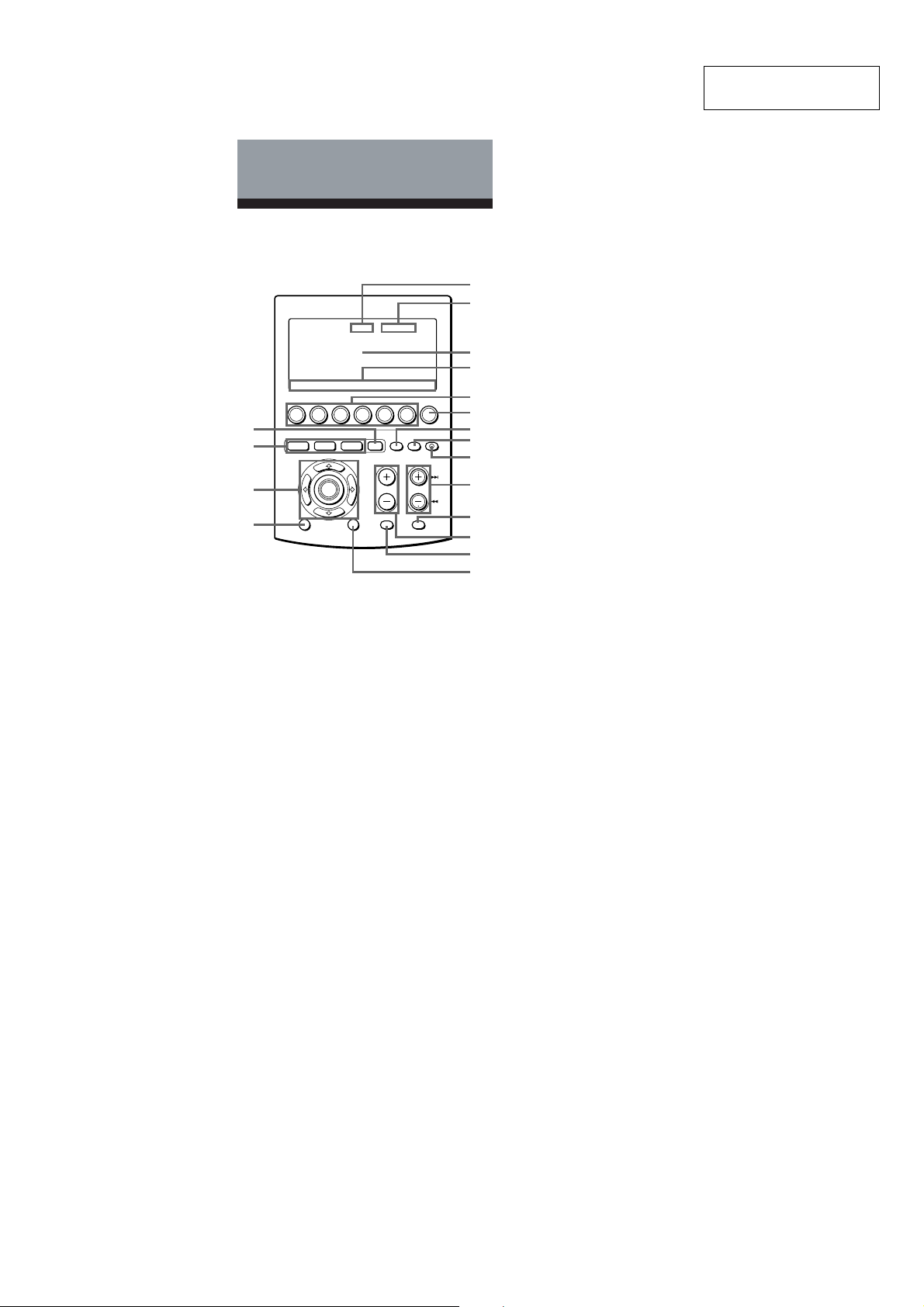
of Controls
1
2
3
4
5
TIMER LIGHT
CHANNELVOLUME
MUTING RECALL
OTHER
COMMANDER
OFF
6
7
8
9
q;
qa
qs
qd
qf
TV STB VCR DVD CD AMP
qk
qj
qh
qg
SYSTEM CONTROL
OK
MENU EXIT
MORE321
1 Clock Display key (page 8)
Displays the clock, the transmission
mark, the battery mark and the timer
mark.
2 Mode Display key (page 8, 13, 20, 30,
32, 40)
Displays the status of the selected
mode.
Function of the key changes according
to the selected mode.
3 LCD touch key display
The keys used for operating each
component and setting the
Commander are displayed.
Note
Do not press the touch keys using sharp
objects such as pins or ball-point pens.
This section is extracted
from instruction manual.
4 Label keys (page 8, 13, 20, 23, 30,
32, 40, 79)
The selected modes (up to 8 characters
in each Label key) are displayed.
Labels change in the order from the
first stage to the third stage and come
back to the first, and so on, each time
you press the Mode Display key,
OTHER, MORE, or TIMER button
according to the selected mode.
5 Component Select buttons (page 12)
Selects the component to control.
6 OTHER button (page 13)
Label keys change in the order from
the first stage to the third stage and
come back to the first, and so on, each
time you press the OTHER button
when the selected component name is
displayed on the Label keys.
7 TIMER button (page 68)
Used to set the timer program, and to
set the timer program on or off.
8 LIGHT button (page 76)
Used to light up the LCD display in
the dark. Press the button once to turn
on the light, and once again to turn it
off.
9
COMMANDER OFF button
Turns the power of the Commander
off. Then all the display contents are
turned off.
q;
CHANNEL +/– buttons (page 88, 89,
90, 91)
Select the channel.
qa
RECALL button (page 88)
qs
VOLUME +/– buttons* (page 19, 29)
Adjust the volume.
qd
MUTING button* (page 19, 31)
Mutes the audio. Press the button
once again to resume at the previous
volume.
RM-AV3000
6
3
Page 3
RM-AV3000
qf EXIT button (page 89)
Used to exit the setting menu.
qg MENU button (page 88)
Calls up the menu display of the
buttons or keys that have menu
function.
qh OK button and Cursor Control
buttons (page 9, 64, 88)
qj SYSTEM CONTROL buttons (page 31)
You can program up to 32 consecutive
key operations to each of the three
SYSTEM CONTROL buttons . You can
automatically carry out the entire
program by pressing one button.
qk MORE button (page 32)
Label keys change in the order from
the first stage to the third stage and
come back to the first, and so on, each
time you press the MORE button in
the system mode.
* Note on the VOLUME +/– and
MUTING buttons
The Commander controls or mutes the TV’s
volume when you select a visual component.
The Commander controls or mutes the
amplifier’s volume when you select an audio
component.
You can change this setting also (page 29).
Note on the power on and off of the
display of the Commander
To turn on the display, press any button except
the COMMANDER OFF button.
To turn off the display, press COMMANDER
OFF, or if you don’t use the Commander, the
display automatically turns off after 10
minutes. This interval can also be changed
(page 74).
Setting the Clock
Setting the clock for the first
time after installing batteries
For the first time after installing batteries,
the Commander is in the clock setting
mode. “CLOCK” is displayed on the
Mode Display key, and “ –:– –” flashes on
the Clock Display key, and “STD TIME”
and “DS TIME” on the Label keys are
flashing.
1
Select STD TIME (standard time)
or DS TIME (daylight saving time).
If the summer time (daylight saving
time) is used in your area, press the
DS TIME key when it is in the
summer time. If not, press the STD
TIME key.
If the summer time is not used in your
area, press the STD TIME key.
or
The selected STD TIME or DS TIME
key lights.
“SET” and “SU” flash and “12:00 AM”
lights on the Clock Display key.
4
Page 4
RM-AV3000
2 Set the day of the week.
Select the day of the week by pressing
or button.
the
Selected day of the week flashes.
SU : Sunday
MO : Monday
TU : Tuesday
WE : Wednesday
TH : Thursday
FR : Friday
SA : Saturday
button
button
3 Set the hour and AM (or PM) by
pressing the
The selected hour and AM (or PM)
flash.
button
Then press the
AM (or PM) are set.
“00”(minute) and “SET” flash.
or button.
button
button.
The hour and
Then press the
the week is set.
“12”, “ AM” and “SET” flash.
Note
If you press the button, the day of the week
is set and setting mode skips to Step 4.
button. The day of
Note
If you press the button, the hour and AM
(or PM) are set and the setting mode
returns to Step 2.
Continued
9
5
Page 5
RM-AV3000
Setting the Clock (continued)
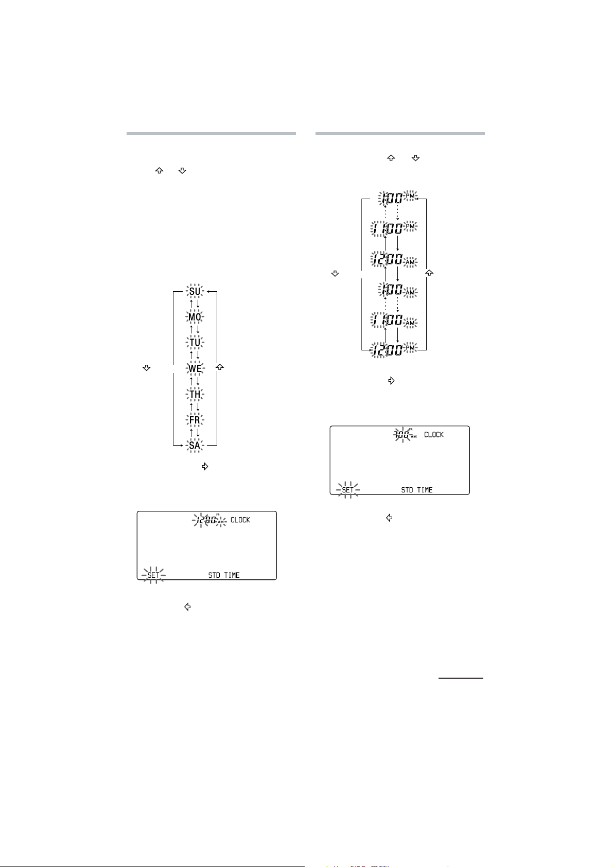
4
Set the minute by pressing the
or button.
button
The selected minute flashes.
button
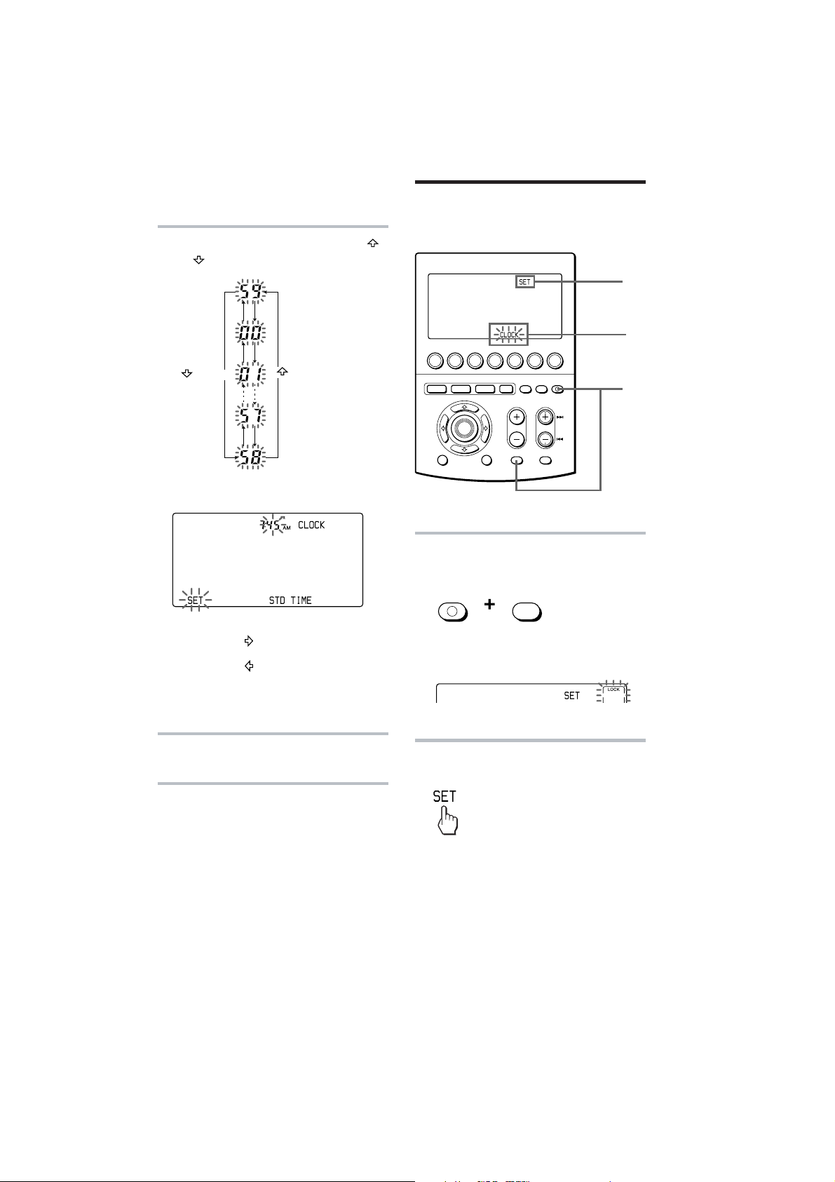
Adjusting the clock after
setting the clock
TIMER LIGHT
CHANNELVOLUME
MUTING RECALL
MUTING
OTHER
COMMANDER
OFF
TV STB VCR DVD CD AMP
SYSTEM CONTROL
MENU EXIT
1
While pressing COMMANDER
MORE321
OK
OFF, press MUTING.
COMMANDER
OFF
2
3
1
Notes
• If you press the button, the minute is set
and the setting mode returns to Step 2.
• If you press the
and the setting mode returns to Step 3.
• If you want to finish the clock setting, go to
Step 5.
5
Press the SET key.
button, the minute is set
The clock starts from 0 second.
Note
If you press the SET key in any step above, the
clock is set then. The clock starts from 0
seconds.
10
“SET” appears on the Mode Display
key.
2
Press the Mode Display key (SET)
twice.
6
Page 6
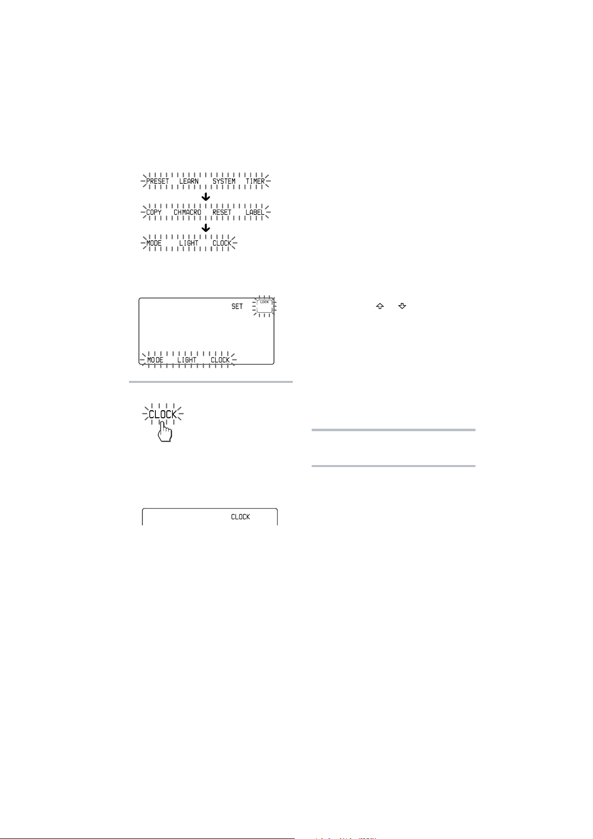
RM-AV3000
Each time the SET key is pressed, the
Label keys change as follows.
“CLOCK” appears and flashes on one
of the Label keys on the display.
3
Press the CLOCK key.
To select STD TIME (standard
time) or DS TIME (daylight
saving time)
When the Commander enters the clock
setting mode when the clock is already
set, the time mode previously set (STD
TIME or DS TIME) stays lit and the other
time mode flashes, and the setting mode
goes to Step 4.
If you want to change the time mode, press
the flashing key (STD TIME or DS TIME).
The selected STD TIME or DS TIME key
lights, and the setting mode goes to Step 4.
If you do not want to change the time
mode, press the
setting mode goes to Step 4.
When the time mode is changed from
STD TIME to DS TIME
The time of the clock returns by one hour.
When the time mode is changed from
DS TIME to STD TIME
The time of the clock advances by one hour.
or button. The
The Commander enters clock setting
mode.
“CLOCK” appears on the Mode Display
key and the current time flashes.,
4
To set the clock, follow Steps 2 - 5
on page 9-10.
Note
If you press the SET key in Step 3 or 4, the
clock is set then. The clock starts from 0 second.
11
7
Page 7

RM-AV3000
)
)
SECTION 2
DISASSEMBLY
Note: Follow the disassembly procedure in the numerical order given.
2-1. Case (lower)
two claws
case (upper)
4 two screws
(B 1.7 × 5)
5
two claws
2 battery case lid
2-2. SUB Board
1
rubber key
1
3 four screws
(+BTP 2 × 6)
4
two screws
(+BTP 2
case (upper
claw
case (lower)
6
case (lower)
×
6)
5
LCD section
3
screw
(+BTP 2
8
×
6)
7
SUB board
6
lead wire 14p
case (lower)
2
two screws
(+BTP 2
×
6
Page 8

2-3. MAIN Board and LCD Unit
)
3
flexible board
(CN2)
MAIN board
7
5
two claws
1
two screws
(+BTP 2
6
two claws
RM-AV3000
×
6)
8
four screws
(+BTP 2
9
holder (B)
×
6)
qs
electro luminescent
2
connector
(CN4)
qd
holder (A)
qa
qf
touch panel
q;
LCD unit
4
flexible board (CN1
9
Page 9

RM-AV3000
SECTION 3
TEST MODE
3-1. EEPROM Check
Connection Method:
Regulated power supply
(+6V constant voltage output)
set
1) While pressing at the same time the [VOLUME -] key and the
[CHANNEL -] key, turn on the main power of the regulated power
supply (DC +6V).
2) After sounding buzzer, Fig.3-1 is displayed.
3) In order to escape from this mode, the [VOLUME -] key and the
[CHANNEL -] key are pushed simultaneously again.
4) After sounding buzzer, EEPROM is initialized and clock setting
mode is displayed.
5) For ending this mode, the [COMMANDER OFF] key is pushed
two seconds or more.
+
–
VER-X
3-2. LCD, All Keys and EL Check
Connection Method:
Regulated power supply
(+6V constant voltage output)
set
1) While pressing at the same time the [VOLUME +] key and the
[CHANNEL +] key, turn on the main power of the regulated power
supply (DC +6V).
2) After sounding buzzer, EL is light up and LCD carries out allpoints light.
3) A code is transmitted to all keys.
4) A push on the [MORE] key changes the display of a dot charactor
portion.
5) A push on the [LIGHT] key changes lighting of EL.
6) A push on the [OTHER] key changes the display of the segment
section.
7) In order to escape from this mode, the [VOLUME +] key and the
[CHANNEL +] key are pushed simultaneously again.
8) After buzzer sound turns two, clock setting mode is displayed.
9) For ending this mode, the [COMMANDER OFF] key is pushed
two seconds or more.
+
–
EEPROM TEST OK
Fig.3-1
10
Page 10

SECTION 4
DIAGRAMS
4-1. IC Pin Function
• IC1 (µPD703033AGF-A27-3BA) (SYSTEM CONTROL)
RM-AV3000
Pin No. Pin Name I/O Pin Description
1 P14 I Segment signal input
2 P15 – Not used
3, 4 P20, 21 I Signal input from EEPROM
5 P22 – Not used
6 P23 I Serial input
7 P24 – Not used
8 P25 I Signal input from EEPROM
9 EVDD – Power supply
10 EVSS – Ground terminal
11 P26 O Buzzer clock output
12 P27 – Not used
13, 14 P30, 31 I Remote control signal received input
15, 16 P32, 33 I Signal input from EEPROM
17 P34 O Remote control signal received output
18, 19 P35, 36 – Not used
20 P37 O Segment signal output
21 IC – Ground terminal
22 to 29 P100 to P107 I Segment signal intput
30 to 33 P110 to P113 I Segment signal intput
34 RESET I System reset input
35 XT1 I Crystal (Sub system clock)
36 XT2 O Crystal (Sub system clock)
37 REGC – Not used
38 X2 O Crystal (Main system clock)
39 X1 I Crystal (Main system clock)
40 VSS – Ground terminal
41 VDD – Power supply
42 CLK OUT – Not used
43 P90 O EL control output (bright)
44 P91 O EL control output (dark)
45 to 49 P92 to P96 – Not used
50 P40 – Fixed at “L”
51 to 57 P41 to P47 O Segment signal output
58 BVDD – Power supply
59 BVSS – Ground terminal
60 to 63 P50 to P53 O LCD power supply
64 to 67 P54 to P57 – Not used
68 P60 O LCD power control output
69 P61 – Not used
70 to 73 P62 to P65 O Segment signal output
74 AVDD – Not used
75 AVSS – Ground terminal
76 AVREF – Fixd at “L”
77 to 84 P70 to P77 – Fixd at “L”
85 to 88 P80 to P83 – Fixd at “L”
89, 90 P00, P01 – Not used
91 P02 O Remote control signal received clock ON/OFF output
92, 93 P03, 04 – Not used
94 P05 – Power supply
95, 96 P06, 07 – Not used
97 to 100 P10 to P13 I Segment signal input
Note on Schematic Diagram:
• All capacitors are in µF unless otherwise noted. p: pF.
50 WV or less are not indicated except for electrolytics and
tantalums.
• All resistors are in Ω and 1/
fied.
f
•
• C : panel designation.
• A : B+ Line.
•Power voltage is dc 6.0V and fed with regulated dc power sup-
•Voltages and waveforms are dc with respect to ground under
•Voltages are taken with a VOM (Input impedance 10 MΩ).
: internal component.
ply from battery terminal.
no-signal conditions.
Voltage variations may be noted due to normal production tolerances.
4
W or less unless otherwise speci-
•Waveforms
1
IC1 ek
(TPX1)
4.6 Vp-p
500 ms
2
IC1 eh
(TPX2)
30.5 µs
100ns
3.6Vp-p
4.3Vp-p
•Waveforms are taken with a oscilloscope.
• Circled numbers refer to waveforms.
Note on Printed Wiring Board:
• X : parts extracted from the component side.
• Y : parts extracted from the conductor side.
• : Pattern from the side which enables seeing.
(The other layers' patterns are not indicated.)
• : Carbon pattern
Caution:
Pattern face side: Parts on the pattern face side seen from
(Conductor Side) the pattern face are indicated.
Parts face side: Parts on the parts face side seen from
(Component Side) the parts face are indicated.
1111
Page 11

RM-AV3000
4-2. Printed Wiring Board — MAIN Board —
MAIN BOARD
R26
TO
EL
(COMPONENT SIDE)
IC6
IC7
✩
✩ D7, IC1 and L1 have not carried out supply with a single article.
These become supply by mounted MAIN board (A-3178-728-A).
TO
TOUCH-PAD
✩
R16
R15
BZ1
R3
R5
C3
IC5
R6
IC8
R9
MAIN BOARD
(CODUCTOR SIDE)
C16
Q8
D9
• Semiconductor
Q5
Location
Ref. No. Location
D1 A-4
D2 A-3
D3 A-2
D4 A-1
D5 D-1
D7 A-3
D9 D-1
IC1 C-2
Q6
R19
A
TO
SUB BOARD
Ref. No. Location
IC2 C-4
IC3 C-4
IC5 B-3
IC6 B-2
IC7 B-2
IC8 B-3
Q1 A-4
Q2 B-1
✩
IC1
Ref. No. Location
Q3 B-3
Q4 D-1
Q5 D-1
Q6 C-1
Q8 D-1
Q11 D-4
R51
R52
R56
R50
R54
TO
LCD MODULE
IC2
IC3
R53
1-685-020-
R55
R57
11
(11)
11
(11)
1-685-020-
1212
Page 12

RM-AV3000
4-3. Schematic Diagram — MAIN Board —
✩ D7, IC1 and L1 have not carried out supply with a single article.
These become supply by mounted MAIN board (A-3178-728-A).
CAT24WG256KI
-1.8-TE13
TP14
-RTX
1
CAT24WG256KI
-1.8-TE13
A-TX
A-TX
A-TX
A-TX
1313
Page 13

RM-AV3000
4-4. Printed Wiring Board — SUB Board — 4-5. Schematic Diagram — SUB Board —
1414
Page 14

NOTE:
• -XX, -X mean standardized parts, so they may
have some differences from the original one.
• Items marked “*” are not stocked since they
are seldom required for routine service. Some
delay should be anticipated when ordering these
items.
#1
SECTION 5
EXPLODED VIEWS
• The mechanical parts with no reference number
in the exploded views are not supplied.
14
13
RM-AV3000
15
12
a
11
#1
10
8
5
7
#1
a
16
#1
17
9
6
18
3
19
2
#1
5
20
#1
#1
4
1
Ref. No. Part No. Description Remarks Ref. No. Part No. Description Remarks
1 3-242-714-01 LID, BATTERY CASE
2 3-242-713-01 CASE (LOWER)
3 3-243-827-01 TERMINAL (B), COMMONNESS
4 3-740-607-01 CUSHION
5 3-243-826-01 TERMINAL (A), COMMONNESS
6 3-242-715-01 FILTER, LED
7 3-243-829-01 TERMINAL (-), BATTERY
8 3-243-828-01 TERMINAL (+), BATTERY
* 9 1-824-402-11 WIRE, LEAD (WITH CONNECTOR)14P
* 10 1-685-021-11 SUB BOARD
11 3-242-716-01 KEY, RUBBER
* 12 A-3178-728-A MAIN BOARD, COMPLETE
13 3-242-718-01 HOLDER (B)
14 3-242-712-01 CASE (UPPER)
15 3-318-203-72 SCREW (B1.7X5), TAPPING
16 3-242-842-01 DAMPER
17 1-417-320-11 PANEL, TOUCH
18 3-242-717-01 HOLDER (A)
19 1-477-440-11 LCD UNIT
20 1-758-811-11 ELECTRO LUMINESCENT
#1 7-685-504-19 SCREW +BTP 2X6 TYPE2 N-S
15
Page 15

RM-AV3000
MAIN
SECTION 6
ELECTRICAL PARTS LIST
NOTE:
• Due to standardization, replacements in the
parts list may be different from the parts
specified in the diagrams or the components
used on the set.
• -XX, -X mean standardized parts, so they
may have some difference from the original
one.
• Items marked “*” are not stocked since they
are seldom required for routine service.
Some delay should be anticipated when
ordering these items.
Ref. No. Part No. Description Remarks Ref. No. Part No. Description Remarks
* A-3178-728-A MAIN BOARD, COMPLETE
*********************
• CAPACITORS:
uF: µF
• RESISTORS
All resistors are in ohms.
METAL: metal-film resistor
METAL OXIDE: Metal Oxide-film resistor
F: nonflammable
• COILS
uH: µH
IC7 8-759-578-59 IC S-80845ALNP-EA9-T2
IC8 6-702-700-01 IC S-80840ANNP-ED4-T2
• SEMICONDUCTORS
In each case, u: µ, for example:
uA...: µA... , uPA... , µPA... ,
uPB... , µPB... , uPC... , µPC... ,
uPD..., µPD...
When indicating parts by reference number,
please include the board name.
3-242-717-01 HOLDER (A)
3-242-718-01 HOLDER (B)
7-685-504-19 SCREW +BTP 2X6 TYPE2 N-S
< BUZZER >
BZ1 1-825-190-11 BUZZER
< CAPACITOR >
C1 1-164-230-11 CERAMIC CHIP 220PF 5.00% 50V
C2 1-162-967-11 CERAMIC CHIP 0.0033uF 10% 50V
C3 1-165-176-11 CERAMIC CHIP 0.047uF 10.00% 16V
C4 1-165-176-11 CERAMIC CHIP 0.047uF 10.00% 16V
C5 1-162-970-11 CERAMIC CHIP 0.01uF 10% 25V
C6 1-104-665-11 ELECT 100uF 20.00% 10V
C7 1-126-935-11 ELECT 470uF 20.00% 10V
C8 1-162-970-11 CERAMIC CHIP 0.01uF 10% 25V
C10 1-162-970-11 CERAMIC CHIP 0.01uF 10% 25V
C11 1-162-970-11 CERAMIC CHIP 0.01uF 10% 25V
C14 1-126-935-11 ELECT 470uF 20.00% 10V
C15 1-126-964-11 ELECT 10uF 20.00% 50V
C16 1-107-826-11 CERAMIC CHIP 0.1uF 10.00% 16V
C17 1-162-919-11 CERAMIC CHIP 22PF 5% 50V
C18 1-162-919-11 CERAMIC CHIP 22PF 5% 50V
C22 1-165-176-11 CERAMIC CHIP 0.047uF 10.00% 16V
< CONNECTOR >
* CN2 1-816-747-11 CONNECTOR 4P
* CN3 1-816-746-11 CONNECTOR 14P
* CN4 1-816-745-11 CONNECTOR 20P
< DIODE >
D1 8-719-077-83 DIODE SLR-938CV-K-BC
D2 8-719-058-59 DIODE SE303AY
D3 8-719-058-59 DIODE SE303AY
D4 8-719-077-83 DIODE SLR-938CV-K-BC
D5 8-719-820-61 DIODE 1SS294-TE85L
✩ D7 ---------------- DIODE TPS705
D9 8-719-820-61 DIODE 1SS294-TE85L
< IC >
✩ IC1 ---------------- IC uPD703033AGF-A27-3BA
IC2 6-701-000-01 IC CAT24WG256KI-1.8-TE13
IC3 6-701-000-01 IC CAT24WG256KI-1.8-TE13
IC5 8-759-932-92 IC TC4069UBF-TP1
IC6 8-759-512-51 IC RH5RE50AA-T1
< TRANSFORMER >
✩ L1 ---------------- TRANSFORMER, INVERTER
< WIRE >
* JP1 1-824-403-11 WIRE, LEAD (WITH CONNECTOR)20P
< TRANSISTOR >
Q1 8-729-420-68 TRANSISTOR 2SD1328-R-TX
Q2 8-729-420-68 TRANSISTOR 2SD1328-R-TX
Q3 8-729-018-55 TRANSISTOR 2SD6O2A-TX
Q4 8-729-018-55 TRANSISTOR 2SD6O2A-TX
Q5 8-729-018-55 TRANSISTOR 2SD6O2A-TX
Q6 8-729-420-68 TRANSISTOR 2SD1328-R-TX
Q8 8-729-018-55 TRANSISTOR 2SD6O2A-TX
Q11 8-729-400-45 TRANSISTOR 2SB7O9-RTX
< RESISTOR >
R1 1-218-867-11 RES-CHIP 6.8K 5% 1/10W
R2 1-216-833-11 METAL CHIP 10K 5% 1/16W
R3 1-216-833-11 METAL CHIP 10K 5% 1/16W
R4 1-216-861-11 METAL CHIP 2.2M 5% 1/16W
R5 1-216-840-11 METAL CHIP 39K 5% 1/16W
R6 1-216-818-11 METAL CHIP 560 5% 1/16W
R7 1-216-838-11 METAL CHIP 27K 5% 1/16W
R8 1-216-846-11 METAL CHIP 120K 5% 1/16W
R9 1-216-845-11 METAL CHIP 100K 5% 1/16W
R10 1-216-845-11 METAL CHIP 100K 5% 1/16W
R11 1-216-851-11 METAL CHIP 330K 5% 1/16W
R15 1-216-829-11 METAL CHIP 4.7K 5% 1/16W
R16 1-216-821-11 METAL CHIP 1K 5% 1/16W
R19 1-216-821-11 METAL CHIP 1K 5% 1/16W
R20 1-216-821-11 METAL CHIP 1K 5% 1/16W
R21 1-216-825-11 METAL CHIP 2.2K 5% 1/16W
R22 1-216-805-11 METAL CHIP 47 5% 1/16W
R23 1-216-817-11 METAL CHIP 470 5% 1/16W
R24 1-216-817-11 METAL CHIP 470 5% 1/16W
R25 1-216-148-00 RES-CHIP 8.2 5% 1/8W
R26 1-216-148-00 RES-CHIP 8.2 5% 1/8W
R33 1-216-817-11 METAL CHIP 470 5% 1/16W
R37 1-216-833-11 METAL CHIP 10K 5% 1/16W
R40 1-216-833-11 METAL CHIP 10K 5% 1/16W
R41 1-216-833-11 METAL CHIP 10K 5% 1/16W
✩ D7, IC1 and L1 have not carried out supply with a single
article. These become supply by mounted MAIN board
(A-3178-728-A).
16
Page 16

Ref. No. Part No. Description Remarks
R42 1-216-837-11 METAL CHIP 22K 5% 1/16W
R43 1-216-845-11 METAL CHIP 100K 5% 1/16W
R50 1-216-841-11 METAL CHIP 47K 5% 1/16W
R51 1-216-841-11 METAL CHIP 47K 5% 1/16W
R52 1-216-837-11 METAL CHIP 22K 5% 1/16W
R53 1-216-841-11 METAL CHIP 47K 5% 1/16W
R54 1-216-837-11 METAL CHIP 22K 5% 1/16W
R55 1-216-841-11 METAL CHIP 47K 5% 1/16W
R56 1-216-837-11 METAL CHIP 22K 5% 1/16W
R57 1-216-841-11 METAL CHIP 47K 5% 1/16W
< VIBRATOR >
X1 1-579-175-11 VIBRATOR, CERAMIC (10MHz)
X2 1-527-997-21 VIBRATOR, CRYSTAL (32.768kHz)
************************************************************
RM-AV3000
SUBMAIN
* 1-685-021-11 SUB BOARD
* 1-824-402-11 WIRE, LEAD (WITH CONNECTOR)14P
3-243-828-01 TERMINAL (+), BATTERY
3-243-829-01 TERMINAL (-), BATTERY
***********************************************************
17 1-477-440-11 LCD UNIT
***********************************************************
3-242-704-13 MANUAL, INSTRUCTION (ENGLISH)
3-242-704-22 MANUAL, INSTRUCTION (SPANISH) (US)
3-242-704-32 MANUAL, INSTRUCTION (FRENCH) (CND)
**********
MISCELLANEOUS
***************
ACCESSORIES
************
17
Page 17

RM-AV3000
REVISION HISTORY
Clicking the version allows you to jump to the revised page.
Also, clicking the version at the upper right on the revised page allows you to jump to the next revised
page.
Ver. Date Description of Revision
1.0 2002.05 New
1.1 2004.09 Correction of a photograph on P.1 (SPM-04118)
 Loading...