

Page 1
PMC-MD55
SERVICE MANUAL
Ver 1.0 1999. 06
U.S. and foreign patents licensed form Dolby Laboratories
Licensing Corporation.
CD
Section
MD
Section
US Model
Model Name Using Similar Mechanism NEW
CD Mechanism Type KSM-213CGP
Optical Pick-up Name KSS-213C
Model Name Using Similar Mechanism MDS-JB920
MD Mechanism Type MDM-5A
Base Unit Name MBU-5A
Optical Pick-up Name KMS-260A
SPECIFICATIONS
PERSONAL
MICROFILM
MINIDISC SYSTEM
Page 2

TABLE OF CONTENTS
1. SERVICING NOTES .............................................. 3
2. GENERAL
Playing a CD .................................................................. 6
Recording a Whole CD .................................................. 6
Playing an MD ............................................................... 7
Listening to the radio ..................................................... 7
Setting the Clock ............................................................ 8
Hooking up the System.................................................. 8
3. DISASSEMBLY ........................................................ 9
4. TEST MODE............................................................. 15
5. ELECTRICAL ADJUSTMENTS
Tuner Section ................................................................. 20
MD Section .................................................................... 21
CD Section ..................................................................... 28
Display Section .............................................................. 30
6. DIAGRAMS
6-1. Block Diagram – TUNER Section – ............................ 31
6-2 Block Diagram – MD Section – ................................... 34
6-3. Block Diagram – CD Section – .................................... 37
6-4. Block Diagram
– FUNCTION SELECT/PANEL Section –................... 40
6-5. Block Diagram
– POWER AMP/POWER SUPPLY Section – .............. 43
6-6. Block Diagram – SUPER WOOFER Section – ........... 45
6-7. Printed Wiring Board – TUNER Section – .................. 49
6-8. Schematic Diagram – TUNER Section – ..................... 51
6-9. Schematic Diagram – BD Section – ............................. 53
6-10. Printed Wiring Boards – BD Section – ........................ 57
6-11. Printed Wiring Board – DG Section –.......................... 59
6-12. Schematic Diagram – DG Section –............................. 61
6-13. Printed Wiring Boards – MAIN Section – ................... 64
6-14. Schematic Diagram – MAIN (CD) Section – .............. 67
6-15. Schematic Diagram
– MAIN (SYSTEM CONTROL) Section – .................. 70
6-16. Schematic Diagram
– MAIN (FUNCTION SELECT) Section – .................. 73
6-17. Printed Wiring Board – AUDIO/JACK Section –........ 75
6-18. Schematic Diagram – AUDIO/JACK Section – .......... 77
6-19. Schematic Diagram – CD MOTOR Section – ............. 79
6-20. Printed Wiring Board – CD MOTOR Section – .......... 81
6-21. Printed Wiring Board
– CD OPEN/CLOSE Section –...................................... 82
6-22. Schematic Diagram – CD OPEN/CLOSE Section – ... 83
6-23. Printed Wiring Boards – PANEL Section – ................. 86
6-24. Schematic Diagram – PANEL Section – ...................... 89
6-25. Printed Wiring Boards
– POWER AMP/POWER Section – .............................. 91
6-26. Schematic Diagram
– POWER AMP/POWER Section – .............................. 93
6-27. Printed Wiring Boards
– SUPER WOOFER Section – ...................................... 95
6-28. Schematic Diagram
– SUPER WOOFER Section – ...................................... 97
6-29. IC Pin Function Description .......................................... 108
7. EXPLODED VIEWS ............................................... 118
8. ELECTRICAL PARTS LIST ..............................128
SAFETY-RELATED COMPONENT WARNING!!
COMPONENTS IDENTIFIED BY MARK ! OR DOTTED
LINE WITH MARK ! ON THE SCHEMA TIC DIAGRAMS
AND IN THE PARTS LIST ARE CRITICAL TO SAFE
OPERATION. REPLACE THESE COMPONENTS WITH
SONY PARTS WHOSE PART NUMBERS APPEAR AS
SHOWN IN THIS MANUAL OR IN SUPPLEMENTS PUBLISHED BY SONY.
CAUTION
Use of controls or adjustments or performance of procedures
other than those specified herein may result in hazardous radiation exposure.
This appliance is classified as a CLASS 1 LASER product.
The CLASS 1 LASER PRODUCT MARKING is located on
the rear exterior.
Laser component in this product is capable of emitting radiation
exceeding the limit for Class 1.
– 2 –
Page 3
SECTION 1
SERVICING NOTES
SAFETY CHECK-OUT
After correcting the original service problem, perform the following safety check before releasing the set to the customer:
Check the antenna terminals, metal trim, “metallized” knobs,
screws, and all other exposed metal parts for AC leakage.
Check leakage as described below.
LEAKAGE TEST
The AC leakage from any exposed metal part to earth ground and
from all exposed metal parts to any exposed metal part having a
return to chassis, must not exceed 0.5 mA (500 microamperes).
Leakage current can be measured by any one of three methods.
1. A commercial leakage tester, such as the Simpson 229 or RCA
WT -540A. Follo w the manufacturers’ instructions to use these
instruments.
2. A battery-operated AC milliammeter. The Data Precision 245
digital multimeter is suitable for this job.
3. Measuring the voltage drop across a resistor by means of a
VOM or battery-operated AC voltmeter. The “limit” indication is 0.75 V, so analog meters must have an accurate lowvoltage scale. The Simpson 250 and Sanwa SH-63Trd are examples of a passive VOM that is suitable. Nearly all battery
operated digital multimeters that have a 2 V A C range are suitable. (See Fig. A)
To Exposed Metal
Parts on Set
NOTES ON HANDLING THE OPTICAL PICK-UP
BLOCK OR BASE UNIT
The laser diode in the optical pick-up block may suffer electrostatic break-down because of the potential difference generated
by the charged electrostatic load, etc. on clothing and the human
body.
During repair, pay attention to electrostatic break-down and also
use the procedure in the printed matter which is included in the
repair parts.
The flexible board is easily damaged and should be handled with
care.
NOTES ON LASER DIODE EMISSION CHECK
The laser beam on this model is concentrated so as to be focused
on the disc reflective surface by the objective lens in the optical
pick-up block. Therefore, when checking the laser diode emission, observe from more than 30 cm away from the objective lens.
Notes on chip component replacement
• Never reuse a disconnected chip component.
• Notice that the minus side of a tantalum capacitor may be damaged by heat.
Flexible Circuit Board Repairing
• Keep the temperature of the soldering iron around 270 ˚C during repairing.
• Do not touch the soldering iron on the same conductor of the
circuit board (within 3 times).
• Be careful not to apply force on the conductor when soldering
or unsoldering.
AC
1.5 k
0.15 µF
Fig. A. Using an AC voltmeter to check AC leakage.
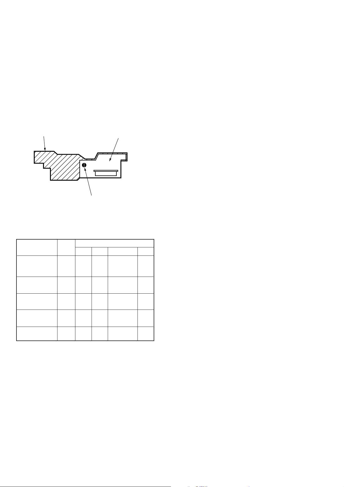
CHUCK PLATE JIG ON REPAIRING
On repairing CD section, playing a disc without the CD lid, use
Chuck Plate Jig.
• Code number of Chuck Plate Jig: X-4918-255-1
Ω
Earth Ground
voltmeter
(0.75 V)
– 3 –
Page 4
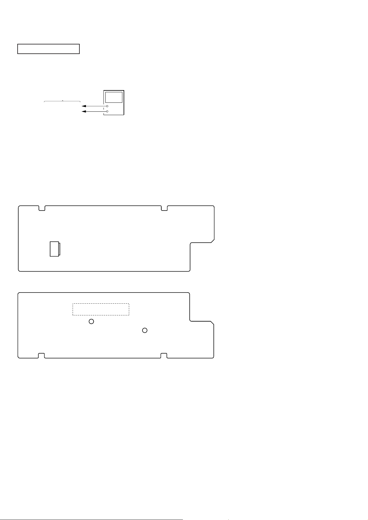
JIG FOR CHECKING BD BOARD WAVEFORM
r
The special jig (J-2501-149-A) is useful for checking the waveform of the BD board. The names of terminals and the checking items to be
performed are shown as follows.
GND: Ground
I+3V : For measuring IOP (Check the deterioration of the optical pick-up laser)
IOP : For measuring IOP (Check the deterioration of the optical pick-up laser)
TEO : TRK error signal (Traverse adjustment)
VC : Reference level for checking the signal
RF : RF signal (Check jitter)
Mechanism deck
RF
VC
TEO
IOP
I+3V
GND
RF
VC
TEO
IOP
I+3V
GND
5P Connector
CN110
6P connecto
for MDM-3
1
5
for MDM-5
1
6
RF
VC
TEO
IOP
I+3V
VC
RF
TEO
IOP
I+3V
GND
– 4 –
Page 5

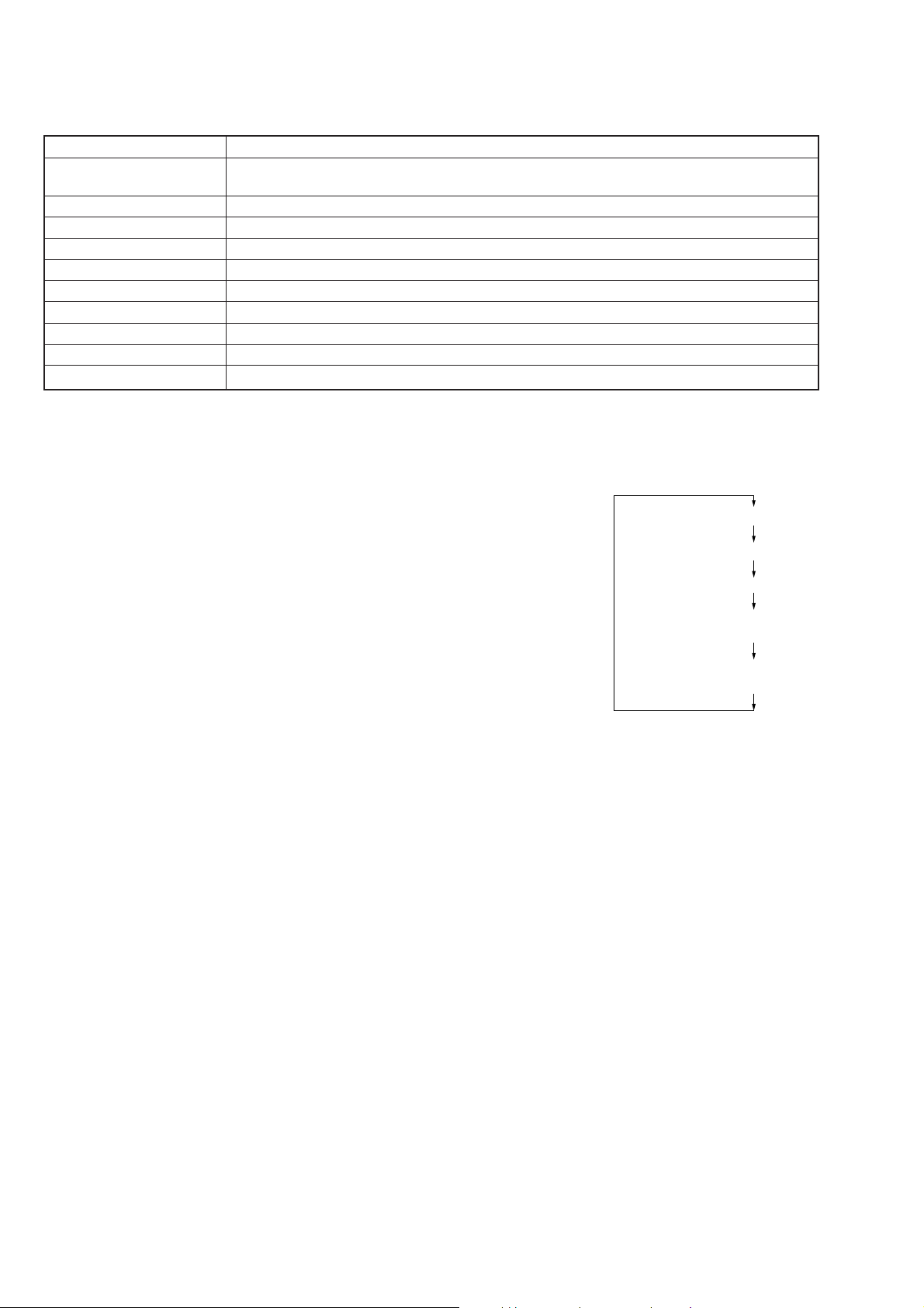
CHECKS PRIOR TO PARTS REPLACEMENT AND ADJUSTMENTS (for MD Section)
Before performing repairs, perform the following checks to determine the faulty locations up to a certain extent.
Details of the procedures are described in “5 Electrical Adjustments”.
Laser power check
(6-1 : See page 23)
Focus bias check
(6-2 : See page 23)
C PLAY check
(6-3 : See page 23)
Self-recording/playback
check
(6-4 : See page 23)
Criteria for Determination
(Unsatisfactory if specified value is not satisfied)
• 0.9 mW power
Specified value : 0.84 to 0.92 mW
• 7.0 mW power
Specified value : 6.8 to 7.2 mW
lop (at 7mW)
• Labeled on the optical pickup
Iop value ± 10mA
• Error rate check
Specified value : For points a, b, and c
C1 error : About 200
ADER : Below 2
• Error rate check
Specified value:
a. When using test disc (MDW-74/AU-1)
C1 error : Below 80
ADER : Below 2
b. When using check disc (TDYS-1)
C1 error : Below 50
• CPLAY error rate check
Specified value:
C1 error : Below 80
ADER : Below 2
• Clean the optical pick-up
• Adjust again
• Replace the optical pick-up
• Replace the optical pick-up
• Replace the optical pick-up
• Replace the optical pick-up
If always unsatisfactory:
• Replace the overwrite head
• Check for disconnection of the circuits around the
overwrite head
If occasionally unsatisfactory:
• Check if the overwrite head is distorted
• Check the mechanism around the sled
Measure if unsatisfactory:
Note:
The criteria for determination above is intended merely to determine if satisfactory or not, and does not serve as the specified value for
adjustments.
When performing adjustments, use the specified values for adjustments.
– 5 –
Page 6
SECTION 2
GENERAL
This section is extracted from
instruction manual.
– 6 –
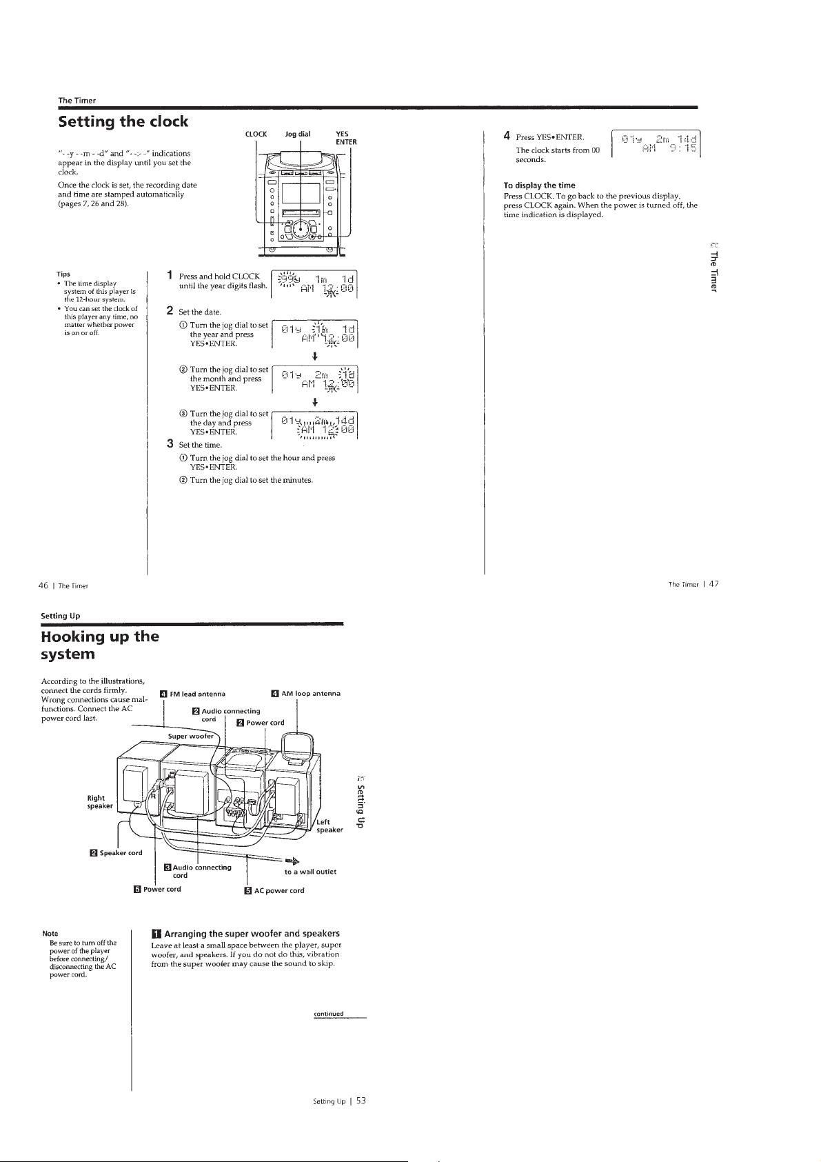
Page 7
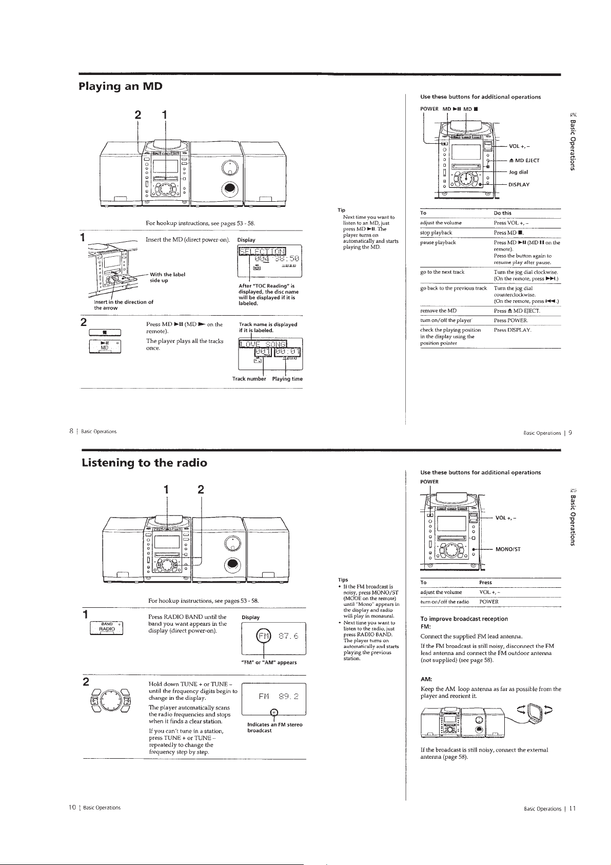
– 7 –
Page 8
– 8 –
Page 9
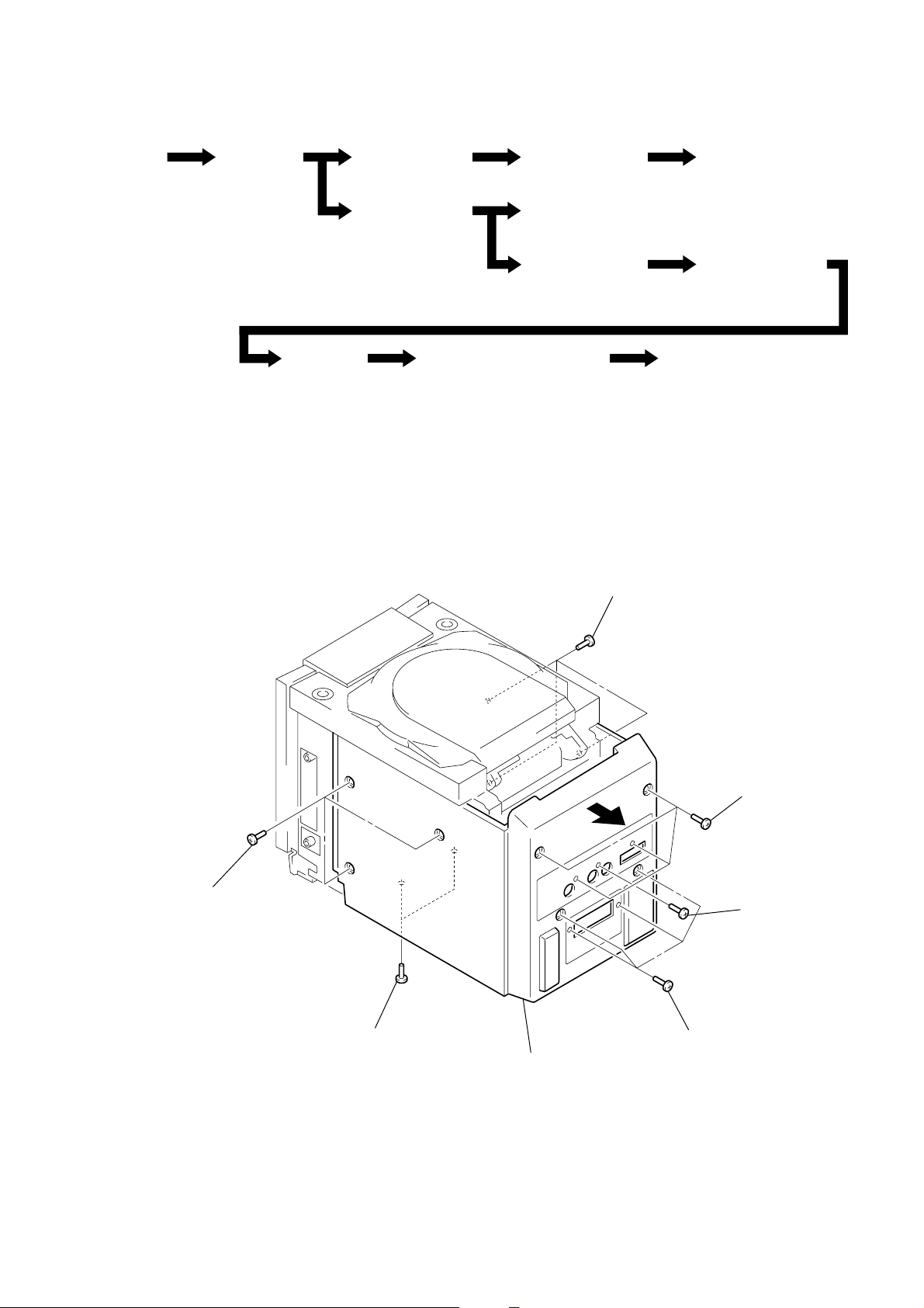
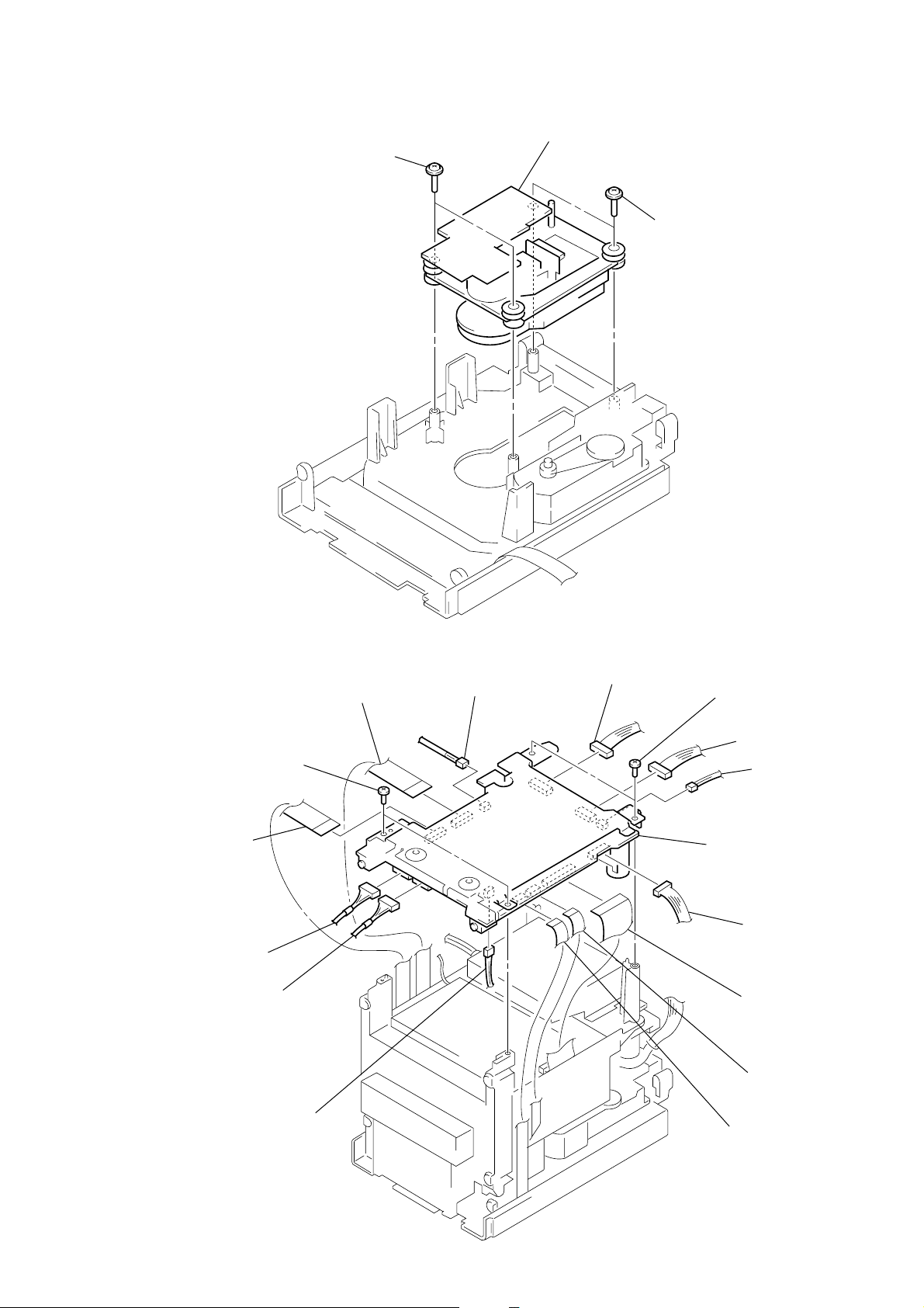
DISASSEMBLY
)
)
• This set can be disassembled in the order shown below.
SECTION 3
Set Rear cabinet Front cabinet block
Main board section Main board
Slider (CAM) Base unit (MBU-5A), BD board SW board, loading motor (M103)
Note: Follow the disassembly procedure in the numerical order given.
REAR CABINET
Upper cabinet block CD PICK-UP assy
TU block, MD block MD mechanism deck
1
three screws
(BTP2.6
×
8)
1
three screws
(BTP2.6
3
four screws
×
10
(BTP3
3
×
10)
screw
(BTP3
×
10
×
8)
2
two screws
×
(BVTT3
8)
4
rear cabinet
3
four screws
(BTP3
– 9 –
Page 10
FRONT CABINET BLOCK
)
2
harness
1
three screws
(BVTP3
×
12)
1
three screws
(BVTP3
×
12
4
cabinet
(front) block
UPPER CABINET BLOCK
1
connector (CN711)
3
wire, parallel (ffc) 12P
(CN407)
3
cabinet (upper) block
1
wire, parallel (ffc) 16P
(from OPTICAL PICK-UP connector)
1
wire, parallel (ffc) 11P
(CN1001)
1
wire, parallel (ffc) 8P
(CN409)
– 10 –
2
three claws
Page 11
CD PICK-UP ASSY
)
P
1
two screws
(PWH2.6
×
10)
2
PICK-UP assy
1
two screws
(PWH2.6
×
10)
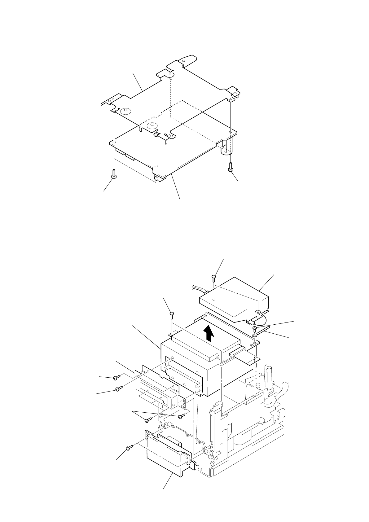
MAIN BOARD SECTION
3
two screws
2
wire parallel (ffc) 11P
(CN702)
1
(BVTP3
connector
(CN408)
1
connector
(CN402)
×
2
wire parallel (ffc) 16P
(CN701)
10)
1
connector
(CN704)
1
connector
(CN302)
3
two screws
(BVTP3
4
main board section
×
1
connector (CN303)
1
connector (CN401
1
connector (CN404)
2
wire parallel (ffc) 26
(CN405)
2
wire parallel (ffc) 9P
(CN406)
10)
1
connector
(CN312)
– 11 –
2
wire parallel (ffc) 8P
(CN409)
Page 12
MAIN BOARD
)
shield plate (main)
1
two screws
(BVTT2.6
1
two screws
(BVTT2.6
×
6)
2
main board
×
6
TU BLOCK, MD BLOCK
3
screw
(BVTP2.6
4
two screws
(BVTT2.6
×
5
shield plate
(front)
×
8)
5)
3
four screws
(BVTP2.6
0
MD block assy
×
8)
8
two screws
(BVTP3
×
10)
6
two screws
(BVTP3
×
10)
7
TU block assy
9
8
screw
(BVTP3
harness
×
10)
1
two screws
(BVTP2.6
×
10)
2
LCD block assy
– 12 –
Page 13
MD MECHANISM DECK
P
5
two screws
(BVTTWH M3)
7
MD mechanism deck
(MDM-5A)
1
four claws
2
shield plate (upper)
5
4
two screws
(BVTTWH M3)
3
connector
(CN601)
wire, parallel (ffc) 21P
(CN102)
4
wire, parallel (ffc) 23
(CN103)
SLIDER (CAM)
2
bracket (Guide L)
1
two screws (P2.6 × 6)
3
leaf spring
6
slider (Cam)
6
harness
• Note for Installation of Slider A (Cam)
Set the shaft of Cam gear to
be at the position in the figure.
Set the shaft of Lever (O/C) to
be at the position in the figure.
4
two screws (P2.6 × 6)
5
bracket (Guide R)
– 13 –
Page 14
BASE UNIT (MBU-5A), BD BOARD
5
flexible board
(CN104)
6
flexible board
(CN101)
2
1
three screws
(P2.6
base unit (MBU-5A)
×
6)
SW BOARD, LOADING MOTOR (M103)
4
screw (M1.7 × 4)
3
two screws
(PWH1.7
7
BD board
2
×
gear B
4)
3
Remove the solder (Five portion).
1
screw (PTPWH M2.6 × 6)
4
loading motor (M103)
6
SW board
5
three screws (BTP2.6 × 6)
– 14 –
Page 15
SECTION 4
TEST MODE
Refer to “5. ELECTRICAL ADJUSTMENT” for the test mode of CD section.
MD SECTION
1. PRECAUTIONS FOR USE OF TEST MODE
• As loading related operations will be performed regardless of the test mode operations being performed, be sure to check that the disc
is stopped before setting and removing it.
Even if the [MDEJECT] button is pressed while the disc is rotating during continuous playback, continuous recording, etc., the disc
will not stop rotating.
Therefore, it will be ejected while rotating.
Be sure to press the [MDEJECT] button after pressing the [NO,CANCEL] button and the rotation of disc is stopped.
1-1. Recording laser emission mode and operating buttons
• Continuous recording mode (CREC MODE)
• Laser power check mode (LDPWR CHECK)
• Laser power adjustment mode (LDPWR ADJUST)
• When pressing the [REC] button.
2. SETTING THE TEST MODE
1. Set to standby state.
2. While pressing the both [BASS/TREBLE] and [EDIT] buttons, press the button [,MD] n π (MD) n [,MD] n π (MD).
3. Release the both [BASS/TREBLE] and [EDIT] buttons to enter the MD test mode.
3. RELEASING THE TEST MODE
Press the [POWER] button to turn the power OFF, or press the [RESET] (bottom of the player unit) switch.
6
6
flfl
[]
[]
4. BASIC OPERATIONS OF THE TEST MODE
All operations are performed using the JOG dial, [YES,ENTER] button, and [NO,CANCEL] button.
The functions of these buttons are as follows.
Function name Function
JOG dial Changes parameters and modes
YES, ENTER button Proceeds onto the next step. Finalizes input.
NO, CANCEL button Returns to previous step. Stops operations.
– 15 –
Page 16

5. SELECTING THE TEST MODE
There are 9 types of test modes as shown below. The groups can be switched by turning the JOG dial. After selecting the g roup to be used,
press the [YES,ENTER] button. After setting a certain group, turn the JOG dial switches between these modes.
Display
TEMP ADJUST
LDPWR ADJUST
LDPWR CHECK
EFBAL ADJUST
FBIAS ADJUST
FBIAS CHECK
CPLAY MODE
CREC MODE
EEP MODE
• For details of each adjustment mode, refer to “5. Electrical Adjustments”.
• If a different mode has been selected by mistake, press the [NO,CANCEL] button to release that mode.
• EEP MODE is not used for servicing and therefore are not described in detail. If these modes are set accidentally , press the [NO,CANCEL]
button to release the mode immediately. Be especially careful this mode will overwrite the non-volatile memory and reset it, and as a
result, the unit will not operate normally.
Temperature compensation offset adjustment
Laser power adjustment
Laser power check
EF balance adjustment
Focus bias adjustment
Focus bias check
Continuous playback mode
Continuous recording mode
Non-volatile memory control
Contents
– 16 –
Page 17

5-1. Operating the Continuous Playback Mode
1. Entering the continuous playback mode
(1) Set the disc in the unit. (Whichever recordable discs or discs for playback only are available)
(2) Turn the JOG dial and display “CPLAY MODE”.
(3) Press the [YES,ENTER] button to change the display to “CPLAY MID”.
(4) When access completes, the display changes to “C1 = AD = ”.
Note: The numbers “ ” displayed show you error rates and ADER.
2. Changing the parts to be played back
(1) Press the [YES,ENTER] button during continuous playback to change the display as below.
“CPLAY MID” n “CPLAY OUT” n “CPLAY IN”
When pressed another time, the parts to be played back can be moved.
(2) When access completes, the display changes to “C1 = AD = ”.
Note: The numbers “ ” displayed show you error rates and ADER.
3. Ending the continuous playback mode
(1) Press the [NO,CANCEL] button. The display will change to “CPLAY MODE”.
(2) Press the [MDEJECT] button and take out the disc.
Note: The playback start addresses for IN, MID, and OUT are as follows.
IN : 40h cluster
MID : 300h cluster
OUT: 700h cluster
5-2. Operating the Continuous Recording Mode (Use only when performing self-recording/palyback check)
1. Entering the continuous recording mode
(1) Set a recordable disc in the unit.
(2) Turn the JOG dial and display “CREC MODE”.
(3) Press the [YES,ENTER] button to change the display to “CREC MID”.
(4) When access completes, the display changes to “CREC ( )” and “[REC]” lights up.
Note: The numbers “ ” displayed shows you the recording position addresses.
2. Changing the parts to be recorded
(1) When the [YES,ENTER] button is pressed during continuous recording, the display changes as below.
“CREC MID” n “CREC OUT” n “CREC IN”
6
When pressed another time, the parts to be recorded can be changed. “
(2) When access completes, the display changes to “CREC ( )” and “[REC]” lights up.
Note: The numbers “ ” displayed shows you the recording position addresses.
3. Ending the continuous recording mode
(1) Press the [NO,CANCEL] button. The display changes to “CREC MODE” and “[REC]” goes off.
(2) Press the [MDEJECT] button and take out the disc.
Note 1: The recording start addresses for IN, MID, and OUT are as follows.
IN : 40h cluster
MID : 300h cluster
OUT: 700h cluster
Note 2: The [NO,CANCEL] button can be used to stop recording anytime.
Note 3: Do not perform continuous recording for long periods of time above 5 minutes.
Note 4: During continuous recording, be careful not to apply vibration.
5-3. Non-Volatile Memory Mode (EEP MODE)
This mode reads and writes the contents of the non-volatile memory.
It is not used in servicing. If the unit entered this mode accidentally, press the [NO,CANCEL] button immediately to release it.
6
[REC]” goes off.
– 17 –
Page 18
6. FUNCTIONS OF OTHER BUTTONS
Function
fl, MD and EDIT
π (MD) and EDIT
)
0
REC and EDIT
SYNCHRO REC and EDIT
AUTO PRESET and EDIT
DISPLAY
MD EJECT 6
POWER or RESET
Sets continuous playback when pressed in the STOP state. When pressed during continuous playback,
the tracking servo turns ON/OFF.
Stops continuous playback and continuous recording.
The sled moves to the outer circumference only when this is pressed.
The sled moves to the inner circumference only when this is pressed.
When pressed during continuous playback, REC ON/OFF.
Switches between the pit and groove modes when pressed.
When pressed during continuous playback, switches the spindle servo mode (CLV-S ˜ CLV-A).
Switches the displayed contents each time the button is pressed
Ejects the disc
Releases the test mode
Contents
7. TEST MODE DISPLAYS
Each time the [DISPLAY] button is pressed, the display changes in the following order.
1. Mode display
Displays “TEMP ADJUST”, “CPLAYMODE”, etc.
2. Error rate display
Displays the error rate in the following way.
C1 = ππππ AD = ππ
C1 = Indicates the C1 error.
AD = Indicates ADER.
Mode display
Error rate display
Address display
3. Address display
The address is displayed as follows. (MO: recordable disc, CD: playback only disc)
Press the
h = ππππ s = ππππ (MO pit and CD)
h = ππππ a = ππππ (MO groove)
h = Indicates the header address.
s = Indicates the SUBQ address.
a = Indicates the ADIP address.
Note: “–” is displayed when servo is not imposed.
4. Auto gain display (Not used in servicing)
The auto gain is displayed as follows.
AG F = ππ T = ππ
5. IVR display (Not used in servicing)
The IVR is displayed as follows.
[ππ][ππ][ππ]
[SCROLL] button to switches between the groove display and pit display.
Auto gain display
(Not used in servicing)
IVR display
(Not used in servicing)
– 18 –
Page 19

MEANINGS OF OTHER DISPLAYS
Display
SHUF
PGM
[REC]
TOC EDIT
DIGITAL
TRACK
MD disc mark
DA TE
t
When Lit
During continuous playback (CLV: ON)
Tracking servo OFF
Recording mode ON
ABCD adjustment completed
Foucs and tracking auto gain OK
Pit
High reflection
CLV-S
CLV LOCK
Contents
When Off
STOP (CLV: OFF)
Tracking servo ON
Recording mode OFF
Blink: Focus auto gain OK,
Tracking auto gain NG
Groove
Low reflection
CLV-A
CLV UNLOCK
– 19 –
Page 20
SECTION 5
r
r
k
ELECTRICAL ADJUSTMENTS
TUNER SECTION 0 dB=1 µV
[AM]
Setting:
Function : RADIO
BAND switch: AM
AM RF signal
generator
30% amplitude
modulation by
400 Hz signal
Output level: as low as possible
[FM]
Setting:
Function : RADIO
BAND switch : FM
MONO/ST switch: stereo
FM RF signal
generator
75 kHz frequency
deviation by 1 kHz
signal
Output level: as low as possible
Put the lead-wire
antenna close to
the set.
set
TU board
µ
F
TP (FM+)
set
TU board
TP (FM–)
0.01
level mete
32 Ω
+
–
2
(headphone) jack
level mete
32 Ω
+
–
2
(headphone) jac
AM IF ADJUSTMENT
Adjust for a maximum reading on level meter
T1 450 kHz
AM VT VOLTAGE CONFIRMATION
Adjustment Part Frequency Display Reading on Digital Voltmeter
Confirmation 530 kHz 0.7 V
Confirmation 1,710 kHz 5 ± 1 V
AM TRACKING ADJUSTMENT
Adjust for a maximum reading on level meter
L4 620 kHz
CT2 1,400 kHz
FM VT VOLTAGE ADJUSTMENT
Adjustment Part Frequency Display Reading on Digital Voltmeter
L2 108 MHz 4.2 ± 0.2 V
Confirmation 87.5 MHz 1.9 V
FM TRACKING ADJUSTMENT
Adjust for a maximum reading on level meter
L1 87.5 MHz
CT1 108 MHz
+ 0.8
– 0.3
+ 0.2
– 0.4
digital voltmeter
TU board
TP (CV)
TP (FM–)
100 kΩ
• Repeat the procedures in each adjustment several times, and the
tracking adjustments should be finally done by the trimmer capacitors.
Adjustment Location:
– TU BOARD (Component Side) –
FM tracking
Adjustment
L2
FM VT Voltage Adjustment
T1
AM IF Adjustment
CT1
L1
L4 CT2
AM Tracking
Adjustment
– TU BOARD (Conductor Side) –
TB1
TP (FM+)
TP (CV)
TP (FM–)
IC1
– 20 –
Page 21
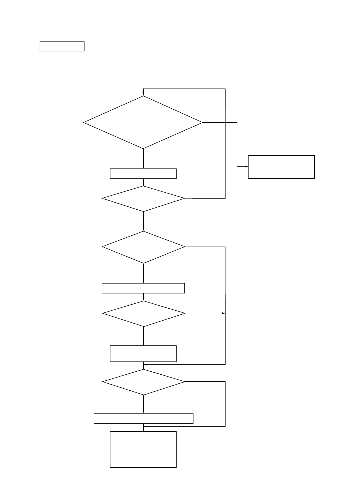
MD SECTION
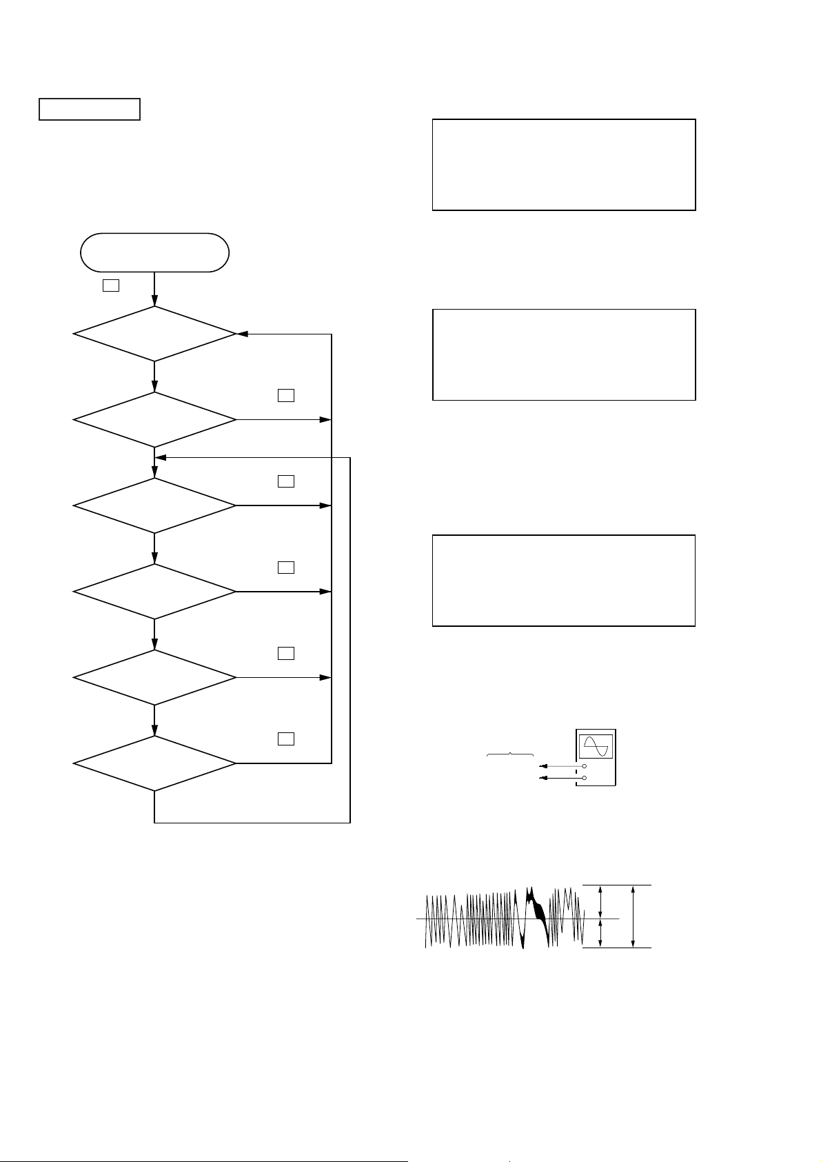
1. PARTS REPLACEMENT AND ADJUSTMENT
• Check and adjust the mechanism deck as follows.
The procedure changes according to the part replaced.
• Laser power check
• Focus bias check
• C PLAY check
• Self-recording/playback check
NG
Parts Replacement and Repair
• Abbreviation
OP : Optical pick-up
OWH :Overwrite head
OK
Check the sled and spindle
mechanisms.
Other causes can be suspected.
Has the OWH been replaced?
NO
Has OP, IC171, IC101, or
IC121 been replaced?
YES
Initial setting of the adjustment value
Has OP or IC171 been replaced?
YES
IOP information recording
(IOP value labeled on OP)
YES
NO
NO
Has IC171 or D101
been replaced?
YES
Temperature compensation offset adjustment
• Laser power adjustment
• Traverse adjustment
• Focus bias adjustment
• Error rate adjustment
• Focus bias check
• Auto gain adjustment
– 21 –
NO
Page 22
2. PRECAUTIONS FOR CHECKING LASER DIODE
EMISSION
T o check the emission of the laser diode during adjustments, nev er
view directly from the top as this may lose your eye-sight.
3. PRECAUTIONS FOR USE OF OPTICAL
PICK-UP (KMS-260A)
As the laser diode in the optical pick-up is easily damaged by static
electricity, solder the laser tap of the fle xible board when using it.
Before disconnecting the connector, desolder first. Before connecting the connector, be careful not to remove the solder. Also
take adequate measures to prevent damage by static electricity.
Handle the flexible board with care as it breaks easily.
pick-up
laser tap
flexible board
Optical pick-up flexible board
4. PRECAUTIONS FOR ADJUSTMENTS
1. When replacing the following parts, perform the adjustments
and checks with ¬ in the order shown in the following table.
D101
BD Board
IC101, IC121
¬G
IC192
1.Temperature
compensation
offset adjustment
2.Laser power
adjustment
3.EF balance
adjustment
4.Focus bias
adjustment
5.Error rate check
Optical
Pick-up
¬
IC171
¬¬GGG
¬G¬¬¬
¬G¬¬G
¬G¬¬G
¬G
4. Use the following tools and measuring devices.
• Check Disc (MD) TDYS-1
(Part No. 4-963-646-01)
• Test Disc (MDW-74/AU-1) (Part No. 8-892-341-41)
• Laser power meter LPM-8001 (Part No. J-2501-046-A)
or MD Laser power meter 8010S (Part No. J-2501-145-A)
• Oscilloscope (Measure after performing CAL of prove)
• Digital voltmeter
• Thermometer
• Jig for checking BD board waveform
(Part No. : J-2501-149-A)
5. When observing several signals on the oscilloscope, etc.,
make sure that VC and ground do not connect inside the oscilloscope.
(VC and ground will become short-circuited)
6. Using the above jig enables the waveform to be checked without the need to solder.
(Refer to Servicing Notes on page 4)
7. As the disc used will affect the adjustment results, make sure
that no dusts nor fingerprints are attached to it.
Laser power meter
When performing laser power checks and adjustment (electrical
adjustment), use of the new MD laser power meter 8010S (Part
No. J-2501-145-A) instead of the conventional laser power meter
is convenient.
It sharply reduces the time and trouble to set the laser power meter
sensor onto the objective lens of optical pick-up.
5. CREATING CONTINUOUSLY-RECORDED DISC
* This disc is used in focus bias adjustment and error rate check.
The following describes how to create a continuous recording
disc.
1. Insert a disc (blank disc) commercially available.
2. Turn the JOG dial and display “CREC MODE”.
3. Press the
Display “CREC (0300)” and start to recording.
4. Complete recording within 5 minutes.
5. Press the [NO,CANCEL] button and stop recording .
6. Press the [MDEJECT] button and remove the disc.
The above has been how to create a continuous recorded data for
the focus bias adjustment/check and MO error rate check.
Note :
• Be careful not to apply vibration during continuous recording.
[YES,ENTER] button again to display “CREC MID”.
6
2. Set the test mode when performing adjustments.
After completing the adjustments, release the test mode.
Perform the adjustments and checks in “group S” of the test
mode.
3. Perform the adjustments to be needed in the order shown.
– 22 –
Page 23
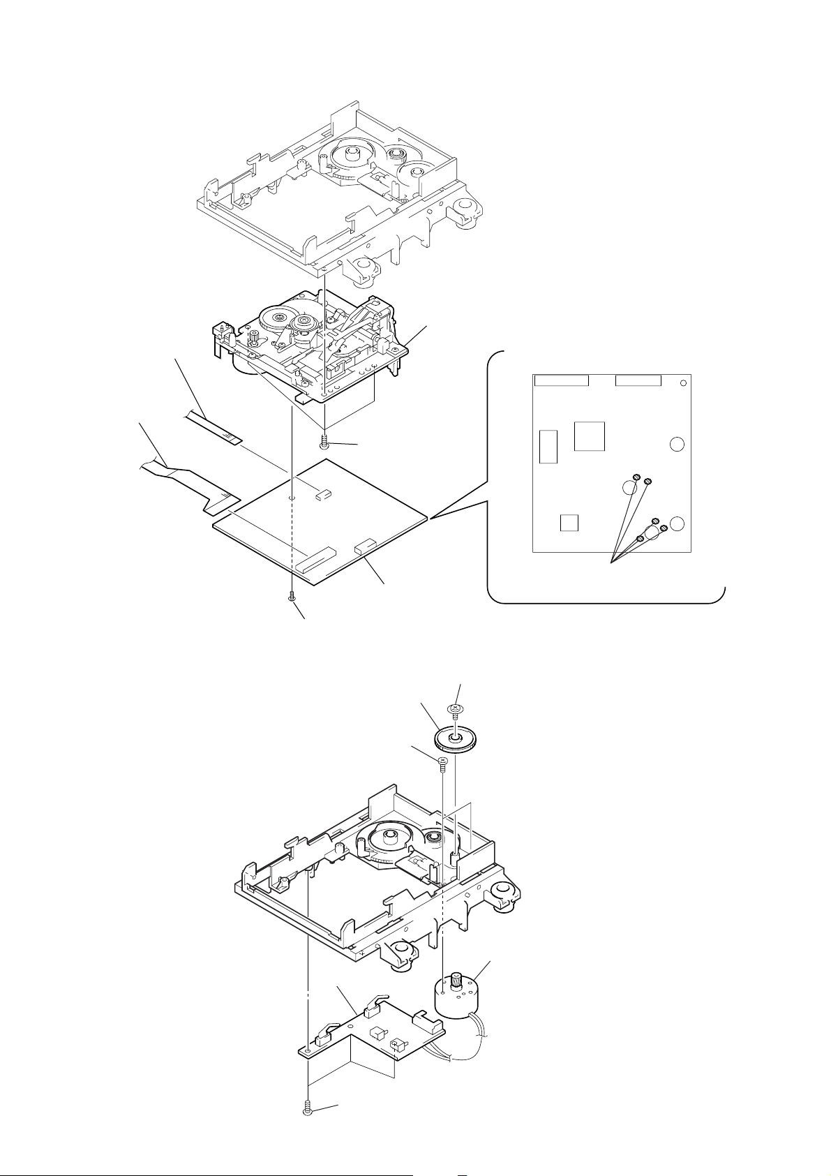
6. CHECK PRIOR TO REPAIRS
r
r
These checks are performed before replacing parts according to
“approximate specifications” to determine the faulty locations. For
details, refer to “Checks Prior to Parts Replacement and Adjustments” (See page 5).
6-1. Laser Power Check
Connection :
laser
power mete
Optical pick-up
objective lens
digital voltmete
BD board
CN110 pin 5 (I +3V)
CN110 pin
4
(IOP)
+
–
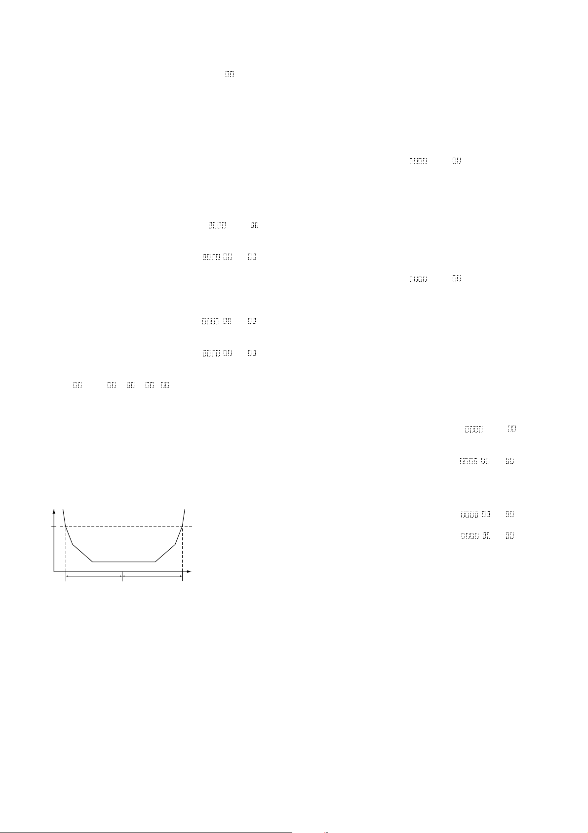
6-2. Focus Bias Check
Change the focus bias and check the focus tolerance amount.
Checking Procedure :
1. Load the test disk (MDW-74/AU-1).
2. Turn the JOG dial to display “CPLAY MODE”.
3. Press the [YES,ENTER] button twice to display “CPLAY
MID”.
4. Press the [NO,CANCEL] button when “C1 = AD = ”
is displayed.
5. Turn the JOG dial to display “FBIAS CHECK”.
6. Press the [YES,ENTER] button to display “ / c = ”.
The first four digits indicate the C1 error rate, the two digits
after [/] indicate ADER, and the 2 digits after [c =] indicate
the focus bias value.
Check that the C1 error is below 50 and ADER is below 2.
7. Press the [YES,ENTER] button to display “ / b = ”.
Check that the C1 error is about 200 and ADER is below 2.
8. Press the [YES,ENTER] button to display “ / a = ”.
Check that the C1 error is about 200 and ADER is below 2.
9. Press the [NO,CANCEL] button, then press the [MDEJECT]
6
button and take out the test disc.
Checking Procedure:
1. Set the laser power meter on the objective lens of the optical
pick-up. (When it cannot be set properly, press the 0 button or ) button to move the optical pick-up)
[]
[]
Connect the digital voltmeter to CN110 pin 5 (I+3V) and
CN110 pin 4 (IOP) on the BD board.
2. Then, turn the JOG dial to display “LDPWR CHECK”.
3. Press the [YES,ENTER] button once to display “LD 0.9 mW
$ ”. Check that the reading of the laser power meter become
0.84 to 0.92 mW.
4. Press the
[YES,ENTER] button once more to display “LD
7.0 mW $ ”. Check that the reading the laser power meter
and digital voltmeter satisfy the specified value.
Specified V alue:
Laser power meter reading : 7.0 ± 0.2 mW
Digital voltmeter reading : Value on the o ptical pick-up label
±10%
(Optical pick-up label)
KMS260A
27X40
B0825
lOP=82.5 mA in this case
lOP (mA) = Digital voltmeter reading (mV)/1 (
Ω
)
5. Press the [NO,CANCEL] button to display “LDPWR CHECK”
and stop the laser emission.
(The [NO,CANCEL] button is effective at all times to stop
the laser emission)
Note 1: After step 4, each time the [YES,ENTER] button is pressed,
the display will be switched “LD 0.7 mW $ ”, “LD 6.2 mW $
”, and “LD WP $ ”. Nothing needs to be performed
here.
6-3. C PLAY Check
MO Error Rate Check
Checking Procedure :
1. Load the test disk (MDW-74/AU-1).
2. Turn the JOG dial to display “CPLAY MODE”.
3. Press the [YES,ENTER] button to display “CPLAY MID”.
4. The display changes to “C1 = AD = ”.
5. If the C1 error rate is below 80, check that ADER is below 2.
6. Press the
the [MDEJECT] button and take out the test disc.
[NO,CANCEL] button to stop playback, then press
6
CD Error Rate Check
Checking Procedure :
1. Load the check disc (MD) TDYS-1.
2. Turn the JOG dial to display “CPLAY MODE”.
3. Press the [YES,ENTER] button twice to display “CPLAY
MID”.
4. The display changes to “C1 = AD = ”.
5. Check that the C1 error rate is below 50.
6. Press the [NO,CANCEL] button to stop playback, then press
the [MDEJECT] button and take out the check disc.
6
6-4. Self-Recording/playback Check
Prepare a continuous recording disc using the unit to be repaired
and check the error rate.
Checking Procedure :
1. Load a recordable disc (blank disc).
2. Turn the JOG dial to display “CREC MODE”.
3. Press the [YES,ENTER] button to display “CREC MID”.
4. When recording starts, lights up “[REC]” and display “CREC
@@@@” (@@@@ is the address).
5. About 1 minute later, press the [NO,CANCEL] button to stop
continuous recording.
6. Turn the JOG dial to display “CPLAY MODE”.
7. Press the [YES,ENTER] button to display “CPLAY MID”.
8. “C1 = AD = ” will be displayed.
9. Check that the C1 error becomes below 80 and the ADER below 2.
10. Press the [NO,CANCEL] button to stop playback, then press
the [MDEJECT] button and take out the disc.
6
– 23 –
Page 24
7. TEMPERATURE COMPENSATION OFFSET
r
r
ADJUSTMENT
Save the temperature data at that time in the non-volatile memory
as 25 ˚C reference data.
Note :
1. Usually, do not perform this adjustment.
2. Perform this adjustment in an ambient temperature of 22 ˚C to 28 ˚C.
Perform it immediately after the power is turned on when the internal
temperature of the unit is the same as the ambient temperature of 22 ˚C
to 28 ˚C.
3. When D101 has been replaced, perform this adjustment after the temperature of this part has become the ambient temperature.
Adjusting Procedure :
1. Turn the JOG dial to display “TEMP ADJUST”.
2. Press the [YES,ENTER] button to select the “TEMP AD-
JUST” mode.
3. “TEMP = ” and the current temperature data will be dis-
played.
4. To save the data, press the [YES,ENTER] button.
When not saving the data, press the [NO,CANCEL] button.
5. When the [YES,ENTER] button is pressed, “TEMP = SAVE”
will be displayed and turned back to “TEMP ADJUST” display then. When the [NO,CANCEL] button is pressed, “TEMP
ADJUST” will be displayed immediately.
Specified Value :
The “TEMP = ” should be within “E0 - EF”, “F0 - FF”, “00 0F”, “10 - 1F” and “20 - 2F”.
8. LASER POWER ADJUSTMENT
7. Then, turn the JOG dial to display “LDPWR CHECK”.
8. Press the [YES,ENTER] button once to display “LD 0.9 mW
$ ”. Check that the reading of the laser power meter become
0.85 to 0.91 mW.
9. Press the [YES,ENTER] button once more to display “LD
7.0 mW $ ”. Check that the reading the laser power meter
and digital voltmeter satisfy the specified value.
Note down the digital voltmeter reading value.
Specified Value:
Laser power meter reading: 7.0 ± 0.2 mW
Digital voltmeter reading : Value on the op tical pick-up label
±10%
(Optical pick-up label)
KMS260A
27X40
B0825
lOP=82.5 mA in this case
lOP (mA) = Digital voltmeter reading (mV)/1 (Ω)
10. Press the
[NO,CANCEL] button to display “LDPWR CHECK”
and stop the laser emission.
(The [NO,CANCEL] button is effective at all times to stop
the laser emission)
Note 1: After step 9, each time the [YES,ENTER] button is pressed, the
display will be switched “LD 0.7 mW $ ”, “LD 6.2 mW $ ”,
and “LD WP $ ”. Nothing needs to be performed
here.
Connection :
laser
power mete
Optical pick-up
objective lens
digital voltmete
BD board
CN110 pin 5 (I +3V)
CN110 pin
4
(IOP)
+
–
Adjusting Procedure :
1. Set the laser power meter on the objective lens of the optical
pick-up. (When it cannot be set properly, press the 0 button
or ) button to move the optical pick-up)
[]
[]
Connect the digital voltmeter to CN110 pin 5 (I+3V) and
CN110 pin 4 (IOP) on the BD board.
2. Turn the JOG dial to display “LDPWR ADJUST”.
(Laser power : For adjustment)
3. Press the
[YES,ENTER] button once to display “LD 0.9 mW
$ ”.
4. Turn the JOG dial so that the reading of the laser power meter
becomes 0.85 to 0.91 mW. Press the [YES,ENTER] button
after setting the range knob of the laser power meter , and sav e
the adjustment results. (“LD SAVE $ ” will be displayed for
a moment)
5. Then “LD 7.0 mW $ ” will be displayed.
6. Turn the JOG dial so that the reading of the laser power meter
becomes 6.9 to 7.1 mW, press the [YES,ENTER] button to
save it.
Note: Do not perform the emission with 7.0 mW more than 15 seconds
continuously.
– 24 –
Page 25
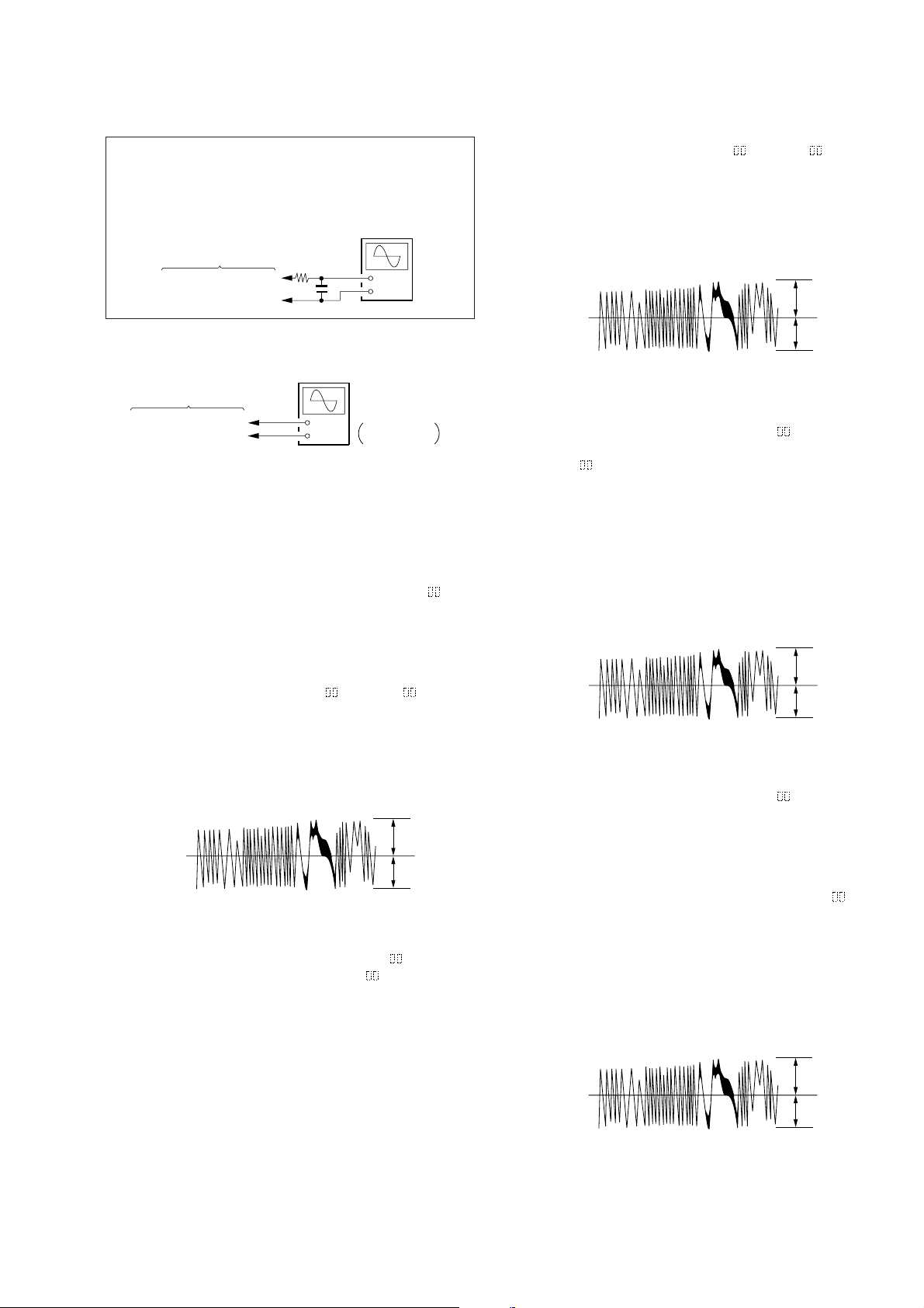
9. EF BALANCE ADJUSTMENT
Note 1:Data will be erased during MO reading if a recorded disc is
used in this adjustment.
Note 2:If the traverse wa veform is not clear , connect the oscilloscope
as shown in the following figure so that it can be seen more
clearly.
BD board
CN110 pin 3 (TEO)
CN110 pin
1
330 k
(VC)
Connection :
oscilloscope
(DC range)
BD board
CN110 pin 3 (TEO)
CN110 pin
1
(VC)
Adjusting Procedure :
1. Connect an oscilloscope to CN110 pin 3 (TEO) and CN110
pin 1 (VC) on the BD board.
2. Load a disc (any available on the market). (Refer to Note 1)
3. Press the ) button to move the optical pick-up outside the
[]
pit.
4. Turn the JOG dial to display “EFBAL ADJUST”.
5. Press the [YES,ENTER] button to display “EFB = MOR”.
(Laser power READ power/Focus servo ON/tracking servo
OFF/spindle (S) servo ON)
6. Turn the JOG dial so that the waveform of the oscilloscope
becomes the specified value.
(When the JOG dial is turned, the
and the waveform changes) In this adjustment, wa veform v aries at intervals of approx. 2%. Adjust the waveform so that
the specified value is satisfied as much as possible.
(Read power traverse adjustment)
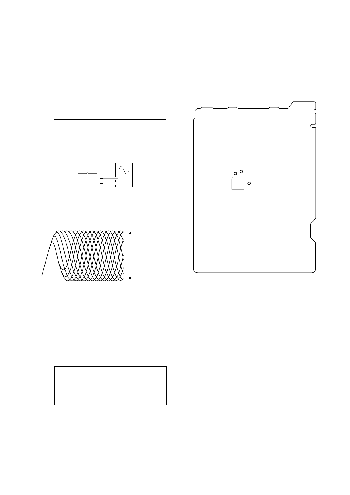
Traverse Wav ef orm
VC
Specification A = B
7. Press the [YES,ENTER] button and save the result of adjustment to the non-volatile memory . (“EFB = SAVE” will
be displayed for a moment. Then “EFB = MO-W” will be
displayed)
oscilloscope
(DC range)
Ω
10 pF
+
–
+
–
V: 0.1 V/div
H: 10 ms/div
of “EFB= ” changes
A
B
8. Turn the JOG dial so that the waveform of the oscilloscope
becomes the specified value.
(When the JOG dial is turned, the
of “EFB- ” changes
and the waveform changes) In this adjustment, wa veform v ar ies at intervals of approx. 2%. Adjust the wa veform so that the
specified value is satisfied as much as possible.
(Write power traverse adjustment)
Traverse Wav ef orm
A
VC
B
Specification A = B
9. Press the [YES,ENTER] button, and save the adjustment results in the non-volatile memory. (“EFB = SAVE” will be
displayed for a moment)
10. “EFB = MO-P” will be displayed.
The optical pick-up moves to the pit area automatically and
servo is imposed.
11. Turn the JOG dial until the waveform of the oscilloscope moves
closer to the specified value.
In this adjustment, waveform varies at intervals of approx. 2%.
Adjust the waveform so that the specified value is satisfied as
much as possible.
Traverse Wav ef orm
A
VC
B
Specification A = B
12. Press the [YES,ENTER] button, and save the adjustment results in the non-volatile memory. (“EFB = SAVE” will be
displayed for a moment)
Next “EFBAL ADJUST” is displayed. The disc stops rotating
automatically.
13. Press the [MDEJECT] button and take out the disc.
6
14. Load the check disc (MD) TDYS-1.
15. Press the [YES,ENTER] button to display “EFB = CD”.
Servo is imposed automatically.
16. Turn the JOG dial so that the waveform of the oscilloscope
moves closer to the specified value.
In this adjustment, waveform varies at intervals of approx. 2%.
Adjust the waveform so that the specified value is satisfied as
much as possible.
– 25 –
Traverse Wav ef orm
A
VC
B
Specification A = B
Page 26
17. Press the [YES,ENTER] button, display “EFB = SAVE”
for a moment and save the adjustment results in the non-volatile memory.
Next “EFBAL ADJUST” will be displayed.
18. Press the [MDEJECT] button and take out the disc.
6
10. FOCUS BIAS ADJUSTMENT
Adjusting Procedure :
1. Load the continuously-recorded disc. (Refer to “5. CREATING CONTINUOUSLY-RECORDED DISC”)
2. Turn the JOG dial to display “CPLAY MODE”.
3. Press the [YES,ENTER] button to display “CPLAY MID”.
4. Press the [NO,CANCEL] button when “C1 = AD = ”
is displayed.
5. Turn the JOG dial to display “FBIAS ADJUST”.
6. Press the [YES,ENTER] button to display “ / a = ”.
The first four digits indicate the C1 error rate, the two digits
after [/] indicate ADER, and the 2 digits after [a =] indicate
the focus bias value.
7. Turn the JOG dial clockwise and find the focus bias value at
which the C1 error rate becomes about 200 (Refer to Note 2).
8. Press the [YES,ENTER] button to display “ / b = ”.
9. Turn the JOG dial counterclockwise and find the focus bias
value at which the C1 error rate becomes about 200.
10. Press the [YES,ENTER] button to display “ / c = ”.
11. Check that the C1 error rate is below 50 and ADER is 00.
Then press the [YES,ENTER] button.
12. If the “( )” in “ - - ( )” is above 20, press the
[YES,ENTER] button.
If below 20, press the [NO,CANCEL] button and repeat the
adjustment from step 2.
13. Press the
Note 1: The relation between the C1 error and focus bias is as shown in
Note 2: As the C1 error rate changes, perform the adjustment using the
C1 error
about
200
[MDEJECT] button and take out the disc.
the following figure. Find points A and B in the follo wing figure
using the above adjustment. The focal point position C is automatically calculated from points A and B.
average vale.
6
11. ERROR RATE CHECK
11-1. CD Error Rate Check
Checking Procedure :
1. Load the check disc (MD) TDYS-1.
2. Turn the JOG dial and display “CPLAY MODE”.
3. Press the [YES,ENTER] button twice and display “CPLAY
MID”.
4. The display changes to “C1 = AD = ”.
5. Check that the C1 error rate is below 20.
6. Press the [NO,CANCEL] button to stop playback, then press
the [MDEJECT] button and take out the check disc.
6
11-2. MO Error Rate Check
Checking Procedure :
1. Load the continuously-recorded disc. (Refer to “5. CREATING CONTINUOUSLY-RECORDED DISC”)
2. Turn the JOG dial to display “CPLAY MODE”.
3. Press the [YES,ENTER] button to display “CPLAY MID”.
4. The display changes to “C1 = AD = ”.
5. If the C1 error rate is below 50, check that ADER is 00.
6. Press the [NO,CANCEL] button to stop playback, then press
the [MDEJECT] button and take out the test disc.
6
12. FOCUS BIAS CHECK
Change the focus bias and check the focus tolerance amount.
Checking Procedure :
1. Load the continuously-recorded disc. (Refer to “5. CREATING CONTINUOUSLY-RECORDED DISC”)
2. Turn the JOG dial to display “CPLAY MODE”.
3. Press the [YES,ENTER] button twice to display “CPLAY
MID”.
4. Press the
is displayed.
5. Turn the JOG dial to display “FBIAS CHECK”.
6. Press the [YES,ENTER] button to display “ / c = ”.
The first four digits indicate the C1 error rate, the two digits
after [/] indicate ADER, and the 2 digits after [c =] indicate
the focus bias value.
Check that the C1 error is below 50 and ADER is below 2.
7. Press the [YES,ENTER] button and display “ / b = ”.
Check that the C1 error is about 200 and ADER is below 2.
8. Press the [YES,ENTER] button and display “ / a = ”.
Check that the C1 error is about 200 and ADER is below 2
9. Press the [NO,CANCEL] button, then press the [MDEJECT]
button and take out the disc.
[NO,CANCEL] button when “C1 = AD = ”
6
B
C A Focus bias value
(F. BIAS)
Note 1: If the C1 error and ADER are above other than the specified
value at points A (step 8. in the abo ve) or B (step 7. in the abov e),
the focus bias adjustment may not have been carried out properly. Adjust perform the beginning again.
– 26 –
Page 27
Adjustment Location:
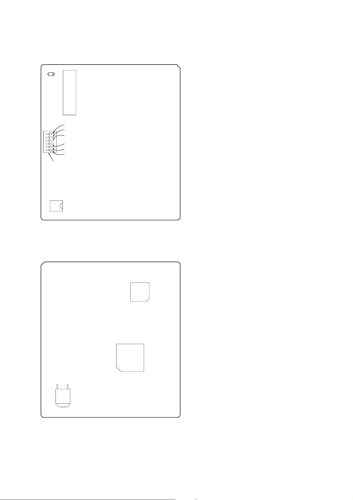
– BD BOARD (Component Side) –
CN101
D101
NOTE
IC171
GND
I+3V
IOP
TEO
RF
VC
CN110
– BD BOARD (Conductor Side) –
IC101
IC121
IC192
Note: It is useful to use the jig for checking the waveform. (Refer to Ser-
vicing Notes on page 4)
– 27 –
Page 28
CD SECTION
Set the CD test mode when performing confirmations.
After completing the confirmation, release the CD test mode.
In the CD test mode, the set works as following sequence.
CD test mode sequence:
Display
88 XX XX XXX
1. Enter the CD test mode
(STOP mode 1)
π
Press the
button.
Press the
button.
Press the
button.
Press the
button.
Press the
button.
Press the
button.
Press the
button.
Note1: ALL SERVO ON mode 1 and TRACKING GAIN UP mode 1:
Note2: TRACKING GAIN UP mode 1,2 is not used in servicing.
(CD)
2. STOP mode 2
[,CD]
fl
[,CD]
fl
[,CD]
fl
[,CD]
fl
[,CD]
fl
[,CD]
fl
LPC ON (Lights up “ALL” indication)
ALL SERVO ON mode 2 and TRACKING GAIN UP mode 2:
LPC OFF (Does not lights up “ALL” indication)
*) LPC: Laser power control
3. FOCUS mode
4. ALL SERVO
ON mode 2
5. TRA CKING
GAIN UP mode 1
6. TRA CKING
GAIN UP mode 2
7. ALL SERVO
ON mode1
Press the π (CD)
button.
Press the π (CD)
button.
Press the π (CD)
button.
Press the π (CD)
button.
Press the π (CD)
button.
1. Entering the CD Test Mode
1. Press the [POWER] button to turn the power ON.
2. Press the [CDOPEN/CLOSE] button to open the disc lid,
and put a disc.
3. Press the [CDOPEN/CLOSE] button to close the disc lid.
4. Press the [POWER] button to standby state.
5. While pressing the both [BASS/TREBLE] and [EDIT] buttons,
press the button [,CD] n [] (CD) n [,CD] n
[] (CD).
π
fl
6. Release the both [BASS/TREBLE] and [EDIT] buttons.
7. After display “CD” for a few seconds, enter the CD test mode
(STOP mode 1), and display as below.
6
6
π
fl
2. STOP Mode 2
1. Press the π (CD) button to enter the STOP mode 2, and
display as below.
[]
Display
88 07 00 3A0
2. Press the + and = button to move the optical pickup to position of the track where signal is recorded.
3. FOCUS Mode (Traverse Confirmation)
1. Press the fl button to enter the FOCUS mode and display
as below. (Focus servo ON. CLV-S, tacking and sled servo
OFF)
[] []
[]
Display
11 07 00 3A0
2. Connect an oscilloscope to TP (TEO) and TP (VC) on the
MAIN board.
Connection:
oscilloscope
(DC range)
MAIN board
TP (TEO)
TP (VC)
3. Confirm that the traverse level of waveform satisfy specified
value as follows.
T ra verse W a vef orm
VC
Specified Value:
traverse level: 160 to 380 mVp-p
Connecting Location: MAIN board (See page 29)
+
–
A = B
A
traverse level:
160 to 380 mVp-p
B
– 28 –
Page 29
4. ALL SERVO ON Mode 1
V
(RF Level and Jitter Confirmation 1)
1. Press the fl button four times to enter the ALL SERVO
ON mode 1 (start playback the disc) and display as below.
(All servo ON. LPC ON)
[]
Display
21 07 00 3A0
ALL
2. Connect an oscilloscope to TP (RFO) and TP (VC) on the
MAIN board.
Connection:
oscilloscope
(DC range)
MAIN board
TP (RFO)
TP (VC)
3. Confirm that the RF level and jitter of waveform satisfy specified values as follows.
+
–
6. Releasing the CD Test Mode
1. Press the π (CD) button to stop rotate the disc.
2. Press the [POWER] button or [RESET] switch (bottom of the
player unit) to release the CD test mode and turn to standby
state.
Connecting Location:
– MAIN BOARD –
(Component Side)
[]
TP (TEO)
TP (VC)
TP (RFO)
IC701
RF signal waveform
VOLT/DIV: 200 m
TIME/DIV: 500 ns
RF level:
1.0 to 1.4 Vp-p
Specified V alues:
RF level: 1.0 to 1.4 Vp-p
jitter : less than 9 nsec
Connecting Location: MAIN board
5. ALL SERVO ON Mode 2
(RF Level and Jitter Confirmation 2)
1. Press the fl button to enter the LPC OFF mode and dis-
play as below. (All servo ON. LPC OFF)
[]
Display
21 07 00 3A0
2. Confirm that the RF level and jitter of waveform satisfy speci-
fied values as follows.
Specified V alues:
RF level: 0.8 to 1.4 Vp-p
jitter : less than 9 nsec
If the RF level and jitter are out of specifide values, measure
again after clean the object lens by an applicator with lens
cleaning liquid.
– 29 –
Page 30
DISPLAY SECITON
r
Dimmer Adjustment
Connection:
digital voltmete
LCD board
TP (DIMMER)
TP (GND)
1. Connect a digital voltmeter to TP (DIMMER) and TP (GND)
on the LCD board.
2. Adjust RV550 so that the value of digital voltmeter becomes
2.83 V.
Specified Value: 2.83 to 2.93 V
Note: Connect the liquid crystal display unit (LCD500) to the LCD board
when performing adjustment.
Adjustment Location:
– LCD BOARD (Component Side) –
+
–
RV550
Dimmer Adjustment
– LCD BOARD (Conductor Side) –
CN553
TP (DIMMER)
TP (GND)
– 30 –
Page 31

6-1. BLOCK DIAGRAM – TUNER Section –
PMC-MD55
SECTION 6
DIAGRAMS
75Ω
FM
EXT ANTENNA
AM
ANTENNA
TU BOARD
TB1
CT2, L4
AM
TRACKING
L1
FM RF
L2
FM OSC
D9
FL1
B.P.F
D7
D8
CT2
CT1, L1
FM
TRACKING
L4
AM
OSC
FM VT
VOLTAGE
L3
AM ANT
CF3
10.7MHz
IF, DET, FM MPX
FM/AM FRONT-END
IC1 (1/2)
12BITS
DIVIDER
FM
IF-IN
7
AM
IF-IN
6
IF
BUFFER
ST-IND
IF-OUT
17 14 1318
FM RF-IN
2
FM RF OUT
24
CT1
FM OSC
21
L2
AM RF-IN
22
AM OSC
20
FM
MIX
FM
OSC
AM
MIX
AM
OSC
MIX-OUT
OSC-OUT
4
FM-IN
12
19
AM-IN
11
PD
16
LP-IN
17
CF1
AM IF
T1
PHASE DETECTOR
CHARGE PUMP
FM
IF AMP
Q14
MUTING
Q7
CF4
PLL, LOW-PASS FILTER
IC2
1/2
SWALLOW
COUNTER
1/16, 1/17
CF2
PROGRAMMABLE
4BIT
10
FM
DET
AM
DET
MO-ST
MONO/ST
SWITCH
Q2 (1/2)
QUAD
AM/FM
BUFFER
BAND
SWITCH
Q2 (2/2)
BAND
DET-OUT
16
IC1 (2/2)
HIGH
FREQUENCY CUT
Q1
15
MPX-IN
R-CH
DIVIDE
DECODE
VCO
MUTE
L-OUT
R-OUT
12
11
MUTING
CN1
12
RA-LCH
R-CH
Q5
A
(Page 40)
REFERENCE
DIVIDER
18
LP-OUT
X IN
19
X1
75kHz
05
X OUT
20
DATA SHIFT
REGISTER
LATCH
CCB/IF
CE
RD
1 2 3 4
ST-IND
8
MO/ST
13
IF-IN
10
MUTING
Q3
BAND
7
CK
CD
COUNT
CLK
DATA
CE
VT
MUTE
DRIVE
Q6
7
MUTE
6
COUNT
5
CLK
3
DATA
2
CE
1
VT
B
C
D
E
F
G
(Page 43)
(Page 43)
(Page 43)
(Page 43)
(Page 43)
(Page 43)
• SIGNAL PATH
: FM
: AM
R-CH : Same as L-CH.
– 31 –
– 32 –
– 33 –
Page 32

PMC-MD55
6-2. BLOCK DIAGRAM – MD Section –
BD BOARD (1/2)
CN104
1
HR901
(OVER WRITE HEAD)
OPTICAL PICK-UP BLOCK
HF MODULE
05
(KMS-260A)
F
C B
I J
D
E
LASER DIODE
2-AXIS
DEVICE
FCS+
(FOCUS)
(TRACKING)
FCS–
TRK+
TRK–
MOD
A
DETECTOR
LDPD
I
J
B
A
C
D
E
F
ILCC
PD
FOCUS/TRACKING COIL DRIVE,
SPINDLE/SLED MOTOR DRIVE
(SPINDLE)
CN101 (2/2)
4
3
2
1
8
M101
M102
(SLED)
CN101 (1/2)
16
12
13
14
18
19
20
17
9
6
IC152
MM
M
AUTOMATIC
POWER CONTROL
Q162, 163
LASER ON
SWITCH
Q101
OUT4F
6
OUT4R
8
OUT2F
27
OUT2R
25
OUT1F
21
23
OUT1R
OUT3F
12
10
OUT3R
16
PSB
IN4R
IN4F
IN2F
IN2R
IN1F
IN1R
IN3F
IN3R
CN102
DIGITAL SIGNAL PROCESSOR,
EFM/ACIRC ENCODER/DECODER,
SHOCK PROOF MEMORY CONTROLLER,
ATRAC ENCODER/DECODER
OVER WRITE
HEAD DRIVE
IC181, Q181, 182
SCTX
48 47
MORFI
MORFO
I
1
J
2
A
4
B
5
I-V
C
AMP
6
D
7
E
8
I-V
F
AMP
9
APC
11
PD
10
SPFD
3
SPRD
4
29
30
19
18
14
15
RF AMP
LD/PD
AMP
RFO
46 40
B.P.F.
3T
TEMP
WBL
AT
AMP
ABCD
AMP
APCREF
12
83 13 67 65 66 75 74 63 64
XRST
APCREF
SFDR
92
SRDR
91
FFDR
88
FRDR
89
TFDR
86
TRDR
85
ADFM
B.P.F.
COMMAND
SERIAL/PARALLEL
CONVERTER,
DECODER
SWDT
10
AUTOMATIC
POWER
CONTROL
DIGITAL SERVO
SIGNAL
PROCESS
PWM GENERATOR
DIGITAL SERVO
SIGNAL PROCESSOR
FOCUS/TRACKING ERROR AMP
FOCUS
ERROR AMP
TRACKING
ERROR AMP
SCLK
XLAT
181716
RECP
IC121 (2/2)
AGCI
WBL
PEAK &
BOTTOM
ADIN
3029
EQ
CONVERTER
AUX1
FROM CPU
INTERFACE
SEQUENCER
IC121 (1/2)
RF AMP,
IC101
RF AGC
& EQ
EQ
AUX
PEAK
BOTM
ADFG
ABCD
3T
WBL
F0CNT
V-I
FE
TE
SE
ABCD
ANALOG MUX
A/D CONVERTER
AUTO
RF
TE
SE
PEAK
FE
XLRF
CKRF
DTRF
38
33
37
36
32
35
34
26
28
20
BOTM
80
81
82
EEPROM
IC171
100
60
59
62
FILTER
61
53
54
57
78
79
XLAT
SCLK
SWDT
HF MODULE
SWITCH
IC103, Q102 – 104
EFMO
FILI
PCO
PLL
CLTV
FILO
SENS
LDOUT
RIN
VREF
OUT1
2
2
INTERFACE
SRDT
SENS
SRDT
6
CN601
(1/2)
ATRAC
CPU
ENCODER/DECODER
SWDT
SCLK
XLAT
SCLK
SWDT
VOLTAGE SWITCH
ASYO
ASYI
COMPA-
RFI
RATOR
ADFG
DEMODULATOR/
DECODER
F0CNT
CN103
(2/5)
ADIP
EFM/ACIRC
SHOCK PROOF
ENCODER/DECODER
MEMORY CONTROLLER
SUBCODE
PROCESSOR
SPINDLE
SERVO
SPFD
SPRD
DQSY
SQSY
XINT
XT
94 93
CN602
(1/4)
CN602
(2/4)
9
15
4
26
17
7
14
10
LDON
75
81
DIG-RST
80
WR-PWR
86
MOD
LOADING
MOTOR DRIVE
IC602
15
12 11 14 9 8 5 6 7 1 2 3 4
3523 7 1 15 18 10 12 20 2 8 19
16
15 12
89 32 69 67 90 77 33 41 4268
XINT
SCTX
SQSY
DQSY
LDIN
95 94
4 5
FIN
OUT2
7 1
CN605
(1/2)
1
1
M
M103
(LOADING)
SW BOARD (1/2)
CN103
(3/5)
SDA
SCL
21
22
6 53
SAMPLING
RATE
CONVERTER
DIGITAL
AUDIO
INTERFACE
CLOCK
GENERATOR
INTERNAL BUS
MONITOR
CONTROL
MNT0
FOK
42216523 9 6 14 1221 19 1 17
FOK
XLATCH
REFERENCE
Q611
IC121 (1/2)
ADDT
25
DATAI
22
XBCKI
24
LRCKI
23
DIN0
19
DIN1
20
DOUT
21
DADT
26
XBCK
28
LRCK
27
FS256
29
MNT1
MNT2
MNT3
SLOCK
XBUSY
SHOCK
CN103
(1/5)
SHOCK
MD MECHANISM CONTROLLER
MNT3 (SLOCK)
MNT2 (XBUSY)
B+
(D +5V)
32.768kHz
CN602
(3/4)
3
2
X601
12MHz
X602
IC601
39
28
27
25
24
525
MD B+
(+3.3V)
OSCI
OSCO
XOE
XWE
XRAS
XCAS
LD-LOW
XIN
XOUT
XIN-T
XOUT-T
SDA
SCL
+3.3V
3
REG
IC192
16
17
D0 – D3A00 – A09
49, 48, 50, 51
34 – 31, 36 – 40, 45
43
47
46
44
DA-RST
PACK-OUT
LIMIT-IN
REFLECT
PROTECT
SYS-RST
PDOWN
RXD (UART)
TXD (UART)
1
DIVIDER
IC123
D-RAM
IC124
1, 2, 18, 19
DQ1 – DQ4
A0 – A9
6 – 9, 11 – 15, 5
XOE
16
XWE
3
XRAS
4
XCAS
17
EMP
70
83
RECP
37
8
PBP
38
96
98
97
STB
36
20
13
57
58
RTS
59
CTS
60
CN605
(2/2)
CN602
(4/4)
13
9
8
14
10
12
1
21
3
19
5
17
7
15
15 7
3
5
7
8
13 11
11 13
CN601
3
5
7
CN103
(4/4)
16
CN601
(2/2)
DG BOARD
B+
(+5V)
12
15
11
10
S102
-1
-2
RESET
SWITCH
Q604
CONVERTER
DOUT
DIN
BCK
LRCK
SW BOARD (2/2)
(REC POSITION)
(PACK OUT)
(PLAY POSITION)
S602
S601
S604
SERIAL
INTERFACE
BD BOARD (2/2)
S101
(LIMIT IN)
S102-1
(REFLECT RATE DETECT)
S102-2
(PROTECT DETECT)
D/A, A/D
IC603
CONVERTER
CONVERTER
(+3.3V)
R-CH
R-CH
Q
CN603
2
D-IN
(Page 39)
H
CN604
(1/2)
8
DA-LCH
3
AD-LCH
12
13
5
1
2
I
J
(Page 40)
(Page 42)
LEVEL
SHIFT
IC604
VOUTL
D/A
A/D
PDADPDDADEMO
7818
VOUTR
VINL
VINR
SYSCK
MD PLAY/REC
1
CLK
7
6
512FS OSC
22.5792MHz
19
20
6
3
9
SWITCH
Q620
D FLIP–
FLOP
IC606
IC605
X603
• SIGNAL PATH
: MD PLAY
: MD REC (ANALOG)
: MD REC (DIGITAL)
R-CH : Same as L-CH.
MAIN BOARD (1/5)
REC-H
18
MD-H
17
MD-RST
19
MD-PDOWN
22
MD-STXD
70
MD-SRXD
69
MD-SCTS
20
MD-SRTS
21
SYSTEM
CONTROLLER
IC405(1/4)
CN405
(1/3)
12
13
21
26
22
23
24
25
B+
SWITCH
Q603
B+
SWITCH
Q617
B+
SWITCH
Q612
Q610
(BU +3.3V)
B+
Q616
B+
(+5V)
B+
B+
B+
(AU +3.3V)
B+
(D +5V)
CN604
(2/2)
21
26
22
23
24
25
– 34 –
– 35 –
– 36 –
Page 33

6-3. BLOCK DIAGRAM – CD Section –
PMC-MD55
OPTICAL PICK-UP
BLOCK
(KSS-213C)
+
–
–
+
–
+
+
–
+
–
–
+
LD
PD
T+
(TRACKING)
T-
F+
(FOCUS)
F-
M1001
M
(SLED)
CN1001
M1002
(SPINDLE)
S1001
(LIMIT)
M
CD MOTOR BOARD
05
SL+
SL–
(1/2)
MAIN BOARD (2/5)
DOUT
RF AMP, FOCUS/TRACKING SERVO
CN701
1
5
6
7
4
3
8
10
12
14
15
13
16
CN702(1/2)
4
4
2
2
OUT4+
15
OUT4–
16
MUTING
VC
AUTOMATIC
POWER
CONTROL
Q701
TRACKING/FOCUS COIL DRIVE,
SLED MOTOR DRIVE
T+
17
T–
18
F+
26
F–
27
SL+
11
SL–
12
MUTE DRIVE
SPINDLE MOTOR
DRIVE
IC1001
IN4
DRIVE
MUTE4
26
Q1001
IC703
LEVEL
LEVEL
LEVEL
27
46
36
37
39
38
34
35
B+
VC
PD1
PD2
E
F
LD
PD
SHIFT
SHIFT
SHIFT
APC
MUTE
MOTOR
CONTROL
Q1002-1005
TIN
FIN
SLIN
B+
SWITCH
Q1006
19
25
10
7
IC701
RF AMP
FE AMP
TRACKING PHASE
COMPENSATION
TA O
12
1 2
Q1007
ILL DATA
REGISTER
INPUT SHIFT,
REGISTER
ADRESS
DECODER
OUTPUT
DECODER
BUFFER
IC1002
IIL
TTL
TTL
IIL
FOCUS PHASE
COMPENSATION
FE O
5 15 32
CN1001
(2/2)
RFO
31
FOK
25
C.OUT
22
SENS1
23
SENS2
24
DATA
20
XLT
19
CLK
18
XRST
21
RF-H
SL O
HIGH SPEED SWITCH
Q705
CN702
(2/2)
5
5
1
1
8
8
77
3
3
99
35
18
11
10
12
13
14
79
B+
(UNREG +8V)
RF
FOK
CNIN
SEIN
DATO
XLTO
CLKO
XRST
CLV
SERVO
XLON
17
EFM
DEMO.
DIGITAL
CLV
MDP
21
D/A
I/F
SUB CODE
PROCESSOR
CPU
I/F
SPOA
15
53
BCK
43
PCMD
41
LRCK
39
EMPH
54
CD O/C BOARD
CD LID CLOSE
DETECT
Q762
(MOTOR)
BCKI
44
PCMDI
42
LRCKI
40
EMPHI
55
M703
CD LID
OPEN/CLOSE
B+
MOTOR
B+ SWITCH
Q764
Q765
DIGITAL SIGNAL PROCESSOR,
CLV SERVO, D/A CONVERTER
IC702
PWM
SERIAL
I/F
PWM
CD LID OPEN/CLOSE MOTOR
DRIVE
IC711
M–
1
M
M+
7
VREF
6
S762
CD LID CLOSE
DETECT
S761
CD LID OPEN
DETECT
B+
(+3.3V)
D704
OP
DRIVE
CL
MOTOR
CONTROL
Q763
MOTOR
CONTROL
Q766
REGULATOR CONTROL
AOUT1
AOUT2
SYSM
SCOR
SENS
SQSO
SQCK
XLAT
CLOK
DATA
XTAI
XTAO
5
4
+3.3V
REGULATOR
Q703
CD POWER
Q702
65
76
62
57
6
5
4
8
9
7
70
71
CN711
7
5
44
1
3
66
R-CH
X701
33.8688MHz
CN404
7
5
1
3
B+
(CD +6V)
B+
(CD6V)
CD-MUTE
82
CD-SCOR
78
CD-SENSE1
77
CD-SQSO
79
81
CD-SQCK
75
CD-XLAT
74
CD-CLK
76
CD-DATA
83
CD-FOK
91
CD-XRST
84
CD-SENSE2
68
HI-SPEED
10
CD-TURN
12
CD-OPEN
13
CD-CLOSE
93
SPEED-L
48
CD-DOOR
34
CD-12HISP
32
R-CH : Same as L-CH.
SYSTEM
CONTROLLER
IC405(2/4)
CD-POWER
CD-SHORT
P-CON43EXTAL42XTAL
80
100
SELECT
SELECT-GND
TU-SFT
X401
8MHz
• SIGNAL PATH
CD L-CH
TX
TEX
P-CON
B+(BU3.3V)
51
44
87
86
39
LEVEL
SHIFT
Q406
M
CN704
(Page 41)
K
(Page 41)
L
X402
32.768kHz
(Page 44)
2
D-OUT
H
(Page 36)
: CD PLAY
– 37 –
– 38 –
: MD REC (DIGITAL)
– 39 –
Page 34

PMC-MD55
6-4. BLOCK DIAGRAM – FUNCTION SELECT/PANEL Section –
(Page 33)
J303
LINE IN
RA-LCH
A
LINE IN BOARD
(Page 36)
R-CH
MAIN BOARD (3/5)
CN408
(1/2)
5
CN305
I
DA L-CH
CN301
3
2
LINE IN
MUTE
Q104
DRIVE
Q305
LINE IN LEVEL
CD L-CH
CONTROL
Q105
LINE IN LEVEL
CONTROL DRIVE
Q306
CN405(2/2)
8
(Page 38)
(Page 38 )
R-CH
LINE IN MUTE
K
L
MD
MUTE
Q102
RADIO
3
LINE
7
R-CH
IN
IN
MD MUTE
DRIVE
Q304
TUNER/LINE IN
SELECT
IC301
SW1
2
CD
MUTE
Q101
OUT
CD MUTE
DRIVE
Q303
5
BUFFER
Q103 (1/2)
R-CH R-CH
BUFFER
Q103 (2/2)
R-CH
TUNER/LINE IN
MUTE
Q106
LOW-PASS
FILTER
IC302
5 7
TUNER/LINE IN
MUTE
DRIVE
Q308
TUNER/LINE IN
MUTE SWITCH
Q307
2
RADIO/LINE
AU-CLK
AU-DATA
CN405
(1/2)
3
CN302
(1/3)
1
95
94
66
5
AD-LCH
J
(Page 36)
AU/JACK BOARD (1/4)
CN307
(1/2)
1
5
IN2
9
L-CH
R-CH
VOL
0dB/6dB
DIGITAL
CONTROL
SCK
SW (TOP) BOARD
D552
BAND
RADIO
DBC
18 2019
SI
D551
BASS TREBLE
L-CH
R-CH
CD
D550
MD
DINAMIC
BASS
ELECTRICAL
VOLUME
IC351
FILTER
PL550
CD DISC
ILLUMINATION
OUT2
N
(Page 43)
16
SW (FRONT) BOARD
HIGH SPEED
05
D555
LED
DRIVE
Q555
D554
SELECT
LED
DRIVE
Q554
D553
PRESET/AMS
LED
DRIVE
Q553
S572-580
S557-564
S565-571
MD MUTE
SWITCH
Q302
REMOTE
CONTROL
RECEIVER
IC550
S556
(JOG DIAL)
CD MUTE
SWITCH
Q301
CN551
22
111011
4
7
9
12
5
1
10
12
4
7
9
5
1
CN407
CD
99
MD
1
58
LINE-LEVEL
LINE
57
KEY1
62
KEY2
61
KEY3
60
RMC
85
JOG-A
49
JOG-B
50
LED-PRESET/AMS
55
LED-SELECT
56
HI-LED
33
SYSTEM
CONTROLLER
IC405 (3/4)
LCD-DATA
46 47 25 26
LED-RADIO
LCD-CLK
LED-CD
LED-MD
KEY4
D/LCON
LCD-RST
BL-CONT
LCD-CE
LCD-AO
CN409
(1/2)
28
29
27
59
23
24
96
CN406(2/3)
CN550 (2/2)
9
7
5
5
PILOT LAMP
DRIVE
Q405
PILOT LAMP
DRIVE
Q410
CN406
(1/3)
CN552
(3/3)
3
CN409 (2/2)
Q404
Q411
BU +3.3V
CN401
CN302
(2/3)
P
2
7
(Page 44)
LIQUID
LED
DRIVE
Q550
B/L
CONTROL
Q407
VDD
V5
VR
14
9
6
8
CN553
(2/2)
DIMMER
RV550
CN550
7
8
6
1
7
8
6
1
(1/2)
Q552
LED
DRIVE
LED
DRIVE
Q551
S550-555,
S579
LAMP BOARD
1
7
6
4
5
LCD BOARD
CN552
(2/3)
1
7
6
4
5
CN553
(1/2)
21
1
3
5
4
DATA
(LCD BACK LIGHT)
RST
AO
CE
CLK
PL553-555
CRYSTAL
DISPLY
LCD500
• SIGNAL PATH
: TUNER
: CD
: MD PLAY
: MD REC (ANALOG)
R-CH : Same as L-CH.
AU/JACK BOARD (2/4)
CN306
1
7
CN307
(2/2)
DIMMER
Q357,358
UNREG +8V
O
(Page 44)
– 40 –
– 41 –
– 42 –
Page 35

6-5. BLOCK DIAGRAM – POWER AMP/POWER SUPPLY Section –
AU/JACK BOARD (3/4)
(Page 42)
N
MEGABASS
SWITCH
R-CH
D353
MEGABASS
Q151
ON/OFF
Q360
LINE
AMP
IC352
3 1
SPEAKER
MUTE
Q152
MEGABASS
CONTROL
Q362, 363
D358
R-CH
MEGABASS
IC354,
Q352, 361
D359
HEADPHONE
AMP
IC353
6 3
HEADPHONE
MUTE
Q154
R-CH
J301
SIGNAL OUTPUT
(TO SPEAKER(L) UNIT)
L
R-CH R-CH
R
CN304
(1/2)
11
CN303
(1/2)
J391
SIGNAL INPUT
(TO PLAYER UNIT)
POWER AMP (A)
L
R
R-CH
BOARD
J301
JACK OUT
JACK IN
MAIN BOARD (4/5)
(Page 45)
Q
J302
SIGNAL OUTPUT
(WOOFER)
MUTE
DRIVE
Q351
D364
(TO SUPER WOOFER UNIT)
PMC-MD55
POWER AMP (C) BOARD
CN392
D901
RECT
1
2
J392
SPEAKER
OUTPUT
R-CH
IMPEDANCE
USE4Ω
POWER AMP (D)
SP391
L-CH
1
2
BOARD
T901
POWER
TRNSFORMER
SPEAKER(R) UNIT
SP392
(R-CH)
STANDBY
+OUT2
–OUT2
+OUT1
–OUT1
9
11
14
12
CN394
2
CN393
44
CN391
1
AUMUTE
2
PA-STBY
4
UNREG 12V
POWER
IN2
4
AMP
SIGNAL MUTE
56
STANDBY
SWITCH
Q391, 392
POWER AMP (B) BOARD
POWER BOARD
CN901
4
UNREG 12V
2
PA-STBY
1
AUMUTE
(Page 33)
(Page 33)
(Page 33)
(Page 33)
(Page 33)
(Page 33)
B+
(AU +8V)
AC
CHECK
Q412
+8V
REGULATOR
Q354
POWER
STANDBY
Q353
8
8
BU +3.3V
REGULATOR
3 2
IC402
B+
SWITCH
Q401
9
9
B+
(MD +5V)
(CD +6V)
B+
SWITCH
Q355
Q356
CN307(2/2)
10
10
(COM+5V)
RESET
SIGNAL
1 2
GENERATOR
IC404
B+
(+3.3V)
B+
RST
97
98
45
40
B+
SWITCH
Q359
CN302 (3/3)
S401
RESET
B+
(HEADPHONE AMP)
CN304 (2/2)
647
CN303 (2/2)
CN402
1
G
B+
(AU +3.3V)
2
F
3
E
5
D
6
C
7
B
B+
(+8V)
647
+3.3V
REGULATOR
IC403
B+
SWITCH
Q413
MAIN BOARD (5/5)
M/B
11
R-CE
67
R-DATA
66
R-CLK
65
R-COUNT
64
R-MUTE
63
SYSTEM
CONTROLLER
RADIO POWER
31
ACCHK
IC405 (4/4)
3
B+
(AU +8V)
PA-STANDBY
A MUTE
HP-SW
B+
D401
CN310
(1/2)
2
AUMUTE
3
UNREG 10V
4
PA-STBY
CN310
POWER INPUT
(TO SPEKER(L) UNIT)
+6V
REGULATOR
Q402
REGULATOR
SWITCHING
Q403,408,409
+5V
REGULATOR
3 1
IC401
HP-SW
P-CON
M
CN401
UNREG 8V
ACCHK
(Page 38)
CN406
(3/3)
BU +3.3V
AU/JACK BOARD (4/4)
CN308
3
3
1
1
UNREG 8V
3
BU +3.3V
P
(Page 42)
UNREG 10V
CN902
POWER OUTPUT
(TO PLAYER UNIT)
CN310
(2/2)
(Page 42)
O
PA-STBY
CN902
2
3
4
8
8
9
9
5
5
UNREG 10V
UNREG 8V
ACCHK
D902
RECT
D905-908
RECT
D903
D903,904
RECT
D904
CN903
AC IN
1
2
• SIGNAL PATH
: FM
R-CH : Same as L-CH.
05
– 43 – – 44 –
Page 36

PMC-MD55
6-6. BLOCK DIAGRAM – SUPER WOOFER Section –
(TO PLAYER UNIT)
Q
(Page 43)
J811
SIGNAL INPUT
(WOOFER)
WOOFER AMP (B) BOARD
FILTER AMP
IC811
5 7 3 1
WOOFER MUTE
Q811, 812
PROTECT CONTROL
Q813
W-LED BOARD
D821
LEVEL
D811
CN803
(1/2)
CN825
W-VOLUME
BOARD
CN821
(1/2)
3
3
CN822
1
1
RV821
LEVEL
CN821
(2/2)
4
1
4
1
CN803
(2/2)
WOOFER AMP (A) BOARD
LED
DRIVE
Q818
3
B+
(+18V)
B+
(+10V)
IN+
BIPOLAR
TRANSCONDACTANCE
INPUT STAGE
STANDBY
SWITCH
Q816
D815
POWER
CONTROL
Q815
+10V REGULATOR
Q814
WOOFER
AMP
IC812
MOS GAIN &
LEVEL SHIFTING
STAGE
CN811 CN802
1
1
MOS
OUTPUT
STAGE
STANDBY/
MUTE
D801-804
RECT
109
MUTESTBY
CONTROL
SHORT
CIRCUIT
PROTECTION
MUTEING
Q817
CN812
OUT
14
T801
POWER
TRANSFORMER
2
(SUPER WOOFER)
CN801
SP800
AC IN
B–
(–18V)
3
3
J801
AC OUTLET
MAX 35W
W-POWER BOARD
05
• SIGNAL PATH
: FM
– 45 –
– 46 –
Page 37

• Circuit Bords Location
d
d
– Player Unit –
LAMP board
SW (FRONT) board
LCD board
BD board
SW (TOP) board
SW board
CD O/C board
CD MOTOR board
AU/JACK board
TU board
MAIN board
– Speaker (L) Section –
POWER board
DG board
LINE IN board
POWER AMP (C) boar
POWER AMP (A) boar
POWER AMP (B) board
– 47 –
POWER AMP (D) board
Page 38

– Super Woofer Section –
W-POWER board
WOOFER AMP (A) board
W-LED board
WOOFER AMP (B) board
W-VOLUME board
– 48 –
Page 39

Page 40

6-8. SCHEMATIC DIAGRAM – TUNER Section – • See page 99 for Waveforms. • See page 101 for IC Block Diagrams.
PMC-MD55
(Page 70)
(Page 70)
– 51 –
Note on Schematic Diagram:
• All capacitors are in µF unless otherwise noted. pF: µµF
50 WV or less are not indicated except for electrolytics
and tantalums.
• All resistors are in Ω and 1/
specified.
¢
•
• C : panel designation.
• A : B+ Line.
: internal component.
4
W or less unless otherwise
• H : adjustment for repair.
• Voltages and waveforms are dc with respect to ground
under no-signal (detuned) conditions.
no mark : FM
(): AM
• V oltages are taken with a VOM (Input impedance 10 MΩ).
Voltage variations may be noted due to normal production tolerances.
– 52 –
• Waveforms are taken with a oscilloscope.
Voltage variations may be noted due to normal production tolerances.
• Circled numbers refer to waveforms.
• Signal path.
F : FM
f : AM
Page 41

PMC-MD55
6-9. SCHEMATIC DIAGRAM – BD Section – • See page 99 for Waveforms. • See page 102 for IC Block Diagrams.
(Page 54)
(Page 61)
– 53 –
(Page 56)
– 54 –
(Page 61)
– 55 –
(Page 61)
Note on Schematic Diagram:
• All capacitors are in µF unless otherwise noted. pF: µµF
50 WV or less are not indicated except for electrolytics
and tantalums.
• All resistors are in Ω and 1/
specified.
Note: The components identified by mark ! or dotted line
with mark ! are critical for safety.
Replace only with part number specified.
4
W or less unless otherwise
• A : B+ Line.
• Voltages and waveforms are dc with respect to ground
under no-signal conditions.
no mark : MD STOP
( ) : MD PLAY
< > : MD REC
• V oltages are taken with a VOM (Input impedance 10 MΩ).
Voltage variations may be noted due to normal production tolerances.
: Impossible to measure
∗
– 56 –
• Waveforms are taken with a oscilloscope.
Voltage variations may be noted due to normal production tolerances.
• Circled numbers refer to waveforms.
• Signal path.
E : MD PLAY
j : MD REC (ANALOG)
q : MD REC (DIGITAL)
Page 42

Page 43

Page 44

6-12. SCHEMATIC DIAGRAM – DG Section – • See page 99 for Waveforms. • See page 104 for IC Block Diagrams.
(Page 55)
PMC-MD55
(Page 55)
(Page 55)
– 61 –
– 62 –
Note on Schematic Diagram:
• All capacitors are in µF unless otherwise noted. pF: µµF
50 WV or less are not indicated except for electrolytics
and tantalums.
• All resistors are in Ω and 1/
specified.
¢
•
• A : B+ Line.
: internal component.
4
W or less unless otherwise
• Voltages and waveforms are dc with respect to ground
under no-signal conditions.
no mark : MD PLAY
( ) : MD STOP
• V oltages are taken with a VOM (Input impedance 10 MΩ).
Voltage variations may be noted due to normal production tolerances.
– 63 –
(Page 70)
(Page 67)
• Waveforms are taken with a oscilloscope.
Voltage variations may be noted due to normal production tolerances.
• Circled numbers refer to waveforms.
• Signal path.
E : MD PLAY
j : MD REC (ANALOG)
q : MD REC (DIGITAL)
Page 45

Page 46

6-14. SCHEMATIC DIAGRAM – MAIN (CD) Section – • See page 100 for Waveforms. • See page 105 for IC Block Diagrams.
PMC-MD55
(Page 70)
(Page 73)
Note on Schematic Diagram:
• All capacitors are in µF unless otherwise noted. pF: µµF
50 WV or less are not indicated except for electrolytics
and tantalums.
• All resistors are in Ω and 1/
specified.
Note: The components identified by mark ! or dotted line
with mark ! are critical for safety.
Replace only with part number specified.
• A : B+ Line.
• Voltages and waveforms are dc with respect to ground
under no-signal conditions.
no mark : CD PLAY
• V oltages are taken with a VOM (Input impedance 10 MΩ).
Voltage variations may be noted due to normal production tolerances.
• Waveforms are taken with a oscilloscope.
Voltage variations may be noted due to normal production tolerances.
• Circled numbers refer to waveforms.
• Signal path.
J : CD
q : MD REC
4
W or less unless otherwise
(Page 79)
(Page 63)
– 67 –
– 68 –
(Page 70)
(Page 72)
– 69 –
Page 47

PMC-MD55
6-15. SCHEMATIC DIAGRAM – MAIN (SYSTEM CONTROL) Section – • See page 100 for Waveforms.
(Page 73)
(Page 73)
(Page
52)
(Page
52)
(Page 73)
(Page
63)
(Page 69)
(Page 78)
(Page 89)
(Page 78)
(Page 69)
(Page 69)
– 70 –
Note on Schematic Diagram:
• All capacitors are in µF unless otherwise noted. pF: µµF
50 WV or less are not indicated except for electrolytics
and tantalums.
• All resistors are in Ω and 1/
specified.
• A : B+ Line.
4
W or less unless otherwise
– 71 –
• Voltages and waveforms are dc with respect to ground
under no-signal (detuned) conditions.
no mark : FM
( ) : CD PLAY
[ ] : MD PLAY
• V oltages are taken with a VOM (Input impedance 10 MΩ).
Voltage variations may be noted due to normal production tolerances.
• Waveforms are taken with a oscilloscope.
Voltage variations may be noted due to normal production tolerances.
– 72 –
(Page 89)
(Page 90)
(Page 84)
• Circled numbers refer to waveforms.
• Signal path.
F : FM
E : MD PLAY
j : MD REC
Page 48

6-16. SCHEMATIC DIAGRAM – MAIN (FUNCTION SELECT) Section –
(Page 69)
(Page 70)
PMC-MD55
(Page 77)
(Page 77)
(Page 72)
(Page 70)
Note on Schematic Diagram:
• All capacitors are in µF unless otherwise noted. pF: µµF
50 WV or less are not indicated except for electrolytics
and tantalums.
• All resistors are in Ω and 1/
specified.
• C : panel designation.
• A : B+ Line.
• Voltages are dc with respect to ground under no-signal
(detuned) conditions.
no mark : FM/LINE IN
( ) : CD PLAY
[ ] : MD PLAY
• V oltages are taken with a VOM (Input impedance 10 MΩ).
Voltage variations may be noted due to normal production tolerances.
• Signal path.
F : FM
J : CD
E : MD PLAY
j : MD REC
4
W or less unless otherwise
– 73 – – 74 –
Page 49

Page 50

6-18. SCHEMATIC DIAGRAM – AUDIO/JACK Section – • See page 107 for IC Block Diagram.
PMC-MD55
(Page 93)
(Page 97)
(Page 72)
(Page 93)
(Page 74)
(Page 72)
(Page 74)
– 77 –
Note on Schematic Diagram:
• All capacitors are in µF unless otherwise noted. pF: µµF
50 WV or less are not indicated except for electrolytics
and tantalums.
• All resistors are in Ω and 1/
specified.
• C : panel designation.
• A : B+ Line.
• Voltages are dc with respect to ground under no-signal
conditions.
4
W or less unless otherwise
– 78 –
no mark : POWER ON
( ) : STANDBY
• V oltages are taken with a VOM (Input impedance 10 MΩ).
Voltage variations may be noted due to normal production tolerances.
• Signal path.
F : FM
Page 51

PMC-MD55
6-19. SCHEMATIC DIAGRAM – CD MOTOR Section – • See page 107 for IC Block Diagram.
(Page 67)
Note on Schematic Diagram:
• All capacitors are in µF unless otherwise noted. pF: µµF
50 WV or less are not indicated except for electrolytics
and tantalums.
• All resistors are in Ω and 1/
specified.
• A : B+ Line.
• Voltages are dc with respect to ground under no-signal
conditions.
no mark : CD PLAY
• V oltages are taken with a VOM (Input impedance 10 MΩ).
Voltage variations may be noted due to normal production tolerances.
4
W or less unless otherwise
– 79 –
– 80 –
Page 52

Page 53

Page 54

6-22. SCHEMATIC DIAGRAM – CD OPEN/CLOSE Section – • See page 107 for IC Block Diagram.
PMC-MD55
(Page 72)
Note on Schematic Diagram:
• All capacitors are in µF unless otherwise noted. pF: µµF
50 WV or less are not indicated except for electrolytics
and tantalums.
• All resistors are in Ω and 1/
specified.
• 5 : fusible resistor.
Note: The components identified by mark ! or dotted line
with mark ! are critical for safety.
Replace only with part number specified.
• A : B+ Line.
• Voltages are dc with respect to ground under no-signal
conditions.
no mark : CD LID CLOSE
( ) : DURING CD LID OPEN
[ ] : DURING CD LID CLOSE
• V oltages are taken with a VOM (Input impedance 10 MΩ).
Voltage variations may be noted due to normal production tolerances.
4
W or less unless otherwise
– 83 –
– 84 –
Page 55

Page 56

6-24. SCHEMATIC DIAGRAM – PANEL Section –
(Page 72)
PMC-MD55
(Page 72)
(Page 72)
Note on Schematic Diagram:
• All capacitors are in µF unless otherwise noted. pF: µµF
50 WV or less are not indicated except for electrolytics
and tantalums.
• All resistors are in Ω and 1/
specified.
• C : panel designation.
• A : B+ Line.
• H : adjustment for repair.
• Voltages are dc with respect to ground under no-signal
conditions.
no mark : LED OFF
( ) : LED ON
• V oltages are taken with a VOM (Input impedance 10 MΩ).
Voltage variations may be noted due to normal production tolerances.
4
W or less unless otherwise
– 89 – – 90 –
Page 57

Page 58

6-26. SCHEMATIC DIAGRAM – POWER AMP/POWER Section –
PMC-MD55
(Page 78)
(Page 78)
Note on Schematic Diagram:
• All capacitors are in µF unless otherwise noted. pF: µµF
50 WV or less are not indicated except for electrolytics
and tantalums.
• All resistors are in Ω and 1/
specified.
• 2 : nonflammable resistor.
• C : panel designation.
Note: The components identified by mark ! or dotted line
with mark ! are critical for safety.
Replace only with part number specified.
• A : B+ Line.
• Voltages are dc with respect to ground under no-signal
conditions.
no mark : POWER ON
( ) : STANDBY
• V oltages are taken with a VOM (Input impedance 10 MΩ).
Voltage variations may be noted due to normal production tolerances.
• Signal path.
F : FM
4
W or less unless otherwise
– 93 –
– 94 –
Page 59

Page 60

6-28. SCHEMATIC DIAGRAM – SUPER WOOFER Section – • See page 107 for IC Block Diagram.
PMC-MD55
Note on Schematic Diagram:
• All capacitors are in µF unless otherwise noted. pF: µµF
50 WV or less are not indicated except for electrolytics
and tantalums.
• All resistors are in Ω and 1/
specified.
• C : panel designation.
Note: The components identified by mark ! or dotted line
with mark ! are critical for safety.
Replace only with part number specified.
• A : B+ Line.
• B : B– Line.
• Voltages are dc with respect to ground under no-signal
conditions.
no mark : SIGNAL IN (POWER ON)
( ) : STANDBY
• V oltages are taken with a VOM (Input impedance 10 MΩ).
Voltage variations may be noted due to normal production tolerances.
• Signal path.
F : FM
4
W or less unless otherwise
(Page 78)
– 97 –
– 98 –
Page 61

• Waveforms
240 ns
4.3 Vp-p
– TU BOARD –
1 IC1 0 (QUAD)
50 mV/DIV, 50 ns/DIV
4 IC121 !§ (OSCI)
1 V/DIV, 10 ns/DIV
– DG BOARD –
1 IC601 @• (XIN)
1 V/DIV, 50 ns/DIV
6 IC605 6
200 mV/DIV, 10 ns/DIV
5 IC702 $£ (BCK) (CD Play Mode)
1 V/DIV, 200 ns/DIV
– MAIN BOARD
(SYSTEM CONTROL Section) –
1 IC405 $™ (XTAL)
1 V/DIV, 50 ns/DIV
140 mVp-p
90 ns
2 IC2 !ª (X IN)
500 mV/DIV, 5 µs/DIV
1.5 Vp-p
75 kHz
– BD BOARD –
1 IC101 1, 2 (I, J) (MD Play Mode)
200 mV/DIV, 500 ns/DIV
45.158 MHz
5 IC121 @¶ (LRCK) (MD Play Mode)
1 V/DIV, 10 µs/DIV
4.3 Vp-p
44.1 kHz
6 C121 @• (XBCK) (MD Play Mode)
1 V/DIV, 100 ns/DIV
4.6 Vp-p
3.4 Vp-p
12 MHz
2 IC601 @∞ (XIN-T)
500 mV/DIV, 10 µs/DIV
32.768 kHz
3 IC603 !¡ (BCK) (MD Play Mode)
1 V/DIV, 100 ns/DIV
2 Vp-p
1.9 Vp-p
3.4 Vp-p
44.6 MHz
– MAIN BOARD (CD Section) –
1 IC701 #¡ (RF O) (CD Play Mode)
500 mV/DIV, 500 ns/DIV
1.2 Vp-p
2 IC701 $¡ (TEO) (CD Play Mode)
50 mV/DIV, 1 µs/DIV
800 mVp-p
4.3 Vp-p
470 ns
6 IC702 $• (XPCK) (CD Play Mode)
2 V/DIV, 100 ns/DIV
7 IC702 &º (XTAI)
500 mV/DIV, 10 ns/DIV
2 Vp-p
8 MHz
2 IC405 *¶ (TX)
1 V/DIV, 20 µs/DIV
2.5 Vp-p
32.768 kHz
570 mVp-p
2 IC101 4 (A) (MD Play Mode)
200 mV/DIV, 500 ns/DIV
450 mVp-p
3 IC101 8, 9 (E, F) (MD Play Mode)
200 mV/DIV, 500 ns/DIV
440 mVp-p
2.8224 MHz
7 IC121 @ª (FS256) (MD Play Mode)
1 V/DIV, 50 ns/DIV
4.8 Vp-p
11.29 MHz
8 IC121 (º (FS4) (MD Play Mode)
1 V/DIV, 2 µs/DIV
4.4 Vp-p
2.8224 MHz
4 IC603 0 (LRCK) (MD Play Mode)
1 V/DIV, 10 µs/DIV
3.7 Vp-p
44.1 kHz
5 IC603 9 (SYSCK)
1 V/DIV, 20 ns/DIV
4.2 Vp-p
Approx.
180 mVp-p
3 IC701 $• (FEO) (CD Play Mode)
50 mV/DIV, 1 µs/DIV
Approx.
120 mVp-p
4 IC702 #ª (LRCK) (CD Play Mode)
1 V/DIV, 10 µs/DIV
4.1 Vp-p
2 Vp-p
33.8688 MHz
176.4 kHz
– 99 –
22.5792 MHz
44.1 kHz
– 100 –
Page 62

• IC Block Diagrams
– TU Board –
IC1 TA2104AN
GND1
FM RF IN
AM LOW OUT
MIX OUT
VCC2
AM IF IN
FM IF IN
GND2
AGC
QUAD
R OUT
L OUT
24
23
22
21
20
19
18
17
16
15
14
13
AM RF IN
FM RF OUT
VCC1
FM OSC
AM OSC
OSC OUT
ST IND
IF OUT
DET OUT
MPX IN
LPF2/MO-ST
LPF1/BAND
1
FM RF
2
3
4
5
6
7
8
9
10
11
MUTE
12
AM IF
FM IF
AGC
FM
MIX
AM
MIX
LEVEL
DET
AM
DET
FM
DET
ST/MO
FM/AM
FM
OSC
AM
OSC
BUFF
BUFF
AF BUFF
VCO
DIVIDE
DECODE
ST
SW
IF REQ
AF
IF BUFF
1/8
IC2 LC72137M-TLM
1
NC
CE
2
DI
3
CCB
4
5
6
7
8
9
10
UNIVERSAL
COUNTER
I/F
PROGRAMMABLE
LATCH
DATA SHIFT REGISTER
CL
DO
B01
B02
B03
I01
I02
12BITS
DIVIDER
UNLOCK
DETECTOR
SWALLOW
COUNTER
1/16,1/17
4BITS
REFERENCE
DIVIDER
PHASE
DETECTOR
CHARGE
PUMP
POWER ON
RESET
1/2
22
NC
21
XOUT
XIN
20
19
AOUT
18
AIN
PD
17
VSS
16
15
VDD
B04
14
FMIN
13
AMIN
12
IFIN
11
– 101 –
Page 63

– BD Board –
IC101 CXA2523AR
MORFO47MORFI46RFO45OPN
48
–
+
RFA1
+
–
AA
BB
CC
DD
EE
FF
–
–
–
–
–
–
–
GRVA
1
2
1
2
EBAL
FBAL
RFA2
OFST
+
–
+
–
HLPT
GRV
1I
2J
CVB
GSW
+
–
+
–
+
–
+
–
+
–
+
–
+
–
IV
3VC
4A
IVR
5B
IVR
6C
IVR
7D
IVR
8E
IVR
9F
IVR
OPO43ADDC42COMPP41COMPO40AGCI39RF AGC38RF37PEAK
44
USROP
EE'
–1
–2
–2
–1
–
–
–
–
+
+
–
–
–
–
+
+
ESW
FF'
+
–
–
+
–
+
BPF3T
BPF22
WBL
WBL
RFA3
PTGR
PBSW
ABCDA
FEA
ATA
EFB TESW
RF AGC EQ
USRC
PEAK
BOTTOM
WBL
ADIP
PTGR
PEAK3T
P-P
PBH
AGC
WBL
3T
EQ
3T
3T WBL
DET
–1
–2
–1
–2
TEMP
DET
EQ
AUX
SW
BPFC
SEA
TEA
VI CONV
TG
TG
36
BOTM
35
ABCD
34
FE
33
AUX
32 ADFG
31 ADAGC
30 ADIN
29 ADFM
28 SE
27 CSLED
26 TE
25 WBLADJ
15
TEMPR
AUXSW
COMMAND
SCRI - PARA
DECODE
17
16
SWDT
SCLK
BGR
VREF
24
23
22
21
20
19
18
XLAT
XSTBY
F0CNT
VREF
EQADJ
3TADJ
VCC
10PD
11APC
12APCREF
+
–
+
–
14
13
GND
TEMPI
– 102 –
Page 64

IC121 CXD2654R
EFMO
DVSS
TEST3
100
99 98 97 96 95 94 93
TEST2
TEST1
FGIN
SPFD
SPRD
SFDR91SRDR90FS489FRDR88FFDR87DVDD86TFDR85TRDR84LDDR83APCREF82DTRF81CKRF80XLRF79F0CNT78ADFG77APC76DCHG
92
MNT0
MNT1
MNT2
MNT3
SWDT
SCLK
XLAT
SRDT
SENS
XRST
SQSY
DQSY
RECP
XINT
OSCI
OSCO
XTSL
DIN0
DIN1
DOUT
SPINDLE
EACH
BLOCK
EACH
BLOCK
DECODER
EACH
BLOCK
SERVO
ADIP
SHOCK RESISTANT
MEMORY CONTROLLER
DIGITAL
AUDIO
I/F
1
2
MONITOR
CONTROL
3
4
5
6
CPU I/F
7
8
9
10
11
SUBCODE
PROCESSOR
12
13
14
15
TX
16
17
18
19
20
21
CLOCK
GENERATOR
GENERATOR
SERVO
DSP
SAMPLING
RATE
CONVERTER
PWM
A/D
CONVERTER
AUTO
SEQUENCER
ENCODER/
EFM/ACIRC
ANALOG
MUX
DECODER
COMP
PLL
75
TE
74
SE
73
AVSS
72
ADRB
71
ADRT
70
AVDD
69
ADIO
68
VC
67
AUX1
66
FE
65
ABCD
64
BOTM
63
PEAK
62
CLTV
61
FILO
60
FILI
59
PCO
58
AVSS
57
RFI
56
BIAS
55
AVDD
54
ASYI
53
ASYO
22
DATAI
LRCKI
XBCKI
ADDT
23
24
25
30
28
29
26
27
LRCK
XBCK
DADT
FS256
DVDD
ATRAC
ENCODER/DECODER
ADDRESS/DATA BUS A00 - A11, D0 - D3
42
41
A1140A0839A0738A0637A0536A0435A1034A0033A0132A0231A03
43
DVSS
XOE
44
45
XCAS
A09
IC152 BH6511FS-E2
CAPA–
CAPA+
IN2R
IN2F
VM2
OUT2F
PGND2
OUT2R
VM12
OUT1R
PGND1
OUT1F
VM1
32 31 30 29 28 27 26 25 24 23 22 21 20 19 18 17
CHARGE
PUMP.
OSC
INTERFACE
INTERFACE
AMP
AMP
AMP
AMP
AMP
PREDRIVEPREDRIVE
PREDRIVEPREDRIVE
AMPAMPAMP
46
XWE
XRAS
IN1F
INTERFACE
INTERFACE
IN1R
V
PSB
52
MVCI
51
D3
50D249D048D147
DD
V
DD
1 2 3 4 5 6 7 8 9 10 11 12 13 14 15 16
VG
GND
IN4R
IN4F
VM4
OUT4F
PGND4
OUT4R
VM34
OUT3R
PGND3
OUT3F
VM3
IN3F
IN3R
– 103 –
PSB
Page 65

– DG Board –
IC603 PCM3003E/T2
VCC2
AGND1
AGND2
VCOM
VOUTR
24 23 22 21 20 19 18 17 16 15 14 13
VOUTL
DEM0
DEM1
MODE CONTROL
INTERFACE
20BIT
DIN
VDD
DGND
POWER
SUPPLY
ANALOG
LOW-PASS
FILTER
ANALOG
LOW-PASS
FILTER
DECIMATION
&
LOW CUT FILTER
DELTA-SIGMA
MODULATOR
(+) (-) (+) (-)
ANALOG
FRONT-END
CIRCUIT
MULTI-LEVEL
DELTA-SIGMA
MODULATOR
D/A
CONVERTER
MULTI-LEVEL
DELTA-SIGMA
MODULATOR
A/D
CONVERTER
REFERENCE
INTERPOLATION
FILTER
OVERFLOWING
INTERPOLATION
FILTER
OVERFLOWING
DECIMATION
LOW CUT FILTER
DELTA-SIGMA
MODULATOR
ANALOG
FRONT-END
CIRCUIT
SERIAL
INTERFACE
&
RESET AND
POWER DOWN
CLOCK
12 3 45
VCC1
VCC1
VINR
VERF1
IC606 TC7WH74FU (TR12R)
CLR
PR
VCC
8
1
CK
7
2
D
Q
6
5
RSQ
QDC
3
4
Q
GND
VERF2
6 7 8 9 10 11 12
VINL
PDAD
PDDA
SYSCK
LRCK
BCK
DOUT
– 104 –
Page 66

– MAIN Board –
FEI
FOFCT
FGD
FLB
FE_O
FE_M
SRCH
TGU
TG2
FSET
TA_M
TA_O
SL_P
SL_M
SL_O
ISET
VCC
VCC
CLK
XLT
DATA
XRST
C. OUT
SENS1
SENS2
FOK
CC2
CC1
CB
CP
RF_I
RF_O
RF_H
RFTC
LD
PD
PD1
F
E
VEE
TEO
LPFI
ATSC
TZC
VC
FZC
TM2
VEEVEE
TM3
TM5
TM4 TM6
VCC VCC
TM7
ISET
TTL
↓
IIL
IIL
↓
TTL
IIL
↓
TTL
IIL DATA REGISTER
INPUT SHIFT REGISTER
ADDRESS DECODER
SENS SELECTOR
OUTPUT DECODER
DFCTO
IFB1-6
BAL1-4
TOG1-4
FS1-4 TG1-2 TM1-7 PS1-4
FOH
FOL
TGH
TGL
BALH
BALL
ATSC
TZC
FZC
FSET
TG2
VEE
VCC
FS1
FS2
FOCUS
PHASE COMPENSATION
DFCT
FS4
TRACKING
PHASE COMPENSATION
TG1
TM1
DFCT
FZC COMP.
VEE
VCC
VCC
TDFCT
TZC COMP.
ATSC
WINDOW
COMP.
E-F BALANCE
WINDOW COMP.
TRK. GAIN
WINDOW
COMP.
FO. BIAS
WINDOW
COMP.
VEE
TGFL
TOG1
TOG2
TOG3
TOG4
BAL1
BAL2
BAL3
BAL4
IFB1
IFB2
IFB3
IFB4
IFB5
IFB6
FE AMP
VEE
E IV AMP
F IV AMP
VCC
APC
VCC
VCC
VEE
VEE
LASER POWER CONTROL
VEE
PD1 IV
AMP
RF
SUMMING
AMP
VCC
VEE
VEE
LEVEL S
VEE
MIRR
VCC
FOK
VCC
INT
LDON
LPCL
LPC
TGFL
MIRR
DFCT2
XDFCT1
CC1
PD2 IV
AMP
1 2 3 4 5 6 7 8 9 10 11 12
24
38
PD2
37
39
40
41
42
43
44
45
46
47
FEO
48
36 35 34 33 32 31 30 29 28 27 26 25
23
22
21
20
19
18
17
16
15
14
13
VCC
VCC
VEE
VEE
IC701 CXA2542AQ
– 105 –
Page 67

IC702 CXD3009Q
60
VSS3
59
EXCK
58
SBSO
57
SCOR
56
WFCK
55
EMPHI
54
EMPH
53
DOUT
GFS
48
XUGF
47 46 45
PCMD
PCMDI
BCK
41
42
43
44
XTSL
C4M
C2PO
50 49
51
52
BCKI
VSS2
VDD2
XPCK
VDD3
SYSM
AVSS
AVDD
AOUT1
AIN1
LOUT1
AVSS
XVDD
XTAI
XTAO
XVSS
AVSS
LOUT2
AIN2
AOUT2
AVDD
AVSS
XRST
VDD0
EFM
DEMODULATOR
61
62
63
64
65
TIMING
LOGIC
PWM
PWM
3RD-ORDER
NOISE
SHAPER
OVER SAMPLING
DIGITAL FILTER
66
67
68
69
70
71
72
73
74
75
76
77
78
79
80
ERROR
CORRECTOR
16K RAM
CPU
INTERFACE
DIGITAL
CUT
SERVO AUTO
SEQUENCER
SERIAL-IN
INTERFACE
D / A
D / A
INTERFACE
INTERFACE
ASYMMETRY
CORRECTOR
DIGITAL
PLL
OSC
CLOCK
GENERATOR
DIGITAL
CLV
40
LRCKI
39
LRCK
38
ASYO
37
ASYI
36
BIAS
35
RF
34
AVDD
33
CLTV
32
AVSS
31
FILI
30
FILO
29
PCO
28
VCTL
27
V16M
26
VCKI
25
VPCO
24
TEST1
23
TEST0
22
PWM1
21
MDP
IC703 BA6998FP-E2
GND
OUT4-B
DRIVE
BUFFER
LEVEL
SHIFT
+
–
OUT1-A
OUT4-AIN4
–
+
4
IN1
RESET
REG-B
28 27 26 25 24
LEVEL
SHIFT
DRIVE
BUFFER
1 2 3 5 6
OUT1-B
1 2
VSS0
IN4'
VREFIN
VCC
VCC
VCC
20 19 18 17 16
VCC
7 8 9
MUTE
23 22 21
REGULATOR VOLTAGE DETECT,
BIAS VOLTAGE DETECT,
THERMAL SHUT DOWN
–
+
REGOUT
IN3'
3
LMUT
RMUT
IN3
OUT3-AOUT3-B
DRIVE
BUFFER
LEVEL
SHIFT
–
+
DRIVER
MUTING
10 11 12 13 14
IN2
IN2'
GND
4
56789
SQCK
SQSO
+
–
LEVEL
SHIFT
DRIVE
BUFFER
OUT2-A
SENS
XLAT
DATA
NC
OUT2-B
CLOCK
15
+
GND
OPOUT
OPIN-B
–
14
XLTO
CLKO
15 16 17
SPOA
12 13
11
10
SEIN
CNIN
DATO
SPOB
XLON
18 19 20
FOK
VDD1
VSS1
– 106 –
Page 68

– AU/JACK Board –
W
IC351 BH3863F-E2
TREBLE
BASS
1
BASS1
TRE1
24
2
SIMOUT1
3
SIMIN1
DINAMIC
BASS
VOL
BIN1
23
FILTER
BOUT1
22
4
IN1
21
OUT1
SI19SCK18DBC
20
DIGITAL
CONTROL
5
6
VCC
FILTER
– CD MOTOR Board –
IC1001 BA6892FP-E2
VCCPRE
IN4
28 27 26 25 24 23 22 21 20 19 18 17 16 15
VCC
1 2 3 4
IN1
BIAS
MUTE4
IN3
CH4
MUTING
–
+
+
–
CH1
MUTING
IN2
MUTE1
–
+
THERMAL
SHUTDOWN
+
–
MUTE3NCPRGND
CH3
MUTING
CH2
MUTING
5
MUTE2
PWGND
PWGND
PVCC
PVCC
6 7 8 9 10 11 12 13 14
TEST
PWGND
PWGND
PREGND
VCCPOW
VCCPO
DRIVER
DRIVER
CH2
OUT2–
OUT3–
CH3
OUT2+
OUT3+
DRIVER
7
GND
OUT4–
DRIVER
CH4
CH1
OUT1–
17
8
OUT4+
OUT1+
CAP
ALCC
16
OUT2
9
IN2
BOUT2
15 14
FILTER
BIN2
VOL
DINAMIC
BASS
0dB/6dB0dB/6dB
10
TREBLE
BASS
11
SIMIN2
SIMOUT2
TRE2
13
12
BASS2
– CD O/C Board –
IC711 BA6289F-E2
GND
OUT2
8 7 6 5
DRIVER
THERMAL
SHUTDOWN
1 2 3 4
VM
OUT1
POWER
SAVE
VREF
VCC
CONTROL
LOGIC
FIN
RIN
– WOOFER AMP (A) Board –
IC812 TDA7296
BIPOLAR
TRANSCONDACTANCE
INPUT STAGE
–
+
IN+
NC
IN+ MUTE
IN–
STBY-GND
– 107 –
MOS GAIN &
LEVEL SHIFTING
STAGE
BOOST-
STRAP
BOOSTSTRAP
+VS
STANDBY/
MUTE
–VS
STBY
THERMAL
SHUTDOWN
MOS
OUTPUT
STAGE
MUTE
SHORT
CIRCUIT
PROTECTION
NC
NC
14 1512 1310 118 96 753 41 2
OUT
+PWVS
–PWVS
Page 69

6-29. IC PIN FUNCTION DESCRIPTION
• BD BOARD IC101 CXA2523AR (RF AMP, FOCUS/TRACKING ERROR AMP)
Pin No. Pin Name I/O Description
1II
2JI
3VCO
4 to 9 A to F I
10 PD I
11 APC O
12 APCREF I
13 GND —
14 TEMPI I
15
16 SWDT I
17 SCLK I
18 XLAT I
19 XSTBY I
20 F0CNT I
21 VREF O
22 EQADJ I
23 3TADJ I
24 VCC —
25 WBLADJ I
26 TE O
27 CSLED I
28 SE O
29 ADFM O
30 ADIN I
31 ADAGC I
32 ADFG O
33 AUX O
34 FE O
35 ABCD O
36 BOTM O
37 PEAK O
38 RF O
39 RFAGC I
40 AGCI I
41 COMPO O
42 COMPP I
43 ADDC I
44 OPO O
45 OPN I
46 RFO O
47 MORFI I
48 MORFO O
TEMPR O
I-V converted RF signal I input from the optical pick-up block detector
I-V converted RF signal J input from the optical pick-up block detector
Middle point voltage (+1.65V) generation output terminal
Signal input from the optical pick-up detector
Light amount monitor input from the optical pick-up block laser diode
Laser amplifier output terminal to the automatic power control circuit
Reference voltage input terminal for setting laser power
Ground terminal
Connected to the temperature sensor
Output terminal for a temperature sensor reference voltage
Writing serial data input from the CXD2654R (IC121)
Serial data transfer clock signal input from the CXD2654R (IC121)
Serial data latch pulse signal input from the CXD2654R (IC121)
Standby signal input terminal “L”: standby (fixed at “H” in this set)
Center frequency control voltage input terminal of internal circuit (BPF22, BPF3T, EQ) input
from the CXD2654R (IC121)
Reference voltage output terminal Not used (open)
Center frequency setting terminal for the internal circuit (EQ)
Center frequency setting terminal for the internal circuit (BPF3T)
Power supply terminal (+3.3V)
Center frequency setting terminal for the internal circuit (BPF22)
Tracking error signal output to the CXD2654R (IC121)
Connected to the external capacitor for low-pass filter of the sled error signal
Sled error signal output to the CXD2654R (IC121)
FM signal output of the ADIP
Receives a ADIP FM signal in AC coupling
Connected to the external capacitor for ADIP AGC
ADIP duplex signal (22.05 kHz ± 1 kHz) output to the CXD2654R (IC121)
Auxiliary signal (I
Focus error signal output to the CXD2654R (IC121)
Light amount signal (ABCD) output to the CXD2654R (IC121)
Light amount signal (RF/ABCD) bottom hold output to the CXD2654R (IC121)
Light amount signal (RF/ABCD) peak hold output to the CXD2654R (IC121)
Playback EFM RF signal output to the CXD2654R (IC121)
Connected to the external capacitor for RF auto gain control circuit
Receives a RF signal in AC coupling
User comparator output terminal Not used (open)
User comparator input terminal Not used (fixed at “L”)
Connected to the external capacitor for cutting the low band of the ADIP amplifier
User operational amplifier output terminal Not used (open)
User operational amplifier inversion input terminal Not used (fixed at “L”)
RF signal output terminal
Receives a MO RF signal in AC coupling
MO RF signal output terminal
3 signal/temperature signal) output to the CXD2654R (IC121)
– 108 –
Page 70

• BD BOARD IC121 CXD2654R
(DIGITAL SIGNAL PROCESSOR, DIGITAL SERVO SIGNAL PROCESSOR, EFM/ACIRC ENCODER/DECODER,
SHOCK PROOF MEMORY CONTROLLER, ATRAC ENCODER/DECODER)
Pin No. Pin Name I/O Description
1 MNT0 (FOK) O
2 MNT1 (SHOCK) O
3 MNT2 (XBUSY) O
4 MNT3 (SLOCK) O
5 SWDT I
6 SCLK I (S)
7 XLAT I (S)
8 SRDT O (3)
9 SENS O (3)
10 XRST
11
12
13 RECP I
14 XINT O Interrupt status output to the MD mechanism controller (IC601)
15 TX I
16 OSCI I System clock signal (512Fs=22.5792 MHz) input terminal
17 OSCO O System clock signal (512Fs=22.5792 MHz) output terminal Not used (open)
18 XTSL I
19 DIN0 I
20
21
22
23
24
25
26
27
28
29 FS256 O
30 DVDD — Power supply terminal (+3.3V) (digital system)
31 to 34
35
36 to 40
41 A11 O
42 DVSS — Ground terminal (digital system)
43 XOE O Output enable signal output to the D-RAM (IC124) “L” active
44 XCAS O Column address strobe signal output to the D-RAM (IC124) “L” active
45 A09 O Address signal output to the D-RAM (IC124)
SQSY O
DQSY O
DIN1 I Digital audio signal input terminal when recording mode (for digital optical input)
DOUT O
DATAI I Serial data input terminal Not used (fixed at “L”)
LRCKI I L/R sampling clock signal (44.1 kHz) input terminal Not used (fixed at “L”)
XBCKI I Bit clock signal (2.8224 MHz) input terminal Not used (fixed at “L”)
ADDT I Recording data input from the A/D, D/A converter (IC603)
DADT O Playback data output to the A/D, D/A converter (IC603)
LRCK O L/R sampling clock signal (44.1 kHz) output to the A/D, D/A converter (IC603)
XBCK O Bit clock signal (2.8224 MHz) output to the A/D, D/A converter (IC603)
A03 to A00 O Address signal output to the D-RAM (IC124)
A10 O
A04 to A08 O Address signal output to the D-RAM (IC124)
Focus OK signal output to the MD mechanism controller (IC601)
“H” is output when focus is on (“L”: NG)
Track jump detection signal output to the MD mechanism controller (IC601)
Busy monitor signal output to the MD mechanism controller (IC601)
Spindle servo lock status monitor signal output to the MD mechanism controller (IC601)
Writing serial data signal input from the MD mechanism controller (IC601)
Serial data transfer clock signal input from the MD mechanism controller (IC601)
Serial data latch pulse signal input from the MD mechanism controller (IC601)
Reading serial data signal output to the MD mechanism controller (IC601)
Internal status (SENSE) output to the MD mechanism controller (IC601)
I (S)
Reset signal input from the MD mechanism controller (IC601) “L”: reset
Subcode Q sync (SCOR) output to the MD mechanism controller (IC601)
“L” is output every 13.3 msec Almost all, “H” is output
Digital In U-bit CD format subcode Q sync (SCOR) output to the MD mechanism controller
(IC601) “L” is output every 13.3 msec Almost all, “H” is output
Laser power selection signal input from the MD mechanism controller (IC601)
“L”: playback mode, “H”: recording mode
Recording data output enable signal input from the MD mechanism controller (IC601)
Writing data transmission timing input (Also serves as the magnetic head on/off output)
Input terminal for the system clock frequency setting
“L”: 45.1584 MHz, “H”: 22.5792 MHz (fixed at “H” in this set)
Digital audio signal input terminal when recording mode (for digital optical input) Not used
Digital audio signal output terminal when playback mode (for digital optical output)
Not used
Clock signal (11.2896 MHz) output terminal Not used (open)
Address signal output to the external D-RAM Not used (open)
Address signal output to the external D-RAM Not used (open)
– 109 –
Page 71

Pin No. Pin Name I/O Description
46 XRAS O Row address strobe signal output to the D-RAM (IC124) “L” active
47 XWE O Write enable signal output to the D-RAM (IC124) “L” active
48 D1 I/O
49 D0 I/O
50 D2 I/O
Two-way data bus with the D-RAM (IC124)
51 D3 I/O
52 MVCI
I (S)
Digital in PLL oscillation input from the external VCO Not used (fixed at “L”)
53 ASYO O Playback EFM full-swing output terminal
54 ASYI I (A) Playback EFM asymmetry comparator voltage input terminal
55 AVDD — Power supply terminal (+3.3V) (analog system)
56 BIAS I (A) Playback EFM asymmetry circuit constant current input terminal
57 RFI I (A) Playback EFM RF signal input from the CXA2523AR (IC101)
58 AVSS — Ground terminal (analog system)
59 PCO O (3) Phase comparison output for master clock of the recording/playback EFM master PLL
60 FILI I (A) Filter input for master clock of the recording/playback master PLL
61 FILO O (A) Filter output for master clock of the recording/playback master PLL
62 CLTV I (A) Internal VCO control voltage input of the recording/playback master PLL
63 PEAK I (A) Light amount signal (RF/ABCD) peak hold input from the CXA2523AR (IC101)
64 BOTM I (A) Light amount signal (RF/ABCD) bottom hold input from the CXA2523AR (IC101)
65 ABCD I (A) Light amount signal (ABCD) input from the CXA2523AR (IC101)
66 FE I (A) Focus error signal input from the CXA2523AR (IC101)
3
67 AUX1 I (A) Auxiliary signal (I
signal/temperature signal) input from the CXA2523AR (IC101)
68 VC I (A) Middle point voltage (+1.65V) input from the CXA2523AR (IC101)
69 ADIO O (A) Monitor output of the A/D converter input signal Not used (open)
70 AVDD — Power supply terminal (+3.3V) (analog system)
71 ADRT I (A) A/D converter operational range upper limit voltage input terminal (fixed at “H” in this set)
72 ADRB I (A) A/D converter operational range lower limit voltage input terminal (fixed at “L” in this set)
73 AVSS — Ground terminal (analog system)
74 SE I (A) Sled error signal input from the CXA2523AR (IC101)
75 TE I (A) Tracking error signal input from the CXA2523AR (IC101)
76 DCHG I (A) Connected to the +3.3V power supply
77 APC I (A) Error signal input for the laser automatic power control Not used (fixed at “H”)
78 ADFG
I (S)
ADIP duplex FM signal (22.05 kHz ± 1 kHz) input from the CXA2523AR (IC101)
79 F0CNT O Filter f0 control signal output to the CXA2523AR (IC101)
80 XLRF O Serial data latch pulse signal output to the CXA2523AR (IC101)
81 CKRF O Serial data transfer clock signal output to the CXA2523AR (IC101)
82 DTRF O Writing serial data output to the CXA2523AR (IC101)
83 APCREF O
Control signal output to the reference voltage generator circuit for the laser automatic power
control
84 LDDR O PWM signal output for the laser automatic power control Not used (open)
85 TRDR O Tracking servo drive PWM signal (–) output to the BH6511FS (IC152)
86 TFDR O Tracking servo drive PWM signal (+) output to the BH6511FS (IC152)
87 DVDD — Power supply terminal (+3.3V) (digital system)
88 FFDR O Focus servo drive PWM signal (+) output to the BH6511FS (IC152)
89 FRDR O Focus servo drive PWM signal (–) output to the BH6511FS (IC152)
90 FS4 O Clock signal (176.4 kHz) output terminal (X’tal system) Not used (open)
– 110 –
Page 72

Pin No. Pin Name I/O Description
91 SRDR O Sled servo drive PWM signal (–) output to the BH6511FS (IC152)
92 SFDR O Sled servo drive PWM signal (+) output to the BH6511FS (IC152)
93 SPRD O Spindle servo drive PWM signal (–) output to the BH6511FS (IC152)
94 SPFD O Spindle servo drive PWM signal (+) output to the BH6511FS (IC152)
95
96
97
98
99 DVSS — Ground terminal (digital system)
100 EFMO O EFM signal output terminal when recording mode
* I (S) stands for schmitt input, I (A) for analog input, O (3) for 3-state output, and O (A) for analog output in the column I/O.
FGIN
TEST1 I
TEST2 I
TEST3 I
I (S)
Input terminal for the test (fixed at “L”)
– 111 –
Page 73

• MAIN BOARD IC405 CXP740096-024Q (SYSTEM CONTROLLER)
Pin No. Pin Name I/O Description
1 MD O Function select signal output for the MD playback signal “L”: MD, “H”: other function
2 RADIO/LINE O
3 AC-CHK I AC power supply detection signal input “L”: AC in
4 to 6 NC
7 RDS-DATA I
8NC
9 RDS-CLK
10 CD-TURN
11 M/B O MEGA BASS on/off control signal output “L”: MEGA BASS on
12 CD-OPEN O CD lid open/close motor (M703) drive signal output “H”: during CD lid open
13 CD-CLOSE O CD lid open/close motor (M703) drive signal output “H”: during CD lid close
14 to 16 NC
17 MD-H O MD play control signal output to the A/D, D/A converter (IC603) “L”: MD playback mode
18 REC-H O MD rec control signal output to the A/D, D/A converter (IC603) “L”: MD recording mode
19 MD-RST O
20 MD-SCTS
21 MD-SRTS
22 MD-PDOWN
23 D/L CON
24 LCD-RST
25 LCD-CE
26 LCD-AO
27 LED-MD
28 LED-RADIO
29 LED-CD
30 NC
31 RADIO-POWER
32 CD-POWER O
33 HI-LED
34 CD-12HISP
35 to 38 NC
39 TU-SFT
40 RST
41 VSS —
42 XTAL
43 EXTAL
44 SELECT-GND
45 HP-SW
46 LCD-DATA O
47 LCD-CLK
48 CD-DOOR I
49 JOG-A I
50 JOG-B
Function select signal output for the tuner/line input signal
“L”: tuner/line in, “H”: other function
— Not used (open)
RDS serial data input from the RDS decoder Not used (fixed at “L”)
— Not used (open)
I RDS serial data transfer clock signal input from the RDS decoder Not used (fixed at “L”)
CD lid start closing detection signal input “H”: start closing
I
— Not used (open)
Power supply on/off control signal output for the MD mechanism controller (IC601)
“H”: power on
O System controller busy status monitor output to the MD mechanism controller (IC601)
I MD mechanism controller busy status monitor input from the MD mechanism controller (IC601)
O Power down signal output to the MD mechanism controller (IC601) “L”: power down
O CD disc illumination lamp (PL550) drive signal output “H”: lights up
O Reset signal output to the liquid crystal display (LCD500)
O Chip enable signal output to the liquid crystal display (LCD500)
O Address signal output to the liquid crystal display (LCD500)
O LED drive signal output of the fl MD indicator (D550) “H”: LED on
O LED drive signal output of the BAND TUNER indicator (D552) “H”: LED on
O LED drive signal output of the fl CD indicator (D551) “H”: LED on
— Not used (open)
O Tuner system power supply on/off control signal output “L”: power on
CD servo system power supply on/off control signal output “L”: power on
O LED drive signal output of the HIGH SPEED indicator (D555) “H”: LED on
O CD spindle motor control signal output
— Not used (open)
O Level shift of the main system clock control terminal
System reset signal input from the reset signal generator (IC404) “L”: reset
I
For several hundreds msec. after the power supply rises, “L” is input, then it changes to “H”
Ground terminal
I Main system clock input terminal (8 MHz)
O Main system clock output terminal (8 MHz)
I Destination setting terminal Fixed at “H” in this set
I Headphone plug in/out detection input “L”: plug in
Serial data output to the liquid crystal display (LCD500)
O Serial data transfer clock signal output to the liquid crystal display (LCD500)
Detection signal input from the CD lid open/close detect switch (S761/762)
Jog dial pulse input from the rotary encoder (S556) (A phase input)
I Jog dial pulse input from the rotary encoder (S556) (B phase input)
– 112 –
Page 74

Pin No. Pin Name I/O Description
51 SELECT
52 AVSS —
53 AVREF I
54 AVDD
55
56 LED-SELECT
57 LINE O Function select signal output for the line input signal “L”: line in, “H”: other function
58 LINE-LEVEL O
59 KEY4
60 KEY3
71 to 72 NC —
LED-PRESET/AMS
61 KEY2
62 KEY1
63 R-MUTE
64 R-COUNT
65 R-CLK
66 R-DATA
67 R-CE
68 HI-SPEED
69 MD-SRXD
70 MD-STXD
74 CD-CLK
75 CD-XLAT
76 CD-DATA
77 CD-SENSE1
78 CD-SCOR
79 CD-SQSO I
80 CD-SHORT I
81 CD-SQCK O
82 CD-MUTE
83 CD-FOK I
84 CD-SENSE2
85 RMC
86 TEX
87 TX
88 VSS —
89 VDD
90 NC —
91 CD-XRST
92 NC —
93 SPEED-L
94 AU-DATA
I Destination setting terminal Fixed at “H” in this set
Ground terminal (for A/D converter)
Reference voltage (+3.3V) input terminal (for A/D converter)
— Power supply terminal (+3.3V) (for A/D converter)
O LED drive signal output of the PRESET/AMS indicator (D553) “H”: LED on
O LED drive signal output of the SELECT indicator (D554) “H”: LED on
Line in level control signal output “L”: normal, “H”: high
Key input terminal (A/D input) π (MD), fl MD, BAND RADIO, fl CD, π (CD),
I
CD OPEN/CLOSE 6, LINE/LINE IN keys input (S550 to S555 and S579)
Key input terminal (A/D input) DELETE, TUNE ¿ – 0, NO CANCEL, EDIT,
I
YES ENTER, DISPLAY, TUNE + ÷ ), INSERT keys input (S557 to S564)
Key input terminal (A/D input) VOL +/–, BASS/TREBLE, MEGA BASS, MD EJECT 6,
I
MONO/ST REPEAT, AUTO PRESET SHUF/PGM keys input (S565 to S571)
Key input terminal (A/D input) POWER, SLEEP, STANDBY, SYNCHRO REC CD ” MD,
I
REC IT TO TOP/END, REC, HIGH SPEED keys input (S572 to S580)
O Muting on/off control signal output for the tuner signal “L”: muting on
I PLL serial data input from the LC72137M (IC2)
O PLL serial data transfer clock signal output to the LC72137M (IC2)
O PLL serial data output to the LC72137M (IC2)
O PLL serial chip enable signal output to the LC72137M (IC2)
O High speed recording on/off control signal output “L”: high speed recording
I UART communication data input from the MD mechanism controller (IC601)
O UART communication data output to the MD mechanism controller (IC601)
Not used (open)
O Serial data transfer clock signal output to the CXD3009Q (IC702)
O Serial data latch pulse signal output to the CXD3009Q (IC702)
O Serial data output to the CXD3009Q (IC702)
I Internal status (SENSE) input from the CXD3009Q (IC702)
I Subcode sync (S0+S1) detection signal input from the CXD3009Q (IC702)
Subcode Q data input from the CXD3009Q (IC702)
Detection signal input of supplied the power to CD block
Subcode Q data reading clock signal output to the CXD3009Q (IC702)
O Muting on/off control signal output for the CD playback signal “L”: muting on
Focus OK signal input terminal Not used (open)
I Internal status (SENSE) input from the CXA2542AQ (IC701)
I Sircs remote control signal input from the remote control receiver (IC550)
O Sub system clock output terminal (32.768 kHz)
I Sub system clock input terminal (32.768 kHz)
Ground terminal
— Power supply terminal (+3.3V)
Not used (open)
O Reset signal output to the CXA2542AQ (IC701) and CXD3009Q (IC702) “L”: reset
Not used (open)
O CD lid open/close motor (M703) drive signal output “L”: open
O Serial data output to the electrical volume (IC351)
– 113 –
Page 75

Pin No. Pin Name I/O Description
95 AU-CLK
96 B/L CONT
97 PA-STANDBY
98 AMUTE
99 CD
100 P-CON
O Serial data transfer clock signal output to the electrical volume (IC351)
Back light lamp (PL553 to PL555) drive signal output for the liquid crystal display (LCD500)
O
“L”: lights down (standby), “H”: lights up (power on)
O Power amp on/off control signal output “L”: standby, “H”: power on
O Audio muting on/off control signal output “H”: muting on
Function select signal output for the CD playback signal “L”: CD, “H”: other function
O
O Power on/off control signal output “L”: standby mode, “H”: power on
– 114 –
Page 76

• DG BOARD IC601 RU8X12MF-0031 (MD MECHANISM CONTROLLER)
Pin No. Pin Name I/O Description
DAOUT0, DAOUT1
1, 2
3 to5 KEY0 to KEY2
6 CHACK-IN
7 PACK-IN
8 PACK-OUT
9, 10 NC
11 AVSS
12 XINT
13 PDOWN
14 NC
15 SQSY
16 DQSY
17 to 19 NC
20 SYS-RST
21 TEST
22 +3.3V
23 VBAT
24 XOUT-T
25 XIN-T
26 GND
27 XOUT
28 XIN
29 EXMEM
30 S1
31 NC
32 SENS
33 SHOCK I
34 to 35 NC
36 STB O
37 REC P I
38 PB P I
39 LD-LOW
40 NC
41 MNT2 (XBUSY) I
42 MNT3 (SLOCK) I
43
44 to 45 NC
46 RST-LOW
47 GND
LED0 O LED drive signal output terminal “L”: LED on Not used (open)
O Not used (open)
I Key input terminal (A/D input) Not used (fixed at “H”)
Detection input from the disc chucking-in detect switch “L”: chucking
I
Not used (fixed at “H”)
Detection input from the loading-in detect switch
I
“L” at a load-out position, others: “H” Not used (fixed at “H”)
Detection input from the loading-out detect switch (S602)
I
“L” at a load-out position, others: “H”
— Not used (fixed at “L”)
— Ground terminal
I Interrupt status input from the CXD2654R (IC121)
I Power down detection signal input terminal “L”: power down, normally: “H”
— Not used (fixed at “L”)
Subcode Q sync (SCOR) input from the CXD2654R (IC121)
I
“L” is input every 13.3 msec Almost all, “H” is input
Digital In U-bit CD format subcode Q sync (SCOR) input from the CXD2654R (IC121)
I
“L” is input every 13.3 msec Almost all, “H” is input
— Not used (fixed at “L”)
System reset signal input from the reset switch (Q604) “L”: reset
I
For several hundreds msec. after the power supply rises, “L” is input, then it changes to “H”
I Setting terminal for the test mode Not used (fixed at “L”)
— Power supply terminal (+3.3V)
I Power supply for the internal real time clock and RAM
O Sub system clock output terminal (32.768 kHz)
I Sub system clock input terminal (32.768 kHz)
— Ground terminal
O Main system clock output terminal (12 MHz)
I Main system clock input terminal (12 MHz)
Setting terminal external ROM mode or internal ROM mode “L”: internal ROM mode
I
(fixed at “L”)
— Not used (open)
— Not used (fixed at “L”)
I Internal status (SENSE) input from the CXD2654R (IC121)
Track jump detection signal input from the CXD2654R (IC121)
— Not used (fixed at “L”)
Relay drive signal output for the power on/off “L”: standby mode, “H”: relay on
Detection input from the recording position detect switch (S601) “L” active
Detection input from the playback position detect switch (S604) “L” active
Loading motor drive voltage control signal output for the loading motor driver (IC602)
O
“H” active
— Not used (open)
Busy status signal input from the CXD2654R (IC121)
Spindle servo lock status monitor signal input from the CXD2654R (IC121)
— Not used (fixed at “L”)
— Not used (open)
— Ground terminal
– 115 –
Page 77

Pin No. Pin Name I/O Description
48 +3.3V
49 SNG/CHG
50, 51 JOG1, JOG0 I
52 SDA I/O
53 SCL O
54 2M/4M I
55, 56 NC
57 RXD (UART) I
58 TXD (UART) O
59 RTS I
60 CTS O
61, 62
63, 64
AUBIT0, AUBIT1
CLKSET0,
CLKSET1
65 GND
66 +3.3V
67 SCLK O
68 SWDT O
69 SRDT I
70 EMP O
71 SCK1 O
72 SOUT1 O
73 SIN1 O
74 CSB I
75 LDON O
76 PIT/GRV O
77 FOK I
78 NC
79 LOCK O
80 WRPWR
81 DIG-RST O
82 NC
83 DA-RST O
84 DSEL-A
85 DSEL-B
86 MOD O
— Power supply terminal (+3.3V)
— Not used (fixed at “L”)
JOG dial pulse input Not used (fixed at “L”)
Two-way data bus with the EEPROM (IC171)
Clock signal output to the EEPROM (IC171)
Select whether D-RAM capacitance 2M bit or 4M bit “L”: 4M bit (external D-RAM),
“H”: 2M bit (internal D-RAM of IC121 CXD2654R) (fixed at “H” in this set)
— Not used (fixed at “L”)
UART communication data input from the system controller (IC405)
UART communication data output to the system controller (IC405)
RTS (Request To Send) input from the system controller (IC405)
CTS (Clear To Send) output to the system controller (IC405)
— Not used (fixed at “L”)
I Clock destination setting terminal (fixed at “L”)
— Ground terminal
— Power supply terminal (+3.3V)
Serial clock signal output to the CXD2654R (IC121)
Writing data output to the CXD2654R (IC121)
Reading data input from the CXD2654R (IC121)
Emphasis control signal output to the A/D, D/A converter (IC603) when recording mode
Display serial clock signal output terminal Not used (open)
Display serial data output terminal Not used (open)
Chip select signal output for the display Not used (open)
Not used (fixed at “H”)
Laser diode on/off control signal output to the automatic power control circuit “H”: laser on
Pit/groove detection signal output terminal
“H”: is output for the playback only disc or TOC area Not used (open)
Focus OK signal input from the CXD2654R (IC121)
“H” is input when focus is on (“L”: NG)
— Not used (open)
Lock signal output terminal Not used (open)
Laser power select signal output to the CXD2654R (IC121) and HF module switch circuit
O
“L”: playback mode, “H”: recording mode
Reset signal output to the CXD2654R (IC121) and BH6511FS (IC152) “L”: reset
— Not used (open)
Reset signal output to the A/D, D/A converter (IC603) “L”: reset
— Not used (open)
— Not used (open)
Laser modulation select signal output to the HF module switch circuit
Stop: “L”, Playback power: “H”,
Recording power:
0.5 sec
2 sec
– 116 –
Page 78

Pin No. Pin Name I/O Description
87 REC/PB O
88 NC
89 SCTX O
90 XLATCH
91, 92 NC
93 AMUTE O
94 LDOUT O
95 LDIN
96 LIMIT-IN
97 PROTECT I
98 REFLECT I
99 GND
100 +3.3V
*1 Loading motor (M103) control
Mode
Terminal
LDIN (pin (∞)
LDOUT (pin (¢)
LOADING EJECT BRAKE RUN IDLE
Not used (open)
— Not used (open)
Recording data output enable signal output to the CXD2654R (IC121) and overwrite head
driver (IC181) Writing data transmission timing output (Also serves as the magnetic head on/off
output)
O Serial data latch pulse signal output to the CXD2654R (IC121)
— Not used (open)
Muting control signal output terminal Not used (open)
Motor control signal output to the loading motor driver (IC602) “L” active *1
O Motor control signal output to the loading motor driver (IC602) “L” active *1
Detection input from the sled limit-in detect switch (S101)
I
The optical pick-up is inner position when “L”
Rec-proof claw detect input from the protect detect switch (S102-2) “H”: write protect
Detection input from the disc reflection rate detect switch (S102-1)
“L”: high reflection rate disc, “H”: low reflection rate disc
— Ground terminal
— Power supply terminal (+3.3V)
“L” “H” “L” “H”
“H” “L” “L” “H”
– 117 –
Page 79

SECTION 7
7
EXPLODED VIEWS
NOTE:
• -XX and -X mean standardized parts, so they
may have some difference from the original
one.
• Color Indication of Appearance Parts
Example:
KNOB, BALANCE (WHITE) . . . (RED)
↑↑
Parts Color Cabinet's Color
(1) CASE SECTION
CD CABINET SECTION
1
2
7
5
• Items marked “*” are not stocked since they
are seldom required for routine service. Some
delay should be anticipated when ordering
these items.
• The mechanical parts with no reference number in the exploded views are not supplied.
• Hardware (# mark) list and accessories and
packing materials are given in the last of the
electrical parts list.
#6
#11
The components identified by
mark ! or dotted line with mark
! are critical for safety.
Replace only with part number
specified.
8
#7
#
#7
5
FRONT CABINET
SECTION
#7
5
LAMP
board
not supplied
#11
4
3
#19
#6
#11
1
1
CENTER BLOCK
Ref. No. Part No. Description Remark
1 3-036-274-01 FOOT, RUBBER
2 3-036-465-01 ILLUMINATOR
3 3-036-361-01 HOLDER, LCD
* 4 A-3323-215-A LCD BOARD, COMPLETE
(Including LAMP board)
– 118 –
Ref. No. Part No. Description Remark
5 4-956-620-11 SCREW, (2.6X10), +BVTP
* 7 1-790-785-11 WIRE, PARALLEL (FFC) 9P
8 3-036-305-01 CABINET (REAR)
LCD500 1-418-423-11 DISPLAY PANEL UNIT
Page 80

(2) FRONT CABINET SECTION
56
57
53
55
54
not supplied
56
not supplied
56
56
not
supplied
56
58
51
Ref. No. Part No. Description Remark
51 3-027-660-01 DIAL, JOG
52 3-036-268-01 SHEET (JOG)
53 X-3377-446-1 PANEL ASSY, FRONT
54 3-036-303-01 WINDOW (LCD)
52
– 119 –
Ref. No. Part No. Description Remark
55 X-3377-445-1 CABINET (FRONT) SUB ASSY
56 4-951-620-01 SCREW (2.6X8), +BVTP
* 57 A-3323-216-A SW (FRONT) BOARD, COMPLETE
* 58 1-790-787-11 WIRE, PARALLEL (FFC) 12P
Page 81

(3) CENTER BLOCK
d
A
114
#1
114
not
supplied
114
102
103
#9
105
not
supplied
A
#14
101
112
104
113
B
116
MDM-5A
not
supplied
#9
not
supplied
116
not
supplied
#9
107
107
not
supplied
108
#15
106
107
B
not
supplie
#9
109
110
not
supplied
#9
#9
not
supplied
Ref. No. Part No. Description Remark
* 101 A-3321-986-A MAIN BOARD, COMPLETE
102 3-036-318-01 CARTRIDGE, LID
103 3-036-311-01 SPRING (MD LID)
* 104 3-036-294-01 CHASSIS (MAIN)
* 105 A-3321-988-A AU/JACK BOARD, COMPLETE
* 106 A-3323-212-A TU BOARD, COMPLETE
* 107 3-036-266-01 SPACER
* 108 1-790-789-11 WIRE, PARALLEL (FFC) 21P
– 120 –
111
#1
not
supplied
115
Ref. No. Part No. Description Remark
* 109 1-790-790-11 WIRE, PARALLEL (FFC) 23P
* 110 1-790-788-11 WIRE, PARALLEL (FFC) 26P
* 111 A-3323-211-A DG BOARD, COMPLETE
* 112 3-036-464-01 PLATE (RESET)
* 113 1-674-446-11 LINE IN BOARD
114 4-951-620-01 SCREW (2.6X8), +BVTP
* 115 3-703-150-11 CLAMP
116 4-999-839-11 SCREW (+BVTTWH M3), STEP
#1
Page 82

(4) MD MECHANISM SECTION
(MDM-5A)
174
163
#3
159
153
157
158
151
152
160
163
161
164
162
165
166
153
167
168
157
169
171
#3
156
170
172
173
175
176
M103
#5
#3
Ref. No. Part No. Description Remark
* 151 1-668-111-11 SW BOARD
* 152 4-996-217-01 CHASSIS
153 4-996-223-01 INSULATOR (F) (BLACK)
* 154 4-996-218-01 BRACKET (GUIDE R)
155 4-996-277-01 SPRING (O/C), TENSION
156 4-996-226-01 LEVER (O/C)
157 4-999-347-01 INSULATOR (R) (GREEN)
* 158 4-996-225-01 BRACKET (GUIDE L)
159 4-988-466-21 SPRING (ELECTROSTATIC), LEAF
160 4-996-219-01 GEAR (CAM GEAR)
161 4-996-220-01 GEAR (A)
162 4-996-221-01 GEAR (B)
163 4-933-134-01 SCREW (+PTPWH M2.6X6)
164 4-996-224-01 SCREW (1.7X3), +PWH
154
MBU-5A
Ref. No. Part No. Description Remark
165 4-996-227-01 LEVER (HEAD)
166 4-996-229-01 SPRING (HEAD LEVER), TORSION
167 4-996-212-01 LEVER (LIMITTER)
168 4-996-213-01 SPRING (LIMITTER), TORSION
169 4-996-214-01 SPRING (SLIDER), TENSION
170 4-996-216-01 SPRING (HOLDER), TENSION
171 4-210-396-01 SPRING (LOCK), TENSION
172 X-4951-631-1 SLIDER ASSY
* 173 X-4949-245-7 HOLDER ASSY
* 174 4-996-211-01 SLIDER (CAM)
175 4-998-763-01 SPRING (SHUTTER), LEAF
176 A-4680-417-A HOLDER COMPLETE ASSY
M103 X-4949-264-1 MOTOR ASSY, LOADING (LOADING)
155
– 121 –
Page 83

(5) BASE UNIT SECTION
(MBU-5A)
#16
214
202
215
#17
216
HR901
221
#16
213
220
not supplied
222
not supplied
M101
S102
204
203
M102
#16
#17
212
#18
#16
211
#16
#16
202
207
217
219
#16
218
205
206
209
210
208
201
Ref. No. Part No. Description Remark
* 201 A-4699-893-A BD BOARD, COMPLETE
202 3-372-761-01 SCREW (M1.7), TAPPING
* 203 4-996-267-01 BASE (BU-D)
* 204 4-996-255-01 BASE (BU-C)
205 4-900-590-01 SCREW, PRECISION SMALL
206 4-996-258-01 SPRING, COMPRESSION
207 4-996-262-01 GEAR (SL-C)
208 1-667-954-11 FLEXIBLE BOARD
* 209 4-996-253-01 BASE (BU-A)
! 210 8-583-028-02 OPTICAL PICK-UP KMS-260A (for MD)
* 211 4-996-252-01 CHASSIS, BU
* 212 4-996-254-01 BASE (BU-B)
213 4-967-688-11 MAGNET, ABSORPTION
202
The components identified by mark ! or dotted
line with mark ! are critical for safety.
Replace only with part number specified.
Ref. No. Part No. Description Remark
214 4-996-260-01 GEAR (SL-A)
215 4-996-261-01 GEAR (SL-B)
216 4-996-264-01 SPRING (SHAFT), LEAF
217 4-996-265-01 SHAFT, MAIN
218 4-996-256-01 SL (BASE)
219 4-996-257-01 RACK (SL)
220 4-996-263-01 SPRING (CLV), TORSION
221 4-988-560-01 SCREW (+P 1.7X6)
222 4-211-036-01 SCREW (1.7X2.5), +PWH
HR901 1-500-502-11 HEAD, OVER WRITE
M101 A-4672-475-A MOTOR ASSY, SPINDLE (SPINDLE) (for MD)
M102 A-4672-474-A MOTOR ASSY, SLED (SLED) (for MD)
S102 1-762-148-21 SWITCH, PUSH (2 KEY)
(REFLECT RATE/PROTECT DETECT)
– 122 –
Page 84

(6) CD CABINET SECTION
256
255
257
not supplied
261
252
262
263
260
258
#9
#2
M703
265
266
271
267
269
268
#9
#9
270
254
253
276
278
251
252
277
252
Ref. No. Part No. Description Remark
* 251 A-3321-990-A SW (TOP) BOARD, COMPLETE
252 4-951-620-01 SCREW (2.6X8), +BVTP
* 253 1-790-786-11 WIRE, PARALLEL (FFC) 8P
254 X-3377-482-1 CABINET (UPPER) ASSY
255 3-036-467-01 PLATE, CHUCKING
272
274
273
275
278
OPTICAL PICK UP
SECTION
not
supplied
279
Ref. No. Part No. Description Remark
267 3-036-358-01 GEAR (C)
268 3-036-319-01 GEAR (B)
269 3-036-288-01 PLATE (GEAR), RETAINER
* 270 A-3321-992-A CD O/C BOARD, COMPLETE
271 3-017-031-11 GEAR (A)
256 1-452-899-11 MAGNET
257 3-036-362-01 PANEL, TOP
258 3-036-363-01 HOLDER, CHUCKING
260 3-036-307-01 LID, CD
261 3-036-306-01 PLATE, CD ORNAMENTAL
262 3-036-466-01 SPRING (CD LID), COIL
263 3-029-901-01 SCREW (3X8)
265 2-627-174-01 PULLEY (M)
266 3-036-309-01 CHASSIS, MOTOR
272 3-017-030-01 BELT
* 273 1-790-784-11 WIRE, PARALLEL (FFC) 16P
274 3-923-736-01 COVER, CD
275 3-910-095-31 RUBBER, VIBRATION PROOF (PINK)
276 3-910-095-21 RUBBER, VIBRATION PROOF (GREEN)
* 277 A-3321-991-A CD MOTOR BOARD, COMPLETE
278 3-921-725-01 SCREW (2.6X10), +PWH
* 279 1-791-028-11 WIRE, PARALLEL (FFC) 11P
M703 1-698-999-11 MOTOR, DC (CD LID OPEN/CLOSE)
– 123 –
Page 85

(7) OPTICAL PICK-UP SECTION
(KSM-213CGP)
301
not supplied
not supplied
304
303
M1001
M1002
302
The components identified by mark ! or dotted
line with mark ! are critical for safety.
Replace only with part number specified.
Ref. No. Part No. Description Remark
! 301 8-848-483-05 OPTICAL PICK-UP KSS-213C (for CD)
302 2-626-908-01 SHAFT, SLED
303 3-713-786-51 SCREW +P2X3
– 124 –
Ref. No. Part No. Description Remark
304 2-627-003-02 GEAR (B) (RP)
M1001 X-2625-769-1 SLED MOTOR (WITH GEAR) ASSY (SLED)
(for CD)
M1002 X-2646-381-1 SPINDLE MOTOR ASSY (SPINDLE) (for CD)
Page 86

(8) SPEAKER (L) SECTION
357
#12
354
353
352
355
353
not supplied
POWER
AMP (D)
board
#11
SP391
365
not supplied
#11
#8
362
361
360
359
#12
358
359
#7
#7
#13
not
supplied
not
supplied
#8
#8
Ref. No. Part No. Description Remark
* 351 A-3323-217-A POWER AMP BOARD, COMPLETE
* 352 A-3321-995-A POWER BOARD, COMPLETE
* 353 4-963-075-01 CATCHER
354 X-3377-661-1 NET ASSY, CHASSIS
* 355 3-036-286-01 CABINET (FRONT) (SP)
* 357 3-036-281-01 BOX (SP), SPEAKER
358 3-036-274-01 FOOT, RUBBER
#8
#8
(Including POWER AMP (A, B, C, D) board)
#8
POWER AMP
(C) board
POWER AMP
(B) board
POWER AMP
(A) board
364
#8
363
351
Ref. No. Part No. Description Remark
359 3-029-171-01 SCREW, +B TAPPING
* 360 3-036-284-01 CABINET (REAR) (SP-L)
361 3-036-280-01 BUSHING (7 PIN), CORD
* 362 3-703-244-00 BUSHING (2104), CORD
* 363 3-703-150-11 CLAMP
! 364 1-783-531-21 CORD, POWER
* 365 3-037-476-01 DUCT (SP)
SP391 1-529-363-11 SPEAKER (L-CH)
The components identified by mark ! or dotted
line with mark ! are critical for safety.
Replace only with part number specified.
– 125 –
Page 87

(9) SPEAKER (R) SECTION
#12
404
402
401
402
403
#11
SP392
409
#11
407
406
#12
405
406
408
Ref. No. Part No. Description Remark
401 X-3377-661-1 NET ASSY, CHASSIS
* 402 4-963-075-01 CATCHER
* 403 3-036-286-01 CABINET (FRONT) (SP)
* 404 3-036-281-01 BOX (SP), SPEAKER
405 3-036-274-01 FOOT, RUBBER
– 126 –
Ref. No. Part No. Description Remark
406 3-029-171-01 SCREW, +B TAPPING
* 407 3-036-285-01 CABINET (REAR) (SP-R)
408 3-904-982-01 STOPPER, CORD
* 409 3-037-476-01 DUCT (SP)
SP392 1-529-363-11 SPEAKER (R-CH)
Page 88

(10) SUPER WOOFER SECTION
471
462
451
461
469
#4
452
465
B
SP800
#11
468
468
467
468
459
#8
#13
#13
454
468
not supplied
454
454
not
supplied
454
#8
#8
457
A
not supplied
472
470
B
#8
460
453
Ref. No. Part No. Description Remark
451 3-036-356-01 KNOB (VOL)
* 452 1-674-438-11 W-VOLUME BOARD
453 3-036-274-01 FOOT, RUBBER
454 3-029-171-01 SCREW, +B TAPPING
! 456 1-783-531-21 CORD, POWER
* 457 3-703-244-00 BUSHING (2104), CORD
458 X-3378-113-1 WOOFER (FRONT) ASSY, SUPER
* 459 3-036-277-01 DUCT (SW)
* 460 A-3323-220-A WOOFER AMP BOARD, COMPLETE
* 461 1-674-439-11 W-LED BOARD
458
WOOFER
AMP (B) board
(Including WOOFER AMP (A, B) board)
463
456
WOOFER
AMP (A) board
464
#8
The components identified by mark ! or dotted
line with mark ! are critical for safety.
Replace only with part number specified.
Ref. No. Part No. Description Remark
462 3-038-131-01 CUSHION (AC-OUT)
463 3-038-132-01 SHEET, INSULATING
464 3-038-136-01 CUSHION (SIGNAL IN)
465 3-038-137-01 SPACER (VOLUME)
467 3-038-133-01 PACKING
468 3-038-134-01 CUSHION (SP)
469 4-951-620-01 SCREW (2.6X8), +BVTP
* 471 1-674-440-11 W-POWER BOARD
* 472 3-036-279-01 COVER (SW)
SP800 1-529-134-11 SPEAKER (10cm) (SUPER WOOFER)
A
453
454
– 127 –
Page 89

AU/JACK
SECTION 8
ELECTRICAL PARTS LIST
NOTE:
• Due to standardization, replacements in the
parts list may be different from the parts specified in the diagrams or the components used
on the set.
• -XX and -X mean standardized parts, so they
may have some difference from the original
one.
• RESISTORS
All resistors are in ohms.
METAL: Metal-film resistor.
METAL OXIDE: Metal oxide-film resistor.
F: nonflammable
Ref. No. Part No. Description Remark Ref. No. Part No. Description Remark
* A-3321-988-A AU/JACK BOARD, COMPLETE
************************
7-685-646-79 SCREW +BVTP 3X8 TYPE2
< CAPACITOR >
C151 1-126-960-11 ELECT 1uF 20% 50V
C152 1-163-037-11 CERAMIC CHIP 0.022uF 10% 25V
C153 1-107-823-11 CERAMIC CHIP 0.47uF 10% 16V
C154 1-163-021-11 CERAMIC CHIP 0.01uF 10% 50V
C155 1-107-725-11 CERAMIC CHIP 0.1uF 10% 16V
C156 1-107-725-11 CERAMIC CHIP 0.1uF 10% 16V
C157 1-126-959-11 ELECT 0.47uF 20% 50V
C158 1-164-345-11 CERAMIC CHIP 0.082uF 10% 25V
C159 1-164-345-11 CERAMIC CHIP 0.082uF 10% 25V
C160 1-126-964-11 ELECT 10uF 20% 50V
C161 1-163-009-11 CERAMIC CHIP 0.001uF 10% 50V
C162 1-163-259-91 CERAMIC CHIP 220PF 5% 50V
C163 1-104-665-11 ELECT 100uF 20% 10V
C164 1-107-725-11 CERAMIC CHIP 0.1uF 10% 16V
C165 1-104-665-11 ELECT 100uF 20% 10V
C166 1-107-823-11 CERAMIC CHIP 0.47uF 10% 16V
C251 1-126-960-11 ELECT 1uF 20% 50V
C252 1-163-037-11 CERAMIC CHIP 0.022uF 10% 25V
C253 1-107-823-11 CERAMIC CHIP 0.47uF 10% 16V
C254 1-163-021-11 CERAMIC CHIP 0.01uF 10% 50V
C255 1-107-725-11 CERAMIC CHIP 0.1uF 10% 16V
C256 1-107-725-11 CERAMIC CHIP 0.1uF 10% 16V
C257 1-126-959-11 ELECT 0.47uF 20% 50V
C258 1-164-345-11 CERAMIC CHIP 0.082uF 10% 25V
C259 1-164-345-11 CERAMIC CHIP 0.082uF 10% 25V
• Items marked “*” are not stocked since they
are seldom required for routine service.
Some delay should be anticipated when ordering these items.
• SEMICONDUCTORS
In each case, u: µ, for example:
uA. . : µA. . uPA. . : µPA. .
uPB. . : µPB. . uPC. . : µPC. .
uPD. . : µPD. .
• CAPACITORS
uF: µF
• COILS
uH: µH
C358 1-163-009-11 CERAMIC CHIP 0.001uF 10% 50V
C359 1-104-665-11 ELECT 100uF 20% 10V
C360 1-104-665-11 ELECT 100uF 20% 10V
C361 1-104-665-11 ELECT 100uF 20% 10V
C363 1-104-664-11 ELECT 47uF 20% 10V
C364 1-104-664-11 ELECT 47uF 20% 10V
C365 1-126-962-11 ELECT 3.3uF 20% 50V
C366 1-104-665-11 ELECT 100uF 20% 10V
C367 1-107-725-11 CERAMIC CHIP 0.1uF 10% 16V
C368 1-126-960-11 ELECT 1uF 20% 50V
C369 1-126-963-11 ELECT 4.7uF 20% 50V
C370 1-126-966-11 ELECT 33uF 20% 50V
C371 1-126-937-11 ELECT 4700uF 20% 16V
C372 1-163-021-11 CERAMIC CHIP 0.01uF 10% 50V
C373 1-126-926-11 ELECT 1000uF 20% 10V
C374 1-163-021-11 CERAMIC CHIP 0.01uF 10% 50V
C375 1-104-665-11 ELECT 100uF 20% 10V
C376 1-104-665-11 ELECT 100uF 20% 10V
C378 1-163-021-11 CERAMIC CHIP 0.01uF 10% 50V
C379 1-163-021-11 CERAMIC CHIP 0.01uF 10% 50V
C380 1-104-665-11 ELECT 100uF 20% 10V
C381 1-104-665-11 ELECT 100uF 20% 10V
C382 1-104-665-11 ELECT 100uF 20% 10V
C383 1-163-021-11 CERAMIC CHIP 0.01uF 10% 50V
C384 1-126-960-11 ELECT 1uF 20% 50V
C385 1-126-963-11 ELECT 4.7uF 20% 50V
C386 1-126-934-11 ELECT 220uF 20% 16V
C387 1-104-664-11 ELECT 47uF 20% 10V
The components identified by
mark ! or dotted line with mark
! are critical for safety.
Replace only with part number
specified.
When indicating parts by reference
number, please include the board.
< CONNECTOR >
C260 1-126-964-11 ELECT 10uF 20% 50V
C261 1-163-009-11 CERAMIC CHIP 0.001uF 10% 50V
C262 1-163-259-91 CERAMIC CHIP 220PF 5% 50V
C263 1-104-665-11 ELECT 100uF 20% 10V
C264 1-107-725-11 CERAMIC CHIP 0.1uF 10% 16V
C265 1-104-665-11 ELECT 100uF 20% 10V
C266 1-107-823-11 CERAMIC CHIP 0.47uF 10% 16V
C351 1-126-964-11 ELECT 10uF 20% 50V
C352 1-128-551-11 ELECT 22uF 20% 25V
C353 1-104-665-11 ELECT 100uF 20% 10V
C354 1-163-021-11 CERAMIC CHIP 0.01uF 10% 50V
C355 1-126-959-11 ELECT 0.47uF 20% 50V
C357 1-163-009-11 CERAMIC CHIP 0.001uF 10% 50V
* CN304 1-580-159-11 PIN, CONNECTOR (PC BOARD) 7P
* CN306 1-580-154-11 PIN, CONNECTOR (PC BOARD) 2P
* CN307 1-580-162-11 PIN, CONNECTOR (PC BOARD) 10P
* CN308 1-564-506-11 PIN, CONNECTOR (PC BOARD) 3P
* CN310 1-770-249-11 HOUSING, CONNECTOR (PC BOARD) 9P
(POWER INPUT)
< DIODE >
D351 8-719-988-61 DIODE 1SS355TE-17
D352 8-719-988-61 DIODE 1SS355TE-17
D353 8-719-988-61 DIODE 1SS355TE-17
D354 8-719-988-61 DIODE 1SS355TE-17
D355 8-719-056-85 DIODE UDZ-TE-17-8.2B
– 128 –
Page 90

AU/JACK
Ref. No. Part No. Description Remark
D356 8-719-056-83 DIODE UDZ-TE-17-6.8B
D357 8-719-976-99 DIODE DTZ5.1B
D358 8-719-988-61 DIODE 1SS355TE-17
D360 8-719-988-61 DIODE 1SS355TE-17
D361 8-719-988-61 DIODE 1SS355TE-17
D362 8-719-988-61 DIODE 1SS355TE-17
D363 8-719-988-61 DIODE 1SS355TE-17
D364 8-719-988-61 DIODE 1SS355TE-17
< SHORT >
FB351 1-216-295-00 SHORT 0
FB352 1-216-295-00 SHORT 0
FB353 1-216-295-00 SHORT 0
< IC >
IC351 8-759-569-64 IC BH3863F-E2
IC352 8-759-636-55 IC M5218AFP
IC353 8-759-702-02 IC NJM062M
IC354 8-759-636-55 IC M5218AFP
< JACK >
* J301 1-750-178-31 JACK, PIN 2P (SIGNAL OUTPUT)
J302 1-774-785-11 JACK, PIN 1P (SIGNAL OUTPUT, WOOFER)
< SHORT >
JC351 1-216-295-00 SHORT 0
JC352 1-216-295-00 SHORT 0
JC353 1-216-295-00 SHORT 0
JC354 1-216-296-00 SHORT 0
JC355 1-216-296-00 SHORT 0
JC356 1-216-295-00 SHORT 0
JC357 1-216-295-00 SHORT 0
JC358 1-216-296-00 SHORT 0
JC359 1-216-296-00 SHORT 0
JC362 1-216-296-00 SHORT 0
JC363 1-216-296-00 SHORT 0
JC364 1-216-296-00 SHORT 0
< TRANSISTOR >
Q151 8-729-920-31 TRANSISTOR DTC343TK
Q152 8-729-920-31 TRANSISTOR DTC343TK
Q154 8-729-920-31 TRANSISTOR DTC343TK
Q251 8-729-920-31 TRANSISTOR DTC343TK
Q252 8-729-920-31 TRANSISTOR DTC343TK
Q254 8-729-920-31 TRANSISTOR DTC343TK
Q351 8-729-920-41 TRANSISTOR FMC3
Q352 8-729-920-31 TRANSISTOR DTC343TK
Q353 8-729-920-41 TRANSISTOR FMC3
Q354 8-729-922-62 TRANSISTOR 2SD1760F5-TLQ
Q355 8-729-903-46 TRANSISTOR 2SB1132-P
Q356 8-729-027-46 TRANSISTOR DTC114YKA-T146
Q357 8-729-021-82 TRANSISTOR 2SD2396K
Q358 8-729-027-46 TRANSISTOR DTC114YKA-T146
Q359 8-729-920-85 TRANSISTOR 2SD1664-QR
Q360 8-729-920-41 TRANSISTOR FMC3
Q361 8-729-920-31 TRANSISTOR DTC343TK
Ref. No. Part No. Description Remark
< RESISTOR >
R151 1-216-121-00 RES, CHIP 1M 5% 1/10W
R152 1-216-121-00 RES, CHIP 1M 5% 1/10W
R153 1-216-093-11 RES, CHIP 68K 5% 1/10W
R154 1-216-073-00 METAL CHIP 10K 5% 1/10W
R155 1-216-055-00 METAL CHIP 1.8K 5% 1/10W
R156 1-216-085-00 METAL CHIP 33K 5% 1/10W
R157 1-216-121-00 RES, CHIP 1M 5% 1/10W
R158 1-216-113-00 METAL CHIP 470K 5% 1/10W
R159 1-216-057-00 METAL CHIP 2.2K 5% 1/10W
R160 1-216-089-00 RES, CHIP 47K 5% 1/10W
R161 1-216-055-00 METAL CHIP 1.8K 5% 1/10W
R163 1-216-049-11 RES, CHIP 1K 5% 1/10W
R164 1-216-029-00 METAL CHIP 150 5% 1/10W
R167 1-216-065-00 RES, CHIP 4.7K 5% 1/10W
R168 1-216-308-00 METAL CHIP 4.7 5% 1/10W
R169 1-216-013-00 METAL CHIP 33 5% 1/10W
R170 1-216-057-00 METAL CHIP 2.2K 5% 1/10W
R251 1-216-121-00 RES, CHIP 1M 5% 1/10W
R252 1-216-121-00 RES, CHIP 1M 5% 1/10W
R253 1-216-093-11 RES, CHIP 68K 5% 1/10W
R254 1-216-073-00 METAL CHIP 10K 5% 1/10W
R255 1-216-055-00 METAL CHIP 1.8K 5% 1/10W
R256 1-216-085-00 METAL CHIP 33K 5% 1/10W
R257 1-216-121-00 RES, CHIP 1M 5% 1/10W
R258 1-216-113-00 METAL CHIP 470K 5% 1/10W
R259 1-216-057-00 METAL CHIP 2.2K 5% 1/10W
R260 1-216-089-00 RES, CHIP 47K 5% 1/10W
R261 1-216-055-00 METAL CHIP 1.8K 5% 1/10W
R263 1-216-049-11 RES, CHIP 1K 5% 1/10W
R264 1-216-029-00 METAL CHIP 150 5% 1/10W
R267 1-216-065-00 RES, CHIP 4.7K 5% 1/10W
R268 1-216-308-00 METAL CHIP 4.7 5% 1/10W
R269 1-216-013-00 METAL CHIP 33 5% 1/10W
R270 1-216-057-00 METAL CHIP 2.2K 5% 1/10W
R351 1-216-097-00 RES, CHIP 100K 5% 1/10W
R352 1-216-295-00 SHORT 0
R353 1-216-049-11 RES, CHIP 1K 5% 1/10W
R354 1-216-049-11 RES, CHIP 1K 5% 1/10W
R355 1-216-067-00 METAL CHIP 5.6K 5% 1/10W
R356 1-216-065-00 RES, CHIP 4.7K 5% 1/10W
R357 1-216-295-00 SHORT 0
R358 1-216-079-00 METAL CHIP 18K 5% 1/10W
R359 1-216-065-00 RES, CHIP 4.7K 5% 1/10W
R360 1-216-057-00 METAL CHIP 2.2K 5% 1/10W
R361 1-216-065-00 RES, CHIP 4.7K 5% 1/10W
R362 1-216-073-00 METAL CHIP 10K 5% 1/10W
R363 1-216-295-00 SHORT 0
R364 1-216-057-00 METAL CHIP 2.2K 5% 1/10W
R365 1-216-049-11 RES, CHIP 1K 5% 1/10W
R366 1-216-065-00 RES, CHIP 4.7K 5% 1/10W
R367 1-216-214-00 RES, CHIP 4.7K 5% 1/8W
R368 1-216-121-00 RES, CHIP 1M 5% 1/10W
R369 1-216-057-00 METAL CHIP 2.2K 5% 1/10W
R370 1-216-105-00 RES, CHIP 220K 5% 1/10W
R371 1-216-037-00 METAL CHIP 330 5% 1/10W
– 129 –
R372 1-216-089-00 RES, CHIP 47K 5% 1/10W
Page 91

AU/JACK BD
Ref. No. Part No. Description Remark
R373 1-216-049-11 RES, CHIP 1K 5% 1/10W
R374 1-216-033-00 METAL CHIP 220 5% 1/10W
R375 1-216-047-00 RES, CHIP 820 5% 1/10W
R376 1-216-057-00 METAL CHIP 2.2K 5% 1/10W
R377 1-216-065-00 METAL CHIP 4.7K 5% 1/10W
R378 1-216-089-00 RES, CHIP 47K 5% 1/10W
**************************************************************
* A-4699-893-A BD BOARD, COMPLETE
*******************
< CAPACITOR >
C101 1-125-822-11 TANTALUM 10uF 20% 10V
C102 1-163-038-00 CERAMIC CHIP 0.1uF 25V
C103 1-125-822-11 TANTALUM 10uF 20% 10V
C104 1-125-822-11 TANTALUM 10uF 20% 10V
C105 1-163-021-11 CERAMIC CHIP 0.01uF 10% 50V
C106 1-163-275-11 CERAMIC CHIP 0.001uF 5% 50V
C107 1-163-038-00 CERAMIC CHIP 0.1uF 25V
C108 1-163-038-00 CERAMIC CHIP 0.1uF 25V
C109 1-163-037-11 CERAMIC CHIP 0.022uF 10% 25V
C111 1-164-344-11 CERAMIC CHIP 0.068uF 10% 25V
C112 1-163-017-00 CERAMIC CHIP 0.0047uF 5% 50V
C113 1-109-982-11 CERAMIC CHIP 1uF 10% 10V
C115 1-164-489-11 CERAMIC CHIP 0.22uF 10% 16V
C116 1-163-037-11 CERAMIC CHIP 0.022uF 10% 25V
C117 1-163-809-11 CERAMIC CHIP 0.047uF 10% 25V
Ref. No. Part No. Description Remark
C169 1-125-822-11 TANTALUM 10uF 20% 10V
C171 1-163-038-00 CERAMIC CHIP 0.1uF 25V
C181 1-104-913-11 TANTALUM CHIP 10uF 20% 16V
C183 1-163-038-00 CERAMIC CHIP 0.1uF 25V
C184 1-117-970-11 ELECT CHIP 22uF 20% 10V
C185 1-164-611-11 CERAMIC CHIP 0.001uF 10% 500V
C187 1-104-913-11 TANTALUM CHIP 10uF 20% 16V
C188 1-163-021-11 CERAMIC CHIP 0.01uF 10% 50V
C189 1-163-989-11 CERAMIC CHIP 0.033uF 10% 25V
C190 1-126-206-11 ELECT CHIP 100uF 20% 6.3V
C191 1-163-038-00 CERAMIC CHIP 0.1uF 25V
C196 1-163-038-00 CERAMIC CHIP 0.1uF 25V
C197 1-163-038-00 CERAMIC CHIP 0.1uF 25V
< CONNECTOR >
CN101 1-569-479-51 CONNECTOR, FPC 21P
CN102 1-784-833-21 CONNECTOR,FFC (LIF (NON-ZIF)) 21P
CN103 1-784-834-21 CONNECTOR,FFC (LIF (NON-ZIF)) 23P
CN104 1-770-687-11 CONNECTOR, FFC/FPC 4P
CN110 1-695-440-21 PIN, CONNECTOR (PC BOARD) 6P
< DIODE >
D101 8-719-988-61 DIODE 1SS355TE-17
D181 8-719-046-86 DIODE F1J6TP
D183 8-719-046-86 DIODE F1J6TP
< IC/TRANSISTOR >
C118 1-163-038-00 CERAMIC CHIP 0.1uF 25V
C119 1-125-822-11 TANTALUM 10uF 20% 10V
C121 1-125-822-11 TANTALUM 10uF 20% 10V
C122 1-163-021-11 CERAMIC CHIP 0.01uF 10% 50V
C123 1-163-038-00 CERAMIC CHIP 0.1uF 25V
C124 1-163-038-00 CERAMIC CHIP 0.1uF 25V
C127 1-163-038-00 CERAMIC CHIP 0.1uF 25V
C128 1-163-021-11 CERAMIC CHIP 0.01uF 10% 50V
C129 1-107-823-11 CERAMIC CHIP 0.47uF 10% 16V
C130 1-163-251-11 CERAMIC CHIP 100PF 5% 50V
C131 1-163-023-00 CERAMIC CHIP 0.015uF 5% 50V
C132 1-107-823-11 CERAMIC CHIP 0.47uF 10% 16V
C133 1-163-017-00 CERAMIC CHIP 0.0047uF 5% 50V
C134 1-163-038-00 CERAMIC CHIP 0.1uF 25V
C135 1-163-038-00 CERAMIC CHIP 0.1uF 25V
C136 1-126-206-11 ELECT CHIP 100uF 20% 6.3V
C142 1-163-251-11 CERAMIC CHIP 100PF 5% 50V
C143 1-163-251-11 CERAMIC CHIP 100PF 5% 50V
C144 1-163-251-11 CERAMIC CHIP 100PF 5% 50V
C146 1-163-038-00 CERAMIC CHIP 0.1uF 25V
C151 1-126-206-11 ELECT CHIP 100uF 20% 6.3V
C152 1-163-038-00 CERAMIC CHIP 0.1uF 25V
C153 1-163-021-11 CERAMIC CHIP 0.01uF 10% 50V
C156 1-163-038-00 CERAMIC CHIP 0.1uF 25V
C158 1-163-019-00 CERAMIC CHIP 0.0068uF 10% 50V
IC101 8-752-080-95 IC CXA2523AR
IC103 8-729-903-10 TRANSISTOR FMW1-T-148
IC121 8-752-389-44 IC CXD2654R
IC123 8-759-096-87 IC TC7WU04FU (TE12R)
IC124 8-759-334-38 IC MSM51V4400-70TS-K
IC152 8-759-430-25 IC BH6511FS-E2
IC171 8-759-487-04 IC BR24C02F-E2
IC181 8-759-481-17 IC MC74ACT08DTR2
IC192 8-759-460-72 IC BA033FP-E2
< COIL/SHORT >
L101 1-414-813-11 FERRITE 0uH
L102 1-414-813-11 FERRITE 0uH
L103 1-414-813-11 FERRITE 0uH
L105 1-414-813-11 FERRITE 0uH
L106 1-414-813-11 FERRITE 0uH
L121 1-414-813-11 FERRITE 0uH
L122 1-414-813-11 FERRITE 0uH
L151 1-412-029-11 INDUCTOR CHIP 10uH
L152 1-412-029-11 INDUCTOR CHIP 10uH
L153 1-412-032-11 INDUCTOR CHIP 100uH
L154 1-412-032-11 INDUCTOR CHIP 100uH
L161 1-414-813-11 FERRITE 0uH
L162 1-414-813-11 FERRITE 0uH
L181 1-216-295-00 SHORT 0
C160 1-104-601-11 ELECT CHIP 10uF 20% 10V
C161 1-104-601-11 ELECT CHIP 10uF 20% 10V
C163 1-163-021-11 CERAMIC CHIP 0.01uF 10% 50V
C164 1-163-021-11 CERAMIC CHIP 0.01uF 10% 50V
C167 1-163-038-00 CERAMIC CHIP 0.1uF 25V
C168 1-163-038-00 CERAMIC CHIP 0.1uF 25V
< TRANSISTOR >
Q101 8-729-028-91 TRANSISTOR RT1P441M-TP-1
Q102 8-729-026-53 TRANSISTOR 2SA1576A-T106-QR
Q103 8-729-028-99 TRANSISTOR RT1N144M-TP-1
Q104 8-729-028-99 TRANSISTOR RT1N144M-TP-1
Q162 8-729-101-07 TRANSISTOR 2SB798-T1DK
– 130 –
Page 92

BD CD MOTOR
Ref. No. Part No. Description Remark
Q163 8-729-028-91 TRANSISTOR RT1P441M-TP-1
Q181 8-729-018-75 FET 2SJ278MYTR
Q182 8-729-017-65 FET 2SK1764KYTR
< RESISTOR >
R103 1-216-049-11 RES, CHIP 1K 5% 1/10W
R104 1-216-073-00 METAL CHIP 10K 5% 1/10W
R105 1-216-065-00 RES, CHIP 4.7K 5% 1/10W
R106 1-216-133-00 METAL CHIP 3.3M 5% 1/10W
R107 1-216-113-00 METAL CHIP 470K 5% 1/10W
R109 1-216-295-00 SHORT 0
R110 1-216-073-00 METAL CHIP 10K 5% 1/10W
R111 1-216-295-00 SHORT 0
R112 1-216-089-00 RES, CHIP 47K 5% 1/10W
R113 1-216-049-11 RES, CHIP 1K 5% 1/10W
R115 1-216-049-11 RES, CHIP 1K 5% 1/10W
R117 1-216-113-00 METAL CHIP 470K 5% 1/10W
R120 1-216-025-00 RES, CHIP 100 5% 1/10W
R121 1-216-097-00 RES, CHIP 100K 5% 1/10W
R123 1-216-295-00 SHORT 0
R124 1-216-025-00 RES, CHIP 100 5% 1/10W
R125 1-216-025-00 RES, CHIP 100 5% 1/10W
R127 1-216-025-00 RES, CHIP 100 5% 1/10W
R129 1-216-295-00 SHORT 0
R130 1-216-295-00 SHORT 0
Ref. No. Part No. Description Remark
R173 1-216-121-00 RES, CHIP 1M 5% 1/10W
R175 1-216-065-00 RES, CHIP 4.7K 5% 1/10W
R177 1-216-061-00 METAL CHIP 3.3K 5% 1/10W
R179 1-216-085-00 METAL CHIP 33K 5% 1/10W
R180 1-216-073-00 METAL CHIP 10K 5% 1/10W
R182 1-216-089-00 RES, CHIP 47K 5% 1/10W
R183 1-216-089-00 RES, CHIP 47K 5% 1/10W
R184 1-216-073-00 METAL CHIP 10K 5% 1/10W
R185 1-216-081-00 METAL CHIP 22K 5% 1/10W
R186 1-216-089-00 RES, CHIP 47K 5% 1/10W
R188 1-216-073-00 METAL CHIP 10K 5% 1/10W
R189 1-216-073-00 METAL CHIP 10K 5% 1/10W
R190 1-216-073-00 METAL CHIP 10K 5% 1/10W
R195 1-216-073-00 METAL CHIP 10K 5% 1/10W
R196 1-216-295-00 SHORT 0
R197 1-216-295-00 SHORT 0
R198 1-216-296-00 SHORT 0
< SWITCH >
S101 1-762-596-21 SWITCH, PUSH (1 KEY) (LIMIT IN)
S102 1-762-148-21 SWITCH, PUSH (2 KEY)
(REFLECT RATE/PROTECT DETECT)
**************************************************************
* A-3321-991-A CD MOTOR BOARD, COMPLETE
**************************
R131 1-216-073-00 METAL CHIP 10K 5% 1/10W
R132 1-216-097-00 RES, CHIP 100K 5% 1/10W
R133 1-216-117-00 METAL CHIP 680K 5% 1/10W
R134 1-216-049-11 RES, CHIP 1K 5% 1/10W
R135 1-216-061-00 METAL CHIP 3.3K 5% 1/10W
R136 1-216-049-11 RES, CHIP 1K 5% 1/10W
R137 1-216-295-00 SHORT 0
R140 1-216-029-00 METAL CHIP 150 5% 1/10W
R142 1-216-073-00 METAL CHIP 10K 5% 1/10W
R143 1-216-073-00 METAL CHIP 10K 5% 1/10W
R144 1-216-025-00 RES, CHIP 100 5% 1/10W
R145 1-216-073-00 METAL CHIP 10K 5% 1/10W
R146 1-216-037-00 METAL CHIP 330 5% 1/10W
R147 1-216-025-00 RES, CHIP 100 5% 1/10W
R148 1-216-045-00 METAL CHIP 680 5% 1/10W
R149 1-216-073-00 METAL CHIP 10K 5% 1/10W
R150 1-216-295-00 SHORT 0
R151 1-216-073-00 METAL CHIP 10K 5% 1/10W
R152 1-216-073-00 METAL CHIP 10K 5% 1/10W
R158 1-216-097-00 RES, CHIP 100K 5% 1/10W
R159 1-216-097-00 RES, CHIP 100K 5% 1/10W
R160 1-216-295-00 SHORT 0
R161 1-216-057-00 METAL CHIP 2.2K 5% 1/10W
R162 1-216-057-00 METAL CHIP 2.2K 5% 1/10W
R163 1-216-057-00 METAL CHIP 2.2K 5% 1/10W
R164 1-216-045-00 METAL CHIP 680 5% 1/10W
R165 1-216-097-00 RES, CHIP 100K 5% 1/10W
R166 1-216-298-00 METAL CHIP 2.2 5% 1/10W
R167 1-216-065-00 RES, CHIP 4.7K 5% 1/10W
R169 1-219-724-11 METAL CHIP 1 1% 1/4W
R170 1-216-073-00 METAL CHIP 10K 5% 1/10W
R171 1-216-073-00 METAL CHIP 10K 5% 1/10W
< CAPACITOR >
C1001 1-126-934-11 ELECT 220uF 20% 16V
C1002 1-163-021-11 CERAMIC CHIP 0.01uF 10% 50V
C1003 1-164-161-11 CERAMIC CHIP 0.0022uF 10% 100V
C1004 1-163-038-00 CERAMIC CHIP 0.1uF 25V
< CONNECTOR >
CN1001 1-563-614-31 HOUSING, CONNECTOR 11P
< IC >
IC1001 8-759-591-65 IC BA6892FP-E2
* IC1002 8-759-344-00 IC NJM2100E (TE2)
< TRANSISTOR >
Q1001 8-729-900-53 TRANSISTOR DTC114EK
Q1002 8-729-027-60 TRANSISTOR DTC144TKA-T146
Q1003 8-729-027-56 TRANSISTOR DTC143TKA-T146
Q1004 8-729-027-60 TRANSISTOR DTC144TKA-T146
Q1005 8-729-027-56 TRANSISTOR DTC143TKA-T146
Q1006 8-729-903-46 TRANSISTOR 2SB1132-P
Q1007 8-729-027-46 TRANSISTOR DTC114YKA-T146
< RESISTOR >
R1001 1-216-065-00 RES, CHIP 4.7K 5% 1/10W
R1002 1-216-073-00 METAL CHIP 10K 5% 1/10W
R1003 1-216-073-00 METAL CHIP 10K 5% 1/10W
R1004 1-216-081-00 METAL CHIP 22K 5% 1/10W
R1005 1-216-099-00 RES, CHIP 120K 5% 1/10W
R1006 1-216-085-00 METAL CHIP 33K 5% 1/10W
R1007 1-216-081-00 METAL CHIP 22K 5% 1/10W
R1010 1-216-089-00 RES, CHIP 47K 5% 1/10W
– 131 –
Page 93

CD MOTOR CD O/C DG
Ref. No. Part No. Description Remark
R1011 1-216-097-00 RES, CHIP 100K 5% 1/10W
R1012 1-216-089-00 RES, CHIP 47K 5% 1/10W
R1013 1-216-198-00 RES, CHIP 1K 5% 1/8W
< SWITCH >
S1001 1-762-812-11 SWITCH, LEAF (LIMIT)
**************************************************************
* A-3321-992-A CD O/C BOARD, COMPLETE
***********************
< CAPACITOR >
C789 1-107-725-11 CERAMIC CHIP 0.1uF 10% 16V
C795 1-126-925-11 ELECT 470uF 20% 10V
C796 1-163-021-11 CERAMIC CHIP 0.01uF 10% 50V
C797 1-163-021-11 CERAMIC CHIP 0.01uF 10% 50V
< CONNECTOR >
* CN711 1-580-159-11 PIN, CONNECTOR (PC BOARD) 7P
* CN712 1-580-163-11 PIN, CONNECTOR (PC BOARD) 2P
< DIODE >
D761 8-719-988-61 DIODE 1SS355TE-17
D762 8-719-988-61 DIODE 1SS355TE-17
< IC >
IC711 8-759-565-65 IC BA6289F-E2
< SHORT >
JC791 1-216-296-00 SHORT 0
JC792 1-216-296-00 SHORT 0
JC793 1-216-296-00 SHORT 0
< TRANSISTOR >
Q762 8-729-027-26 TRANSISTOR DTA114YKA-T146
Q763 8-729-027-46 TRANSISTOR DTC114YKA-T146
Q764 8-729-903-46 TRANSISTOR 2SB1132-P
Q765 8-729-027-46 TRANSISTOR DTC114YKA-T146
Q766 8-729-027-46 TRANSISTOR DTC114YKA-T146
< RESISTOR >
R728 1-216-071-00 RES, CHIP 8.2K 5% 1/10W
R736 1-216-089-00 RES, CHIP 47K 5% 1/10W
R737 1-216-089-00 RES, CHIP 47K 5% 1/10W
R738 1-216-295-00 SHORT 0
R744 1-216-081-00 METAL CHIP 22K 5% 1/10W
R746 1-216-073-00 METAL CHIP 10K 5% 1/10W
R747 1-216-081-00 METAL CHIP 22K 5% 1/10W
R748 1-216-079-00 METAL CHIP 18K 5% 1/10W
R749 1-216-079-00 METAL CHIP 18K 5% 1/10W
R759 1-216-089-00 RES, CHIP 47K 5% 1/10W
! R761 1-212-954-11 FUSIBLE 6.8 5% 1/2W F
R779 1-216-041-00 METAL CHIP 470 5% 1/10W
< SWITCH >
S761 1-572-126-21 SWITCH, PUSH (1 KEY)
(CD LID OPEN DETECT)
Ref. No. Part No. Description Remark
S762 1-572-126-21 SWITCH, PUSH (1 KEY)
(CD LID CLOSE DETECT)
**************************************************************
* A-3323-211-A DG BOARD, COMPLETE
*******************
< CAPACITOR >
C601 1-162-919-11 CERAMIC CHIP 22PF 5% 50V
C602 1-162-919-11 CERAMIC CHIP 22PF 5% 50V
C604 1-163-235-11 CERAMIC CHIP 22PF 5% 50V
C605 1-164-156-11 CERAMIC CHIP 0.1uF 25V
C606 1-162-927-11 CERAMIC CHIP 100PF 5% 50V
C607 1-162-927-11 CERAMIC CHIP 100PF 5% 50V
C608 1-162-916-11 CERAMIC CHIP 12PF 5% 50V
C609 1-162-916-11 CERAMIC CHIP 12PF 5% 50V
C610 1-164-156-11 CERAMIC CHIP 0.1uF 25V
C611 1-164-156-11 CERAMIC CHIP 0.1uF 25V
C612 1-164-156-11 CERAMIC CHIP 0.1uF 25V
C613 1-163-251-11 CERAMIC CHIP 100PF 5% 50V
C614 1-162-927-11 CERAMIC CHIP 100PF 5% 50V
C615 1-164-156-11 CERAMIC CHIP 0.1uF 25V
C616 1-164-156-11 CERAMIC CHIP 0.1uF 25V
C617 1-164-156-11 CERAMIC CHIP 0.1uF 25V
C619 1-126-207-11 ELECT CHIP 33uF 20% 4V
C620 1-107-823-11 CERAMIC CHIP 0.47uF 10% 16V
C621 1-107-826-11 CERAMIC CHIP 0.1uF 10% 16V
C622 1-107-725-11 CERAMIC CHIP 0.1uF 10% 16V
C626 1-163-021-11 CERAMIC CHIP 0.01uF 10% 50V
C627 1-164-156-11 CERAMIC CHIP 0.1uF 25V
C628 1-126-205-11 ELECT CHIP 47uF 20% 6.3V
C629 1-126-205-11 ELECT CHIP 47uF 20% 6.3V
C632 1-126-603-11 ELECT CHIP 4.7uF 20% 35V
C633 1-126-603-11 ELECT CHIP 4.7uF 20% 35V
C634 1-162-970-11 CERAMIC CHIP 0.01uF 10% 25V
C635 1-126-205-11 ELECT CHIP 47uF 20% 6.3V
C637 1-126-603-11 ELECT CHIP 4.7uF 20% 35V
C639 1-124-779-00 ELECT CHIP 10uF 20% 16V
C640 1-126-603-11 ELECT CHIP 4.7uF 20% 35V
C641 1-163-021-11 CERAMIC CHIP 0.01uF 10% 50V
C642 1-126-205-11 ELECT CHIP 47uF 20% 6.3V
C644 1-164-156-11 CERAMIC CHIP 0.1uF 25V
C645 1-164-156-11 CERAMIC CHIP 0.1uF 25V
C646 1-162-919-11 CERAMIC CHIP 22PF 5% 50V
C650 1-162-966-11 CERAMIC CHIP 0.0022uF 10% 50V
C651 1-162-966-11 CERAMIC CHIP 0.0022uF 10% 50V
C655 1-162-970-11 CERAMIC CHIP 0.01uF 10% 25V
C657 1-162-970-11 CERAMIC CHIP 0.01uF 10% 25V
C659 1-163-021-11 CERAMIC CHIP 0.01uF 10% 50V
C660 1-126-205-11 ELECT CHIP 47uF 20% 6.3V
C662 1-163-038-00 CERAMIC CHIP 0.1uF 25V
C663 1-162-915-11 CERAMIC CHIP 10PF 0.5PF 50V
C664 1-126-206-21 ELECT 100uF 20% 6.3V
C665 1-126-206-21 ELECT 100uF 20% 6.3V
C668 1-164-156-11 CERAMIC CHIP 0.1uF 25V
C669 1-164-360-11 CERAMIC CHIP 0.1uF 16V
C670 1-126-205-11 ELECT CHIP 47uF 20% 6.3V
C672 1-162-970-11 CERAMIC CHIP 0.01uF 10% 25V
– 132 –
The components identified by mark ! or dotted
line with mark ! are critical for safety.
Replace only with part number specified.
Page 94

DG
Ref. No. Part No. Description Remark
C673 1-162-912-11 CERAMIC CHIP 7PF 0.5PF 50V
C675 1-162-927-11 CERAMIC CHIP 100PF 5% 50V
C676 1-162-927-11 CERAMIC CHIP 100PF 5% 50V
C680 1-163-224-11 CERAMIC CHIP 7PF 0.5PF 50V
C681 1-164-156-11 CERAMIC CHIP 0.1uF 25V
C682 1-163-038-00 CERAMIC CHIP 0.1uF 25V
C683 1-162-964-11 CERAMIC CHIP 0.001uF 10% 50V
C684 1-162-964-11 CERAMIC CHIP 0.001uF 10% 50V
C685 1-162-927-11 CERAMIC CHIP 100PF 5% 50V
C686 1-162-927-11 CERAMIC CHIP 100PF 5% 50V
C687 1-163-038-00 CERAMIC CHIP 0.1uF 25V
C689 1-164-156-11 CERAMIC CHIP 0.1uF 25V
C690 1-163-259-91 CERAMIC CHIP 220PF 5% 50V
C691 1-162-964-11 CERAMIC CHIP 0.001uF 10% 50V
C692 1-162-964-11 CERAMIC CHIP 0.001uF 10% 50V
C693 1-162-964-11 CERAMIC CHIP 0.001uF 10% 50V
C694 1-162-964-11 CERAMIC CHIP 0.001uF 10% 50V
C695 1-162-964-11 CERAMIC CHIP 0.001uF 10% 50V
C696 1-163-021-11 CERAMIC CHIP 0.01uF 10% 50V
C697 1-162-970-11 CERAMIC CHIP 0.01uF 10% 25V
C699 1-162-970-11 CERAMIC CHIP 0.01uF 10% 25V
< CONNECTOR >
* CN601 1-793-115-21 CONNECTOR, FFC/FPC 21P
* CN602 1-793-116-21 CONNECTOR, FFC/FPC 23P
* CN603 1-580-055-21 PIN, CONNECTOR (SMD) 2P
CN604 1-785-370-11 CONNECTOR, FFC/FPC 26P
CN605 1-784-687-41 PIN, CONNECTOR (PC BOARD) 7P
< DIODE >
D602 8-719-988-61 DIODE 1SS355TE-17
D603 8-719-988-61 DIODE 1SS355TE-17
D604 8-719-976-99 DIODE DTZ5.1B
< COIL/RESISTOR >
FB601 1-500-445-21 FERRITE 0uH
FB602 1-216-821-11 METAL CHIP 1K 5% 1/16W
FB603 1-216-821-11 METAL CHIP 1K 5% 1/16W
FB604 1-216-295-00 SHORT 0
FB605 1-216-821-11 METAL CHIP 1K 5% 1/16W
FB606 1-216-295-00 SHORT 0
FB607 1-500-445-21 FERRITE 0uH
FB608 1-216-821-11 METAL CHIP 1K 5% 1/16W
FB609 1-216-821-11 METAL CHIP 1K 5% 1/16W
FB610 1-412-985-11 INDUCTOR 3.3uH
FB611 1-500-445-21 FERRITE 0uH
FB612 1-469-185-11 FERRITE 0uH
FB613 1-500-445-21 FERRITE 0uH
FB614 1-500-445-21 FERRITE 0uH
FB615 1-500-445-21 FERRITE 0uH
FB616 1-500-445-21 FERRITE 0uH
FB617 1-500-445-21 FERRITE 0uH
FB618 1-500-445-21 FERRITE 0uH
FB619 1-500-445-21 FERRITE 0uH
FB620 1-500-445-21 FERRITE 0uH
FB621 1-500-445-21 FERRITE 0uH
FB622 1-500-445-21 FERRITE 0uH
FB623 1-500-445-21 FERRITE 0uH
Ref. No. Part No. Description Remark
FB624 1-500-445-21 FERRITE 0uH
FB625 1-500-445-21 FERRITE 0uH
FB626 1-500-445-21 FERRITE 0uH
FB627 1-216-295-00 SHORT 0
FB628 1-500-445-21 FERRITE 0uH
FB629 1-500-445-21 FERRITE 0uH
FB630 1-469-125-21 FERRITE 0uH
FB631 1-500-445-21 FERRITE 0uH
FB632 1-500-445-21 FERRITE 0uH
FB633 1-469-185-11 FERRITE 0uH
FB634 1-469-185-11 FERRITE 0uH
FB636 1-500-445-21 FERRITE 0uH
FB637 1-500-445-21 FERRITE 0uH
FB638 1-500-445-21 FERRITE 0uH
FB639 1-500-445-21 FERRITE 0uH
FB640 1-500-445-21 FERRITE 0uH
FB641 1-500-445-21 FERRITE 0uH
FB642 1-500-445-21 FERRITE 0uH
FB643 1-500-445-21 FERRITE 0uH
FB644 1-500-445-21 FERRITE 0uH
FB645 1-500-445-21 FERRITE 0uH
FB646 1-500-445-21 FERRITE 0uH
FB647 1-500-445-21 FERRITE 0uH
FB648 1-216-295-00 SHORT 0
FB649 1-500-445-21 FERRITE 0uH
FB650 1-216-821-11 METAL CHIP 1K 5% 1/16W
FB651 1-216-821-11 METAL CHIP 1K 5% 1/16W
FB652 1-500-445-21 FERRITE 0uH
FB654 1-500-445-21 FERRITE 0uH
FB655 1-469-185-11 FERRITE 0uH
FB656 1-469-185-11 FERRITE 0uH
FB657 1-469-185-11 FERRITE 0uH
FB660 1-500-445-21 FERRITE 0uH
FB661 1-500-445-21 FERRITE 0uH
FB662 1-500-445-21 FERRITE 0uH
FB663 1-500-445-21 FERRITE 0uH
FB664 1-500-445-21 FERRITE 0uH
FB665 1-500-445-21 FERRITE 0uH
FB666 1-216-815-11 METAL CHIP 330 5% 1/16W
FB671 1-500-445-21 FERRITE 0uH
FB672 1-500-445-21 FERRITE 0uH
FB673 1-500-445-21 FERRITE 0uH
< FILTER/FERRITE BEAD >
FL601 1-239-901-21 FERRITE 0uH
FL602 1-239-901-21 FERRITE 0uH
FL603 1-239-899-21 FILTER, CHIP EMI
FL604 1-239-899-21 FILTER, CHIP EMI
FL605 1-239-899-21 FILTER, CHIP EMI
FL606 1-239-899-21 FILTER, CHIP EMI
* FL607 1-125-971-21 FILTER, 3 TERMINAL NOISE
* FL608 1-125-971-21 FILTER, 3 TERMINAL NOISE
* FL611 1-125-971-21 FILTER, 3 TERMINAL NOISE
* FL612 1-125-971-21 FILTER, 3 TERMINAL NOISE
* FL619 1-125-971-21 FILTER, 3 TERMINAL NOISE
* FL620 1-125-971-21 FILTER, 3 TERMINAL NOISE
– 133 –
Page 95

DG
Ref. No. Part No. Description Remark
< IC >
IC601 8-759-599-72 IC RU8X12MF-0031
IC602 8-759-040-83 IC BA6287F
IC603 8-759-561-36 IC PCM3003E/T2
IC604 8-759-243-19 IC TC7SU04F
IC605 8-759-591-61 IC TC7WHU04FU
IC606 8-759-447-77 IC TC7WH74FU (TR12R)
< RESISTOR/FERRITE BEAD >
JC601 1-216-049-11 RES, CHIP 1K 5% 1/10W
JC602 1-216-295-00 SHORT 0
JC603 1-216-049-11 RES, CHIP 1K 5% 1/10W
JC605 1-216-295-00 SHORT 0
JC606 1-216-296-00 SHORT 0
JC607 1-216-295-00 SHORT 0
JC608 1-216-295-00 SHORT 0
JC609 1-216-821-11 METAL CHIP 1K 5% 1/16W
JC610 1-216-821-11 METAL CHIP 1K 5% 1/16W
JC611 1-216-821-11 METAL CHIP 1K 5% 1/16W
JC612 1-216-821-11 METAL CHIP 1K 5% 1/16W
JC613 1-216-295-00 SHORT 0
JC614 1-216-049-11 RES, CHIP 1K 5% 1/10W
JC615 1-216-295-00 SHORT 0
JC616 1-216-295-00 SHORT 0
JC617 1-216-295-00 SHORT 0
JC618 1-216-295-00 SHORT 0
JC619 1-216-295-00 SHORT 0
JC620 1-216-295-00 SHORT 0
JC621 1-216-864-11 METAL CHIP 0 5% 1/16W
JC622 1-216-296-00 SHORT 0
JC623 1-216-295-00 SHORT 0
JC626 1-216-295-00 SHORT 0
JC627 1-216-295-00 SHORT 0
JC631 1-216-864-11 METAL CHIP 0 5% 1/16W
JC632 1-216-295-00 SHORT 0
JC634 1-216-295-00 SHORT 0
JC635 1-216-295-00 SHORT 0
JC639 1-500-445-21 FERRITE 0uH
JC641 1-216-295-00 SHORT 0
JC651 1-216-295-00 SHORT 0
JC652 1-500-445-21 FERRITE 0uH
< COIL >
L601 1-414-521-21 INDUCTOR CHIP 10uH
L602 1-414-398-11 INDUCTOR 10uH
L603 1-414-398-11 INDUCTOR 10uH
L604 1-414-398-11 INDUCTOR 10uH
L605 1-414-398-11 INDUCTOR 10uH
L606 1-414-398-11 INDUCTOR 10uH
L607 1-414-398-11 INDUCTOR 10uH
L608 1-414-398-11 INDUCTOR 10uH
L609 1-414-398-11 INDUCTOR 10uH
L610 1-414-398-11 INDUCTOR 10uH
L611 1-416-107-21 INDUCTOR 0uH
L612 1-414-521-21 INDUCTOR CHIP 10uH
L613 1-414-398-11 INDUCTOR 10uH
L614 1-414-398-11 INDUCTOR 10uH
Ref. No. Part No. Description Remark
L615 1-500-445-21 FERRITE 0uH
L616 1-500-445-21 FERRITE 0uH
L617 1-414-766-21 INDUCTOR CHIP 0uH
L618 1-500-445-21 FERRITE 0uH
L619 1-414-398-11 INDUCTOR 10uH
L620 1-414-398-11 INDUCTOR 10uH
L621 1-414-521-21 INDUCTOR CHIP 10uH
L622 1-414-521-21 INDUCTOR CHIP 10uH
< TRANSISTOR >
Q603 8-729-402-84 TRANSISTOR XN4601
Q604 8-729-402-84 TRANSISTOR XN4601
Q610 8-729-027-46 TRANSISTOR DTC114YKA-T146
Q611 8-729-031-43 TRANSISTOR IMD9A-T108
Q612 8-729-101-07 TRANSISTOR 2SB798-DL
Q616 8-729-027-46 TRANSISTOR DTC114YKA-T146
Q617 8-729-019-72 TRANSISTOR 2SB1260
Q620 8-729-046-16 TRANSISTOR UMG5N-TR
< RESISTOR/COIL >
R601 1-216-821-11 METAL CHIP 1K 5% 1/16W
R602 1-216-049-11 RES, CHIP 1K 5% 1/10W
R603 1-216-821-11 METAL CHIP 1K 5% 1/16W
R604 1-500-329-11 INDUCTOR CHIP 0uH
R605 1-216-073-00 RES, CHIP 10K 5% 1/10W
R606 1-216-073-00 RES, CHIP 10K 5% 1/10W
R607 1-216-073-00 RES, CHIP 10K 5% 1/10W
R608 1-216-833-11 RES, CHIP 10K 5% 1/16W
R609 1-216-097-00 RES, CHIP 100K 5% 1/10W
R610 1-216-097-00 RES, CHIP 100K 5% 1/10W
R611 1-216-845-11 METAL CHIP 100K 5% 1/16W
R612 1-216-097-00 RES, CHIP 100K 5% 1/10W
R613 1-216-833-11 RES, CHIP 10K 5% 1/16W
R614 1-216-857-11 METAL CHIP 1M 5% 1/16W
R615 1-216-833-11 RES, CHIP 10K 5% 1/16W
R616 1-216-845-11 METAL CHIP 100K 5% 1/16W
R617 1-216-809-11 METAL CHIP 100 5% 1/16W
R618 1-216-809-11 METAL CHIP 100 5% 1/16W
R619 1-216-845-11 METAL CHIP 100K 5% 1/16W
R620 1-216-851-11 METAL CHIP 330K 5% 1/16W
R621 1-216-073-00 METAL CHIP 10K 5% 1/10W
R622 1-216-833-11 RES, CHIP 10K 5% 1/16W
R623 1-216-833-11 RES, CHIP 10K 5% 1/16W
R624 1-216-833-11 RES, CHIP 10K 5% 1/16W
R625 1-216-833-11 RES, CHIP 10K 5% 1/16W
R626 1-216-073-00 METAL CHIP 10K 5% 1/10W
R627 1-216-089-00 RES, CHIP 47K 5% 1/10W
R628 1-216-841-11 METAL CHIP 47K 5% 1/16W
R629 1-216-833-11 RES, CHIP 10K 5% 1/16W
R630 1-216-833-11 RES, CHIP 10K 5% 1/16W
R631 1-216-821-11 METAL CHIP 1K 5% 1/16W
R632 1-216-821-11 METAL CHIP 1K 5% 1/16W
R633 1-216-833-11 RES, CHIP 10K 5% 1/16W
R634 1-216-833-11 RES, CHIP 10K 5% 1/16W
R636 1-216-851-11 METAL CHIP 330K 5% 1/16W
R637 1-216-109-00 RES, CHIP 330K 5% 1/10W
R638 1-216-841-11 METAL CHIP 47K 5% 1/16W
– 134 –
Page 96

DG LAMP LCD LINE IN
Ref. No. Part No. Description Remark
R639 1-216-847-11 METAL CHIP 150K 5% 1/16W
R640 1-216-821-11 METAL CHIP 1K 5% 1/16W
R641 1-216-843-11 METAL CHIP 68K 5% 1/16W
R643 1-216-809-11 METAL CHIP 100 5% 1/16W
R644 1-216-833-11 RES, CHIP 10K 5% 1/16W
R646 1-216-041-00 METAL CHIP 470 5% 1/10W
R647 1-216-089-00 RES, CHIP 47K 5% 1/10W
R648 1-216-833-11 RES, CHIP 10K 5% 1/16W
R649 1-216-835-11 METAL CHIP 15K 5% 1/16W
R650 1-216-833-11 RES, CHIP 10K 5% 1/16W
R651 1-216-835-11 METAL CHIP 15K 5% 1/16W
R652 1-500-329-11 INDUCTOR CHIP 0uH
R653 1-216-073-00 METAL CHIP 10K 5% 1/10W
R654 1-216-833-11 RES, CHIP 10K 5% 1/16W
R655 1-216-073-00 METAL CHIP 10K 5% 1/10W
R656 1-216-833-11 RES, CHIP 10K 5% 1/16W
R657 1-216-238-91 RES, CHIP 47K 5% 1/8W
R658 1-216-853-11 METAL CHIP 470K 5% 1/16W
R659 1-216-817-11 METAL CHIP 470 5% 1/16W
R660 1-216-841-11 METAL CHIP 47K 5% 1/16W
R661 1-216-857-11 METAL CHIP 1M 5% 1/16W
R662 1-216-037-00 METAL CHIP 330 5% 1/10W
R663 1-216-821-11 METAL CHIP 1K 5% 1/16W
R664 1-216-821-11 METAL CHIP 1K 5% 1/16W
R665 1-216-073-00 METAL CHIP 10K 5% 1/10W
R666 1-500-329-11 INDUCTOR CHIP 0uH
R667 1-500-329-11 INDUCTOR CHIP 0uH
R668 1-216-815-11 METAL CHIP 330 5% 1/16W
R669 1-216-857-11 METAL CHIP 1M 5% 1/16W
R670 1-216-841-11 METAL CHIP 47K 5% 1/16W
R671 1-216-821-11 METAL CHIP 1K 5% 1/16W
R672 1-216-821-11 METAL CHIP 1K 5% 1/16W
R674 1-216-857-11 RES, CHIP 1M 5% 1/16W
R691 1-216-821-11 METAL CHIP 1K 5% 1/16W
R692 1-216-025-00 RES, CHIP 100 5% 1/10W
R693 1-216-025-00 RES, CHIP 100 5% 1/10W
R694 1-216-821-11 METAL CHIP 1K 5% 1/16W
R695 1-216-821-11 METAL CHIP 1K 5% 1/16W
Ref. No. Part No. Description Remark
* A-3323-215-A LCD BOARD, COMPLETE
********************
(Including LAMP board)
< CAPACITOR >
C559 1-163-009-11 CERAMIC CHIP 0.001uF 10% 50V
C560 1-163-009-11 CERAMIC CHIP 0.001uF 10% 50V
C561 1-163-251-11 CERAMIC CHIP 100PF 5% 50V
C562 1-163-251-11 CERAMIC CHIP 100PF 5% 50V
C563 1-163-038-00 CERAMIC CHIP 0.1uF 25V
C564 1-163-021-11 CERAMIC CHIP 0.01uF 10% 50V
C565 1-109-982-11 CERAMIC CHIP 1uF 10% 10V
C566 1-109-982-11 CERAMIC CHIP 1uF 10% 10V
C567 1-109-982-11 CERAMIC CHIP 1uF 10% 10V
C568 1-109-982-11 CERAMIC CHIP 1uF 10% 10V
C569 1-109-982-11 CERAMIC CHIP 1uF 10% 10V
C570 1-107-823-11 CERAMIC CHIP 0.47uF 10% 16V
C571 1-107-823-11 CERAMIC CHIP 0.47uF 10% 16V
C572 1-107-823-11 CERAMIC CHIP 0.47uF 10% 16V
C573 1-104-665-11 ELECT 100uF 20% 10V
< CONNECTOR >
CN552 1-691-068-21 HOUSING, CONNECTOR 9P
CN553 1-563-624-11 HOUSING, CONNECTOR 21P
< SHORT >
JC556 1-216-295-00 SHORT 0
< RESISTOR >
R576 1-216-114-00 RES, CHIP 510K 5% 1/10W
R577 1-216-111-00 METAL CHIP 390K 5% 1/10W
R580 1-216-049-11 RES, CHIP 1K 5% 1/10W
R581 1-216-049-11 RES, CHIP 1K 5% 1/10W
R582 1-216-049-11 RES, CHIP 1K 5% 1/10W
R583 1-216-049-11 RES, CHIP 1K 5% 1/10W
R584 1-216-049-11 RES, CHIP 1K 5% 1/10W
< VARIABLE RESISTOR >
< VIBRATOR >
X601 1-760-174-11 VIBRATOR, CERAMIC (12MHz)
X602 1-781-183-11 VIBRATOR, CRYSTAL (32.768kHz)
X603 1-760-173-11 VIBRATOR, CRYSTAL (22.5792MHz)
**************************************************************
LAMP BOARD
***********
(Included in LCD board complete)
< PILOT LAMP >
PL553 1-517-848-11 LAMP, PILOT (LCD BACK LIGHT)
PL554 1-517-848-11 LAMP, PILOT (LCD BACK LIGHT)
PL555 1-517-848-11 LAMP, PILOT (LCD BACK LIGHT)
**************************************************************
– 135 –
RV550 1-230-726-11 RES, ADJ, CARBON 470K
**************************************************************
* 1-674-446-11 LINE IN BOARD
*************
< CONNECTOR >
* CN305 1-506-986-11 PIN, CONNECTOR (PC BOARD) 4P
< DIODE >
D308 8-719-988-61 DIODE 1SS355TE-17
D309 8-719-988-61 DIODE 1SS355TE-17
< FERRITE BEAD >
FB102 1-500-445-21 FERRITE 0uH
FB202 1-500-445-21 FERRITE 0uH
FB302 1-500-445-21 FERRITE 0uH
FB303 1-500-445-21 FERRITE 0uH
Page 97

LINE IN MAIN
Ref. No. Part No. Description Remark
< JACK >
J303 1-785-369-11 JACK (LINE IN)
**************************************************************
* A-3321-986-A MAIN BOARD, COMPLETE
*********************
7-685-646-79 SCREW +BVTP 3X8 TYPE2
< CAPACITOR >
C101 1-126-964-11 ELECT 10uF 20% 50V
C102 1-126-960-11 ELECT 1uF 20% 50V
C103 1-126-960-11 ELECT 1uF 20% 50V
C104 1-126-964-11 ELECT 10uF 20% 50V
C105 1-162-970-11 CERAMIC CHIP 0.01uF 10% 25V
C106 1-164-172-11 CERAMIC CHIP 0.0056uF 10% 25V
C107 1-162-979-11 CERAMIC CHIP 0.0027uF 10% 50V
C108 1-126-964-11 ELECT 10uF 20% 50V
C109 1-126-961-11 ELECT 2.2uF 20% 50V
C110 1-126-961-11 ELECT 2.2uF 20% 50V
C111 1-126-961-11 ELECT 2.2uF 20% 50V
C112 1-126-961-11 ELECT 2.2uF 20% 50V
C113 1-104-665-11 ELECT 100uF 20% 10V
C114 1-164-230-11 CERAMIC CHIP 220PF 5% 50V
C115 1-164-230-11 CERAMIC CHIP 220PF 5% 50V
C116 1-163-251-11 CERAMIC CHIP 100PF 5% 50V
C201 1-126-964-11 ELECT 10uF 20% 50V
C202 1-126-960-11 ELECT 1uF 20% 50V
C203 1-126-960-11 ELECT 1uF 20% 50V
C204 1-126-964-11 ELECT 10uF 20% 50V
C205 1-162-970-11 CERAMIC CHIP 0.01uF 10% 25V
C206 1-164-172-11 CERAMIC CHIP 0.0056uF 10% 25V
C207 1-162-979-11 CERAMIC CHIP 0.0027uF 10% 50V
C208 1-126-964-11 ELECT 10uF 20% 50V
C209 1-126-961-11 ELECT 2.2uF 20% 50V
C210 1-126-961-11 ELECT 2.2uF 20% 50V
C211 1-126-961-11 ELECT 2.2uF 20% 50V
C212 1-104-665-11 ELECT 100uF 20% 10V
C213 1-126-961-11 ELECT 2.2uF 20% 50V
C214 1-164-230-11 CERAMIC CHIP 220PF 5% 50V
C215 1-164-230-11 CERAMIC CHIP 220PF 5% 50V
C216 1-163-251-11 CERAMIC CHIP 100PF 5% 50V
C301 1-126-964-11 ELECT 10uF 20% 50V
C302 1-126-964-11 ELECT 10uF 20% 50V
C303 1-104-665-11 ELECT 100uF 20% 10V
C304 1-164-004-11 CERAMIC CHIP 0.1uF 10% 25V
C305 1-104-665-11 ELECT 100uF 20% 10V
C306 1-104-665-11 ELECT 100uF 20% 10V
C307 1-104-665-11 ELECT 100uF 20% 10V
C308 1-163-021-11 CERAMIC CHIP 0.01uF 10% 50V
C309 1-104-665-11 ELECT 100uF 20% 10V
C310 1-126-964-11 ELECT 10uF 20% 50V
C311 1-164-004-11 CERAMIC CHIP 0.1uF 10% 25V
C312 1-163-021-11 CERAMIC CHIP 0.01uF 10% 50V
C313 1-163-021-11 CERAMIC CHIP 0.01uF 10% 50V
C401 1-117-850-11 ELECT 15000uF 20% 16V
C402 1-163-021-11 CERAMIC CHIP 0.01uF 10% 50V
C403 1-126-964-11 ELECT 10uF 20% 50V
Ref. No. Part No. Description Remark
C404 1-163-021-11 CERAMIC CHIP 0.01uF 10% 50V
C405 1-104-905-11 CAPACITOR 0.22F 5.5V
C406 1-163-059-91 CERAMIC CHIP 0.01uF 10% 50V
C407 1-126-964-11 ELECT 10uF 20% 50V
C408 1-126-917-11 ELECT 3300uF 20% 6.3V
C409 1-163-021-11 CERAMIC CHIP 0.01uF 10% 50V
C410 1-126-926-11 ELECT 1000uF 20% 10V
C411 1-163-021-11 CERAMIC CHIP 0.01uF 10% 50V
C412 1-126-925-11 ELECT 470uF 20% 10V
C413 1-162-970-11 CERAMIC CHIP 0.01uF 10% 25V
C414 1-104-664-11 ELECT 47uF 20% 10V
C415 1-126-964-11 ELECT 10uF 20% 50V
C416 1-126-964-11 ELECT 10uF 20% 50V
C417 1-163-021-11 CERAMIC CHIP 0.01uF 10% 50V
C418 1-104-664-11 ELECT 47uF 20% 10V
C419 1-163-021-11 CERAMIC CHIP 0.01uF 10% 50V
C420 1-162-964-11 CERAMIC CHIP 0.001uF 10% 50V
C421 1-163-009-11 CERAMIC CHIP 0.001uF 10% 50V
C422 1-163-239-11 CERAMIC CHIP 33PF 5% 50V
C423 1-164-378-11 CERAMIC CHIP 30PF 5% 50V
C424 1-162-964-11 CERAMIC CHIP 0.001uF 10% 50V
C425 1-162-920-11 CERAMIC CHIP 27PF 5% 50V
C426 1-162-921-11 CERAMIC CHIP 33PF 5% 50V
C427 1-162-919-11 CERAMIC CHIP 22PF 5% 50V
C428 1-162-919-11 CERAMIC CHIP 22PF 5% 50V
C429 1-107-725-11 CERAMIC CHIP 0.1uF 10% 16V
C430 1-164-505-11 CERAMIC CHIP 2.2uF 16V
C431 1-104-665-11 ELECT 100uF 20% 10V
C432 1-163-021-11 CERAMIC CHIP 0.01uF 10% 50V
C433 1-162-964-11 CERAMIC CHIP 0.001uF 10% 50V
C434 1-162-964-11 CERAMIC CHIP 0.001uF 10% 50V
C435 1-162-964-11 CERAMIC CHIP 0.001uF 10% 50V
C436 1-162-964-11 CERAMIC CHIP 0.001uF 10% 50V
C437 1-162-964-11 CERAMIC CHIP 0.001uF 10% 50V
C438 1-162-964-11 CERAMIC CHIP 0.001uF 10% 50V
C439 1-162-964-11 CERAMIC CHIP 0.001uF 10% 50V
C440 1-162-970-11 CERAMIC CHIP 0.01uF 10% 25V
C441 1-162-970-11 CERAMIC CHIP 0.01uF 10% 25V
C442 1-162-964-11 CERAMIC CHIP 0.001uF 10% 50V
C443 1-162-964-11 CERAMIC CHIP 0.001uF 10% 50V
C444 1-162-964-11 CERAMIC CHIP 0.001uF 10% 50V
C445 1-162-964-11 CERAMIC CHIP 0.001uF 10% 50V
C446 1-162-964-11 CERAMIC CHIP 0.001uF 10% 50V
C447 1-162-964-11 CERAMIC CHIP 0.001uF 10% 50V
C448 1-162-970-11 CERAMIC CHIP 0.01uF 10% 25V
C449 1-162-964-11 CERAMIC CHIP 0.001uF 10% 50V
C450 1-162-964-11 CERAMIC CHIP 0.001uF 10% 50V
C451 1-162-970-11 CERAMIC CHIP 0.01uF 10% 25V
C452 1-162-970-11 CERAMIC CHIP 0.01uF 10% 25V
C453 1-162-970-11 CERAMIC CHIP 0.01uF 10% 25V
C454 1-163-021-11 CERAMIC CHIP 0.01uF 10% 50V
C455 1-162-964-11 CERAMIC CHIP 0.001uF 10% 50V
C456 1-162-964-11 CERAMIC CHIP 0.001uF 10% 50V
C457 1-162-927-11 CERAMIC CHIP 100PF 5% 50V
C458 1-163-251-11 CERAMIC CHIP 100PF 5% 50V
C459 1-162-964-11 CERAMIC CHIP 0.001uF 10% 50V
C460 1-162-964-11 CERAMIC CHIP 0.001uF 10% 50V
– 136 –
Page 98

MAIN
Ref. No. Part No. Description Remark
C461 1-162-964-11 CERAMIC CHIP 0.001uF 10% 50V
C462 1-162-964-11 CERAMIC CHIP 0.001uF 10% 50V
C463 1-162-964-11 CERAMIC CHIP 0.001uF 10% 50V
C464 1-162-964-11 CERAMIC CHIP 0.001uF 10% 50V
C465 1-162-964-11 CERAMIC CHIP 0.001uF 10% 50V
C466 1-164-315-11 CERAMIC CHIP 470PF 5% 50V
C467 1-162-964-11 CERAMIC CHIP 0.001uF 10% 50V
C468 1-163-009-11 CERAMIC CHIP 0.001uF 10% 50V
C469 1-163-009-11 CERAMIC CHIP 0.001uF 10% 50V
C470 1-162-964-11 CERAMIC CHIP 0.001uF 10% 50V
C471 1-162-927-11 CERAMIC CHIP 100PF 5% 50V
C472 1-162-927-11 CERAMIC CHIP 100PF 5% 50V
C473 1-162-927-11 CERAMIC CHIP 100PF 5% 50V
C475 1-162-927-11 CERAMIC CHIP 100PF 5% 50V
C476 1-162-927-11 CERAMIC CHIP 100PF 5% 50V
C477 1-162-964-11 CERAMIC CHIP 0.001uF 10% 50V
C478 1-162-964-11 CERAMIC CHIP 0.001uF 10% 50V
C479 1-162-923-11 CERAMIC CHIP 47PF 5% 50V
C480 1-162-964-11 CERAMIC CHIP 0.001uF 10% 50V
C483 1-163-009-11 CERAMIC CHIP 0.001uF 10% 50V
C484 1-162-964-11 CERAMIC CHIP 0.001uF 10% 50V
C485 1-162-964-11 CERAMIC CHIP 0.001uF 10% 50V
C486 1-164-315-11 CERAMIC CHIP 470PF 5% 50V
C487 1-164-315-11 CERAMIC CHIP 470PF 5% 50V
C488 1-162-964-11 CERAMIC CHIP 0.001uF 10% 50V
C489 1-162-964-11 CERAMIC CHIP 0.001uF 10% 50V
C490 1-162-964-11 CERAMIC CHIP 0.001uF 10% 50V
C491 1-162-964-11 CERAMIC CHIP 0.001uF 10% 50V
C503 1-162-970-11 CERAMIC CHIP 0.01uF 10% 25V
C504 1-162-970-11 CERAMIC CHIP 0.01uF 10% 25V
C505 1-162-964-11 CERAMIC CHIP 0.001uF 10% 50V
C506 1-162-964-11 CERAMIC CHIP 0.001uF 10% 50V
C507 1-162-970-11 CERAMIC CHIP 0.01uF 10% 25V
C508 1-162-964-11 CERAMIC CHIP 0.001uF 10% 50V
C510 1-163-009-11 CERAMIC CHIP 0.001uF 10% 50V
C511 1-163-009-11 CERAMIC CHIP 0.001uF 10% 50V
C512 1-163-009-11 CERAMIC CHIP 0.001uF 10% 50V
C513 1-162-964-11 CERAMIC CHIP 0.001uF 10% 50V
C514 1-163-205-00 CERAMIC CHIP 0.001uF 10% 50V
C518 1-163-021-11 CERAMIC CHIP 0.01uF 10% 50V
C519 1-109-982-11 CERAMIC CHIP 1uF 10% 10V
C520 1-162-964-11 CERAMIC CHIP 0.001uF 10% 50V
C521 1-163-009-11 CERAMIC CHIP 0.001uF 10% 50V
C522 1-162-970-11 CERAMIC CHIP 0.01uF 10% 25V
C523 1-162-964-11 CERAMIC CHIP 0.001uF 10% 50V
C524 1-162-970-11 CERAMIC CHIP 0.01uF 10% 25V
C525 1-163-009-11 CERAMIC CHIP 0.001uF 10% 50V
C526 1-163-251-11 CERAMIC CHIP 100PF 5% 50V
C528 1-163-021-11 CERAMIC CHIP 0.01uF 10% 50V
C529 1-163-021-11 CERAMIC CHIP 0.01uF 10% 50V
C530 1-163-009-11 CERAMIC CHIP 0.001uF 10% 50V
C531 1-109-982-11 CERAMIC CHIP 1uF 10% 10V
C537 1-109-982-11 CERAMIC CHIP 1uF 10% 10V
C701 1-104-665-11 ELECT 100uF 20% 10V
C702 1-163-021-11 CERAMIC CHIP 0.01uF 10% 50V
C703 1-162-964-11 CERAMIC CHIP 0.001uF 10% 50V
C705 1-162-968-11 CERAMIC CHIP 0.0047uF 10% 50V
C706 1-162-970-11 CERAMIC CHIP 0.01uF 10% 25V
Ref. No. Part No. Description Remark
C707 1-126-926-11 ELECT 1000uF 20% 10V
C708 1-107-826-11 CERAMIC CHIP 0.1uF 10% 16V
C709 1-216-864-11 METAL CHIP 0 5% 1/16W
C710 1-107-826-11 CERAMIC CHIP 0.1uF 10% 16V
C711 1-107-826-11 CERAMIC CHIP 0.1uF 10% 16V
C712 1-164-227-11 CERAMIC CHIP 0.022uF 10% 25V
C713 1-104-665-11 ELECT 100uF 20% 10V
C714 1-162-966-11 CERAMIC CHIP 0.0022uF 10% 50V
C715 1-107-826-11 CERAMIC CHIP 0.1uF 10% 16V
C716 1-104-664-11 ELECT 47uF 20% 25V
C717 1-107-826-11 CERAMIC CHIP 0.1uF 10% 16V
C718 1-107-826-11 CERAMIC CHIP 0.1uF 10% 16V
C719 1-162-915-11 CERAMIC CHIP 10PF 0.5PF 50V
C720 1-119-660-11 TANTALUM CHIP 4.7uF 20% 6.3V
C721 1-162-970-11 CERAMIC CHIP 0.01uF 10% 25V
C722 1-164-677-11 CERAMIC CHIP 0.033uF 10% 16V
C723 1-164-677-11 CERAMIC CHIP 0.033uF 10% 16V
C724 1-162-916-11 CERAMIC CHIP 12PF 5% 50V
C725 1-164-315-11 CERAMIC CHIP 470PF 5% 50V
C726 1-104-509-11 CERAMIC CHIP 0.018uF 10% 16V
C727 1-107-826-11 CERAMIC CHIP 0.1uF 10% 16V
C728 1-162-915-11 CERAMIC CHIP 10PF 0.5PF 50V
C729 1-162-969-11 CERAMIC CHIP 0.0068uF 10% 25V
C730 1-126-961-11 ELECT 2.2uF 20% 50V
C731 1-110-563-11 CERAMIC CHIP 0.068uF 10% 16V
C732 1-163-113-00 CERAMIC CHIP 68PF 5% 50V
C733 1-162-923-11 CERAMIC CHIP 47PF 5% 50V
C735 1-162-970-11 CERAMIC CHIP 0.01uF 10% 25V
C736 1-104-665-11 ELECT 100uF 20% 10V
C737 1-163-251-11 CERAMIC CHIP 100PF 5% 50V
C738 1-163-251-11 CERAMIC CHIP 100PF 5% 50V
C739 1-163-251-11 CERAMIC CHIP 100PF 5% 50V
C740 1-163-021-11 CERAMIC CHIP 0.01uF 10% 50V
C744 1-163-251-11 CERAMIC CHIP 100PF 5% 50V
C745 1-162-965-11 CERAMIC CHIP 0.0015uF 10% 50V
C746 1-164-230-11 CERAMIC CHIP 220PF 5% 50V
C747 1-164-489-11 CERAMIC CHIP 0.22uF 10% 16V
C748 1-165-176-11 CERAMIC CHIP 0.047uF 10% 16V
C749 1-162-970-11 CERAMIC CHIP 0.01uF 10% 25V
C750 1-163-021-11 CERAMIC CHIP 0.01uF 10% 50V
C751 1-163-021-11 CERAMIC CHIP 0.01uF 10% 50V
C752 1-162-970-11 CERAMIC CHIP 0.01uF 10% 25V
C753 1-162-970-11 CERAMIC CHIP 0.01uF 10% 25V
C755 1-163-251-11 CERAMIC CHIP 100PF 5% 50V
C756 1-163-263-11 CERAMIC CHIP 330PF 5% 50V
C757 1-162-970-11 CERAMIC CHIP 0.01uF 10% 25V
C758 1-163-251-11 CERAMIC CHIP 100PF 5% 50V
C759 1-162-970-11 CERAMIC CHIP 0.01uF 10% 25V
C760 1-163-251-11 CERAMIC CHIP 100PF 5% 50V
C761 1-163-251-11 CERAMIC CHIP 100PF 5% 50V
C762 1-107-682-11 CERAMIC CHIP 1uF 10% 16V
C763 1-163-125-00 CERAMIC CHIP 220PF 5% 50V
C764 1-162-970-11 CERAMIC CHIP 0.01uF 10% 25V
C765 1-162-970-11 CERAMIC CHIP 0.01uF 10% 25V
C767 1-163-229-11 CERAMIC CHIP 12PF 5% 50V
C768 1-163-229-11 CERAMIC CHIP 12PF 5% 50V
C770 1-104-665-11 ELECT 100uF 20% 10V
C771 1-104-665-11 ELECT 100uF 20% 10V
– 137 –
Page 99

MAIN
Ref. No. Part No. Description Remark
C772 1-163-009-11 CERAMIC CHIP 0.001uF 10% 50V
C773 1-126-964-11 ELECT 10uF 20% 50V
C774 1-126-964-11 ELECT 10uF 20% 50V
C775 1-163-021-11 CERAMIC CHIP 0.01uF 10% 50V
C776 1-127-688-21 TANTALUM 10uF 20% 10V
C777 1-104-665-11 ELECT 100uF 20% 10V
C778 1-162-970-11 CERAMIC CHIP 0.01uF 10% 25V
C779 1-162-927-11 CERAMIC CHIP 100PF 5% 50V
C780 1-164-230-11 CERAMIC CHIP 220PF 5% 50V
C781 1-162-970-11 CERAMIC CHIP 0.01uF 10% 25V
C783 1-109-982-11 CERAMIC CHIP 1uF 10% 10V
C784 1-163-021-11 CERAMIC CHIP 0.01uF 10% 50V
C785 1-163-021-11 CERAMIC CHIP 0.01uF 10% 50V
C787 1-163-021-11 CERAMIC CHIP 0.01uF 10% 50V
C788 1-126-934-11 ELECT 220uF 20% 10V
C789 1-163-009-11 CERAMIC CHIP 0.001uF 10% 50V
C791 1-109-982-11 CERAMIC CHIP 1uF 10% 10V
C792 1-126-925-11 ELECT 470uF 20% 10V
< CONNECTOR >
CN301 1-785-713-11 CONNECTOR, BOARD TO BOARD 4P
* CN302 1-580-171-11 PIN, CONNECTOR (PC BOARD) 10P
CN303 1-580-168-11 PIN, CONNECTOR (PC BOARD) 7P
* CN312 1-580-154-11 PIN, CONNECTOR (PC BOARD) 2P
* CN401 1-564-518-11 PLUG, CONNECTOR 3P
Ref. No. Part No. Description Remark
FB408 1-469-152-21 FERRITE 0uH
FB409 1-469-125-21 FERRITE 0uH
FB410 1-469-125-21 FERRITE 0uH
FB411 1-216-295-00 SHORT 0
FB412 1-469-185-11 FERRITE 0uH
FB413 1-469-185-11 FERRITE 0uH
FB414 1-469-152-21 FERRITE 0uH
FB415 1-469-152-21 FERRITE 0uH
FB417 1-469-125-21 FERRITE 0uH
FB418 1-469-125-21 FERRITE 0uH
FB419 1-469-125-21 FERRITE 0uH
FB420 1-469-125-21 FERRITE 0uH
FB421 1-469-125-21 FERRITE 0uH
FB422 1-469-125-21 FERRITE 0uH
FB423 1-216-295-00 SHORT 0
FB424 1-216-295-00 SHORT 0
FB425 1-216-295-00 SHORT 0
FB426 1-216-864-11 METAL CHIP 0 5% 1/16W
FB427 1-216-295-00 SHORT 0
FB429 1-216-295-00 SHORT 0
FB430 1-216-295-00 SHORT 0
FB431 1-216-295-00 SHORT 0
FB432 1-216-864-11 METAL CHIP 0 5% 1/16W
FB433 1-216-295-00 SHORT 0
FB434 1-216-864-11 METAL CHIP 0 5% 1/16W
* CN402 1-580-168-21 PIN, CONNECTOR (PC BOARD) 7P
CN404 1-580-168-11 PIN, CONNECTOR (PC BOARD) 7P
CN405 1-770-533-31 CONNECTOR, FFC/FPC 26P
CN406 1-568-852-11 CONNECTOR, FFC/FPC 9P
CN407 1-770-520-31 CONNECTOR, FFC/FPC 12P
CN408 1-580-168-11 PIN, CONNECTOR (PC BOARD) 7P
CN409 1-770-516-31 CONNECTOR, FFC/FPC 8P
* CN701 1-779-466-11 CONNECTOR, FFC/FPC 16P
CN702 1-770-519-31 CONNECTOR, FFC/FPC 11P
* CN704 1-580-163-11 PIN, CONNECTOR (PC BOARD) 2P
< DIODE >
D301 8-719-988-61 DIODE 1SS355TE-17
D302 8-719-988-61 DIODE 1SS355TE-17
D303 8-719-988-61 DIODE 1SS355TE-17
D304 8-719-988-61 DIODE 1SS355TE-17
D401 8-719-988-61 DIODE 1SS355TE-17
D402 8-719-056-83 DIODE UDZ-TE-17-6.8B
D404 8-719-988-61 DIODE 1SS355TE-17
D407 8-719-988-61 DIODE 1SS355TE-17
D703 8-719-056-76 DIODE UDZ-TE-17-3.6B
< FERRITE BEAD/RESISTOR >
FB101 1-216-295-00 SHORT 0
FB201 1-216-295-00 SHORT 0
FB301 1-216-295-00 SHORT 0
FB401 1-216-296-00 SHORT 0
FB402 1-469-125-21 FERRITE 0uH
FB403 1-469-152-21 FERRITE 0uH
FB404 1-469-125-21 FERRITE 0uH
FB405 1-469-152-21 FERRITE 0uH
FB406 1-469-152-21 FERRITE 0uH
FB407 1-469-125-21 FERRITE 0uH
FB435 1-500-445-21 FERRITE 0uH
FB436 1-216-295-00 SHORT 0
FB437 1-500-445-21 FERRITE 0uH
FB438 1-500-445-21 FERRITE 0uH
FB701 1-216-864-11 METAL CHIP 0 5% 1/16W
FB702 1-469-180-22 FERRITE 0uH
FB703 1-216-864-11 METAL CHIP 0 5% 1/16W
FB704 1-216-295-00 SHORT 0
FB705 1-469-180-22 FERRITE 0uH
FB706 1-469-180-22 FERRITE 0uH
FB707 1-469-180-22 FERRITE 0uH
FB708 1-500-445-21 FERRITE 0uH
FB711 1-500-445-21 FERRITE 0uH
FB712 1-500-445-21 FERRITE 0uH
FB713 1-414-813-11 FERRITE 0uH
FB714 1-414-813-11 FERRITE 0uH
< IC >
IC301 8-759-287-76 IC NJM2123M-T1
IC302 8-759-636-55 IC M5218AFP
IC401 8-759-450-47 IC BA05T
IC402 8-759-486-73 IC XC62FP3302PR
IC403 8-759-493-53 IC S-81233SGUP-DQF-T1
IC404 8-759-572-25 IC XC61AN2702PR
IC405 8-752-908-56 IC CXP740096-024Q
IC701 8-752-083-24 IC CXA2542AQ
IC702 8-752-387-78 IC CXD3009Q
IC703 8-759-591-62 IC BA6998FP-E2
< JACK >
J301 1-785-368-11 JACK (2)
– 138 –
Page 100

MAIN
Ref. No. Part No. Description Remark
< SHORT >
JC301 1-216-864-11 METAL CHIP 0 5% 1/16W
JC401 1-216-296-00 SHORT 0
JC402 1-216-296-00 SHORT 0
JC403 1-216-296-00 SHORT 0
JC404 1-216-296-00 SHORT 0
JC405 1-216-296-00 SHORT 0
JC406 1-216-296-00 SHORT 0
JC407 1-216-295-00 SHORT 0
JC408 1-216-296-00 SHORT 0
JC409 1-216-296-00 SHORT 0
JC412 1-216-296-00 SHORT 0
JC413 1-216-296-00 SHORT 0
JC414 1-216-296-00 SHORT 0
JC415 1-216-295-00 SHORT 0
JC700 1-216-296-00 SHORT 0
JC701 1-216-296-00 SHORT 0
JC702 1-216-296-00 SHORT 0
JC703 1-216-296-00 SHORT 0
JC704 1-216-296-00 SHORT 0
JC705 1-216-296-00 SHORT 0
< COIL >
L301 1-410-993-42 INDUCTOR CHIP 1uH
L302 1-410-993-42 INDUCTOR CHIP 1uH
L303 1-410-993-42 INDUCTOR CHIP 1uH
L402 1-414-394-41 INDUCTOR 2.2uH
L403 1-414-394-41 INDUCTOR 2.2uH
L701 1-412-967-31 INDUCTOR 0.1uH
L702 1-410-997-42 INDUCTOR CHIP 2.2uH
< TRANSISTOR >
Q101 8-729-920-31 TRANSISTOR DTC343TK
Q102 8-729-920-31 TRANSISTOR DTC343TK
Q103 8-729-903-10 TRANSISTOR FMW1
Q104 8-729-920-31 TRANSISTOR DTC343TK
Q105 8-729-027-46 TRANSISTOR DTC114YKA-T146
Q106 8-729-920-31 TRANSISTOR DTC343TK
Q201 8-729-920-31 TRANSISTOR DTC343TK
Q202 8-729-920-31 TRANSISTOR DTC343TK
Q203 8-729-903-10 TRANSISTOR FMW1
Q204 8-729-920-31 TRANSISTOR DTC343TK
Q205 8-729-027-46 TRANSISTOR DTC114YKA-T146
Q206 8-729-920-31 TRANSISTOR DTC343TK
Q301 8-729-920-41 TRANSISTOR FMC3
Q302 8-729-920-41 TRANSISTOR FMC3
Q303 8-729-027-24 TRANSISTOR DTA114TKA-T146
Q304 8-729-027-24 TRANSISTOR DTA114TKA-T146
Q305 8-729-920-41 TRANSISTOR FMC3
Q306 8-729-920-41 TRANSISTOR FMC3
Q307 8-729-920-41 TRANSISTOR FMC3
Q308 8-729-027-24 TRANSISTOR DTA114TKA-T146
Q401 8-729-920-41 TRANSISTOR FMC3
Q402 8-729-922-62 TRANSISTOR 2SD1760F5-TLQ
Q403 8-729-920-41 TRANSISTOR FMC3
Q404 8-729-027-46 TRANSISTOR DTC114YKA-T146
Q405 8-729-903-46 TRANSISTOR 2SB1132-P
Ref. No. Part No. Description Remark
Q406 8-729-903-10 TRANSISTOR FMW1
Q407 8-729-027-46 TRANSISTOR DTC114YKA-T146
Q408 8-729-027-46 TRANSISTOR DTC114YKA-T146
Q409 8-729-027-26 TRANSISTOR DTA114YKA-T146
Q410 8-729-903-46 TRANSISTOR 2SB1132-P
Q411 8-729-027-46 TRANSISTOR DTC114YKA-T146
Q412 8-729-027-46 TRANSISTOR DTC114YKA-T146
Q413 8-729-027-26 TRANSISTOR DTA114YKA-T146
Q701 8-729-101-07 TRANSISTOR 2SB798-DL
Q702 8-729-027-29 TRANSISTOR DTA123JKA-T146
Q703 8-729-922-62 TRANSISTOR 2SD1760F5-TLQ
Q705 8-729-931-02 TRANSISTOR 2SC2413K
< RESISTOR >
R101 1-216-821-11 METAL CHIP 1K 5% 1/16W
R102 1-216-097-00 RES, CHIP 100K 5% 1/10W
R103 1-216-230-00 RES, CHIP 22K 5% 1/8W
R104 1-216-081-00 METAL CHIP 22K 5% 1/10W
R105 1-216-821-11 METAL CHIP 1K 5% 1/16W
R106 1-216-081-00 METAL CHIP 22K 5% 1/10W
R107 1-216-081-00 METAL CHIP 22K 5% 1/10W
R108 1-216-825-11 METAL CHIP 2.2K 5% 1/16W
R109 1-216-097-00 RES, CHIP 100K 5% 1/10W
R110 1-216-821-11 METAL CHIP 1K 5% 1/16W
R111 1-216-821-11 METAL CHIP 1K 5% 1/16W
R112 1-216-845-11 METAL CHIP 100K 5% 1/16W
R113 1-216-821-11 METAL CHIP 1K 5% 1/16W
R114 1-216-821-11 METAL CHIP 1K 5% 1/16W
R115 1-216-821-11 METAL CHIP 1K 5% 1/16W
R116 1-216-845-11 METAL CHIP 100K 5% 1/16W
R117 1-216-821-11 METAL CHIP 1K 5% 1/16W
R118 1-216-864-11 METAL CHIP 0 5% 1/16W
R119 1-216-097-00 RES, CHIP 100K 5% 1/10W
R120 1-216-089-00 RES, CHIP 47K 5% 1/10W
R121 1-216-073-00 METAL CHIP 10K 5% 1/10W
R122 1-216-832-11 METAL CHIP 8.2K 5% 1/16W
R124 1-216-864-11 METAL CHIP 0 5% 1/16W
R125 1-216-073-00 METAL CHIP 10K 5% 1/10W
R126 1-216-073-00 METAL CHIP 10K 5% 1/10W
R127 1-216-845-11 METAL CHIP 100K 5% 1/16W
R128 1-216-825-11 METAL CHIP 2.2K 5% 1/16W
R129 1-216-833-11 RES, CHIP 10K 5% 1/16W
R130 1-216-833-11 RES, CHIP 10K 5% 1/16W
R131 1-216-825-11 METAL CHIP 2.2K 5% 1/16W
R132 1-216-845-11 METAL CHIP 100K 5% 1/16W
R133 1-216-025-00 RES, CHIP 100 5% 1/10W
R141 1-216-864-11 METAL CHIP 0 5% 1/16W
R201 1-216-049-11 RES, CHIP 1K 5% 1/10W
R202 1-216-097-00 RES, CHIP 100K 5% 1/10W
R203 1-216-230-00 RES, CHIP 22K 5% 1/8W
R204 1-216-081-00 METAL CHIP 22K 5% 1/10W
R205 1-216-821-11 METAL CHIP 1K 5% 1/16W
R206 1-216-081-00 METAL CHIP 22K 5% 1/10W
R207 1-216-081-00 METAL CHIP 22K 5% 1/10W
R208 1-216-825-11 METAL CHIP 2.2K 5% 1/16W
R209 1-216-097-00 RES, CHIP 100K 5% 1/10W
R210 1-216-821-11 METAL CHIP 1K 5% 1/16W
R211 1-216-821-11 METAL CHIP 1K 5% 1/16W
– 139 –
 Loading...