

Page 1
PMC-DR50L/DR70L
SERVICE MANUAL
Ver 1.0 1999.09
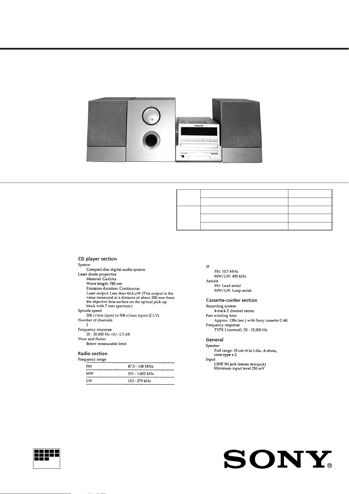
Photo : PMC-DR70L
TAPE Model Name Using Similar Mechanism NEW
Section T ape Tr ansport Mechanism Type MF-PMCDR50
CD
Section
AEP Model
UK Model
E Model
PMC-DR50L/DR70L
Tourist Model
PMC-DR50L
Model Name Using Similar Mechanism NEW
MD Mechanism Type KSM-213CCP
Optical Pick-up Type KSS-213C
SPECIFICATIONS
– Continued on page 2 –
MICROFILM
PERSONAL COMPONENT SYSTEM
Page 2

5-5. SCHEMATIC DIAGRAM – MAIN SECTION (1/3) –
p
p
r
Refer to page 74 for IC Block Diagram.
PMC-DR50L/DR70L
r
Waveforms – MAIN SECTION (1/3) –
1
1.5Vp-
75kHz
IC3 @¡
2
IC4 !¢
VOLT/DIV : 0.5 V AC
TIME/DIV : 5 msec
556mVp-
4.332MHz
VOLT/DIV : 0.2 V AC
TIME/DIV : 50 nsec
Note:
• All capacitors are in µF unless otherwise noted. pF: µµF
50 WV or less are not indicated except for electrolytics
and tantalums.
• All resistors are in Ω and 1/
specified.
¢
•
• U : B+ Line.
• H : adjustment for repair.
• Voltages and waveforms are dc with respect to ground
• Voltages are tak en with a V OM (Input impedance 10 MΩ).
• Waveforms are taken with a oscilloscope.
• Circled numbers refer to waveforms.
• Signal path.
: internal component.
under no-signal (detuned) conditions.
no mark : FM
( ) : MW
<>: LW
Voltage variations may be noted due to normal production tolerances.
Voltage variations may be noted due to normal production tolerances.
F : FM
f : MW
L : LW
4
W or less unless otherwise
– 39 – – 41 –– 40 –
Page 3
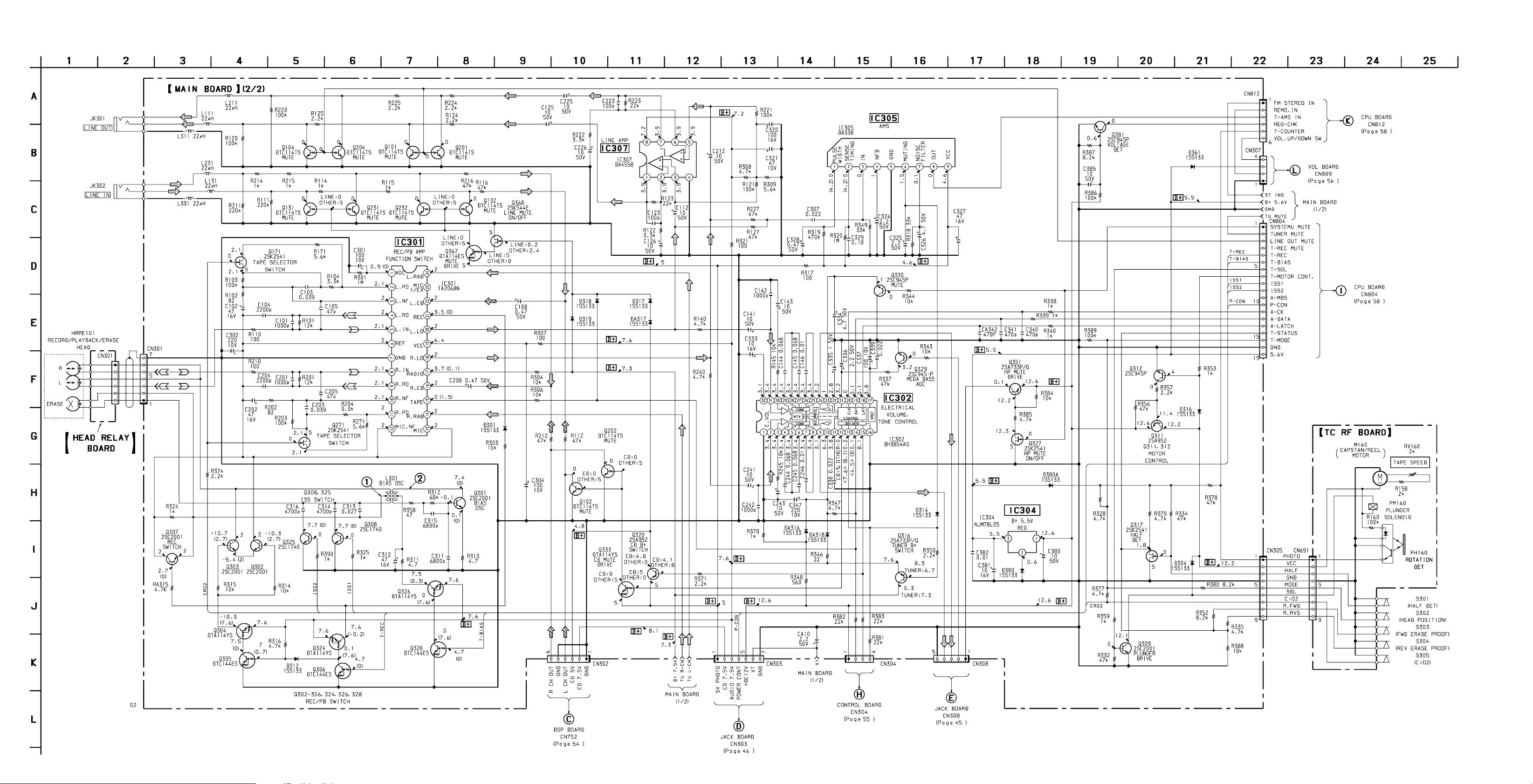
PMC-DR50L/DR70L
5-6. SCHEMATIC DIAGRAM – MAIN SECTION (2/3) –
r
Refer to page 74 for IC Block Diagrams.
r
Refer to page 45 for Waveforms.r Refer to page 45 for Notes.
– 42 – – 44 –– 43 –
Page 4

p
p
r
Waveforms – MAIN SECTION (2/3) –
1
60Vp-
57kHz
ATT : 1/10
L301
VOLT/DIV : 1V AC
TIME/DIV : 5 µsec
2
15Vp-
57kHz
5-7. SCHEMATIC DIAGRAM – MAIN SECTION (3/3) –
PMC-DR50L/DR70L
Q301 C
Note on Schematic Diagram – Main Section (2/3) – :
Note:
• All capacitors are in µF unless otherwise noted. pF: µµF
50 WV or less are not indicated except for electrolytics
and tantalums.
• All resistors are in Ω and 1/
specified.
• U : B+ Line.
• H : adjustment for repair.
• Voltages and waveforms are dc with respect to ground
under no-signal (detuned) conditions.
no mark : COMMON (REC)
( ) : PLAY
• Voltages are tak en with a V OM (Input impedance 10 MΩ).
Voltage variations may be noted due to normal production tolerances.
• Waveforms are taken with a oscilloscope.
Voltage variations may be noted due to normal production tolerances.
• Circled numbers refer to waveforms.
• Signal path.
F : FM
E : PB
a : REC
J : CD
VOLT/DIV : 5 V AC
TIME/DIV : 5 µsec
4
W or less unless otherwise
Note on Schematic Diagram – Main Section (3/3) – :
Note:
• All capacitors are in µF unless otherwise noted. pF: µµF
50 WV or less are not indicated except for electrolytics
and tantalums.
• All resistors are in Ω and 1/
specified.
• U : B+ Line.
• Voltages are dc with respect to ground under no-signal
(detuned) conditions.
no mark : FM
• Voltages are tak en with a V OM (Input impedance 10 MΩ).
Voltage variations may be noted due to normal production tolerances.
• Signal path.
F : FM
c : digital out
4
W or less unless otherwise
– 45 – – 47 –– 46 –
Page 5

5-9. SCHEMATIC DIAGRAM – CD SECTION –
r
Refer to page 75 -76 for IC Block Diagrams.
r
Refer to page 55 for Waveforms.
PMC-DR50L/DR70L
– 51 – – 52 – – 54 –– 53 –
Note:
• All capacitors are in µF unless otherwise noted. pF: µµF
50 WV or less are not indicated except for electrolytics
and tantalums.
• All resistors are in Ω and 1/
specified.
Note: The components identified by mark ! or dotted
line with mark ! are critical for safety.
Replace only with part number specified.
• U : B+ Line.
• Voltages and waveforms are dc with respect to ground
under no-signal (detuned) conditions.
no mark : CD STOP
( ) : CD PLAY
• Voltages are tak en with a V OM (Input impedance 10 MΩ).
Voltage variations may be noted due to normal production tolerances.
• Waveforms are taken with a oscilloscope.
Voltage variations may be noted due to normal production tolerances.
• Circled numbers refer to waveforms.
• Signal path.
J : CD
c : digital out
4
W or less unless otherwise
Page 6

PMC-DR50L/DR70L
p
µ
p
p
5-10. SCHEMATIC DIAGRAM – CONTOROL SECTION –
r
Waveforms (CD SECTION)
(RFO)
(FEO)
(PLAY MODE)
1.0 – 1.5Vp-p
VOLT/DIV : 0.5 V AC
TIME/DIV : 1 µsec
(PLAY MODE)
VOLT/DIV : 1 V AC
TIME/DIV : 1 msec
(PLAY MODE)
1
IC701 #£
2
IC701 6
3
0.6Vp-p
0.7Vp-
r
Waveforms – CONTROL SECTION –
1
4.8Vp-p
32.768kHz
IC801 $™
VOLT/DIV : 1V AC
TIME/DIV : 10 µsec
2
2.5Vp-
8MHz
IC801 $º
VOLT/DIV : 0.5V AC
TIME/DIV : 50 nsec
IC701 $∞
(TO)
4
IC751 @ª
(PCO)
5
IC751 #ª, $º
(LRCK)
6
IC751 &¡
(XTAO)
0.1162MHz
8.6
sec
16.9344MHz
VOLT/DIV : 20mV AC
TIME/DIV : 1 msec
VOLT/DIV : 0.5 V AC
TIME/DIV : 5 µsec
µ
sec
22.85
VOLT/DIV : 1 V AC
TIME/DIV : 5 µsec
VOLT/DIV : 0.1V AC
TIME/DIV : 20 nsec
875mVp-p
4.7Vp-p
271mVp-
Note:
• All capacitors are in µF unless otherwise noted. pF: µµF
50 WV or less are not indicated except for electrolytics
and tantalums.
• All resistors are in Ω and 1/
specified.
• U : B+ Line.
• Voltages and waveforms are dc with respect to ground
under no-signal (detuned) conditions.
no mark : RADIO (COMMON)
( ) : CD
< > : REC
[ ] : PLAY
• V oltages are taken with a V OM (Input impedance 10 MΩ).
Voltage variations may be noted due to normal production tolerances.
• Waveforms are taken with a oscilloscope.
Voltage variations may be noted due to normal production tolerances.
• Circled numbers refer to waveforms.
4
W or less unless otherwise
– 57 – – 58 –– 55 – –56 –
Page 7

5-13. SCHEMATIC DIAGRAM – AMP SECTION –
PMC-DR50L/DR70L
– 65 – – 67 –– 66 –
Note:
• All capacitors are in µF unless otherwise noted. pF: µµF
50 WV or less are not indicated except for electrolytics
and tantalums.
• All resistors are in Ω and 1/
specified.
• 2 : nonflammable resistor.
Note: The components identified by mark ! or dotted
line with mark ! are critical for safety.
Replace only with part number specified.
• U : B+ Line.
• Voltages are dc with respect to ground under no-signal
(detuned) conditions.
no mark : FM
• V oltages are taken with a V OM (Input impedance 10 MΩ).
Voltage variations may be noted due to normal production tolerances.
• Signal path.
F : FM
4
W or less unless otherwise
Page 8

5-15. SCHEMATIC DIAGRAM – WOOFER AMP SECTION – (DR70L ONLY)
r
Refer to page 76 for IC Block Diagram.
PMC-DR50L/DR70L
Note:
• All capacitors are in µF unless otherwise noted. pF: µµF
50 WV or less are not indicated except for electrolytics
and tantalums.
• All resistors are in Ω and 1/
specified.
• U : B+ Line.
• Voltages are dc with respect to ground under no-signal
(detuned) conditions.
no mark : FM
• Voltages are tak en with a V OM (Input impedance 10 MΩ).
Voltage variations may be noted due to normal production tolerances.
• Signal path.
F : FM
4
W or less unless otherwise
– 71 – – 73 –– 72 –
Page 9

PMC-DR50L/DR70L
R
I
I
r
IC Block Diagrams – MAIN SECTION (2/3) –
IC301 TA2068N
AGC
IC302 BH3854AFS
FILTE
32
AGND
L.RAD
MIC
I/EX
23 22 21
15k
RADIO
LINE
TAPE
BUF AMP
A1
NAB
AMP1
L.NF
L.PO
IN2
30
31
IN1
L.CD
10k
6k
NF2
NF2
REC
L.LO
2024
1k 1k
MONITOR
AMP
10k
10k
10k
10k
26dB
29
4321
7dB
MUTE
BUF AMP
B1
10k 10k
ALC1
REC
AMP1
REF AMP
4 5 6321
L.IN
L.RO
DVN2
BIN2
28
27 26 25 24 23 20 19 18 17
TONE
MATRIX
SURROUND
TONE
6 7 8 9 10 11 12 13 14 15 16
5
BIN1
BVN1
REF
BVO2
BVO1
LOGIC
ON
RADIO
R.LO
VCC
1819 14 13
MONITOR
AMP
7dB
ON
MUTE
BUF AMP
B2
ALC2
TVO2
TVO1
REC
AMP2
R.IN
VR
VR
26dB
OUT2
OUT1
DET
2.1
GND
TIN2
TIN1
R.CD
10k
1k
6k
10k
RADIO
TAPE
10k
10k
BUF AMP
A2
10k
MUTE
ON
NAB
AMP2
987 10 11 12
R.RO
VC
TC
22 21
CONTROL
SC
VCC
R.NF
151617
LINE
TAPETAPE
TAPE
10k
R.PO
BC
PORT1
R.RAD
10k
MIC
AMP1
1k
CLK
PORT2
MIC
MIC
NF
DATA
PORT3
IC305 BA338
VCC
OUT
NOISE FILTER
MUTING
GND
NFB
9 8 7 6 5 4 3 2 1
LATCH
VREF
DGND
PORT4
IN
PRE AMP
S
B+
R
F.F.
COMPARATOR
Q
COMPARATOR
COMPARATOR
SENSE TIMING
PULSE WIDTH
r
IC Block Diagrams – CD SECTION –
IC701 CXA1992BR
PD1
38 37 36 35 34 33 32 31 30 29 28 27
PD1 IV
AMP
VCC
VCC
IFB1
VEE
TGFL
E-F BALANCE
WINDOW COMP.
DFCT
TM1
FEI
F. BIAS
GND
LPFI
ATSC
TZC
TDFCT
FZC
PD2
39
PD2 IV
AMP
40
41
F
42
E
43
EI
VEE
44
45
TO
46
47
TI
48
49
50
51
VC
52
E IV AMP
BAL1
TOG1
TOG2
TZC COMP.
VCC
FZC COMP.
F IV AMP
BAL3
BAL2
BAL4
TOG4
TOG3
ATSC
WINDOW
COMP.
VCC
VEE
1 2 3 4 5 6 7 8 9 10 11 12 13
FEO
IC702 BA6898FP
GND
F-
F+
FIN
NC
2728 26 25 24 23
D
D D
LEVEL SHIFT
VREF
PD
VEE
APC
LASER POWER CONTROL
IFB4
IFB5
IFB2
IFB3
TRK. GAIN
WINDOW COMP.
TG1
DFCT
FS4
FDFCT
VCC
22
VCC
LD
VEE
FGD
RFTC
FE AMP
IFB6
FO. BIAS
WINDOW
COMP.
TRACKING
PHASE COMPENSATION
FOCUS
PHASE COMPENSATION
FLB
VCC
NC
21 20 19
VCC
RFO
RF-
RF
SUMMING
AMP
FOK
LDON
FOH
FOL
TGH
TGL
BALH
BALL
ATSC
TZC
FZC
FE_O
TIN
18 17 16 15
D
LEVEL SHIFT
LPCL
FE-
T-
T+
VEE
LEVEL S
VCC
DFCTO
FS2
NC
RFI
VEE
MIRR
LPC
TGFL
IIL DATA REGISTER,
INPUT SHIFT REGISTER,
ADDRESS DECODER,
SENS SELECTOR,
OUTPUT DECODER
IFB1-6
BAL1-4
TOG1-4
VCC
FS1
Charge
up
VEE
SRCH
NC
SPIN
CP
VCC
TGU
CB
VCC
VEE
DFCT
IIL
↓
TTL
MIRR
DFCT1
FS1-4 TG1-2 TM1-7 PS1-4
TM7
TG2
FSET
FSET
TG2
CC1
CC1
CC2
VCC VCC
TM4 TM6
TM3
TE-
FOK
IIL
TTL
TTL
IIL
ISET
VEEVEE
TEO
IC751 CXD2589Q
PCMD
PCMD
BCK
BCKI
VSS
VDD
XUGF
XPCK
GFS
C2PO
XTSL
C4M
DOUT
DIGITAL
OUT
DATA
XLAT
EMPH
CLOK
SEIN
ERROR
CORRECTOR
SERVO
AUTO
SEQUENCER
CNIN
DATO
EFM
DEMODULATOR
D/A
INTERFACE
CLOCK
GENERATOR
XLTO
CLKO
RAM
SPOA
16K
SPOB
XLON
FOK
VDD
ASYMMETRY
CORRECTOR
DIGITAL
PLL
OSC
DIGITAL
CLV
VSS
40
LRCKI
39
LRCK
ASYO
38
37
ASYI
BIAS
36
35
RF
34
AVDD
33
CLTV
32
AVSS
31
FILI
30
FILO
29
PCO
28
VCTL
27
V16M
26
VCKI
VPCO
25
TES1
24
23
TEST
22
PWMI
21
MDP
WFCK
SCOR
SBSO
VSS
60
61
VDD
SYSM
62
26
SENS2
63
AVSS
24
TM2
SENS1
64
24
C. OUT
23
XRST
22
DATA
21
XLT
20
CLK
19
LOCK
VCC
18
ISET
17
16
SLO
SL-
15
14
SL+
AVDD
AOUT1
AIN1
LOUT1
AVSS
XVDD
XTAI
XTAO
XVSS
AVSS
LOUT2
AIN2
AOUT2
AVDD
AVSS
XRST
VDD
65
66
67
68
69
70
71
72
73
74
75
76
77
78
79
80
↓
↓
VCC
TM5
TIMING
LOGIC
PWM
PWM
EXCK
59 58 57 56 55 54 53 52 51 50 49 48 47 46 45 44 43 42 41
123 456789 1011121314 15 16 17 18 19 20
VSS
LMUTE
RMUTE
ENPHI
SERIAL-IN
INTERFACE
OVER SAMPLING
DIGITAL FILTER
3rd-ORDER
NOISE SHAPER
SUB CODE
PROCESSOR
CPU
INTERLACE
SENS
SQCK
SQSO
IC651 TA8409S
r
IC Block Diagrams
– WOOFER AMP SECTION –
STANDBY
BLOCK
VREF
BLOCK
IC601 TDA2052
T. S. D.
MUTE
DRIVER
MUTE
GND
LEVEL SHIFT
DD
NC
SIN
REGULATOR, BIAS,
T. S. D. MONITOR
LEVEL SHIFT
DD
21 3 4 5 6 7 8 9 10 11 12 13 14
SL-
SL+
SLIN
RST
REG –B
REGD
– 74 – – 76 –– 75 –
SP-
SP+
GND
SPO
HEAT
CUT OFF
BLOCK
2 3
1
VCC OUT2 NC GND
IN2
MUTE/
ST-BY
3 4 5 6 721
IN–
OUT
VDD
5 6
4
7
VS
OUT1 VREF IN1
8
9
MUTE/
STANDBY
VEE
IN1+
IN2+
 Loading...