

Page 1
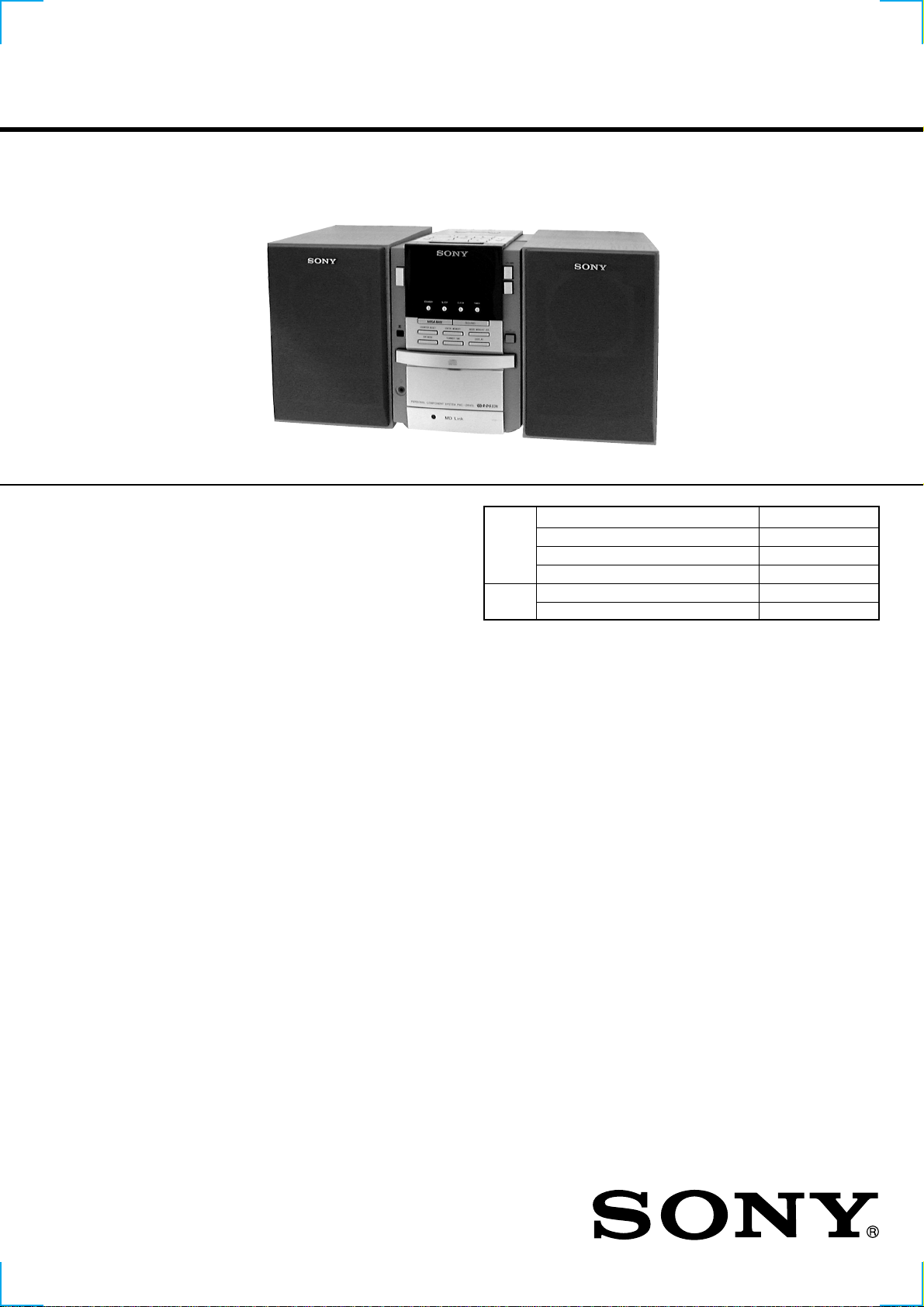
PMC-DR45
SERVICE MANUAL
AUDIO POWER SPECIFICATIONS
POWER OUTPUT AND TOTAL
HARMONIC DISTORTION
With 4-ohm loads, both channels driven from
150 - 10,000 Hz; rated 13 W per channelminimum RMS power, with no more than 10%
total harmonic distortion in AC operation.
CD
Section
Tape
Section
US Model
Canadian Model
Model Name Using Similar Mechanism CFD-S47
CD Loading Mechanism Type FLM-DR45-149
CD Mechanism Type KSM-213CCP
Optical Pick-up Name KSS-213C
Model Name Using Similar Mechanism NEW
Tape Transport Mechanism Type MF-DR45
CD player section
System
Compact disc digital audio system
Laser diode properties
Material: GaAlAs
Wave length: 780 nm
Emission duration: Continuous
Laser output: Less than 44.6 µW
(This output is the value measured at a distance of
about 200 mm from the objective lens surface on
the optical pick-up block with 7 mm aperture.)
Spindle speed
200 r/min (rpm) to 500 r/min (rpm) (CLV)
Number of channels
2
Frequency response
20 - 20,000 Hz +0/–1 dB
Wow and flutter
Below measurable limit
Radio section
Frequency range
FM: 87.6 - 108 MHz
AM:530 - 1,710 kHz
Antennas
FM: Lead antenna
AM:Loop antenna
SPECIFICATIONS
Cassette-corder section
Recording system
4-track 2-channel stereo
Fast winding time
Approx. 120 s (sec.) with Sony cassette C-60
Frequency response
TYPE I (normal): 50 - 14,000 Hz
General
Speaker
Full range: 8 cm (3
cone type × 2
Input
LINE IN jack (stereo minijack)
Minimum input level 440 mV
Outputs
Headphones jack (stereo minijack)
For 16 - 64 ohms impedance headphones
LINE OUT jack (stereo minijack)
Rated output level 330 mV at load impedance
47 kilohms
OPTICAL DIGITAL OUT (CD) (optical output connector)
Wave length: 760 - 880 nm
Power output (excluding US model)
15 W + 15 W (at 4 ohms, 10% harmonic distortion
in AC operation)
1/4 in.) dia., 4 ohms,
– Continued on next page –
PERSONAL COMPONENT SYSTEM
– 1 –
Page 2

Power requirements
For personal component system:
120 V AC, 60 Hz
For remote control:
3 V DC, 2 AA (size R6) batteries
Power consumption
AC 45 W (US model)
AC 50W (Canadian model)
Dimensions (incl. projecting parts)
Player: approx. 137 × 202 × 212 mm (w/h/d)
1/2 × 8 × 8 3/8 inches)
(5
Left speaker: approx. 137 × 202 × 212 mm
(w/h/d) (5
Right speaker: approx. 137 × 202 × 180 mm
(w/h/d) (5
Mass
Player: approx. 1.8 kg (3 lb. 15 oz.)
Left speaker: approx. 3 kg (6 lb. 10 oz.)
Right speaker: approx. 1.5 kg (3 lb. 5 oz.)
Supplied accessories
Remote control (1) (RMT-CDR45A)
FM lead antenna (1)
AM loop antenna (1)
Audio connecting cord (1)
Design and specifications are subject to change without
notice.
1/2 × 8 × 8 3/8 inches)
1/2 × 8 × 7 1/8 inches)
TABLE OF CONTENTS
1. SERVICING NOTES......................................................... 3
2. GENERAL
Playing a CD ........................................................................... 4
Listening to the radio............................................................... 4
Playing a tape .......................................................................... 5
Recording on a tape ................................................................. 5
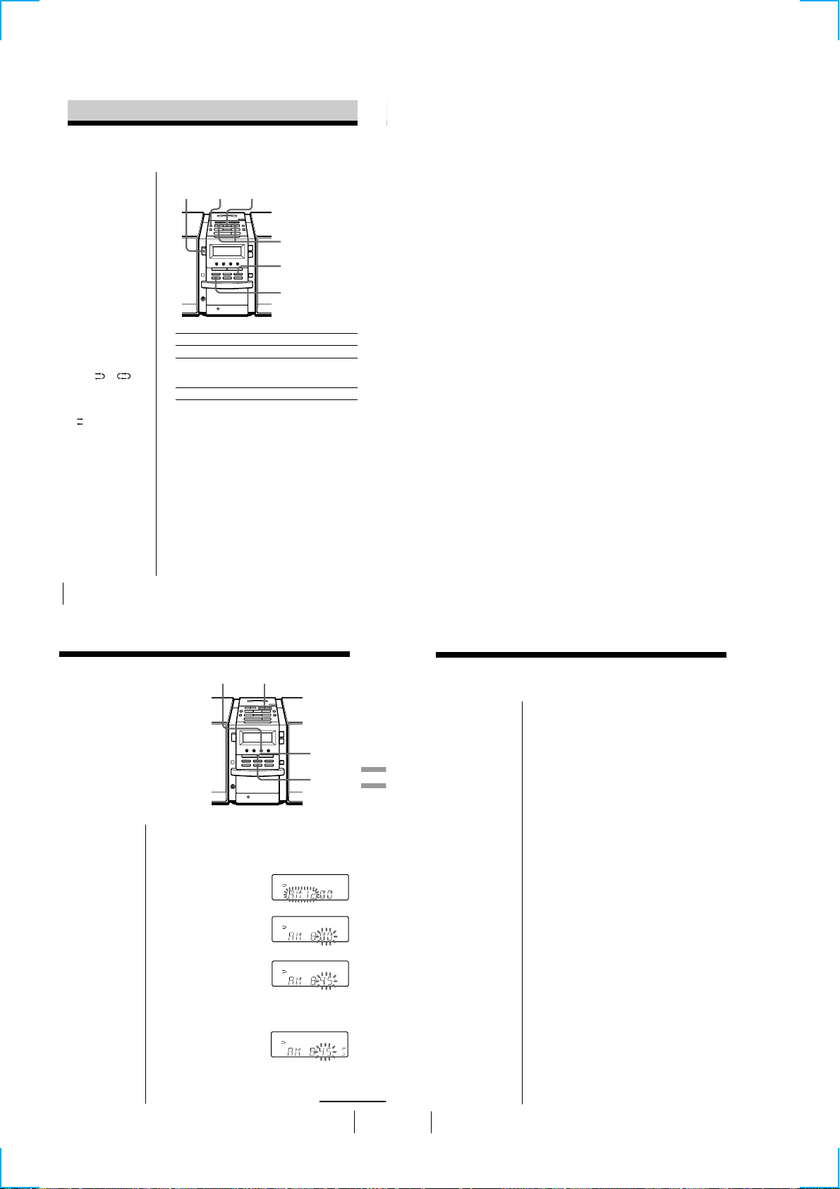
Setting the clock ...................................................................... 6
3. DISASSEMBLY
3-1. Cabinet (Front) Assy ........................................................... 7
3-2. Cabinet (Rear) ..................................................................... 8
3-3. Front Board ......................................................................... 8
3-4. Control Board ...................................................................... 9
3-5. Line Board........................................................................... 9
3-6. Tuner Board....................................................................... 10
3-7. Holder, Cassette ................................................................ 10
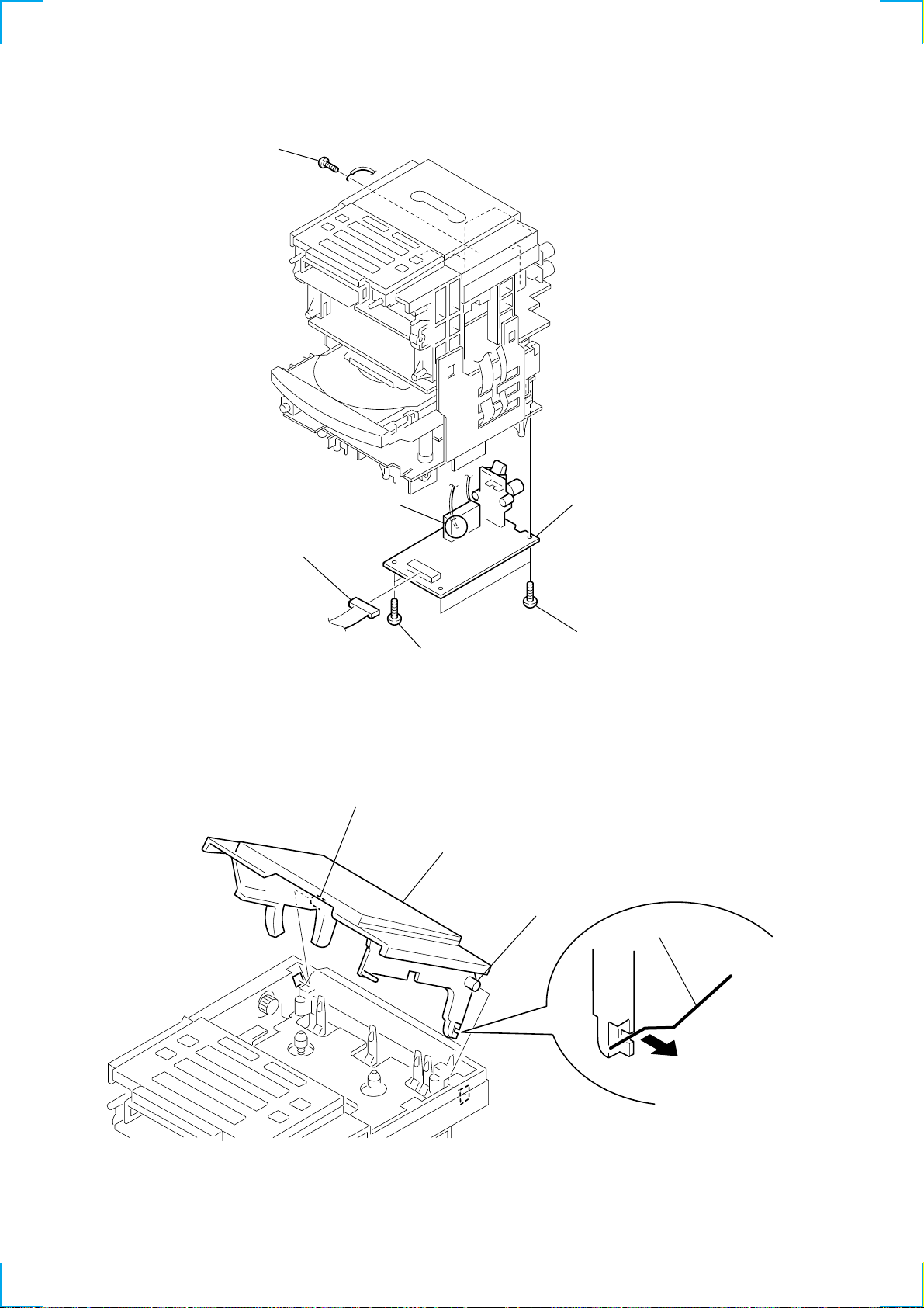
3-8. Top Block Assy ................................................................. 11
3-9. CD Assy, H/P Board.......................................................... 11
3-10. Main Board ....................................................................... 12
3-11. Tape Mechanism Block..................................................... 12
3-12. Top Board.......................................................................... 13
3-13. “Plate Assy, Chuck”, Tray................................................. 13
3-14. Loading Board................................................................... 14
3-15. CD Board .......................................................................... 14
3-16. CD Mechanism Block ....................................................... 15
3-17. Power Board ...................................................................... 15
4. MECHANICAL ADJUSTMENTS............................... 16
5. ELECTRICAL ADJUSTMENTS
5-1. Tape Section ...................................................................... 16
5-2. Tuner Section .................................................................... 18
5-3. CD Section ........................................................................ 20
6. DIAGRAMS
6-1. IC Pin Descriptions ........................................................... 21
6-2. Circuit Boards Location .................................................... 23
6-3. Block Diagram –Tuner Section–....................................... 25
6-4. Block Diagram –CD Section–........................................... 27
6-5. Block Diagram –Tape Section– ........................................29
6-6. Block Diagram –System Control, Power Section– ........... 31
6-7. Printed Wiring Board –Tuner Section–............................. 33
6-8. Schematic Diagram –Tuner Section–................................ 35
6-9. Printed Wiring Boards –CD Section– ............................... 37
6-10. Schematic Diagram –CD Section–.................................... 39
6-11. Printed Wiring Board –TC Section– ................................. 41
6-12. Schematic Diagram –TC Section– .................................... 43
6-13. Printed Wiring Board –Main Section– .............................. 45
6-14. Schematic Diagram –Main Section–................................. 47
6-15. Printed Wiring Board –Control Section– ..........................49
6-16. Schematic Diagram –Control Section– .............................53
6-17. Printed Wiring Board –Front Section– ..............................55
6-18. Schematic Diagram –Front Section– ................................ 56
6-19. Printed W iring Board –Top Section– ................................ 57
6-20. Schematic Diagram –Top Section–................................... 58
6-21. Printed Wiring Board –Line Section– ............................... 59
6-22. Schematic Diagram –Line Section– ..................................59
6-23. Printed Wiring Boards –Power Section–........................... 61
6-24. Schematic Diagram –Power Section– ............................... 63
6-25. IC Block Diagrams............................................................65
7. EXPLODED VIEWS
7-1. Cabinet Section .................................................................69
7-2. Cabinet (T op) Section .......................................................70
7-3. CD Chassis Section ........................................................... 71
7-4. Mechanism Deck Section (1) ............................................ 72
7-5. Mechanism Deck Section (2) ............................................ 73
7-6. Optical Pick-up Section .................................................... 74
7-7. Speaker (L) Section...........................................................75
7-8. Speaker (R) Section........................................................... 76
8. ELECTRICAL PARTS LIST......................................... 77
– 2 –
Page 3
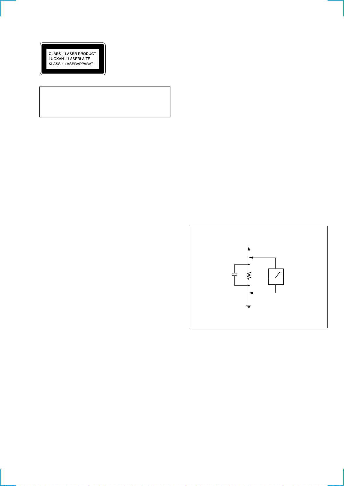
SECTION 1
SERVICING NOTES
This Compact Disc player is
classified as a CLASS 1
LASER product.
The CLASS 1 LASER
PRODUCT lable is located
on the bottom exterior.
CAUTION
Use of controls or adjustments or performance of procedures other than those specified herein may result in hazardous radiation exposure.
Flexible Circuit Board Repairing
• Keep the temperature of the soldering iron around 270˚C during
repairing.
• Do not touch the soldering iron on the same conductor of the
circuit board (within 3 times).
• Be careful not to apply force on the conductor when soldering
or unsoldering.
Notes on Chip Component Replacement
• Never reuse a disconnected chip component.
• Notice that the minus side of a tantalum capacitor may be dam-
aged by heat.
NOTES ON HANDLING THE OPTICAL PICK-UP BLOCK
OR BASE UNIT
The laser diode in the optical pick-up block may suffer electrostatic
breakdown because of the potential difference generated by the
charged electrostatic load, etc. on clothing and the human body.
During repair , pay attention to electrostatic breakdown and also use
the procedure in the printed matter which is included in the repair
parts.
The flexible board is easily damaged and should be handled with
care.
NOTES ON LASER DIODE EMISSION CHECK
The laser beam on this model is concentrated so as to be focused on
the disc reflective surface by the objective lens in the optical pickup block. Therefore, when checking the laser diode emission,
observe from more than 30 cm away from the objective lens.
SAFETY CHECK-OUT
After correcting the original service problem, perform the following
safety check before releasing the set to the customer:
Check the antenna terminals, metal trim, “metallized” knobs, screws,
and all other exposed metal parts for AC leakage. Check leakage as
described below.
LEAKAGE TEST
The AC leakage from any exposed metal part to earth ground and
from all exposed metal parts to any exposed metal part having a
return to chassis, must not exceed 0.5 mA (500 microamperes).
Leakage current can be measured by any one of three methods.
1. A commercial leakage tester, such as the Simpson 229 or RCA
WT-540A. Follow the manufacturers’ instructions to use these
instruments.
2. A battery-operated AC milliammeter. The Data Precision 245
digital multimeter is suitable for this job.
3. Measuring the voltage drop across a resistor by means of a VOM
or battery-operated AC voltmeter . The “limit” indication is 0.75
V , so analog meters must have an accurate low-voltage scale. The
Simpson 250 and Sanwa SH-63Trd are examples of a passive
VOM that is suitable. Nearly all battery operated digital
multimeters that have a 2V AC range are suitable. (See Fig. A)
To Exposed Metal
Parts on Set
0.15µF
Ω
1.5k
Earth Ground
AC
voltmeter
(0.75V)
SAFETY-RELATED COMPONENT WARNING!!
COMPONENTS IDENTIFIED BY MARK 0 OR DOTTED LINE
WITH MARK 0 ON THE SCHEMATIC DIAGRAMS AND IN
THE PARTS LIST ARE CRITICAL TO SAFE OPERATION.
REPLACE THESE COMPONENTS WITH SONY PARTS WHOSE
P ART NUMBERS APPEAR AS SHOWN IN THIS MANU AL OR
IN SUPPLEMENTS PUBLISHED BY SONY.
ATTENTION AU COMPOSANT AYANT RAPPORT
À LA SÉCURITÉ!!
LES COMPOSANTS IDENTIFIÉS P AR UNE MARQUE 0 SUR LES
DIAGRAMMES SCHÉMA TIQ UES ET LA LISTE DES PIÈCES SONT
CRITIQUES POUR LA SÉCURITÉ DE FONCTIONNEMENT. NE
REMPLACER CES COMPOSANTS QUE PAR DES PIÈCES SONY
DONT LES NUMÉROS SONT DONNÉS DANS CE MANUEL OU
DANS LES SUPPLÉMENTS PUBLIÉS PAR SONY.
Fig. A. Using an AC voltmeter to check AC leakage.
– 3 –
Page 4
Basic Operations
SECTION 2
GENERAL
This section is extracted
from instruction manual.
Playing a CD
21
For hookup instructions, see pages 32 - 36.
1 Press Z CD OPEN/CLOSE
2 Press u.
(direct power-on) and place the
CD on the CD tray.
(On the remote, press N on the
CD section.)
The CD tray closes and the player
plays all the tracks once.
With the label side up
Display
Playing timeTrack number
Tip
Next time you want to
listen to a CD, just press
u. The player turns on
automatically and starts
playing the CD.
Use these buttons for additional operations
u
POWER
To Press
adjust the volume VOLUME +, –
stop playback x
pause playback u
go to the next track >
go back to the previous track .
remove the CD Z CD OPEN/CLOSE
turn on/off the player POWER
., >
(VOL +, – on the remote)
(X on the remote)
Press again to resume play
after pause.
x
VOLUME +, –
Z CD
OPEN/CLOSE
Basic Operations
Basic Operations4
Listening to the radio
1
For hookup instructions, see pages 32 - 36.
1 Press BAND•AUTO PRESET
2 Hold down TUNE TIME SET + or
until the band you want appears
in the display (direct power-on).
– (TUNE + or – on the remote)
until the frequency digits begin to
change in the display.
The player automatically scans
the radio frequencies and stops
when it finds a clear station.
If you cannot tune in a station,
press the button repeatedly to
change the frequency step by
step.
2
Display
Indicates an FM
stereo broadcast.
Tips
• The “FM1” and “FM2”
bands have the same
functions. You can store
the stations you want
separately in “FM1” and
“FM2”.
• If the FM broadcast is
noisy, press MODE until
“MONO” appears in the
display and the radio
will play in monaural.
• Next time you want to
listen to the radio, just
press the BAND•AUTO
PRESET button. The
player turns on
automatically and starts
playing the previous
station.
Basic Operations
Use these buttons for additional operations
POWER
To Press
adjust the volume VOLUME +, –
turn on/off the radio POWER
To improve broadcast reception
FM:
Keep the FM lead antenna as horizontal as possible
and reorient it.
If the FM broadcast is still noisy, disconnect the FM
lead antenna and connect the FM outdoor antenna
(not supplied) (page 36).
AM:
Keep the AM loop antenna as far as possible from the
player and reorient it.
MODE
VOLUME +, –
(VOL +, – on the remote)
5
Basic Operations
Basic Operations6
Basic Operations
7
– 4 –
Page 5
Playing a tape
Use these buttons for additional operations
POWER Z PUSH OPEN/CLOSE
1, 2
3
TAPE m, M
x
n
VOLUME +, –
COUNTER RESET
DIR MODE
Basic Operations
For hookup instructions, see pages 32 - 36.
1 Press Z PUSH OPEN/CLOSE to
2 Press Z PUSH OPEN/CLOSE to
3 Press N.
Basic Operations8
open the tape compartment and
insert a recorded tape. Use TYPE I
(normal), TYPE II (high position)
and TYPE IV (metal) tapes.
close the compartment.
(On the remote, press TAPE N.)
The player turns on (direct
power-on) and starts playing.
Recording on a tape
3
3 3
For hookup instructions, see pages 32 - 36. To record on a
MiniDisc or DAT recorder, connect the component (see
page 38).
1 Press Z PUSH OPEN/CLOSE to
open the tape compartment, and
insert a blank tape. Use TYPE I
(normal) tape only.
Press Z PUSH OPEN/CLOSE
again to close the compartment.
1
With the side you want
to play facing up
Display
Tape counter
With the side you want
to record on facing up
Tips
• Press COUNTER RESET
to reset the counter to
“000”.
• Next time you want to
listen to a tape, just
press N or n. The
player turns on
automatically and starts
playing the tape.
To Press
adjust the volume VOLUME +, –
stop playback x
play the reverse side n
fast-forward or rewind the tape TAPE M or m
eject the cassette Z PUSH OPEN/CLOSE
turn on/off the player POWER
To select the direction mode of the tape
Press DIR MODE repeatedly.
To play Display shows
one side of the tape
both sides of the tape
from the upper side to reverse
side only
both sides of the tape repeatedly
3 Start recording.
To record the whole CD
Press CD DUBBING.
When
is displayed:
If the tape is reversed with the
recording of the track unfinished,
the player will record the track
again from its beginning on the
reverse side.
When
is displayed:
If the tape reaches to its end, the
player stops.
To record the radio
(You can also record the CD
according to the following
procedure. Play the CD after the
tape starts recording.)
Press z/X and then N.
To record on the reverse side,
press n.
(On the remote, while keeping
z/X pressed, press TAPE N or
n.)
(VOL +, – on the remote)
Basic Operations
m
9
Basic Operations
2 Select the program source you
Basic Operations10
want to record.
To record from the CD player:
Insert a CD (see page 4) and press
x on the CD section.
To record from the radio:
Tune in the station you want (see
page 6).
Display
– 5 –
continued
Basic Operations
11
Page 6
Recording on a tape (continued)
Use these buttons for additional operations
POWER
z/X
x
n,
N
MODE
DIR MODE
Tips
• Adjusting the volume or
the audio emphasis
(page 22) will not affect
the recording level.
• When
or is
displayed, recording
will be made on both
sides of the tape. To
record on one side, press
DIR MODE to display
.
• If the AM radio makes a
whistling sound after
you’ve pressed z/X in
step 3, press MODE to
select the position that
most decreases the
noise.
Note
When you start
recording using CD
DUBBING, you cannot
set the player in pause.
Basic Operations12
The Timer
Setting the clock
“– –:– –” indication appears in the
display until you set the clock.
To Press
stop recording x on the tape section
pause recording z/X
turn on/off the player POWER
To erase a recording, proceed as follows:
1 Insert a tape you want to erase its recording into the tape
deck and press x on the tape section.
2 On the player: press z/X and then N.
On the remote: While keeping z/X pressed, press
TAPE N.
CLOCK
Press the button again to
resume recording.
TUNE TIME SET –, +
ENTER
MEMORY
SUMMER
TIME
Setting the clock (continued)
Audio Emphasis/The Timer
To change the display to the daylight saving time
(summer time) indication
Press and hold SUMMER TIME for 2 seconds.
“SUMMER ON ” appears in the display for a few
seconds.
To cancel the summer time indication
Press and hold SUMMER TIME again.
“SUMMER OFF” appears in the display for a few
seconds.
Tip
The time display
system of this player is
the 12-hour system.
Before you begin, hook up the system (see pages 32 -
36).
1 Press and hold CLOCK until the hour digit flashes.
2 Set the clock.
1 Press TUNE TIME SET
+ or – to set the hour
and press ENTER
MEMORY.
2 Press TUNE TIME SET
+ or – to set the
minutes.
3 If you are on daylight saving time, press SUMMER
TIME.
m
4 Press ENTER MEMORY.
The clock starts from 00 seconds.
continued
The Timer 23
The Timer24
– 6 –
Page 7
SECTION 3
2
DISASSEMBLY
• The equipment can be removed using the following procedure.
Set Cabinet (Front) Assy
Cabinet (Rear)
Front Board
Control Board
Tuner Board
Line Board
Holder, Cassette
Top Block Assy
Main Board
CD Assy, H/P Board
Loading Board CD Board CD Mechanism Block
Speaker Set Power Board
Note : Follow the disassembly procedure in the numerical order given.
Tape Mechanism Block
(TC Board)
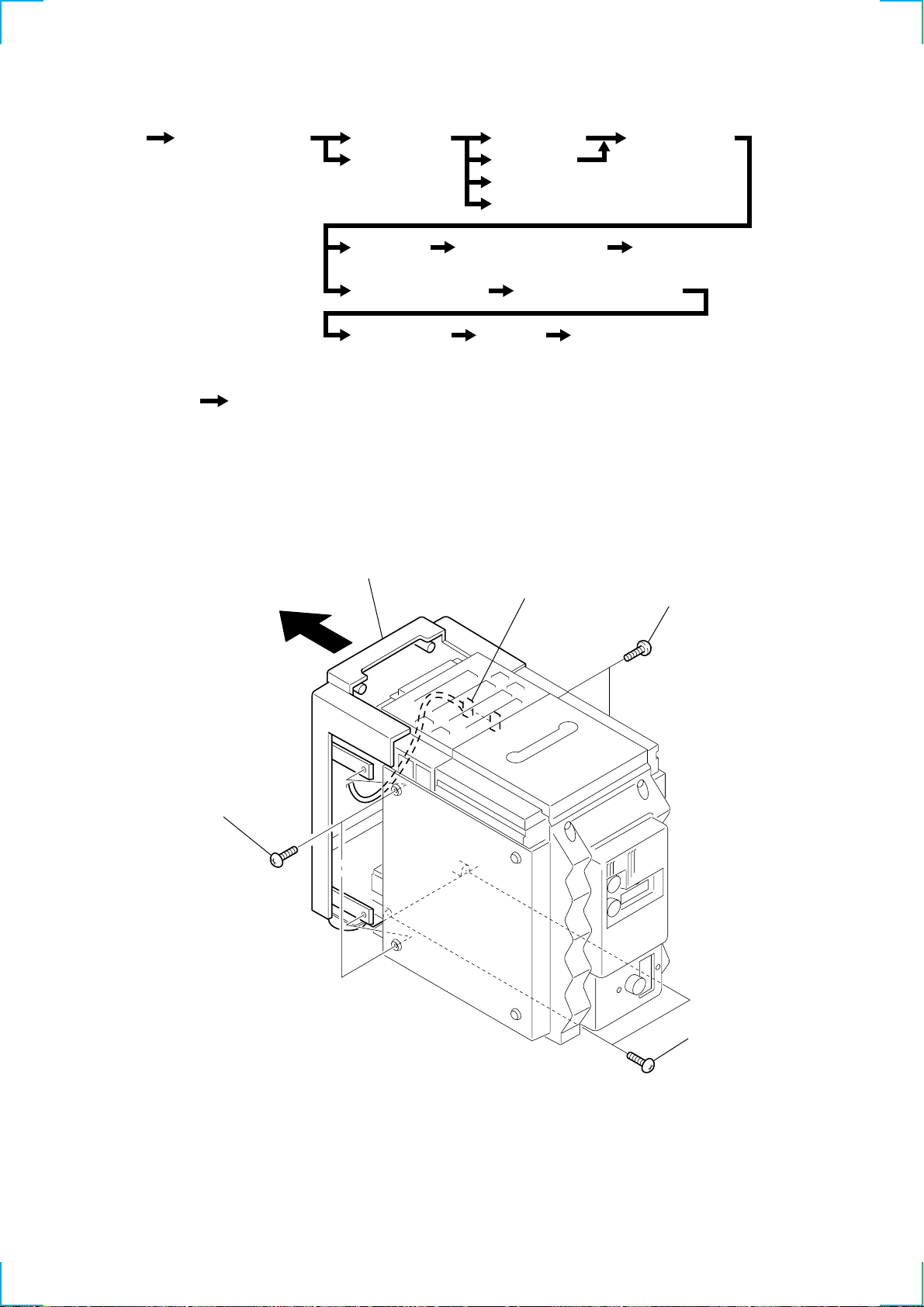
3-1. CABINET (FRONT) ASSY
5 cabinet (front) assy
Top Board
“Plate Assy, Chuck”, Tray
4 CNP802
1 BVTP 3x12
2 BVTP 3x12
3 BVTP 3x1
– 7 –
Page 8
3-2. CABINET (REAR)
0
d
4 cabinet (rear)
3 BVTP 3x10
2 BVTP 3x1
3-3. FRONT BOARD
1 BVTP 3x10
1 BTP 2.6x8
2 BTP 2.6x8
3 FRONT boar
– 8 –
Page 9
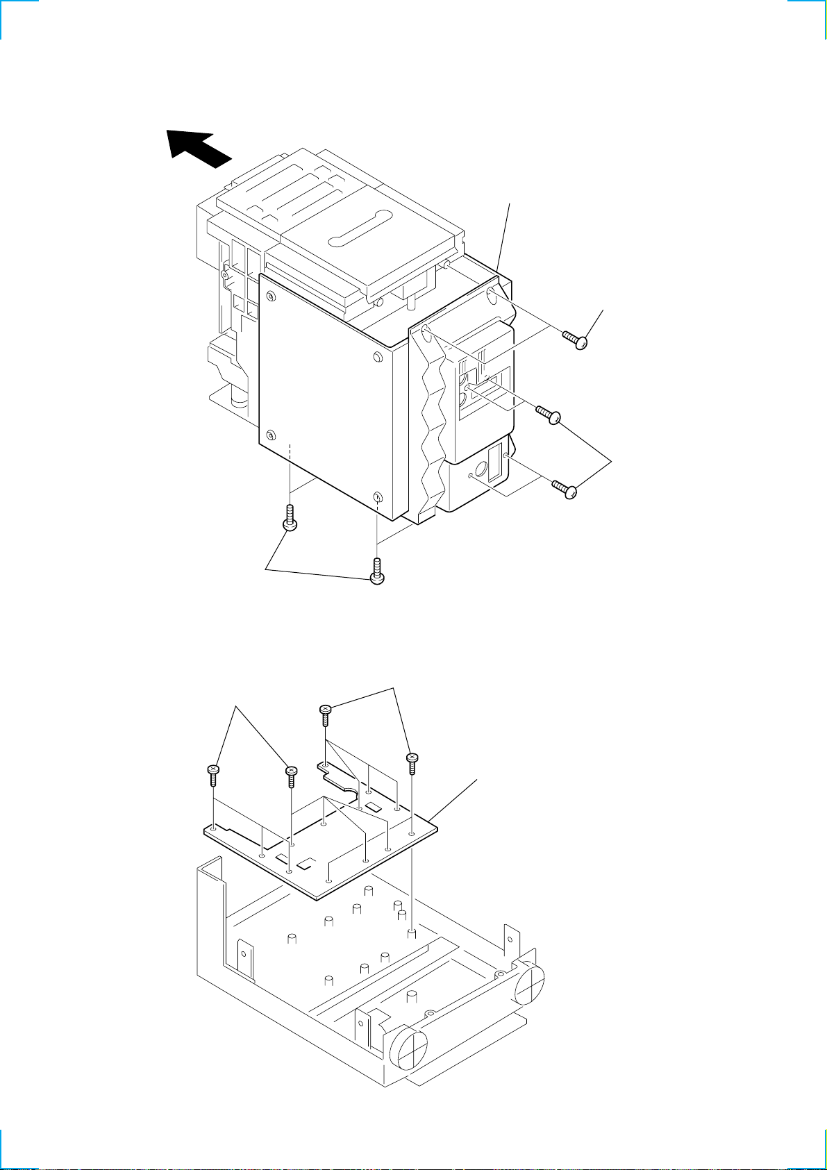
3-4. CONTROL BOARD
5 CONTROL board
4 BVTP 3x10
1 CNP804
2 CNP803
6 CNP307
3 BVTP 3x10
3-5. LINE BOARD
1 CNP304
MAIN board
3 CNP312
4 LINE board
– 9 –
2 BVTP 3x10
Page 10
3-6. TUNER BOARD
1 screw
3-7. HOLDER, CASSETTE
5 Removal the solder.
4 CNP1
2 boss
6 TUNER board
2 BVTP 3x10
3 BVTP 3x10
4 holder, cassette
3 boss
1 spring, cassette
– 10 –
Page 11
3-8. TOP BLOCK ASSY
1 CNP306
5 top block assy
CD block assy
2 CNP313
H/P board
3 claws
4 claw
3
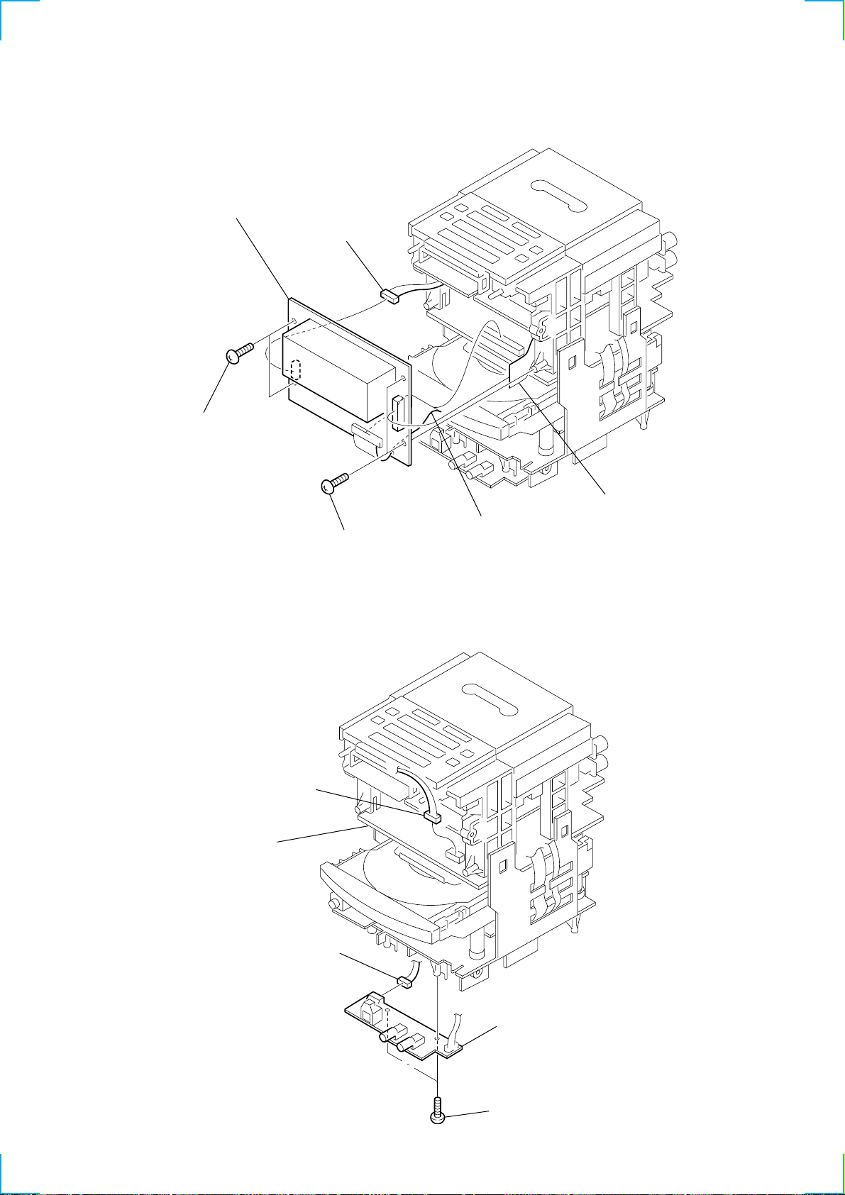
3-9. CD ASSY, H/P BOARD
7 BVTP 3x10
8 H/P board
6 plate, CD
3 CD assy
5 CNP70
4 CNP702
1 BVTP 3x10
2 BVTP 3x10
– 11 –
Page 12
3-10. MAIN BOARD
4
k
5 CNP31
3 MAIN board
4 CNP302
2 BVTP 3x10
3-11. TAPE MECHANISM BLOCK (TC BOARD)
2 BVTP 3x10
1 BVTP 3x10
3 tape mechanism bloc
1 BVTP 3x10
4 CN301
7 BVTP 3x10
– 12 –
8 holder MD
6 TC board
5 BVTP 3x10
Page 13
3-12. T OP BOARD
8
3 panel assy, top
6 TOP board
5 BTP 2.8x8
3-13. “PLATE ASSY, CHUCK”, TRA Y
4 BTP 2.8x8
1 BVTP 3x10
2 BVTP 3x10
2 plate assy, chuck
1 P 2.6x
4 claw
6
3
5 claw
7 tray
– 13 –
Page 14
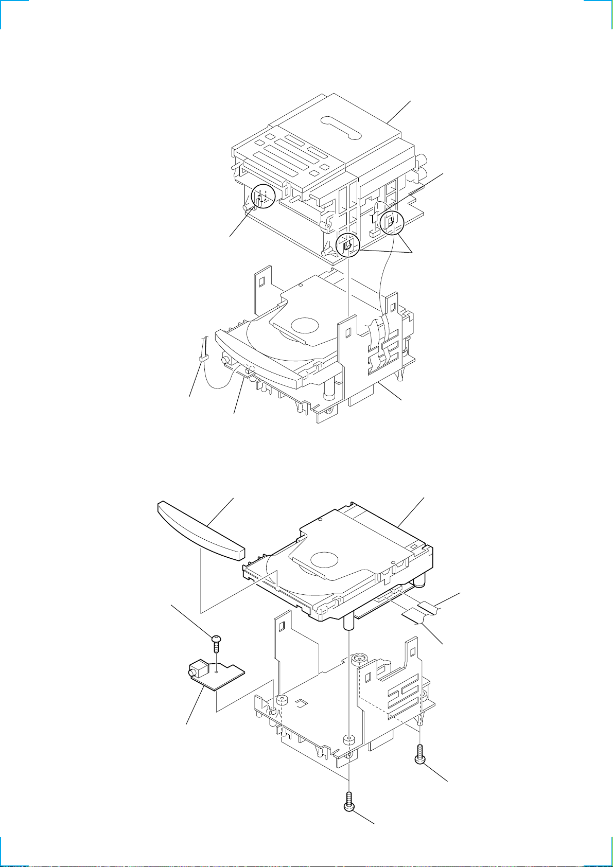
3-14. LOADING BOARD
3 pulley
1 belt
5 B 2x3
4 CN651
6 claw
3-15. CD BOARD
2 claw
7 claw
8 LOADING board
3 CNP701
4 CD board
1 Removal the
four solders.
2 P 2x5
– 14 –
Page 15
k
3-16. CD MECHANISM BLOCK
9
1 PWH 2.6x10
2 gear, drive
3 gear
0 arm
4 PWH 2.6x10
qa CD mechanism bloc
7
8 PWH 2.6x10
5
CD mechanism block
chassis
6
chassis
arm
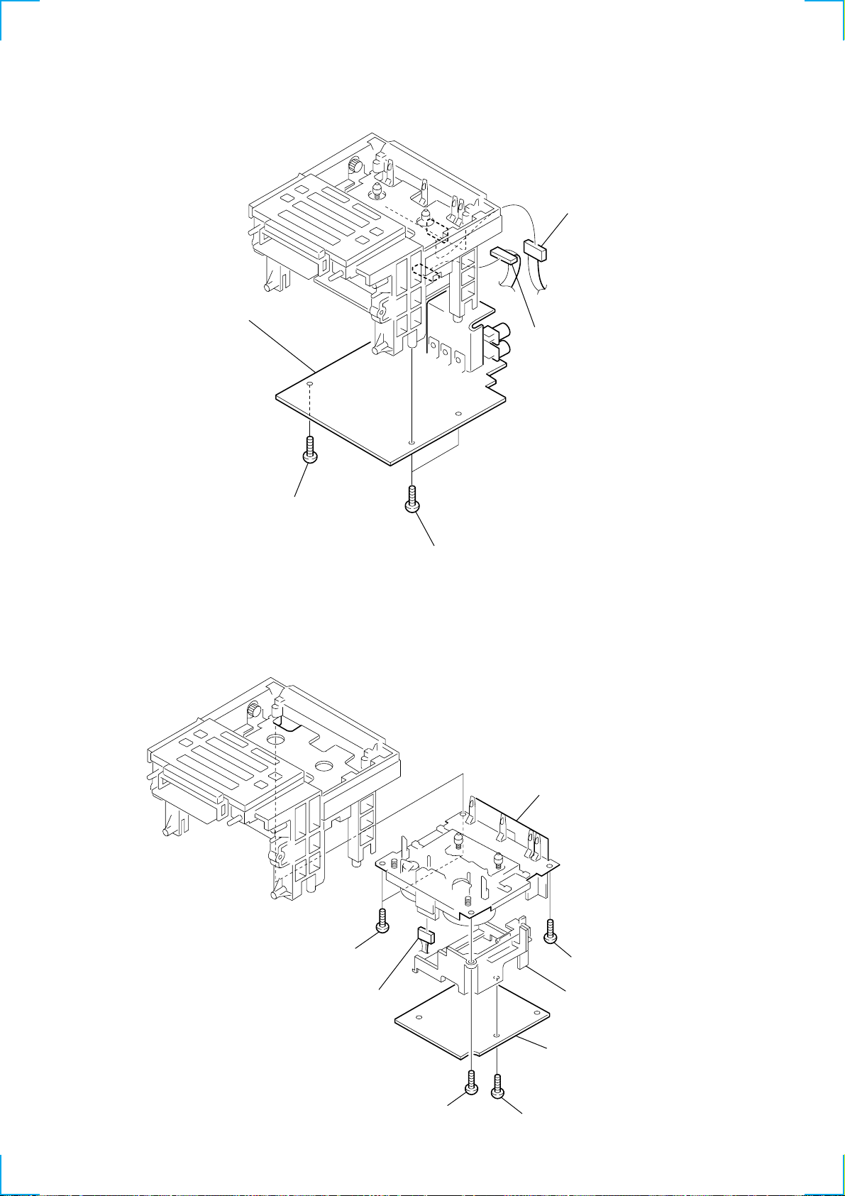
3-17. POWER BOARD
5 CNP903
qs BVTP 3x10
6 CNP911
qd B 4x6
qf power board
7 CNP901
4 bracket, cover
0 speaker board
9 BTP 2.6x8
1 scews +B tapping
8 CNP902
qa BVTP 3x10
2 scews +B tapping
– 15 –
3 cabinet (rear), speaker
Page 16
(
)
y
SECTION 4
MECHANICAL ADJUSTMENTS
SECTION 5
ELECTRICAL ADJUSTMENTS
PRECAUTION
1. Clean the following parts with a denatured-alcohol-moistened
swab:
record/playback/erase head pinch roller
rubber belts capstan
idlers
2. Demagnetize the record/playback/erase head with a head demagnetizer. (Do not bring the head demagnetizer close to the
erase head portion.)
3. Do not use a magnetized screwdriver for the adjustments.
4. After the adjustments, apply suitable locking compound to the
parts adjusted.
5. The adjustments should be performed with the rated power supply voltage unless otherwise noted.
Torque Measurement
Mode Torque Meter Meter Reading
FWD (36 – 61 g•cm)
CQ-102C
FWD
Back tension
REV (36 – 61 g•cm)
CQ-102RC
REV
Back tension
FF, REW CQ-201B (61 – 143 g•cm)
3.53 – 5.98 mN•m
(0.50 – 0.89 oz•inch)
0.20 – 0.58 mN•m
(2.0 – 6.0 g•cm)
(0.028 – 0.076 oz•inch)
3.53 – 5.98 mN•m
(0.50 – 0.89 oz•inch)
0.20 – 0.58 mN•m
(2.0 – 6.0 g•cm)
(0.028 – 0.076 oz•inch)
5.99 – 14.02 mN•m
(0.89 – 2.00 oz•inch)
5-1. TAPE SECTION 0 dB = 0.775 V
1. The adjustments should be performed in the order given in the
service manual. (As a general rule. Playback circuit adjustment
should be completed before performing recording circuit adjustment.)
2. The adjustments should be performed for both L-ch and R-ch
unless otherwise indicated.
Standard Output Level
SP OUT PHONES
Load impedance 4 Ω 32 Ω
Output level 0.775 V (0 dB) 0.25 V (–10 dB)
Test T ape
Type Signal Used for
WS-48B 3 kHz, 0 dB Tape speed adjustment
P-4-A100 10 kHz, –10 dB Head azimuth adjustment
Tape Speed Adjustment
Procedure:
Mode: playback
digital frequenc
test tape
WS-48B
(3 kHz, 0 dB)
set
headphones) jack (J301
i
counter
32 Ω
Tape T ension Measurement
Mode Tension Meter Meter Reading
FWD CQ-403A
REV CQ-403R
(more than 3.52 oz)
more than 100 g
Adjust so that the value on the frequency counter is 3,000 Hz.
Specification Values:
Digital frequency counter
2,970 to 3,030 Hz
Adjust so that the frequency at the beginning and that at the end of
tape winding are between 2,955 and 3,045 Hz.
Adjustment Location:
TC board
M691
TAPE SPEED
Adjustment
– 16 –
Page 17
w
Record/Playback/Erase Head Azimuth Adjustment
Procedure:
1. Mode: FWD/REV playback
test tape
P-4-A100
(10 kHz, –10 dB)
set
i (headphones) jack (J301)
level meter
32 Ω
+
–
2. Turn the adjustment screw for the maximum output levels. If
these levels do not match, turn the adjustment screw
until both
of output levels match together within 1 dB.
Adjustment Location:
screwdriver
FWD
(forward)
REV
(reverse)
L-CH
peak
R-CH
screw
position
peak
3. Phase Check
Mode: FWD/REV playback
test tape
P-4-A100
(10 kHz, –10 dB)
L-CH
set
R-CH
within
1dB
output
level
L-CH
peak
32 Ω
32 Ω
i (headphones) jack (J301)
Screen pattern
R-CH
peak
oscilloscope
V
within
1dB
scre
angle
H
+
+
–
–
in phase 45 ° 90 ° 135 ° 180 °
Good Wrong
4. After the adjustment, lock the screws with locking compound.
– 17 –
Page 18
5-2. TUNER SECTION 0 dB = 1 µV
l
)
• FM Section
Setting:
BAND button: FM
FM RF signal
generator
FM termina
(J1)
0.01 µF
set
75 kHz frequency
deviation by 1 kHz signal
output level : as low as possible
FM FREQUENCY COVERAGE
ADJUSTMENT
Frequency Display 87.5 MHz 108 MHz
Reading on Digital voltmeter 1.5 ± 0.1 V 3.8 ± 0.4 V
Adjustment Part L2 <confirmation>
FM TRACKING ADJUSTMENT
Adjust for a maximum reading on level meter.
L1 CT1
87.5 MHz 108 MHz
• AM Section
Setting:
BAND button: AM
AM RF signal
generator
Put the lead-wire
antenna close to
the AM loop
antenna.
30% amplitude
modulation by 400 Hz signal
output level : as low as possible
• Connecting Level Meter (FM and AM)
level meter
(range: 0.5-5 V ac
32 Ω
set
i (headphones) jack (J301)
• Connecting Digital Voltmeter (FM and AM)
digital
voltmeter
FM IF ADJUSTMENT
Adjust for a maximum reading on level meter.
T2
10.7 MHz (Display: 98 MHz)
AM FREQUENCY COVERAGE
ADJUSTMENT
Frequency Display 530 kHz 1,710 kHz
Reading on Digital voltmeter 0.9 ± 0.1 V 5.1 ± 0.4 V
Adjustment Part T4 <confirmation>
AM TRACKING ADJUSTMENT
Adjust for a maximum reading on level meter.
T3 CT3
620 kHz 1,400 kHz
AM IF ADJUSTMENT
Adjust for a maximum reading on level meter.
T1
450 kHz (Display: 1,000 kHz)
Adjustment Location: TUNER board (See page 19.)
tuner board
TP (VT)
• Repeat the procedures in each adjustment several times, and the
frequency coverage and tracking adjustments should be finally
done by the trimmer capacitors.
– 18 –
Page 19
Adjustment Location:
)
– TUNER BOARD (COMPONENT SIDE) –
TM1
FM
TERMINAL
T1
AM IF
ADJUSTMENT
FM TRACKING
ADJUSTMENT
CT1 L1
AM TRACKING
ADJUSTMENT
T3 CT3
TP(VT)
(conductor side
T2
FM IF
ADJUSTMENT
L2
FM
FREQUENCY
COVERAGE
ADJUSTMENT
T4
AM
FREQUENCY
COVERAGE
ADJUSTMENT
– 19 –
Page 20
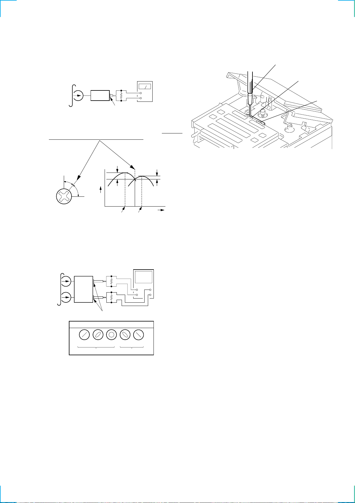
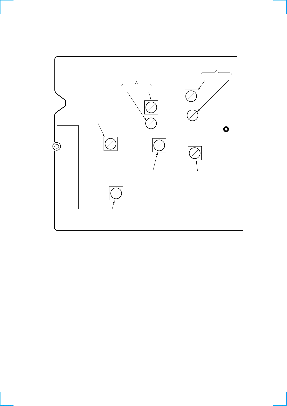
5-3. CD SECTION
Focus Bias Check
This check is to be done when the optical block replaced.
Check Procedure:
1. Connect the oscilloscope to test point TP (RF) on CD board.
Insert disk (YEDS-18 (3-702-101-01)).
2. Press the u button.
3. Check that the oscilloscope waveform is as shown in the figure
below (eye pattern).
A good eye pattern means that the diamond shape ( ) in the
center of the waveform can be clearly distinguished.
4. Release test mode after adjustment is completed.
• RF signal reference waveform (eye pattern)
VOLT/DIV : 50mV
TIME/DIV : 500 ns
(With the 10:1 probe in use)
1.1- 1.3 Vp-p
When observing the eye pattern, set the oscilloscope for AC range
and raise vertical sensitivity.
Adjustment Location: CD board
–CD BOARD (CONDUCTOR SIDE) –
IC702
IC701
TP(RF)
– 20 –
Page 21
SECTION 6
DIAGRAMS
6-1. IC PIN DESCRIPTIONS
• CONTROL BOARD IC801 CXP82832-028Q (SYSTEM CONTROL)
Pin No. Pin Name I/O Pin Description
1 G2 O GRID2 signal output
2 G1 O GRID1 signal output
3NC— Not used. (Fixed at “H”.)
4 C-SCOR I SCOR signal input from the IC702 (CXD2587Q)
5 T-CNT (END) I T-COUNTER (T-END) signal input
6 REG.CHK I P-DOWN IN (B/UP) signal input
7 T-AMS I TAPE AMS IN signal input
8 RMC I Remote control signal input
9 T-MODE I T-MODE SW signal input
10 V-DA/LT O Serial data/latch signal output to the IC302 (BD3859FV)
11 R-CE O R-CE signal output
12 V-CLK O Serial clock signal output to the IC302 (BD3859FV)
13 R-CLK O R-CLOCK signal output
14 R-DATA O R-DATA signal output
15 R-COUNT I R-COUNT signal input
16 C-XLAT O Serial latch signal output to the IC702 (CXD2587Q)
17 C-CLK O Serial clock signal output to the IC702 (CXD2587Q)
18 C-DATA O Serial data signal output to the IC702 (CXD2587Q)
19 C-OPEN.I I CD open switch signal input
20 C-CLOSE.I I CD close switch signal input
21 C-SCLK O SCLK signal output to the IC702 (CXD2587Q)
22 RDS-CLK I Serial clock signal input (Not used in this set.)
23 RDS-DATA I Serial data signal input (Not used in this set.)
24 SD I LR signal detector terminal
25 C-SQCK I SUBQ clock signal input from the IC702 (CXD2587Q)
26 C-SQSO I SUBQ data signal input from the IC702 (CXD2587Q)
27 C-SENS I Sens signal input from the IC702 (CXD2587Q)
28 AVREF — A/D converter Vref pin
29 KEY1 I Key signal input 1
30 KEY2 I Key signal input 2
31 KEY3 I Key signal input 3
32 – 34 F-CD I CD test mode pin
35 T-STAT I/O Tape status signal input/output
36 VERSION I Version read signal input
37 AVSS — Ground
38 RST I Reset signal input from the IC802 (PST9128-T)
39 EXTAL I Clock oscillation input (8 MHz)
40 X’TAL O Clock oscillation output (8 MHz)
41 GND — Ground
42 TX O Crystal connection for clock oscillation (32.768 kHz)
43 TEX I Crystal connection for clock oscillation (32.768 kHz)
44 VDD — Power supply pin
45 VFDP — Voltage for FDP
46 NC — Not used. (Open)
47 C-OPEN.O O CD open signal output
48 C-CLS.O O CD close signal output
49 SFT-CLK O Shift clock signal output
50 C-RST O Reset signal output to the IC702 (CXD2587Q)
– 21 –
Page 22

Pin No. Pin Name I/O Pin Description
51 A-MUTE O System mute signal output
52 B-MUTE O Tuner mute signal output
53 C-MUTE O CD mute signal output
54 LINE-MUTE O Line out mute signal output
55 C-AGCCNT O CD AGC control signal output
56 T-REC O Tape REC signal output
57 T-BIAS O Tape bias signal output
58 T-SOL. O Tape solenoid signal output
59 T-MTR O Tape motor signal output
60 ISS1 O ISS1 signal output
61 ISS2 O ISS2 signal output
62 PWR-SAVE O Power save signal output
63 P-CON O Power control signal output
64 T-AMS.MUTE O Not used. (Open) Tape AMS mute signal output
65 LINE O Not used. (Open) Line out signal output
66 RDS-ON O RDS on signal output (Not used in this set.)
67 TAPE O Tape function signal output
68 TU O Tuner function signal output
69 CD O CD function signal output
70, 71 NC — Not used. (Open)
72 – 87 SEG16-1 O Segment signal output
88 NC — Not used. (Open)
89 VDD — Power supply pin
90 NC — Not used. (Open)
91 G12 O GRID 12 signal output
92 G11 O GRID 11 signal output
93 G10 O GRID 10 signal output
94 G9 O GRID 9 signal output
95 G8 O GRID 8 signal output
96 G7 O GRID 7 signal output
97 G6 O GRID 6 signal output
98 G5 O GRID 5 signal output
99 G4 O GRID 4 signal output
100 G3 O GRID 3 signal output
– 22 –
Page 23

6-2. CIRCUIT BOARDS LOCATION
– Main Section –
HEAD RELAY board
CONTROL board
FRONT board
LOADING board
H/P board
TOP board
LINE board
TC RF board
TC board
MAIN board
TUNER board
CD board
– Speaker (L) Section –
SPEAKER board
POWER board
– 23 – – 24 –
Page 24

PMC-DR45
6-3. BLOCK DIAGRAM — TUNER SECTION —
-1
AM
AM
LOOP
ANTENNA
-2
EXT ANT
TM1
04
TUNER BOARD
BPF
CT3
TRACKING
D3
AM
FERRITE-ROD
ANTENNA
CT3,T3
AM
CT1,L1
FM
TRACKING
T4
AM
FREQUENCY
COVERAGE
T3
RA6V
1182 3 4
CEDICL
DO
LP-OUT
L4
RA6V
AM OSC
AM
OSC
AM
RF-IN
FM
RF-IN
FM
RF-OUT
AM
MIX
D4 D5
22 4 6
2
FM
MIX
FM
OSC
2124
AM IN
11 12
1920
FM OSC
RA6VRA6V
FM IN
FM/AM FRONT-END, IF DET,
FM STEREO DEMODULATOR
OSC-OUT
MIX-OUT
L2L1 CT1
FREQUENCY
COVERAGE
XOUT
20 19
T1
CF2,3
L2
FM
IC1
PLL
IC2
XIN
75kHz
RA6V
X1
RA6V
CF4
T1
AM IF
MO/ST10IF IN
13
14 17 13 18
LPF2/MO-ST
AM
IF-IN
FM
IF-IN
7
BUFFER
IF
IF-OUT
IF CUT
DET
DET
RA6V
AM
FM
10
BAND8ST-IND
7
LPF1/BAND
BUFFER
QUAD
T2
ST-IND
AF
T2
FM IF
DET-OUT
16 15
MPX-IN
FM
MPX
IF CUT
MUTE
R-OUT
L-OUT
MAIN
BOARD
CONTROL BOARD (1/3)
(1/3)
SYSTEM
CONTROL
CNP305
CNP1
(1/2)
R-CE
7
R-DATA
8
R-CLK
9
R-CONT
10
B-MUTE
11
CNP1
RA6V
R-CLK
(2/2)
L CH
6
5
RADIO 6V
11
R-CH
12
CNP307
(1/2)
(1/3)
7
8
9
10
11
1
27
28
29
30
31
TAPE
SECTION
CNP801
(1/3)
5
4
3
2
1
R-CE
R-DATA
R-CLK
R-CNT/ST
B-MUTE
(Page 29)
IC801(1/3)
11
R-CE
14
R-DATA
13
R-CLK
15
R-CONT
B-MUTE
52
Signal path
: FM
: AM
R-ch : same as L-ch.
– 25 – – 26 –
Page 25

6-4. BLOCK DIAGRAM — CD SECTION —
PMC-DR45
A
B
C
D
E
F
LD
PD
OPTICAL
PICK-UP
(KSS-213C)
TRACKING
COIL
FOCUS
COIL
VCC
CD BOARD
CNP701
A
12
B
11
C
10
D
13
E
14
F
9
LD
7
PD
5
VC
16
T+
3
T-
2
F+
4
F-
1
LD
DRIVE
Q701
CD+7.5V
10
19
11
12
14
13
•
CD+5V
T+
T-
F+
F-
CD RF
IC701
5
A
6
B
C
8
D
E
11
10 24
F
3
LD
PD
VC
MUTE
INTER-
FACE
INTER-
FACE
RFO
RFI
FE
TE
VCC
AGCCONT
LD ON
RFE
VREF
TFDR
TRDR
FFDR
FRDR
DIGITAL SIGNAL PROCESSOR,
D/A CONVERTER
IC702
CNP703
RFDC
16
17
147
13
CD+5V
20
224
1512
27
20
5
6
2
3
43
RFAC
51
FE
39
TE
41
SE
40
14
XLON
VC
38
42
CE
30
TFDR
TRDR
31
32
FFDR
33
FRDR
LOUT2
AOUT2
AIN2
LOUT1
AOUT1
AIN1
DOUT
XTAI
XTAO
SQSO
SQCK
XRST
SYSM
DATA
XLAT
CLK
SENS
SCLK
SCOR
75
77
76
72
70
71
60
66
67
1
2
3
4
5
6
7
8
9
20
X701
16.934MHz
R CH
LOUT
CD+5V
CD+7.5V
CD+5V
3
2
6
CNP704 CNP312
DOUT
1 3
22
CNP702 CNP803
SQSO
15
SQCK
14
XRST
13
MUTE
12
DATA
11
XLAT
10
CLK
9
SENS
8
SCLK
7
SCOR
6
AGCCONT
5
OPEN-O
4
CLOSE-O
3
OPEN-I
2
CLOSE-I
1
LOUT
CD+5V
CD+7.5V
3
SECTION
(Page 29)
TAPE
LINE BOARD (1/2)
DIN
CD+5V
3
2
1
CONTROL BOARD (2/3)
SQSO
1
SQCK
2
XRST
3
MUTE
4
DATA
5
XLAT
6
CLK
7
SENS
8
SCLK
9
SCOR
10
AGCCONT
11
OPEN-I
12
CLOSE-I
13
OPEN-O
14
CLOSE-O
15
DOUT
5V
26
25
50
53
18
16
17
27
21
4
55
19
20
47
48
C-SQSO
C-SQCK
C-RST
C-MUTE
C-DATA
C-XLAT
C-CLK
C-SENS
C-SCLK
C-SCOR
C-AGCCONT
C-OPEN.I
C-CLOSE.I
C-OPEN.O
C-CLS.O
IC704
OPTICAL
DIGITAL OUT
(CD)
M701
(SLED)
M702
(SPINDLE)
S701
(LIMIT)
SL+
SL-
SP+
SP-
SL+
17 24
SL-
18 23
SP+
15
SP-
16
SLED,SPINDLE MOTOR
DRIVE
IC703
INTER-
FACE
LEVEL
SHIFT
SFDR
SRDR
SPIN
SFDR
28
29
SRDR
25
26
MDP
27
SSTP
SYSTEM CONTROL
IC801(2/3)
• Signal path
: CD
S651
(LOADING IN/OUT DET)
M651
(LOADING)
04
LOADING BOARD
8
7
LOADING MOTOR DRIVE
CLOSE-O
OPEN-O
CLOSE-I
OPEN-I
IC651
VCC
CN651
6
5
2
2
6
4
1
3
CNJ702
6
5
2
4
1
OPEN-I
CLOSE-I
CLOSE-O
OPEN-O
D702-705
R-ch : same as L-ch.
CD+7.5V
– 27 – – 28 –
Page 26

PMC-DR45
6-5. BLOCK DIAGRAM — TAPE SECTION —
TC BOARD
HRPE301
REC/PB/ERASE
HEAD
CNP301CN301
1
HEAD
RELAY
BOARD
1
2
2
3
3
4
4
5
5
6
6
REC/PB
SWITCH
Q302,303
REC/PB
SWITCH
Q304
REC/PB
SWITCH
Q305
L-CH
R-CH
ERASE
NF
NF
ERASE
SWITCH
Q334
REC/PB
SWITCH
Q306
04
LINE BOARD (2/2) MAIN BOARD (2/3)
CNP311
J311
LINE OUT
J312
LINE IN
REC/PB PRE AMP
IC301
L.PO
2
L.NF
3
L.IN
5
L.RO
4
R.RO
9
R.IN
8
R.NF
10
R.PO
11
6
REF
REC
SWITCH
Q307
AUDIO
+7.5V
R-CH
R-CH
T301
BIAS OSC
ISS
SWITCH
Q310,311
(Page 28)
(Page 26)
BIAS
SWITCH
Q308
CONTROL
Q304
BIAS
LINE IN-L
OUT-L
TAAPE
REC
BIAS OSC
Q301
CD
SECTION
TUNER
SECTION
24
20
15
21
TC RF BOARD
S691
(HEAD POSITION)
S692
(HALF DET)
S693
(CrO2)
S694
(FWD ERASE PROOF)
S695
(REV ERASE PROOF)
M691
(CAPSTAN/REEL)
AUDIO
+7.5V
3
1
ROTATION
R-CH
TAPE-SW
AUDIO
+7.5V
TC-BIAS
TC-REC
CD+7.5V
RADIO 6V
DET
PH691
PLUNGER
SOLENOID
PM691
CNP302
LINE-L
TC.O-L
ISS1
ISS2
L-CH
CD+5V
L-CH
CNP314
CNJ304
4
4
5
5
2
2
1
1
CNP303
11
1
10
2
9
3
8
4
7
5
66
1
11
210
4
8
3
9
CN306
3
1
5
CNP305(2/2)
6
5
CNJ314
9
9
5
5
7
7
3
3
2
2
1
1
4
4
88
CD-L
TU-L
PHOTO
MODE
HALF
CrO2
R-FWD
R-REV
SOL
R-CH
R-CH
COM
+5.6V
R-CHR-CH
R-CH
AUDIO
+7.5V
CD+7.5V
CD+5V
RA+6V
TC MTR
+9.5V
MUTE
Q103
MUTE
Q106
TU/TAPE
SWITCH
Q319,320
MUTE
Q101,
102
SOUND AMP
LINE IN-L
7
LINE.O-L
40
37
FR.IN-L
1
TC.IN-L
3
CD.IN-L
5 19
TU.IN-L
1 6
INPUT
TU
ISS
SWITCH
Q332,333
TC CONTROL
SWITCH
Q330
HALF DET
Q329
IC302
OUT-L
OUT-R
V-DAT/LAT
V-CLK
AMS
IC304
OUTPUT
SYSTEM CONTROL,
5
POWER SECTION
(Page 31)
J302
SIGNAL OUT
13 7
16
R-CH
MUTE
Q104
AUDIO
21
VCC
20
PLUNGER
DRIVE
Q331
+7.5V
HEADPHONE
MUTE
SWITCH
Q316,317
AMP
IC303
MUTE
Q105
-1 L
-2 R
R-CH
CNP309
(1/2)
CNJ310 CNP313
R-CH
V+5V
STANDBY
CNP307
(2/3)
21
15
14
12
24
13
16
17
18
20
J321
SIGNAL IN
-1 L
-2 R
CNP902
33
(1/2)
POWER BOARD (1/2)
5
4
3
1
5
4
3
1
H/P BOARD
TC-AMS
V-DA/LT
V-CLK
LINE MUTE
TAPE
A-MUTE
ISS2
4
3
ISS1
6
TC-BIAS
TC-REC
5
TC-COUNT(END)
TC-MODE
TC-STATUS
TC-SOLENOID
POWER AMP
IC311
2
5
STANDBY
SYSTEM CONTROL,
4
POWER SECTION
• Signal path
: FM
: AM
: CD
: TAPE
: LINE
12
14
17
15
(Page 31)
CNP903
J301
2
1
CNP911
2
3
1
4
J901
SPEAKER
SPEAKER
BOARD
OUT R-CH
IMPEDANCE USE4Ω
SP101
SPEAKER
L-CH
SP201
SPEAKER
R-CH
i
• R-ch : same as L-ch.
– 29 – – 30 –
Page 27

CNP801(2/3)
4
TAPE
SECTION
COM
+5.6V
5
TAPE
SECTION
7
38
42
43
39
40
49
69
63
68
59
45
62
8
31
10
12
54
67
51
61
60
57
56
58
35
9
5
6
11
17
20
18
8
19
28
29
26
27
14
15
16
12
7
9
6
13
23
10
24
•
25
23
26
19
9
22
25
7
•
8
6
7
5
2
8
•
9
5
6
2
7
8
•
9
2
1
CONTROL BOARD (3/3)
TOP BOARD FRONT BOARD
MAIN BOARD (3/3)
POWER BOARD (2/2)
87
I
72
1
•
2
•
I
91
100
2
3
2
4
1
4
2
5
2
1
X801
32kHz
X802
8MHz
TC MTR
+9.5V REG
Q328
RELAY+5V
REG
Q335
MOTOR+9V
REG
Q326
Q327
RELAY+5V
FLT
CD+5V
REG
Q314
COM+5.6V
REG
IC305
AUDIO+7.5V
REG
Q325
CD+7.5V
REG
Q321
COM+5V
REG
Q324
TU+7.5V
SWITCH
Q312
H/P AMP
SWITCH
Q318
S801-811
S818-821
S822-833
SIRCS
RECEIVER
IC804
RESET
IC802
RECT
D906-909
FLAC+3.5V
REG
Q910,911
RECT
D901-904
S812-817
KEY1
KEY2
KEY3
RMC
KEY2
KEY3
KEY1
KEY2
RMC
KEY2
KH811
FDP801
FLUORESCENT
INDICATOR
TUBE
D802
RST
TX
TEX
EXTAL
XTAL
SFT-CLK
CD
P-CON
TU
T-MTR
VFDP
PWR-SAVE
KEY1
KEY2
KEY3
RMC
T-AMS
V-DA/LT
V-CLK
LINE MUTE
TAPE
A-MUTE
ISS1
ISS2
T-BIAS
T-REC
T-SOL.
T-STAT
T-MODE
T-CNT(END)
TC-AMS
V-DA/LT
V-CLK
LINE MUTE
TAPE
A-MUTE
ISS1
ISS2
TC-BIAS
TC-REC
TC-SOLENOID
TC-STATUS
TC-MODE
TC-CNT(END)
REG CHK
VOLTAGE
CHECK
Q803
SYSTEM CONTROL
IC801(3/3)
COM
+5.6V
Q802
Q801
CLOCK SHIFT
Q801,802
CNP801(3/3) CNP307(3/3)
CD
P CONTROL
TU
TC MTR
VFDP
AC1,2
PWR SAVE
CD
P
CONTROL
TU
TC MTR
VFDP
AC1,2
PWR SAVE
SEG1
I
SEG16
G1
G12
29
30
CNP802
CNP804
TC MTR
+9.5V
COM
+5.6V
Q313
Q323
Q315
TU+7.5V
+5V
COM
+5V
CD
+7.5V
AUDIO
+7.5V
CD
+5V
POWER
SWITCH
Q322
DC+12V DC+12V
FL-35V
CNP309
(2/2)
CNP902
(2/2)
Q912
Q913
Q906
Q907
Q905
Q904
Q903
Q902
Q901
Q908
Q909
RELAY+5V
P-SAVE
AC1,2
F902
F901
RELAY
+5V
RY901
T901
POWER
TRANSFORMER
LF901
LINE
FILTER
CNP901
(AC IN)
04
TU
6-6. BLOCK DIAGRAM — SYSTEM CONTROL, POWER SECTION —
PMC-DR45
(Page 30)
(Page 30)
– 31 – – 32 –
Page 28

PMC-DR45
6-7. PRINTED WIRING BOARD — TUNER SECTION —
A
B
C
D
1
234567891011
TP(VT)
TM1
-2
EXT ANT
• Semiconductor
Location
Ref. No. Location
D1 B-8
D2 B-8
D3 C-5
D4 B-6
D5 D-6
IC1 E-7
IC2 D-3
E
F
MAIN BOARD
1
CNP305
(Page 45)
THIS NOTE IS COMMON FOR PRINTED WIRING
BOARDS AND SCHEMATIC DIAGRAMS.
(In addition to this, the necessary note is
printed in each block.)
for Schematic Diagram:
• All capacitors are in µF unless otherwise noted. pF: µµF
50 WV or less are not indicated except for electrolytics
and tantalums.
• All resistors are in Ω and 1/4 W or less unless otherwise
specified.
• % : indicates tolerance.
f
•
• C : panel designation.
: internal component.
Note:
The components identified by mark 0 or dotted
line with mark 0 are critical for safety .
Replace only with part
number specified.
Note:
Les composants identifiés par
une marque 0 sont critiques
pour la sécurité.
Ne les remplacer que par une
piéce portant le numéro
spécifié.
• U : B+ Line.
• V : B– Line.
• H : adjustment for repair.
• Voltages are taken with a VOM (Input impedance 10 MΩ).
Voltage variations may be noted due to normal production tolerances.
• Waveforms are taken with a oscilloscope.
Voltage variations may be noted due to normal production tolerances.
• Circled numbers refer to waveforms.
• Signal path.
F : FM
f : AM
L : LINE
E : PB
a : REC
J : CD
c : digital out
11
1-677-166-
for Printed Wiring Boards:
• X : parts extracted from the component side.
• Y : parts extracted from the conductor side.
a
•
• b : Pattern from the side which enables seeing.
Caution:
Pattern face side: Parts on the pattern face side seen from
(Conductor Side) the pattern face are indicated.
Parts face side: Parts on the parts face side seen from
(Component Side) the parts face are indicated.
: Through hole.
(The other layer’s patterns are not indicated.)
(11)
-1
AM
– 33 – – 34 –
Page 29

6-8. SCHEMATIC DIAGRAM — TUNER SECTION — • Refer to page 65 for IC Block Diagrams. Refer to page 33 for Note.
PMC-DR45
• Voltage is dc with respect to ground under no-signal
(detuned) condition.
no mark : FM
( ) : AM
• Wavef orm
1
IC2 w; (X OUT)
(Page 47)
5µsec/div20mV/div
0.9Vp-p
75kHz
– 35 –
– 36 –
Page 30

PMC-DR45
4.8Vp-p
16.9344MHz
6-9. PRINTED WIRING BOARDS — CD SECTION — • Refer to page 34 for Note.
A
B
C
D
1
• Semiconductor
Location
Ref. No. Location
D701 C-10
D702 C-7
D703 D-7
D704 G-8
D705 G-8
IC651 G-3
IC701 F-12
IC702 E-10
IC703 B-8
Q701 G-14
2 3 4 5 6 7 8 9 1011121314
(Page 52) (Page 45)
TP
(VC)
S701
(LIMIT)
E
F
G
H
FX
FY
TP(FE)
(Page 59)
TP(TE)
TP
(RF)
• Wavef orms
1234
20µsec/div2mV/div 20µsec/div2mV/div 0.5µsec/div50mV/div
Approx. 50mVp-p
IC701 qf (FE) IC701 qh (RFO)IC701 qd (TE)
Approx. 50mVp-p
– 37 – – 38 –
1.1-1.3Vp-p
0.2V/div
IC702 yj (XTAO)
50nsec/div
Page 31

6-10. SCHEMATIC DIAGRAM — CD SECTION — • Refer to page 66 for IC Block Diagrams. Refer to page 38 for Waveforms. Refer to page 33 for Note.
PMC-DR45
(Page 47)
(Page 59)
(Page 54)
• Voltage and waveforms are dc with respect to ground
under no-signal (detuned) conditions.
no mark : CD PLA Y
: Impossible to measure
∗
Note:
The components identified by mark 0 or dotted
line with mark 0 are critical for safety .
Replace only with part
number specified.
Note:
Les composants identifiés par
une marque 0 sont critiques
pour la sécurité.
Ne les remplacer que par une
piéce portant le numéro
spécifié.
– 39 – – 40 –
Page 32

PMC-DR45
6-11. PRINTED WIRING BOARD — TC SECTION — • Refer to page 34 for Note.
A
B
C
D
1
HRPE301
REC/PB/ERASE
HEAD
LCH
RCH
ERASE
234567891011
CN301
1
2
3
4
5
6
12 13
• Semiconductor
Location
Ref. No. Location
D301 F-7
D302 F-6
IC301 D-7
Q301 F-5
Q302 E-3
Q303 E-3
Q304 F-5
Q305 G-6
Q306 F-8
Q307 F-6
Q308 G-7
Q309 G-8
Q310 H-5
Q311 H-6
Q334 F-5
(Page 45)
E
F
G
H
1-673-339-
HEAD
RELAY
BOARD
– 41 – – 42 –
Page 33

6-12. SCHEMATIC DIAGRAM — TC SECTION — • Refer to page 67 for IC Block Diagram. Refer to page 33 for Note.
PMC-DR45
(Page 47)
• Wavef orm
1
0.1V/div
• Voltage is dc with respect to ground under no-signal
(detuned) condition.
no mark : REC (TAPE)
( ) : PB (TAPE)
5µsec/div
4Vp-p
19.5µsec
Q301 C (REC)
– 43 – – 44 –
Page 34

PMC-DR45
6-13. PRINTED WIRING BOARDS — MAIN SECTION — • Refer to page 34 for Note.
A
B
C
D
E
F
G
H
I
1
(Page 60)
(Page 51)
(Page 33)
2 3 4 5 6 7 8 9 10 11 12 13
(Page 42) (Page 38)
i
S694
-1
-2
(Page 61)
(FWD ERASE PROOF)
S693
(CrO2)
CNP314
9
S691
(HEAD POSITION)
S692
1
(HALF DET)
R691
S695
(REV ERASE PROOF)
1-673-338-
PH691
PM691
PLUNGER
SOLENOID
M691
CAPSTAN/REEL
MOTOR
• Semiconductor
Location
Ref. No. Location
D311 H-8
D312 E-9
D313 F-8
D315 H-7
D316 G-8
D317 H-6
D318 H-5
D319 H-4
D321 F-10
D322 H-3
D323 H-7
D324 H-7
D325 I-3
D326 F-3
D327 E-3
IC302 F-5
IC303 D-7
IC304 H-4
IC305 H-3
Q101 C-3
Q102 C-3
Q103 C-5
Q104 C-7
Q105 C-8
Q106 D-2
Q201 C-2
Q202 C-3
Q203 C-6
Q204 C-6
Q205 C-8
Q206 D-2
Q312 G-3
Q313 H-3
Q314 F-7
Q315 E-7
Q316 E-2
Q317 D-3
Q318 E-7
Q319 D-3
Q320 F-3
Q321 F-8
Q322 F-9
Q323 E-9
Q324 G-7
Q325 E-8
Q326 F-8
Q327 G-6
Q328 H-6
Q329 H-5
Q330 G-6
Q331 G-5
Q332 D-2
Q333 D-2
Q335 H-7
Q336 G-3
– 45 – – 46 –
Page 35

6-14. SCHEMATIC DIAGRAM — MAIN SECTION — • Refer to page 68 for IC Block Diagrams. Refer to page 33 for Note.
(Page
59)
PMC-DR45
(Page 63)
(Page 44)
(Page 36)
(Page 40)
(Page 53)
– 47 – – 48 –
• Voltage is dc with respect to ground under no-signal
(detuned) condition.
no mark : FM
( ) : PB (TAPE)
< > : REC (TAPE)
[ ] : CD PLAY
Page 36

PMC-DR45
6-15. PRINTED WIRING BOARD — CONTROL SECTION — • Refer to page 34 for Note.
A
B
C
D
1
2345678910111213
• Waveforms
1
2
0.1V/div
50nsec/div0.2V/div
8MHz
IC801 r; (X’TAL)
10µsec/div
32.768kHz
IC801 rd (TEX)
3Vp-p
2.6Vp-p
E
F
G
H
I
– 49 – – 50 –
Page 37

• Refer to page 34 for Note.
PMC-DR45
(Page 55)
1
111213
0
(Page 45)
23456789
1
• Semiconductor
Location
A
B
Ref. No. Location
D802 D-7
D803 D-3
IC801 G-8
IC802 C-9
IC803 C-3
Q801 D-10
Q802 D-10
Q803 H-3
Q811 B-3
Q812 B-4
C
D
(Page 57)
E
F
(Page 38)
G
H
I
– 51 – – 52 –
Page 38

PMC-DR45
6-16. SCHEMATIC DIAGRAM — CONTROL SECTION — • Refer to page 50 for Waveforms. Refer to page 33 for Note.
(Page 48)
PIN FUNCTION
(Page 40)
(Page 58)
(Page 56)
– 53 – – 54 –
• Voltage and waveforms are dc with respect to
ground under no-signal (detuned) conditions.
no mark : FM
( ) : PB (TAPE)
< > : REC (TAPE)
[ ] : CD PLAY
: Impossible to measure
∗
Page 39

6-17. PRINTED WIRING BOARD — FRONT SECTION — • Refer to page 34 for Note. 6-18. SCHEMATIC DIAGRAM — FRONT SECTION — • Refer to page 33 for Note.
PMC-DR45
A
B
C
D
1
234567
(Page 51)
(Page 54)
E
• Voltage is dc with respect to ground under no-signal
(detuned) condition.
no mark : FM
– 55 – – 56 –
Page 40

PMC-DR45
6-19. PRINTED WIRING BOARD — T OP SECTION — • Refer to page 34 for Note. 6-20. SCHEMATIC DIAGRAM — TOP SECTION — • Refer to page 33 for Note.
A
B
C
D
1
234567
(Page 54)
E
F
(Page 51)
– 57 – – 58 –
Page 41

6-21. PRINTED WIRING BOARD — LINE SECTION — • Refer to page 34 for Note.
PMC-DR45
A
B
C
D
1
23456789
(Page 45)
(Page 38)
6-22. SCHEMATIC DIAGRAM — LINE SECTION — • Refer to page 68 for IC Block Diagram. • Refer to page 33 for Note.
(Page 47)
(Page 40)
• Voltage is dc with respect to ground under no-signal
(detuned) condition.
no mark : CD PLA Y
– 59 – – 60 –
Page 42

PMC-DR45
1
A
B
C
D
E
F
G
H
I
J
2345678910
6-23. PRINTED WIRING BOARDS — POWER SECTION — • Refer to page 34 for Note.
• Semiconductor
Location
Ref. No. Location
D901 F-2
D902 F-2
D903 F-3
D904 F-3
D905 C-1
D906 D-2
D907 D-2
D908 C-2
D909 D-2
D910 H-2
D911 H-2
D912 H-3
IC311 F-7
Q901 I-1
Q902 H-3
Q903 I-3
Q904 H-2
Q905 G-2
Q906 I-2
Q907 H-2
Q908 I-2
Q909 I-1
Q910 G-1
Q911 G-1
Q912 H-4
Q913 H-3
(Page 46)
– 61 – – 62 –
Page 43

6-24. SCHEMATIC DIAGRAM — POWER SECTION — • Refer to page 33 for Note.
PMC-DR45
(Page 48)
• Voltage is dc with respect to ground under no-signal
(detuned) condition.
no mark : FM
Note:
The components identified by mark 0 or dotted
line with mark 0 are critical for safety .
Replace only with part
number specified.
Note:
Les composants identifiés par
une marque 0 sont critiques
pour la sécurité.
Ne les remplacer que par une
piéce portant le numéro
spécifié.
– 63 – – 64 –
Page 44

6-25. IC BLOCK DIAGRAMS
IC701 CXA2568M
GND1
FM RF-IN
AM LOW CUT
MIX OUT
VCC2
AF IF-IN
FM IF-IN
GND2
AGC
QUAD
R-OUT
L-OUT
IC1 TA2149N
1
FM RF
2
3
4
5
6
7
8
9
10
11
12
AM IF
FM IF
AGC
MUTE
FM
MIX
AM
MIX
LEVEL
DET
AM
DET
FM
DET
ST/MO
FM/AM
24
VCC
APC PD AMP
24
FM RF-OUT
23
VCC1
AM RF-IN
22
FM
OSC
AM
OSC
BUFF
BUFF
IF BUFF
1/8
AF BUFF
VCO
DIVIDE
DECODE
ST
SW
IF REQ
1/1 OR
1/16
AF
FM OSC
21
AM OSC
20
19
OSC-OUT
ST-IND
18
IF-OUT
17
16
DET-OUT
MPX- IN
15
14
LPF2/MO-ST
13
LPF1/BAND
HOLD
AGCVTH
LD
PD
A
B
C
D
VEE
F
VEE
1
VEE
2
3
4
5
6
7
8
9
VEE
VC
10
VREF
+
–
+
–
+
–
+
–
VC
+
–
+
–
VC
+
–
VC
VEE
VC
VCC
+
–
+
–
RF EQ AMPRF SUMMING AMP
VC
+
–
+
–
APC LD AMP
VCC
+
–
ERROR AMP
FOCUS
+
–
VC
23
22
21
20
19
18
17
16
15
14
VCC
LC/PD
LD ON
HOLD SW
AGCCONT
(50%/30%
OFF)
RF BOT
RFTC
RF 1
RF 0
RFE
FE
IC2 LC72137M-TLM
CE
1
DI
2
CCB
3
4
5
6
7
8
9
10
UNIVERSAL
COUNTER
I/F
DATA SHIFT REGISTER
CL
DO
MUTE
MW/LW
BAND
ST-IND
BAND
IF IN
LATCH
12BITS
PROGRAMMABLE
DIVIDER
UNLOCK
DETECTOR
SWALLOW
COUNTER
1/16,1/17
4BITS
REFERENCE
DIVIDER
PHASE
DETECTOR
CHARGE
PUMP
POWER ON
RESET
1/2
E
11
VC
+
–
TRACKING
ERROR AMP
MUTE
VREF
GND
13
TE
MUTE
VCC
VCC
VCC
SL–
SL+
17 1516
LEVEL SHIFT
SP–
SP+
–
VC
20
XOUT
XIN
19
18
LP-OUT
17
LP-IN
PD
16
VSS
15
14
VDD
MO/ST
13
FM IN
12
AM IN
11
VC BUFFER
VC
12
VC
IC703 BA5974FP
VCC
28 27 26
VCC
INTERFACE
+
VC
+
–
VREF
NC
SPIN
SFDR
25 24 23 22 21 20 19 18
+ –
INTERFACE
F
SRDR
RF
VCC
VEE
CAPS
R
F
F
R
INTERFACE
RF
R
1 2 3 4 5 6 7
FFDR
– 65 – – 66 –
VREFOUT
FRDR
CAP1
TFDR
TRDR
CAP2
GND
VREFIN
VCC
VCC
111098 12 1413
T+
T–
F–
F+
Page 45

IC702 CXD2587Q
LRCK
PCMD
BCK
EMPH
XVDD
XTAI
XTAO
XVSS
AVDD1
AOUT1
AIN1
LOUT1
AVSS1
AVSS2
LOUT2
AIN2
AOUT2
AVDD2
RMUT
LMUT
DOUT
60 59 58 57
DIGITAL
OUT
61
62
63
64
65
66
67
68
69
70
71
72
73
74
75
76
77
78
79
80
D/A
INTERFACE
TIMING
LOGIC
NOISE SHAPER
OVER SAMPLING
DIGITAL FILTER
PWM PWM
3rd ORDER
SERIAL IN
INTERFACE
VDD
VSS
AVDD3
INTERNAL BUS
ERROR
CORRECTOR
16K
RAM
SUBCODE
PROCESSOR
PCO
FILI
FILO
CTLV
AVSS3
RFAC
BIAS
ASYI
ASYO
AVDD0
IGEN
AVSS0
56 55 54 53 51 50 49 43 42 41
DIGITAL
PLL
EFM
DEMODULATOR
SERVO
INTRFACE
SERVO AUTO
SEQUENCER
ASYMMETRY
CORRECTION
48 47 46 45 4452
ADIO
SERVO DSP
FOCUS
SERVO
TRACKING
SERVO
SLED
SERVO
RFDCCETE
OPERATIONAL
AMPLIFIER
ANALOG SWITCH
A/D
CONVERTER
PWM GENERATOR
PWM GENERATOR
CLOCK
GENERATOR
FOCUS PWM
GENERATOR
TRACKING
SLED PWM
GENERATOR
DIGITAL
CLV
MIRR, DFCT,
FOK
DETECTOR
SE
40
FE
39
VC
38
XTSL
37
TES1
36
TEST
35
VSS
34
FRDR
33
FFDR
32
TRDR
31
TFDR
30
SRDR
29
SFDR
28
SSTP
27
MDP
26
LOCK
25
FOK
24
DFCT
23
MIRR
22
COUT
21
CPU
INTERFACE
987654321 10 11 12 13 14 15 16 17 18 19 20
SQSO
SQCK
XRST
SYSM
DATA
XLAT
CLOK
SENS
SCLK
VDD
ATSK
SPOA
SPOB
XLON
WFCK
XUGF
XPCK
GFS
IC301 TA2068N
RADIO
AGC
1
L. PO
L. NF
L. RO
L IN
REF
GND
R. IN
R. RO
R. NF
R. PO
M. NF
NAS AMP1
2
3
4
5
6
7
8
9 17
10
11
12
REF. AMP
NAS AMP2 BUF. AMP A2
MIC AMP1
BUF. AMP A1
–
+
+
–
RADIO
–
+
ON
MUTE
LINE
LINE
TAPE
TAPE
TAPE
TAPE
BUF. AMP B1
+
–
BUF. AMP B2
+
–
MUTE
ON
MUTE
MONITOR AMP1
ON
ALC1
DET
ALC2
MONITOR AMP2
REC AMP1
REC AMP2
LOGIC
VCC
C2PO
SCOR
24
23
22
21
20
19
18
16
15
14
13
LINE IN L
MIC I/EX
TU L
REC
OUT/L
VCC
OUT/R
LINE TU
TU R
TAPE
LINE IN R
MIC
– 67 –
Page 46

IC302 BD3859FV
FR. IN-R
LINE. O-R
LINE. O-L
40 39 38 37 36
FR. IN-L
TRBL-L
35 34 33
TRBL-R
AGC-T
AGC-LVL
BASS-L
BASS-L
BASS-R
BASS-R
32 31 30 29 28 27 26
DBB. BPF-L
DBB. BPF-L
DBB. BPF-L
DBB. BPF-R
25 24
DBB. BPF-R
DBB. BPF-R
23 22 21
DBB. DET
FILTER
VCC
0dB
–31dB
VCC/2 VCC/2
+
1 2 3 4 5 6 7 8 9 10 11 12
TC. IN-L
TC. IN-R
CD. IN-L
TRBL1
TRBL2 BUS2
+
TU. IN-L
–
TU. IN-R
–
VCC/2
VCC/2
CD. IN-R
VCC/2
VCC/2
LIN. IN-L
BUS1
LIN. IN-R
VCC/2
AGC
VREF. FILT
DBB. SW-T
IC304 LA2010
AMP
COMP(1)
0dB
|
–56dB
T. OUT-L
DYNAMIC
BUS1
+
–
13 15
OUT-L
VR. IN-L
0dB
|
–56dB
T. OUT-R
–
VR. IN-R
DYNAMIC
BUS2
+
16 1714
OUT-R
AGND
DGND
18 19 20
A. GND
D. GND
VCC
LOGIC
V-CLK
V-DAT/LAT
1
IN PUT
IC704 GP1F32T
CONSTANT
VOLTAGE
CIRCUITE
LS TYPE
TTL
OUTPUT
ON/OFF
CONTROL
CIRCUIT
RESET
2
DET OUT
PROTECTIVE
CIRCUIT
COMP(2)
HOLD
5
GND
REFERENCE
VOLTAGE
CIRCUITE
6
4
3
NF
TIME
DRIVE
CIRCUIT
ERROR
BUFFER
CIRCUITE
7
OUT PUT
VCC 2
8
3
2
1
GND
D. OUT
5V
G. GND
9
VCC 1
– 68 –
Page 47

NOTE:
• The mechanical parts with no reference
number in the exploded views are not supplied.
• Items marked “*” are not stocked since
they are seldom required for routine service.
Some delay should be anticipated
when ordering these items.
• -XX and -X mean standardized parts, so
they may have some difference from the
original one.
SECTION 7
EXPLODED VIEWS
• Color Indication of Appearance Parts
Example :
KNOB, BALANCE (WHITE) ... (RED)
RR
Parts Color Cabinet’s Color
• Accessories and packing materials and
hardware (# mark) list are given in
the last of this parts list.
The components identified by
mark 0 or dotted line with mark
0 are critical for safety.
Replace only with part number
specified.
Les composants identifiés par une
marque 0 sont critiques pour
la sécurité.
Ne les remplacer que par une piéce
portant le numéro spécifié.
7-1. CABINET SECTION
9
8
7
6
4
5
10
#1
#2
#1
#1
#2
14
#1
13
A
#1
11
12
#3
#1
FLM-DR45-149
#3
#3
#1
20
A
#1
3
#2
15
16
#1
#1
2
19
1
not supplied
3
#1
18
#1
#1
17
#1
Ref. No. Part No. Description Remark
1 X-3378-630-1 CABINET (FRONT) SUB ASSY
2 3-041-365-01 SPRING, LINK
3 3-044-751-01 FOOT (MAIN)
4 3-044-750-01 RUBBER
5 X-3378-541-1 LINK ASSY, COVER
6 3-041-339-11 COVER (B)
7 3-041-338-01 COVER (A)
8 3-041-337-01 WINDOW , ORNAMENT
9 3-041-346-01 BUTTON, POWER
10 3-041-350-01 BUTTON (A)
Ref. No. Part No. Description Remark
11 3-044-293-01 BUTTON, VOLUME
12 3-041-349-01 BUTTON (EJECT), CD
* 13 1-677-031-11 FRONT BOARD
14 3-041-335-11 CABINET (REAR)
* 15 1-792-256-11 CABLE, FLEXIBLE (6P) (MAIN-CD)
* 16 1-792-226-11 CABLE, FFC (15P) (CD-CONT)
* 17 A-3323-552-A TUNER BOARD, COMPLETE
* 18 1-677-028-11 LINE BOARD
* 19 1-677-029-11 H/P BOARD
20 3-041-340-01 PLATE, CD
– 69 –
Page 48

7-2. CABINET (TOP) SECTION
59
58
60
57
56
61
62
63
64
MF-DR45
#9
67
67
51
52
#9
not supplied
66
#10
#9
65
#9
FDP801
#10
not supplied
Ref. No. Part No. Description Remark Ref. No. Part No. Description Remark
51 3-041-336-01 CABINET (TOP)
52 3-041-370-01 SPRING, CASSETTE
* 53 A-3322-764-A MAIN BOARD, COMPLETE
* 54 A-3322-763-A CONTROL BOARD, COMPLETE
* 55 1-792-225-11 CABLE, FFC (31P) (MAIN-CONT)
55
54
#9
#9
53
#9
60 A-3328-895-A LID ASSY, CASSETTE
61 3-041-342-01 HOLDER, CASSETTE
62 3-029-158-01 CATCHER, PUSH
63 3-029-159-01 SPRING, PUSH CATCHER RETURN
64 3-343-248-01 DAMPER (P), SMALL
#9
* 56 1-677-030-11 TOP BOARD
57 3-041-344-01 BUTTON, FUNCTION
58 3-041-345-01 COVER, SNOOZE
59 3-041-356-11 PANEL (TOP)
* 65 A-3322-501-A TC BOARD, COMPLETE
66 3-041-353-01 HOLDER, FLT
67 3-047-612-01 SCREW +2.6X10
FDP801 1-517-955-11 INDICATOR TUBE, FLUORESCENT
– 70 –
Page 49

7-3. CD CHASSIS SECTION
103
not supplied
not supplied
#4
101
102
112
107
114
113
M651
111
115
#6
104
KSM-213CCP
105
107
106
108
107
106
105
109
110
#5
Ref. No. Part No. Description Remark Ref. No. Part No. Description Remark
101 3-028-010-01 TRAY
102 3-028-019-01 PLATE, CHUCK
103 1-452-899-21 MAGNET
104 3-028-011-01 ARM
105 3-910-095-31 RUBBER, VIBRATION PROOF
106 3-931-379-01 RUBBER, VIBRATION PROOF
107 3-921-725-01 SCREW (2.6X10), +PWH
108 3-028-009-11 CHASSIS
* 109 1-792-227-11 CABLE, FFC (16P) (CD-PICK UP)
* 110 A-3322-766-A CD BOARD, COMPLETE
* 111 1-671-072-11 LOADING BOARD
112 3-028-013-01 GEAR, DRIVE
113 3-028-014-01 GEAR
114 3-028-015-01 PULLEY
115 3-933-020-01 BELT
M651 A-3320-538-A MOTOR ASSY, LOADING (LOADING)
– 71 –
Page 50

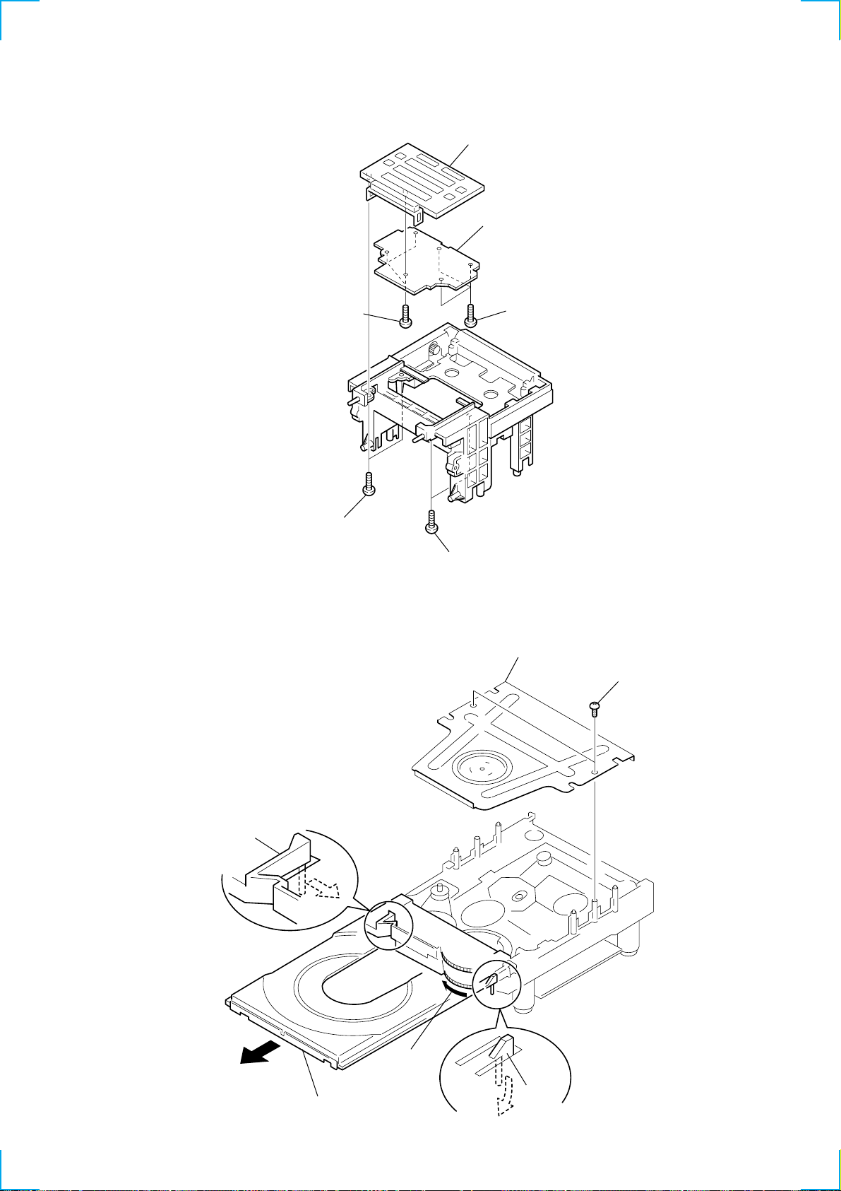
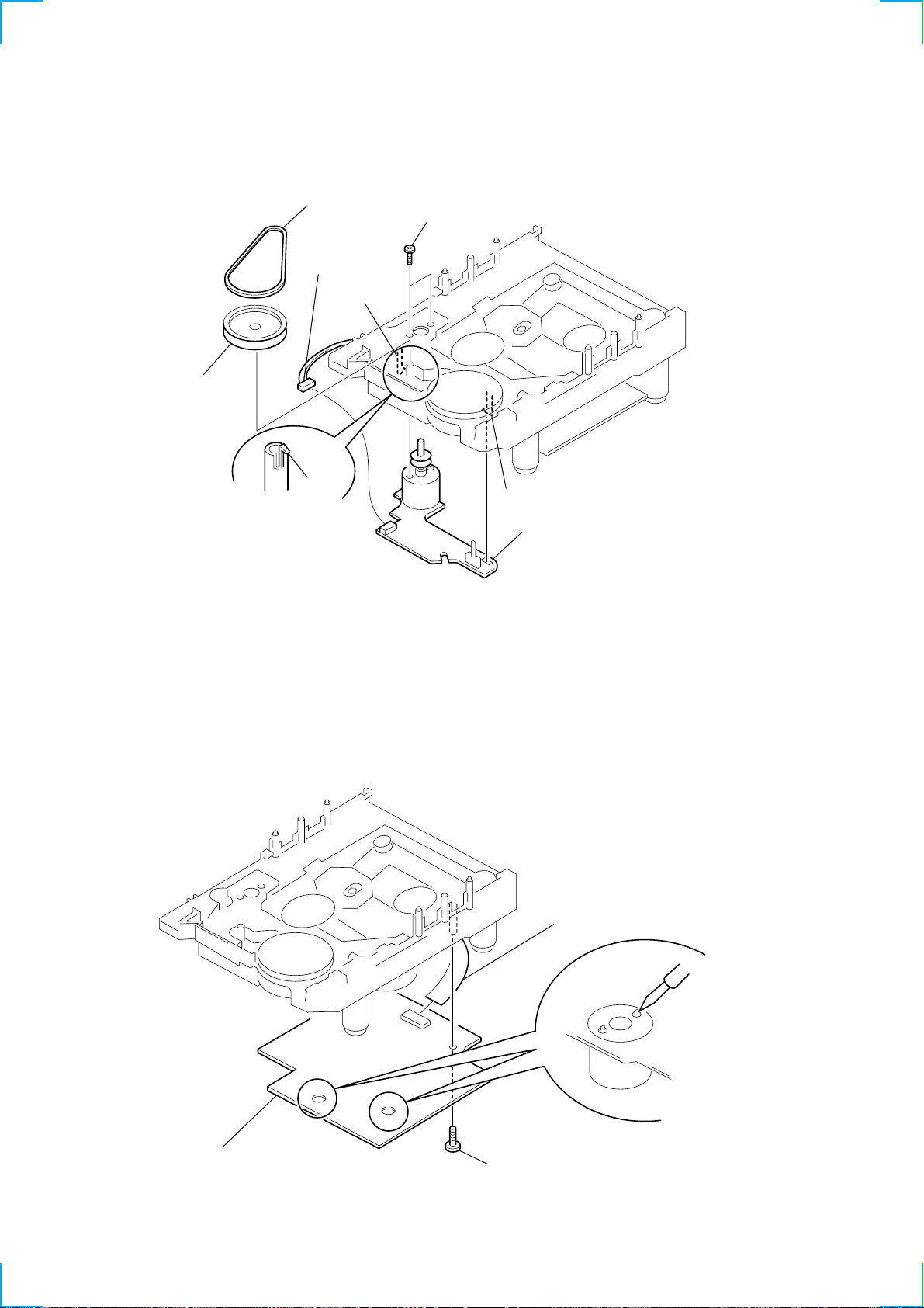
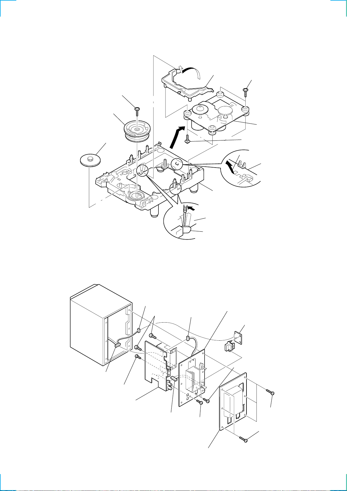
7-4. MECHANISM DECK SECTION (1)
(MF-DR45)
(S692, 693, 694, 695)
182
162
184
165
185
M691
(S692, 693, 694, 695)
183
181
PH691
186
159
158
161
S691
160
173
164
PM691
169
163
175
176
174
178
168
179
177
167
166
180
170
171
172
151
152
157
156
154
153
155
Ref. No. Part No. Description Remark Ref. No. Part No. Description Remark
151 3-043-921-01 SCREW
152 3-029-591-01 COLLAR
153 3-043-906-01 GEAR, CAM
154 3-034-597-01 CAM, ARM
155 3-704-418-14 SCREW (M1.7X4), TAPPING
156 3-043-923-01 WASHER
157 3-029-622-01 WASHER
158 3-043-924-01 WASHER
159 3-029-620-01 WASHER
160 3-029-587-01 COVER
* 161 1-673-338-11 TC RF BOARD
162 3-043-922-01 SCREW
* 163 1-794-105-11 HOUSING
164 3-043-920-01 SCREW
165 3-029-614-01 SCREW
166 3-043-909-01 BELT (FR)
167 3-045-798-01 BELT (SR)
168 3-044-168-01 FLYWHEEL (LA) ASSY
169 3-029-625-01 WASHER
170 3-044-169-01 FLYWHEEL (RA) ASSY
172 3-029-589-01 TRIGGER, ARM
173 3-043-916-01 SPRING
174 3-029-593-01 CLUTCH
175 3-043-917-01 SPRING
176 3-043-911-01 ARM (UD A)
177 3-029-595-01 GEAR (UD)
178 3-043-918-01 SPRING
179 3-043-907-01 PULLEY (D)
180 3-043-926-01 WASHER
181 3-034-694-01 BOX (SW)
182 3-043-910-01 SPRING (SW)
183 3-029-600-01 SPACER
184 3-045-797-01 BRACKET (MOTOR)
185 1-792-511-11 WIRE (MM)
186 3-044-171-01 SOLENOID
M691 3-045-799-01 MOTOR ASSY (CAPSTAN/RELL)
(INCLUDING PULLEY)
PH691 8-719-078-47 PHOTO INTERRUPTER SG-211V
PM691 1-454-896-11 SOLENOID, PLUNGER
S691 1-771-893-11 MODE (SW) (HEAD POSITION)
171 3-029-626-01 WASHER
– 72 –
Page 51

7-5. MECHANISM DECK SECTION (2)
(MF-DR45)
223
224
228
not supplied
226
227
218
219
220
211
221
212
222
216
HRPE301
213
217
225
231
208
214
207
202
232
229
209
215
204
not supplied
230
206
224
223
201
202
203
205
210
Ref. No. Part No. Description Remark Ref. No. Part No. Description Remark
201 3-029-573-01 LEVER (HD)
202 3-029-576-01 PINCH, ROLLER
203 3-029-574-01 PINCH (R), CAP
204 3-029-575-01 PINCH (L), CAP
205 3-043-913-01 SPRING
206 3-029-617-01 SCREW
207 3-043-912-01 SPRING
208 3-029-570-01 FRAME (HD)
209 3-029-611-01 SPRING
210 3-029-616-01 SCREW
211 3-938-941-01 SCREW (A)
212 3-034-598-01 SPRING, AZIMUTH
213 3-029-612-01 SPRING
214 3-043-914-01 SPRING
215 3-029-580-01 LEVER (ST)
216 3-029-614-01 SCREW
* 217 3-044-167-01 PLATE (D) ASSY
218 3-029-578-01 REEL, CAP
219 3-029-602-01 SPRING
220 3-029-579-01 REEL, GEAR
221 3-043-925-01 WASHER
222 3-029-582-01 BRAKE, LEVER
223 3-029-615-01 SCREW
224 3-029-581-01 GUIDE (C)
225 3-029-610-01 SPRING
226 3-029-585-01 ARM (SW)
227 3-029-584-01 ARM (CS)
228 3-043-915-01 SPRING
229 3-029-583-01 FRAME (A)
* 230 1-673-339-11 HEAD RELAY BOARD
231 3-043-905-01 SPRING (AZ)
* 232 1-794-104-11 HOUSING
HRPE301 1-418-847-11 HEAD ASSY, HOLDER (REC/PB/ERASE)
– 73 –
Page 52

7-6. OPTICAL PICK-UP SECTION
(KSM-213CCP)
251
256
not supplied
252
254
253
255
M702
M701
The components identified by
mark 0 or dotted line with mark
0 are critical for safety.
Replace only with part number
specified.
Ref. No. Part No. Description Remark Ref. No. Part No. Description Remark
0 251 8-848-483-05 OPTICAL PICK-UP KSS-213C
252 2-627-003-02 GEAR (B) (RP)
253 2-626-908-01 SHAFT, SLED
254 3-713-786-51 SCREW +P 2X3
255 X-2646-381-1 CHASSIS ASSY (MB) (RP), MOTOR (SPINDLE)
256 2-626-907-01 GEAR (A)
M701 X-2625-769-1 GEAR ASSY, MOTOR (SLED)
Les composants identifiés par une
marque 0 sont critiques pour la
sécurité.
Ne les remplacer que par une piéce
portant le numéro spécifié.
(INCLUDING M702)
– 74 –
Page 53

7-7. SPEAKER (L) SECTION
308
#8
SP101
#8
305
J901
309
306
303
314
312
F901
#7
307
313
F902
#7
T901
#1
310
#3
not supplied
304
310
311
#1
#8
312
302
301
The components identified by
mark 0 or dotted line with mark
0 are critical for safety.
Replace only with part number
specified.
Ref. No. Part No. Description Remark Ref. No. Part No. Description Remark
301 X-3378-631-1 NET ASSY, FRAME
302 3-049-718-01 DUCT (SPEAKER) (L-CH)
303 3-042-254-11 BOX (L), SPEAKER
* 304 A-3322-762-A POWER BOARD, COMPLETE
* 305 1-677-027-11 SPEAKER BOARD
306 3-036-280-01 BUSHING (9 PIN), CORD
307 3-703-244-11 BUSHING (2104), CORD
0 308 1-783-531-11 CORD, POWER
309 3-048-210-01 CUSHION (S.P.K) (B)
310 3-029-171-01 SCREW, +B TAPPING
311 3-041-358-11 CABINET (REAR), SPEAKER
312 3-029-170-01 FOOT (SPEAKER)
313 3-048-209-01 CUSHION (S.P.K) (A)
314 1-757-050-11 LEAD WIRE (WITH CONNECTOR)
0 F901 1-532-501-51 FUSE (0.8A/245V)
0 F902 1-532-506-51 FUSE (6.3A/250V)
J901 1-536-707-21 TERMINAL, PUSH (2P) (SPEAKER OUT R-CH)
SP101 1-529-615-11 SPEAKER (8cm) (L-CH)
0 T901 1-435-351-11 TRANSFORMER, POWER
Les composants identifiés par une
marque 0 sont critiques pour la
sécurité.
Ne les remplacer que par une piéce
portant le numéro spécifié.
– 75 –
Page 54

7-8. SPEAKER (R) SECTION
SP201
#8
#8
353
354
354
352
351
Ref. No. Part No. Description Remark Ref. No. Part No. Description Remark
351 X-3378-631-1 NET ASSY, FRAME
352 3-047-830-01 DUCT (SPEAKER) (R-CH)
353 3-042-255-11 BOX (R), SPEAKER
#8
354 3-029-170-01 FOOT (SPEAKER)
SP201 1-529-615-11 SPEAKER (8cm) (R-CH)
– 76 –
Page 55

SECTION 8
ELECTRICAL PARTS LIST
NOTE:
• Due to standardization, replacements in
the parts list may be different from the
parts specified in the diagrams or the
components used on the set.
• RESISTORS
All resistors are in ohms.
METAL:Metal-film resistor.
METAL OXIDE: Metal oxide-film resistor.
F:nonflammable
Ref. No. Part No. Description Remark Ref. No. Part No. Description Remark
* A-3322-766-A CD BOARD, COMPLETE
*******************
< CAPACITOR >
C701 1-163-009-11 CERAMIC CHIP 0.001uF 10% 50V
C702 1-124-589-11 ELECT 47uF 20% 16V
C703 1-124-584-00 ELECT 100uF 20% 10V
C704 1-163-021-11 CERAMIC CHIP 0.01uF 10% 50V
C705 1-124-584-00 ELECT 100uF 20% 10V
C706 1-163-021-11 CERAMIC CHIP 0.01uF 10% 50V
C707 1-124-584-00 ELECT 100uF 20% 10V
C708 1-163-021-11 CERAMIC CHIP 0.01uF 10% 50V
C709 1-124-234-00 ELECT 22uF 20% 16V
C710 1-163-105-00 CERAMIC CHIP 33PF 5% 50V
C711 1-124-589-11 ELECT 47uF 20% 16V
C712 1-163-021-11 CERAMIC CHIP 0.01uF 10% 50V
C713 1-163-005-11 CERAMIC CHIP 470PF 10% 50V
C714 1-163-117-00 CERAMIC CHIP 100PF 5% 50V
C715 1-163-117-00 CERAMIC CHIP 100PF 5% 50V
C716 1-163-021-11 CERAMIC CHIP 0.01uF 10% 50V
C717 1-163-021-11 CERAMIC CHIP 0.01uF 10% 50V
C718 1-126-176-11 ELECT 220uF 20% 10V
C719 1-163-037-11 CERAMIC CHIP 0.022uF 10% 25V
C720 1-163-001-11 CERAMIC CHIP 220PF 10% 50V
• Items marked “*” are not stocked since
they are seldom required for routine service.
Some delay should be anticipated
when ordering these items.
• SEMICONDUCTORS
In each case, u : µ, for example:
uA.. : µA.. uPA.. : µPA..
uPB.. : µPB.. uPC.. : µPC.. uPD.. : µPD..
• CAPACITORS
uF : µF
• COILS
uH : µH
C743 1-163-121-00 CERAMIC CHIP 150PF 5% 50V
C744 1-163-137-00 CERAMIC CHIP 680PF 5% 50V
C745 1-163-121-00 CERAMIC CHIP 150PF 5% 50V
C746 1-163-137-00 CERAMIC CHIP 680PF 5% 50V
C747 1-163-021-11 CERAMIC CHIP 0.01uF 10% 50V
C749 1-163-117-00 CERAMIC CHIP 100PF 5% 50V
C750 1-163-117-00 CERAMIC CHIP 100PF 5% 50V
C751 1-163-005-11 CERAMIC CHIP 470PF 10% 50V
C752 1-163-117-00 CERAMIC CHIP 100PF 5% 50V
C753 1-163-117-00 CERAMIC CHIP 100PF 5% 50V
C754 1-164-004-11 CERAMIC CHIP 0.1uF 10% 25V
C755 1-163-117-00 CERAMIC CHIP 100PF 5% 50V
C756 1-163-117-00 CERAMIC CHIP 100PF 5% 50V
C757 1-163-117-00 CERAMIC CHIP 100PF 5% 50V
C758 1-163-117-00 CERAMIC CHIP 100PF 5% 50V
C760 1-126-163-11 ELECT 4.7uF 20% 50V
C761 1-126-163-11 ELECT 4.7uF 20% 50V
C762 1-124-584-00 ELECT 100uF 20% 10V
C763 1-163-017-00 CERAMIC CHIP 0.0047uF 5% 50V
C765 1-163-009-11 CERAMIC CHIP 0.001uF 10% 50V
C766 1-124-261-00 ELECT 10uF 20% 50V
C767 1-163-021-11 CERAMIC CHIP 0.01uF 10% 50V
The components identified by
mark 0 or dotted line with mark
0 are critical for safety.
Replace only with part number
specified.
Les composants identifiés par une
marque 0 sont critiques pour
la sécurité.
Ne les remplacer que par une piéce
portant le numéro spécifié.
When indicating parts by reference
number, please include the board.
< CONNECTOR >
CD
C721 1-164-004-11 CERAMIC CHIP 0.1uF 10% 25V
C722 1-163-001-11 CERAMIC CHIP 220PF 10% 50V
C723 1-164-004-11 CERAMIC CHIP 0.1uF 10% 25V
C724 1-124-584-00 ELECT 100uF 20% 10V
C725 1-164-161-11 CERAMIC CHIP 0.0022uF 10% 100V
C726 1-124-584-00 ELECT 100uF 20% 10V
C727 1-163-021-11 CERAMIC CHIP 0.01uF 10% 50V
C728 1-164-004-11 CERAMIC CHIP 0.1uF 10% 25V
C729 1-124-465-00 ELECT 0.47uF 20% 50V
C730 1-163-021-11 CERAMIC CHIP 0.01uF 10% 50V
C731 1-163-001-11 CERAMIC CHIP 220PF 10% 50V
C732 1-163-011-11 CERAMIC CHIP 0.0015uF 10% 50V
C733 1-104-760-11 CERAMIC CHIP 0.047uF 10% 50V
C734 1-163-021-11 CERAMIC CHIP 0.01uF 10% 50V
C736 1-163-017-00 CERAMIC CHIP 0.0047uF 5% 50V
C737 1-163-095-00 CERAMIC CHIP 12PF 5% 50V
C738 1-163-103-00 CERAMIC CHIP 27PF 5% 50V
C739 1-164-004-11 CERAMIC CHIP 0.1uF 10% 25V
C740 1-163-117-00 CERAMIC CHIP 100PF 5% 50V
C742 1-163-021-11 CERAMIC CHIP 0.01uF 10% 50V
CNP701 1-770-168-11 CONNECTOR, FFC/FPC 16P
CNP702 1-695-376-21 PIN, CONNECTOR (PC BOARD) 15P
CNP703 1-770-540-31 PIN, CONNECTOR (PC BOARD) 6P
< DIODE >
D701 8-719-988-61 DIODE 1SS355TE-17
D702 8-719-970-02 DIODE 1SR139-400
D703 8-719-970-02 DIODE 1SR139-400
D704 8-719-970-02 DIODE 1SR139-400
D705 8-719-970-02 DIODE 1SR139-400
< FERRITE BEAD >
FB701 1-410-397-21 FERRITE BEAD INDUCTOR 1.1uH
FB702 1-410-397-21 FERRITE BEAD INDUCTOR 1.1uH
< IC >
IC701 8-752-085-50 IC CXA2568M
IC702 8-752-386-85 IC CXD2587Q
IC703 8-759-549-27 IC BA5974FP
– 77 –
Page 56

CD
Ref. No. Part No. Description Remark Ref. No. Part No. Description Remark
< JUMPER RESISTOR >
JR701 1-216-295-00 SHORT 0
JR702 1-216-295-00 SHORT 0
JR703 1-216-295-00 SHORT 0
JR704 1-216-295-00 SHORT 0
JR705 1-216-295-00 SHORT 0
JR706 1-216-295-00 SHORT 0
JR707 1-216-295-00 SHORT 0
JR708 1-216-295-00 SHORT 0
JR709 1-216-295-00 SHORT 0
JR710 1-216-295-00 SHORT 0
JR711 1-216-295-00 SHORT 0
JR712 1-216-295-00 SHORT 0
JR713 1-216-295-00 SHORT 0
JR714 1-216-295-00 SHORT 0
JR715 1-216-295-00 SHORT 0
JR716 1-216-295-00 SHORT 0
JR717 1-216-295-00 SHORT 0
JR718 1-216-295-00 SHORT 0
JR719 1-216-295-00 SHORT 0
JR720 1-216-295-00 SHORT 0
JR721 1-216-295-00 SHORT 0
JR722 1-216-295-00 SHORT 0
JR723 1-216-295-00 SHORT 0
JR724 1-216-295-00 SHORT 0
JR725 1-216-295-00 SHORT 0
JR726 1-216-295-00 SHORT 0
JR727 1-216-295-00 SHORT 0
JR728 1-216-295-00 SHORT 0
JR729 1-216-295-00 SHORT 0
JR730 1-216-295-00 SHORT 0
JR731 1-216-295-00 SHORT 0
JR732 1-216-295-00 SHORT 0
JR733 1-216-295-00 SHORT 0
JR734 1-216-295-00 SHORT 0
JR735 1-216-295-00 SHORT 0
JR752 1-216-295-00 SHORT 0
JR753 1-216-295-00 SHORT 0
JR754 1-216-295-00 SHORT 0
JR755 1-216-295-00 SHORT 0
JR756 1-216-295-00 SHORT 0
JR757 1-216-295-00 SHORT 0
JR758 1-216-295-00 SHORT 0
JR759 1-216-295-00 SHORT 0
JR760 1-216-295-00 SHORT 0
JR761 1-216-295-00 SHORT 0
JR762 1-216-295-00 SHORT 0
JR763 1-216-295-00 SHORT 0
JR764 1-216-295-00 SHORT 0
JR765 1-216-295-00 SHORT 0
JR766 1-216-295-00 SHORT 0
JR767 1-216-295-00 SHORT 0
JR768 1-216-295-00 SHORT 0
JR769 1-216-295-00 SHORT 0
JR770 1-216-295-00 SHORT 0
JR771 1-216-295-00 SHORT 0
JR772 1-216-295-00 SHORT 0
JR773 1-216-295-00 SHORT 0
JR774 1-216-295-00 SHORT 0
JR775 1-216-295-00 SHORT 0
JR776 1-216-295-00 SHORT 0
JR777 1-216-295-00 SHORT 0
JR778 1-216-295-00 SHORT 0
JR779 1-216-295-00 SHORT 0
JR780 1-216-295-00 SHORT 0
JR781 1-216-295-00 SHORT 0
JR782 1-216-295-00 SHORT 0
JR783 1-216-295-00 SHORT 0
JR784 1-216-295-00 SHORT 0
JR786 1-216-295-00 SHORT 0
JR787 1-216-295-00 SHORT 0
JR788 1-216-295-00 SHORT 0
JR736 1-216-295-00 SHORT 0
JR737 1-216-295-00 SHORT 0
JR738 1-216-295-00 SHORT 0
JR739 1-216-295-00 SHORT 0
JR740 1-216-295-00 SHORT 0
JR741 1-216-295-00 SHORT 0
JR742 1-216-295-00 SHORT 0
JR743 1-216-295-00 SHORT 0
JR744 1-216-295-00 SHORT 0
JR745 1-216-295-00 SHORT 0
JR746 1-216-295-00 SHORT 0
JR747 1-216-295-00 SHORT 0
JR748 1-216-295-00 SHORT 0
JR749 1-216-295-00 SHORT 0
JR750 1-216-295-00 SHORT 0
JR751 1-216-295-00 SHORT 0
< COIL >
L701 1-410-188-51 INDUCTOR CHIP 0.47uH
L702 1-414-137-31 INDUCTOR 0.22uH
< TRANSISTOR >
Q701 8-729-903-46 TRANSISTOR 2SB1132-P
< RESISTOR >
R701 1-216-111-00 METAL CHIP 390K 5% 1/10W
R702 1-216-073-00 METAL CHIP 10K 5% 1/10W
R703 1-216-073-00 METAL CHIP 10K 5% 1/10W
R704 1-216-073-00 METAL CHIP 10K 5% 1/10W
R705 1-216-073-00 METAL CHIP 10K 5% 1/10W
R706 1-216-111-00 METAL CHIP 390K 5% 1/10W
R707 1-216-001-00 METAL CHIP 10 5% 1/10W
– 78 –
Page 57

CD CONTROL
Ref. No. Part No. Description Remark Ref. No. Part No. Description Remark
R708 1-216-049-11 RES-CHIP 1K 5% 1/10W
R710 1-216-073-00 METAL CHIP 10K 5% 1/10W
R711 1-216-073-00 METAL CHIP 10K 5% 1/10W
R712 1-216-065-11 RES-CHIP 4.7K 5% 1/10W
R713 1-216-121-11 RES-CHIP 1M 5% 1/10W
R715 1-216-065-11 RES-CHIP 4.7K 5% 1/10W
R716 1-216-065-11 RES-CHIP 4.7K 5% 1/10W
R719 1-216-085-00 METAL CHIP 33K 5% 1/10W
R720 1-216-089-11 RES-CHIP 47K 5% 1/10W
R722 1-216-085-00 METAL CHIP 33K 5% 1/10W
R723 1-216-099-00 METAL CHIP 120K 5% 1/10W
R724 1-216-081-00 METAL CHIP 22K 5% 1/10W
R725 1-216-089-11 RES-CHIP 47K 5% 1/10W
R726 1-216-065-11 RES-CHIP 4.7K 5% 1/10W
R727 1-216-065-11 RES-CHIP 4.7K 5% 1/10W
R728 1-216-085-00 METAL CHIP 33K 5% 1/10W
R729 1-216-073-00 METAL CHIP 10K 5% 1/10W
R730 1-216-097-11 RES-CHIP 100K 5% 1/10W
R731 1-216-121-11 RES-CHIP 1M 5% 1/10W
R732 1-216-073-00 METAL CHIP 10K 5% 1/10W
R733 1-216-061-00 METAL CHIP 3.3K 5% 1/10W
R734 1-216-061-00 METAL CHIP 3.3K 5% 1/10W
R735 1-216-049-11 RES-CHIP 1K 5% 1/10W
R736 1-216-075-00 METAL CHIP 12K 5% 1/10W
R737 1-216-075-00 METAL CHIP 12K 5% 1/10W
R738 1-216-075-00 METAL CHIP 12K 5% 1/10W
R740 1-216-049-11 RES-CHIP 1K 5% 1/10W
R741 1-216-049-11 RES-CHIP 1K 5% 1/10W
R742 1-216-049-11 RES-CHIP 1K 5% 1/10W
R743 1-216-049-11 RES-CHIP 1K 5% 1/10W
R744 1-216-049-11 RES-CHIP 1K 5% 1/10W
R745 1-216-049-11 RES-CHIP 1K 5% 1/10W
R746 1-216-075-00 METAL CHIP 12K 5% 1/10W
R747 1-216-075-00 METAL CHIP 12K 5% 1/10W
R748 1-216-075-00 METAL CHIP 12K 5% 1/10W
R749 1-216-049-11 RES-CHIP 1K 5% 1/10W
R750 1-216-049-11 RES-CHIP 1K 5% 1/10W
R751 1-216-049-11 RES-CHIP 1K 5% 1/10W
R753 1-216-073-00 METAL CHIP 10K 5% 1/10W
< SWITCH >
* A-3322-763-A CONTROL BOARD, COMPLETE
*************************
3-041-353-01 HOLDER, FLT
< CAPACITOR >
C801 1-162-282-31 CERAMIC 100PF 10% 50V
C802 1-162-282-31 CERAMIC 100PF 10% 50V
C804 1-162-294-31 CERAMIC 0.001uF 10% 50V
C805 1-162-282-31 CERAMIC 100PF 10% 50V
C806 1-162-282-31 CERAMIC 100PF 10% 50V
C807 1-162-282-31 CERAMIC 100PF 10% 50V
C808 1-162-282-31 CERAMIC 100PF 10% 50V
C809 1-162-282-31 CERAMIC 100PF 10% 50V
C810 1-162-282-31 CERAMIC 100PF 10% 50V
C811 1-136-169-00 MYLAR 0.22uF 5% 50V
C812 1-136-169-00 MYLAR 0.22uF 5% 50V
C813 1-127-888-21 CERAMIC 0.1uF 10% 50V
C814 1-127-888-21 CERAMIC 0.1uF 10% 50V
C815 1-127-888-21 CERAMIC 0.1uF 10% 50V
C826 1-162-306-11 CERAMIC 0.01uF 20% 16V
C827 1-126-960-11 ELECT 1uF 20% 50V
C828 1-102-516-11 CERAMIC 27PF 5% 50V
C829 1-102-516-11 CERAMIC 27PF 5% 50V
C830 1-102-518-11 CERAMIC 33PF 5% 50V
C831 1-102-518-11 CERAMIC 33PF 5% 50V
C832 1-162-306-11 CERAMIC 0.01uF 20% 16V
C833 1-162-306-11 CERAMIC 0.01uF 20% 16V
C834 1-102-962-00 CERAMIC 30PF 5% 50V
C835 1-102-962-00 CERAMIC 30PF 5% 50V
C838 1-162-294-31 CERAMIC 0.001uF 10% 50V
C839 1-162-282-31 CERAMIC 100PF 10% 50V
C840 1-162-282-31 CERAMIC 100PF 10% 50V
C841 1-162-282-31 CERAMIC 100PF 10% 50V
C843 1-162-294-31 CERAMIC 1000PF 10% 50V
C844 1-162-282-31 CERAMIC 100PF 10% 50V
C845 1-162-282-31 CERAMIC 100PF 10% 50V
C846 1-162-282-31 CERAMIC 100PF 10% 50V
C847 1-162-282-31 CERAMIC 100PF 10% 50V
C848 1-162-282-31 CERAMIC 100PF 10% 50V
C849 1-162-282-31 CERAMIC 100PF 10% 50V
S701 1-762-812-11 SWITCH, LEAF (LIMIT)
< VIBRATOR >
X701 1-767-226-11 VIBRATOR, CRYSTAL (16.9344MHz)
*************************************************************
– 79 –
C850 1-162-282-31 CERAMIC 100PF 10% 50V
C851 1-162-282-31 CERAMIC 100PF 10% 50V
C852 1-162-282-31 CERAMIC 100PF 10% 50V
C854 1-162-282-31 CERAMIC 100PF 10% 50V
C855 1-162-282-31 CERAMIC 100PF 10% 50V
C856 1-162-282-31 CERAMIC 100PF 10% 50V
C857 1-162-282-31 CERAMIC 100PF 10% 50V
C858 1-162-282-31 CERAMIC 100PF 10% 50V
C859 1-162-294-31 CERAMIC 0.001uF 10% 50V
C863 1-162-282-31 CERAMIC 100PF 10% 50V
C864 1-162-282-31 CERAMIC 100PF 10% 50V
C867 1-125-507-11 DOUBLE LAYERS 0.22F 5.5V
Page 58

CONTROL
Ref. No. Part No. Description Remark Ref. No. Part No. Description Remark
C868 1-162-282-31 CERAMIC 100PF 10% 50V
C869 1-104-664-11 ELECT 47uF 20% 10V
C873 1-126-968-11 ELECT 100uF 20% 50V
< CONNECTOR >
R820 1-249-437-11 CARBON 47K 5% 1/4W
R821 1-249-437-11 CARBON 47K 5% 1/4W
R824 1-249-417-11 CARBON 1K 5% 1/4W
R825 1-249-417-11 CARBON 1K 5% 1/4W
R826 1-249-417-11 CARBON 1K 5% 1/4W
CNP801 1-695-392-31 PIN, CONNECTOR (PC BOARD) 31P
CNP802 1-506-987-11 PIN, CONNECTOR (PC BOARD) 5P
CNP803 1-695-338-11 PIN, CONNECTOR (PC BOARD) 15P
* CNP804 1-580-155-11 PIN, CONNECTOR (PC BOARD) 3P
< DIODE >
D802 8-719-991-33 DIODE 1SS133T-77
D803 8-719-991-33 DIODE 1SS133T-77
< FLUORESCENT INDICATOR >
FDP801 1-517-955-11 INDICATOR TUBE, FLUORESCENT
< IC >
IC801 8-752-912-32 IC CXP82832-028Q
IC802 8-759-645-87 IC PST9128-T
< COIL >
L802 1-414-146-31 INDUCTOR 2.2uH
L804 1-410-336-11 INDUCTOR 220uH
L805 1-414-146-31 INDUCTOR 2.2uH
L807 1-408-615-31 INDUCTOR 100uH
L808 1-408-615-31 INDUCTOR 100uH
< TRANSISTOR >
Q801 8-729-036-89 TRANSISTOR KTC3198GR-AT
Q802 8-729-036-89 TRANSISTOR KTC3198GR-AT
Q803 8-729-036-89 TRANSISTOR KTC3198GR-AT
< RESISTOR >
R801 1-249-417-11 CARBON 1K 5% 1/4W
R802 1-249-425-11 CARBON 4.7K 5% 1/4W
R803 1-249-429-11 CARBON 10K 5% 1/4W
R804 1-249-425-11 CARBON 4.7K 5% 1/4W
R805 1-249-417-11 CARBON 1K 5% 1/4W
R806 1-249-425-11 CARBON 4.7K 5% 1/4W
R807 1-249-417-11 CARBON 1K 5% 1/4W
R808 1-249-417-11 CARBON 1K 5% 1/4W
R809 1-249-417-11 CARBON 1K 5% 1/4W
R810 1-249-417-11 CARBON 1K 5% 1/4W
R811 1-249-417-11 CARBON 1K 5% 1/4W
R812 1-249-417-11 CARBON 1K 5% 1/4W
R813 1-249-417-11 CARBON 1K 5% 1/4W
R814 1-249-421-11 CARBON 2.2K 5% 1/4W
R815 1-249-421-11 CARBON 2.2K 5% 1/4W
R816 1-249-421-11 CARBON 2.2K 5% 1/4W
R817 1-249-421-11 CARBON 2.2K 5% 1/4W
R818 1-249-417-11 CARBON 1K 5% 1/4W
R819 1-249-437-11 CARBON 47K 5% 1/4W
R827 1-249-417-11 CARBON 1K 5% 1/4W
R829 1-249-417-11 CARBON 1K 5% 1/4W
R830 1-249-417-11 CARBON 1K 5% 1/4W
R831 1-249-417-11 CARBON 1K 5% 1/4W
R832 1-249-425-11 CARBON 4.7K 5% 1/4W
R833 1-249-425-11 CARBON 4.7K 5% 1/4W
R834 1-249-425-11 CARBON 4.7K 5% 1/4W
R835 1-249-437-11 CARBON 47K 5% 1/4W
R836 1-247-874-11 CARBON 62K 5% 1/4W
R837 1-249-429-11 CARBON 10K 5% 1/4W
R839 1-247-815-11 CARBON 220 5% 1/4W
R840 1-247-887-00 CARBON 220K 5% 1/4W
R841 1-249-425-11 CARBON 4.7K 5% 1/4W
R842 1-249-425-11 CARBON 4.7K 5% 1/4W
R843 1-249-417-11 CARBON 1K 5% 1/4W
R844 1-249-437-11 CARBON 47K 5% 1/4W
R845 1-249-417-11 CARBON 1K 5% 1/4W
R846 1-249-417-11 CARBON 1K 5% 1/4W
R847 1-249-417-11 CARBON 1K 5% 1/4W
R848 1-249-429-11 CARBON 10K 5% 1/4W
R849 1-249-437-11 CARBON 47K 5% 1/4W
R850 1-249-425-11 CARBON 4.7K 5% 1/4W
R851 1-249-425-11 CARBON 4.7K 5% 1/4W
R852 1-249-425-11 CARBON 4.7K 5% 1/4W
R853 1-249-425-11 CARBON 4.7K 5% 1/4W
R854 1-249-425-11 CARBON 4.7K 5% 1/4W
R855 1-249-425-11 CARBON 4.7K 5% 1/4W
R856 1-249-425-11 CARBON 4.7K 5% 1/4W
R857 1-249-417-11 CARBON 1K 5% 1/4W
R858 1-249-417-11 CARBON 1K 5% 1/4W
R859 1-249-421-11 CARBON 2.2K 5% 1/4W
R860 1-249-421-11 CARBON 2.2K 5% 1/4W
R861 1-249-421-11 CARBON 2.2K 5% 1/4W
R862 1-249-417-11 CARBON 1K 5% 1/4W
R863 1-249-417-11 CARBON 1K 5% 1/4W
R866 1-249-417-11 CARBON 1K 5% 1/4W
R867 1-249-417-11 CARBON 1K 5% 1/4W
R868 1-249-417-11 CARBON 1K 5% 1/4W
R869 1-249-417-11 CARBON 1K 5% 1/4W
R871 1-249-429-11 CARBON 10K 5% 1/4W
R872 1-249-437-11 CARBON 47K 5% 1/4W
R873 1-249-401-11 CARBON 47 5% 1/4W
R874 1-249-421-11 CARBON 2.2K 5% 1/4W
R875 1-249-425-11 CARBON 4.7K 5% 1/4W
R876 1-249-425-11 CARBON 4.7K 5% 1/4W
R878 1-247-863-11 CARBON 22K 5% 1/4W
R879 1-247-863-11 CARBON 22K 5% 1/4W
R880 1-247-863-11 CARBON 22K 5% 1/4W
– 80 –
Page 59

FRONTCONTROL H/P LINEHEAD RELAY
Ref. No. Part No. Description Remark Ref. No. Part No. Description Remark
R883 1-249-403-11 CARBON 68 5% 1/4W
< VIBRATOR >
X801 1-767-697-11 VIBRATOR, CRYSTAL (32kHz)
X802 1-781-598-11 VIBRATOR, CERAMIC (8MHz)
*************************************************************
S831 1-762-798-11 SWITCH, KEY BOARD (COUNTER RESET)
S832 1-762-798-11 SWITCH, KEY BOARD (DIR MODE)
S833 1-762-798-11 SWITCH, KEY BOARD (SUMMER TIME)
*************************************************************
* 1-673-339-11 HEAD RELAY BOARD
*****************
* 1-677-031-11 FRONT BOARD
************
< CAPACITOR >
C871 1-162-282-31 CERAMIC 100PF 10% 50V
C872 1-127-888-21 CERAMIC 0.1uF 10% 50V
< IC >
IC804 8-749-016-97 IC NJL62H400A
< CABLE HOLDER >
* KH805 1-565-386-11 HOLDER, CABLE 5P
< RESISTOR >
R401 1-249-413-11 CARBON 470 5% 1/4W
R402 1-249-412-11 CARBON 390 5% 1/4W
R403 1-249-413-11 CARBON 470 5% 1/4W
R404 1-249-413-11 CARBON 470 5% 1/4W
R405 1-249-415-11 CARBON 680 5% 1/4W
R406 1-249-415-11 CARBON 680 5% 1/4W
R407 1-249-417-11 CARBON 1K 5% 1/4W
R408 1-249-418-11 CARBON 1.2K 5% 1/4W
R409 1-249-419-11 CARBON 1.5K 5% 1/4W
R410 1-249-421-11 CARBON 2.2K 5% 1/4W
*************************************************************
* 1-677-029-11 H/P BOARD
**********
< CAPACITOR >
C141 1-162-294-31 CERAMIC 0.001uF 10% 50V
C241 1-162-294-31 CERAMIC 0.001uF 10% 50V
< CONNECTOR >
CNP313 1-506-987-11 PIN, CONNECTOR (PC BOARD) 5P
< JACK >
J301 1-566-891-11 JACK (i)
< COIL >
L101 1-410-509-11 INDUCTOR 10uH
L201 1-410-509-11 INDUCTOR 10uH
L301 1-410-750-41 INDUCTOR 0.47uH
< RESISTOR >
R132 1-249-429-11 CARBON 10K 5% 1/4W
R232 1-249-429-11 CARBON 10K 5% 1/4W
*************************************************************
R411 1-247-843-11 CARBON 3.3K 5% 1/4W
R412 1-249-416-11 CARBON 820 5% 1/4W
R413 1-247-843-11 CARBON 3.3K 5% 1/4W
R414 1-249-418-11 CARBON 1.2K 5% 1/4W
R415 1-249-419-11 CARBON 1.5K 5% 1/4W
R416 1-249-421-11 CARBON 2.2K 5% 1/4W
< SWITCH >
S818 1-762-798-11 SWITCH, KEY BOARD (VOLUME +)
S819 1-762-798-11 SWITCH, KEY BOARD (VOLUME –)
S820 1-762-798-11 SWITCH, KEY BOARD (SOUND)
S821 1-762-798-11 SWITCH, KEY BOARD (MEGA BASS)
S822 1-762-798-11 SWITCH, KEY BOARD (OPERATE)
S823 1-762-798-11 SWITCH, KEY BOARD (STANDBY)
S824 1-762-798-11 SWITCH, KEY BOARD (SLEEP)
S825 1-762-798-11 SWITCH, KEY BOARD (CLOCK)
S826 1-762-798-11 SWITCH, KEY BOARD (TIMER)
S827 1-762-798-11 SWITCH, KEY BOARD (CD OPEN/CLOSE Z)
S828 1-762-798-11 SWITCH, KEY BOARD (DISPLAY)
S829 1-762-798-11 SWITCH, KEY BOARD (MODE MONO/ST ISS)
S830 1-762-798-11 SWITCH, KEY BOARD (ENTER MEMORY)
* 1-677-028-11 LINE BOARD
***********
< CAPACITOR >
C341 1-126-963-11 ELECT 4.7uF 20% 50V
C342 1-161-494-00 CERAMIC 0.022uF 25V
< CONNECTOR >
CNP312 1-695-105-11 PIN, CONNECTOR (PC BOARD) 3P
< DIODE >
D331 8-719-991-33 DIODE 1SS133T-77
D332 8-719-991-33 DIODE 1SS133T-77
< IC >
IC704 8-749-921-12 IC GP1F32T (OPTICAL DIGITAL OUT (CD))
< JACK >
J311 1-566-822-21 JACK (LINE OUT)
J312 1-566-822-21 JACK (LINE IN)
– 81 –
Page 60

LINE LOADING MAIN
Ref. No. Part No. Description Remark Ref. No. Part No. Description Remark
< COIL >
L111 1-414-146-31 INDUCTOR 2.2uH
L112 1-414-146-31 INDUCTOR 2.2uH
L211 1-414-146-31 INDUCTOR 2.2uH
L212 1-414-146-31 INDUCTOR 2.2uH
L311 1-410-750-41 INDUCTOR 0.47uH
L312 1-410-750-41 INDUCTOR 0.47uH
*************************************************************
* 1-671-072-11 LOADING BOARD
**************
< CAPACITOR >
C651 1-104-664-11 ELECT 47uF 20% 10V
< CONNECTOR >
* CN651 1-580-167-11 PIN, CONNECTOR (PC BOARD) 6P
< IC >
IC651 8-759-962-08 IC BA6208
< SWITCH >
S651 1-771-489-11 SWITCH, LEVER SLIDE (LOADING IN/OUT DET)
*************************************************************
C135 1-162-282-31 CERAMIC 100PF 10% 50V
C213 1-127-880-21 CERAMIC 0.022uF 10% 50V
C214 1-126-960-11 ELECT 1uF 20% 50V
C215 1-126-960-11 ELECT 1uF 20% 50V
C216 1-126-960-11 ELECT 1uF 20% 50V
C217 1-126-960-11 ELECT 1uF 20% 50V
C218 1-126-963-11 ELECT 4.7uF 20% 50V
C219 1-126-964-11 ELECT 10uF 20% 50V
C220 1-130-475-00 MYLAR 0.0022uF 5% 50V
C221 1-136-495-11 MYLAR 0.068uF 5% 50V
C222 1-136-495-11 MYLAR 0.068uF 5% 50V
C223 1-136-169-00 MYLAR 0.22uF 5% 50V
C224 1-136-169-00 MYLAR 0.22uF 5% 50V
C225 1-104-665-11 ELECT 100uF 20% 10V
C226 1-126-963-11 ELECT 4.7uF 20% 50V
C227 1-126-960-11 ELECT 1uF 20% 50V
C228 1-162-294-31 CERAMIC 0.001uF 10% 50V
C229 1-104-664-11 ELECT 47uF 20% 10V
C230 1-104-664-11 ELECT 47uF 20% 10V
C231 1-162-282-31 CERAMIC 100PF 10% 50V
C232 1-162-282-31 CERAMIC 100PF 10% 50V
C233 1-162-282-31 CERAMIC 100PF 10% 50V
C234 1-162-282-31 CERAMIC 100PF 10% 50V
C235 1-162-282-31 CERAMIC 100PF 10% 50V
C313 1-127-880-21 CERAMIC 0.022uF 10% 50V
* A-3322-764-A MAIN BOARD, COMPLETE
*********************
7-685-647-79 SCREW +BVTP 3X10 TYPE2 N-S
< CAPACITOR >
C113 1-127-880-21 CERAMIC 0.022uF 10% 50V
C114 1-126-960-11 ELECT 1uF 20% 50V
C115 1-126-960-11 ELECT 1uF 20% 50V
C116 1-126-960-11 ELECT 1uF 20% 50V
C117 1-126-960-11 ELECT 1uF 20% 50V
C118 1-126-963-11 ELECT 4.7uF 20% 50V
C119 1-126-964-11 ELECT 10uF 20% 50V
C120 1-130-475-00 MYLAR 0.0022uF 5% 50V
C121 1-136-495-11 MYLAR 0.068uF 5% 50V
C122 1-136-495-11 MYLAR 0.068uF 5% 50V
C123 1-136-169-00 MYLAR 0.22uF 5% 50V
C124 1-136-169-00 MYLAR 0.22uF 5% 50V
C125 1-104-665-11 ELECT 100uF 20% 10V
C126 1-126-963-11 ELECT 4.7uF 20% 50V
C127 1-126-960-11 ELECT 1uF 20% 50V
C128 1-162-294-31 CERAMIC 0.001uF 10% 50V
C129 1-104-664-11 ELECT 47uF 20% 10V
C130 1-104-664-11 ELECT 47uF 20% 10V
C131 1-162-282-31 CERAMIC 100PF 10% 50V
C132 1-162-282-31 CERAMIC 100PF 10% 50V
C133 1-162-282-31 CERAMIC 100PF 10% 50V
C134 1-162-282-31 CERAMIC 100PF 10% 50V
C314 1-162-292-31 CERAMIC 680PF 10% 50V
C315 1-124-252-00 ELECT 0.33uF 20% 50V
C316 1-126-962-11 ELECT 3.3uF 20% 50V
C317 1-126-961-11 ELECT 2.2uF 20% 50V
C318 1-126-964-11 ELECT 10uF 20% 50V
C319 1-126-963-11 ELECT 4.7uF 20% 50V
C320 1-127-888-21 CERAMIC 0.1uF 10% 50V
C321 1-104-665-11 ELECT 100uF 20% 10V
C322 1-104-664-11 ELECT 47uF 20% 10V
C323 1-127-888-21 CERAMIC 0.1uF 10% 50V
C324 1-162-282-31 CERAMIC 100PF 10% 50V
C325 1-162-282-31 CERAMIC 100PF 10% 50V
C326 1-126-963-11 ELECT 4.7uF 20% 50V
C327 1-126-934-11 ELECT 220uF 20% 10V
C329 1-126-964-11 ELECT 10uF 20% 50V
C351 1-104-665-11 ELECT 100uF 20% 10V
C352 1-161-494-00 CERAMIC 0.022uF 25V
C353 1-126-924-11 ELECT 330uF 20% 10V
C354 1-104-664-11 ELECT 47uF 20% 10V
C355 1-104-665-11 ELECT 100uF 20% 10V
C356 1-162-306-11 CERAMIC 0.01uF 20% 16V
C357 1-104-665-11 ELECT 100uF 20% 10V
C358 1-161-494-00 CERAMIC 0.022uF 25V
C359 1-126-964-11 ELECT 10uF 20% 50V
C360 1-126-382-11 ELECT 100uF 20% 16V
C361 1-104-664-11 ELECT 47uF 20% 10V
C362 1-162-306-11 CERAMIC 0.01uF 20% 16V
C363 1-162-306-11 CERAMIC 0.01uF 20% 16V
– 82 –
Page 61

MAIN
Ref. No. Part No. Description Remark Ref. No. Part No. Description Remark
C364 1-162-306-11 CERAMIC 0.01uF 20% 16V
C365 1-162-306-11 CERAMIC 0.01uF 20% 16V
C366 1-127-888-21 CERAMIC 0.1uF 10% 50V
C367 1-162-306-11 CERAMIC 0.01uF 20% 16V
C368 1-126-963-11 ELECT 4.7uF 20% 50V
Q102 8-729-036-80 TRANSISTOR KRC110M
Q103 8-729-036-77 TRANSISTOR KRC107M
Q104 8-729-905-50 TRANSISTOR DTC343TS
Q105 8-729-036-86 TRANSISTOR KTC3203Y-AT
Q106 8-729-036-80 TRANSISTOR KRC110M
C369 1-104-665-11 ELECT 100uF 20% 10V
C370 1-127-888-21 CERAMIC 0.1uF 10% 50V
C371 1-104-664-11 ELECT 47uF 20% 25V
< CONNECTOR >
* CNP303 1-774-957-11 PIN, CONNECTOR (PC BOARD) 11P
* CNP304 1-580-158-11 PIN, CONNECTOR (PC BOARD) 6P
* CNP305 1-774-957-11 PIN, CONNECTOR (PC BOARD) 11P
* CNP306 1-695-329-31 PIN, CONNECTOR (PC BOARD) 6P
CNP307 1-568-845-11 PIN, CONNECTOR (PC BOARD) 31P
* CNP309 1-770-249-11 HOUSING, CONNECTOR (PC BOARD) 9P
< DIODE >
D311 8-719-991-33 DIODE 1SS133T-77
D312 8-719-991-33 DIODE 1SS133T-77
D313 8-719-110-08 DIODE RD8.2ES-B2
D315 8-719-109-89 DIODE RD5.6ESB2
D316 8-719-110-17 DIODE RD10ESB2
D317 8-719-991-33 DIODE 1SS133T-77
D318 8-719-991-33 DIODE 1SS133T-77
D319 8-719-991-33 DIODE 1SS133T-77
D321 8-719-991-33 DIODE 1SS133T-77
D322 8-719-991-33 DIODE 1SS133T-77
D323 8-719-991-33 DIODE 1SS133T-77
D324 8-719-109-89 DIODE RD5.6ESB2
D325 8-719-991-33 DIODE 1SS133T-77
D326 8-719-991-33 DIODE 1SS133T-77
D327 8-719-991-33 DIODE 1SS133T-77
< IC >
Q201 8-729-036-80 TRANSISTOR KRC110M
Q202 8-729-036-80 TRANSISTOR KRC110M
Q203 8-729-036-77 TRANSISTOR KRC107M
Q204 8-729-905-50 TRANSISTOR DTC343TS
Q205 8-729-036-86 TRANSISTOR KTC3203Y-AT
Q206 8-729-036-80 TRANSISTOR KRC110M
Q312 8-729-037-29 TRANSISTOR KRA102M
Q313 8-729-036-77 TRANSISTOR KRC107M
Q314 8-729-037-13 TRANSISTOR KTA1271Y
Q315 8-729-036-77 TRANSISTOR KRC107M
Q316 8-729-036-77 TRANSISTOR KRC107M
Q317 8-729-037-29 TRANSISTOR KRA102M
Q318 8-729-037-03 TRANSISTOR KTA1266GR-AT
Q319 8-729-037-29 TRANSISTOR KRA102M
Q320 8-729-036-58 TRANSISTOR KRC102M-AT
Q321 8-729-209-15 TRANSISTOR 2SD2012
Q322 8-729-037-03 TRANSISTOR KTA1266GR-AT
Q323 8-729-036-89 TRANSISTOR KTC3198GR-AT
Q324 8-729-036-86 TRANSISTOR KTC3203Y-AT
Q325 8-729-209-15 TRANSISTOR 2SD2012
Q326 8-729-209-15 TRANSISTOR 2SD2012
Q327 8-729-036-58 TRANSISTOR KRC102M-AT
Q328 8-729-037-13 TRANSISTOR KTA1271Y
Q329 8-729-036-77 TRANSISTOR KRC107M
Q330 8-729-036-77 TRANSISTOR KRC107M
Q331 8-729-036-86 TRANSISTOR KTC3203Y-AT
Q332 8-729-037-29 TRANSISTOR KRA102M
Q333 8-729-037-29 TRANSISTOR KRA102M
Q335 8-729-036-86 TRANSISTOR KTC3203Y-AT
Q336 8-729-036-77 TRANSISTOR KRC107M
IC302 8-759-657-36 IC BD3859FV
IC303 8-759-701-54 IC NJM2073D
IC304 8-759-800-71 IC LA2010
IC305 8-759-646-52 IC KIA7805API
< JACK >
J302 1-770-772-11 JACK, PIN 2P (SIGNAL OUTPUT L/R)
< RESISTOR >
JW256 1-249-427-11 CARBON 6.8K 5% 1/4W
JW257 1-249-427-11 CARBON 6.8K 5% 1/4W
< COIL >
L303 1-414-142-11 INDUCTOR 1uH
< TRANSISTOR >
Q101 8-729-036-80 TRANSISTOR KRC110M
< RESISTOR >
R110 1-249-429-11 CARBON 10K 5% 1/4W
R111 1-249-420-11 CARBON 1.8K 5% 1/4W
R114 1-247-807-31 CARBON 100 5% 1/4W
R116 1-249-427-11 CARBON 6.8K 5% 1/4W
R117 1-249-415-11 CARBON 680 5% 1/4W
R118 1-249-417-11 CARBON 1K 5% 1/4W
R119 1-249-417-11 CARBON 1K 5% 1/4W
R120 1-249-437-11 CARBON 47K 5% 1/4W
R121 1-249-431-11 CARBON 15K 5% 1/4W
R122 1-249-441-11 CARBON 100K 5% 1/4W
R123 1-249-429-11 CARBON 10K 5% 1/4W
R124 1-249-421-11 CARBON 2.2K 5% 1/4W
R125 1-247-843-11 CARBON 3.3K 5% 1/4W
R126 1-249-441-11 CARBON 100K 5% 1/4W
R127 1-249-417-11 CARBON 1K 5% 1/4W
R128 1-249-429-11 CARBON 10K 5% 1/4W
– 83 –
Page 62

POWERMAIN
Ref. No. Part No. Description Remark Ref. No. Part No. Description Remark
R129 1-249-425-11 CARBON 4.7K 5% 1/4W
R130 1-249-417-11 CARBON 1K 5% 1/4W
R131 1-247-791-11 CARBON 22 5% 1/4W
R134 1-249-425-11 CARBON 4.7K 5% 1/4W
R210 1-249-429-11 CARBON 10K 5% 1/4W
R362 1-247-815-11 CARBON 220 5% 1/4W
R364 1-249-437-11 CARBON 47K 5% 1/4W
R365 1-249-421-11 CARBON 2.2K 5% 1/4W
R366 1-249-417-11 CARBON 1K 5% 1/4W
R367 1-249-421-11 CARBON 2.2K 5% 1/4W
R211 1-249-420-11 CARBON 1.8K 5% 1/4W
R214 1-247-807-31 CARBON 100 5% 1/4W
R216 1-249-427-11 CARBON 6.8K 5% 1/4W
R217 1-249-415-11 CARBON 680 5% 1/4W
R218 1-249-417-11 CARBON 1K 5% 1/4W
R219 1-249-417-11 CARBON 1K 5% 1/4W
R220 1-249-437-11 CARBON 47K 5% 1/4W
R221 1-249-431-11 CARBON 15K 5% 1/4W
R222 1-249-441-11 CARBON 100K 5% 1/4W
R223 1-249-429-11 CARBON 10K 5% 1/4W
R224 1-249-421-11 CARBON 2.2K 5% 1/4W
R225 1-247-843-11 CARBON 3.3K 5% 1/4W
R226 1-249-441-11 CARBON 100K 5% 1/4W
R227 1-249-417-11 CARBON 1K 5% 1/4W
R228 1-249-429-11 CARBON 10K 5% 1/4W
R229 1-249-425-11 CARBON 4.7K 5% 1/4W
R230 1-249-417-11 CARBON 1K 5% 1/4W
R231 1-247-791-11 CARBON 22 5% 1/4W
R234 1-249-425-11 CARBON 4.7K 5% 1/4W
R320 1-249-426-11 CARBON 5.6K 5% 1/4W
R321 1-247-891-00 CARBON 330K 5% 1/4W
R322 1-249-441-11 CARBON 100K 5% 1/4W
R323 1-249-401-11 CARBON 47 5% 1/4W
R324 1-249-417-11 CARBON 1K 5% 1/4W
R325 1-249-429-11 CARBON 10K 5% 1/4W
R327 1-249-435-11 CARBON 33K 5% 1/4W
R328 1-249-435-11 CARBON 33K 5% 1/4W
R329 1-249-441-11 CARBON 100K 5% 1/4W
R330 1-247-791-11 CARBON 22 5% 1/4W
R331 1-249-425-11 CARBON 4.7K 5% 1/4W
R332 1-249-425-11 CARBON 4.7K 5% 1/4W
R334 1-249-441-11 CARBON 100K 5% 1/4W
R335 1-249-421-11 CARBON 2.2K 5% 1/4W
R336 1-249-421-11 CARBON 2.2K 5% 1/4W
R337 1-249-441-11 CARBON 100K 5% 1/4W
R338 1-249-418-11 CARBON 1.2K 5% 1/4W
R339 1-249-418-11 CARBON 1.2K 5% 1/4W
R340 1-249-429-11 CARBON 10K 5% 1/4W
R351 1-249-413-11 CARBON 470 5% 1/4W
R352 1-247-807-31 CARBON 100 5% 1/4W
R353 1-247-815-11 CARBON 220 5% 1/4W
R354 1-249-434-11 CARBON 27K 5% 1/4W
R356 1-249-429-11 CARBON 10K 5% 1/4W
R357 1-249-421-11 CARBON 2.2K 5% 1/4W
R358 1-249-441-11 CARBON 100K 5% 1/4W
R368 1-247-863-11 CARBON 22K 5% 1/4W
R369 1-249-429-11 CARBON 10K 5% 1/4W
R370 1-249-441-11 CARBON 100K 5% 1/4W
R371 1-249-417-11 CARBON 1K 5% 1/4W
R372 1-249-417-11 CARBON 1K 5% 1/4W
R373 1-249-437-11 CARBON 47K 5% 1/4W
R374 1-249-427-11 CARBON 6.8K 5% 1/4W
R375 1-249-424-11 CARBON 3.9K 5% 1/4W
R376 1-247-815-11 CARBON 220 5% 1/4W
*************************************************************
* A-3322-762-A POWER BOARD, COMPLETE
***********************
1-533-233-31 HOLDER, FUSE
< CAPACITOR >
C181 1-126-957-11 ELECT 0.22uF 20% 50V
C182 1-162-294-31 CERAMIC 0.001uF 10% 50V
C184 1-136-165-00 MYLAR 0.1uF 5% 50V
C185 1-136-165-00 MYLAR 0.1uF 5% 50V
C281 1-126-957-11 ELECT 0.22uF 20% 50V
C282 1-162-294-31 CERAMIC 0.001uF 10% 50V
C284 1-136-165-00 MYLAR 0.1uF 5% 50V
C285 1-136-165-00 MYLAR 0.1uF 5% 50V
C381 1-126-946-11 ELECT 6800uF 20% 25V
C382 1-104-665-11 ELECT 100uF 20% 10V
C384 1-161-494-00 CERAMIC 0.022uF 25V
C385 1-104-664-11 ELECT 47uF 20% 25V
C901 1-136-169-00 MYLAR 0.22uF 5% 50V
C902 1-136-169-00 MYLAR 0.22uF 5% 50V
C903 1-136-169-00 MYLAR 0.22uF 5% 50V
C904 1-136-169-00 MYLAR 0.22uF 5% 50V
C906 1-136-169-00 MYLAR 0.22uF 5% 50V
C907 1-136-169-00 MYLAR 0.22uF 5% 50V
C908 1-136-169-00 MYLAR 0.22uF 5% 50V
C909 1-136-169-00 MYLAR 0.22uF 5% 50V
C910 1-126-968-11 ELECT 100uF 20% 50V
C911 1-127-876-21 CERAMIC 0.01uF 10% 50V
C912 1-127-876-21 CERAMIC 0.01uF 10% 50V
C913 1-127-876-21 CERAMIC 0.01uF 10% 50V
C914 1-126-968-11 ELECT 100uF 20% 50V
C915 1-126-964-11 ELECT 10uF 20% 50V
C916 1-127-880-21 CERAMIC 0.022uF 10% 50V
C917 1-126-960-11 ELECT 1uF 20% 50V
C918 1-126-960-11 ELECT 1uF 20% 50V
R359 1-247-807-31 CARBON 100 5% 1/4W
R360 1-247-807-31 CARBON 100 5% 1/4W
R361 1-247-815-11 CARBON 220 5% 1/4W
< CONNECTOR >
* CNP901 1-793-660-11 PIN, CONNECTOR (PC BOARD) 3P
– 84 –
Page 63

POWER SPEAKER
Ref. No. Part No. Description Remark Ref. No. Part No. Description Remark
* CNP902 1-691-580-11 PIN, CONNECTOR (PC BOARD) 9P
* CNP903 1-564-507-11 PLUG, CONNECTOR 4P
< DIODE >
D901 8-719-046-47 DIODE 1N5401TM
D902 8-719-046-47 DIODE 1N5401TM
D903 8-719-046-47 DIODE 1N5401TM
D904 8-719-046-47 DIODE 1N5401TM
D905 8-719-991-33 DIODE 1SS133T-77
D906 8-719-063-79 DIODE 1N4002B
D907 8-719-063-79 DIODE 1N4002B
D908 8-719-063-79 DIODE 1N4002B
D909 8-719-063-79 DIODE 1N4002B
D910 8-719-991-33 DIODE 1SS133T-77
D911 8-719-109-93 DIODE RD6.2ESB2
D912 8-719-983-38 DIODE MTZJ-T-77-36B
< IC >
R282 1-247-851-11 CARBON 6.8K 5% 1/4W
R283 1-249-385-11 CARBON 2.2 5% 1/6W
R284 1-249-385-11 CARBON 2.2 5% 1/6W
R381 1-249-425-11 CARBON 4.7K 5% 1/4W
R383 1-249-417-11 CARBON 1K 5% 1/4W
R502 1-249-421-11 CARBON 2.2K 5% 1/4W
R503 1-249-421-11 CARBON 2.2K 5% 1/4W
R901 1-249-427-11 CARBON 6.8K 5% 1/4W
R902 1-247-807-31 CARBON 100 5% 1/4W
R903 1-247-739-11 CARBON 100 5% 1/2W
R904 1-247-891-00 CARBON 330K 5% 1/4W
R905 1-247-891-00 CARBON 330K 5% 1/4W
R906 1-249-431-11 CARBON 15K 5% 1/4W
R907 1-249-441-11 CARBON 100K 5% 1/4W
R908 1-247-895-11 CARBON 470K 5% 1/4W
R909 1-249-441-11 CARBON 100K 5% 1/4W
R910 1-247-895-11 CARBON 470K 5% 1/4W
R911 1-249-417-11 CARBON 1K 5% 1/4W
TC
IC311 8-759-333-16 IC LA4705NA
< JACK >
J321 1-770-612-12 JACK, PIN 2P (SIGNAL IN L/R)
< COIL >
L502 1-410-509-11 INDUCTOR 10uH
L503 1-410-509-11 INDUCTOR 10uH
< LINE FILTER >
0 LF901 1-402-663-11 TRANSFORMER, LINE FILTER (LFT)
< TRANSISTOR >
Q901 8-729-036-89 TRANSISTOR KTC3198GR-AT
Q902 8-729-037-34 TRANSISTOR KRA107M
Q903 8-729-036-77 TRANSISTOR KRC107M
Q904 8-729-037-13 TRANSISTOR KTA1271Y
Q905 8-729-036-77 TRANSISTOR KRC107M
Q906 8-729-036-77 TRANSISTOR KRC107M
Q907 8-729-037-34 TRANSISTOR KRA107M
Q908 8-729-036-77 TRANSISTOR KRC107M
Q909 8-729-037-34 TRANSISTOR KRA107M
Q910 8-729-012-83 FET 2SK679A
< RELAY >
0 RY901 1-755-386-11 RELAY
*************************************************************
* 1-677-027-11 SPEAKER BOARD
**************
< CONNECTOR >
* CNP911 1-564-505-11 PLUG, CONNECTOR 2P
< TERMINAL >
J901 1-536-707-21 TERMINAL, PUSH (2P) (SPEAKER OUTPUT
R-CH)
*************************************************************
* A-3322-501-A TC BOARD, COMPLETE
*******************
< CAPACITOR >
C101 1-163-001-11 CERAMIC CHIP 220PF 10% 50V
C103 1-163-139-00 CERAMIC CHIP 820PF 5% 50V
C104 1-104-664-11 ELECT 47uF 20% 10V
C105 1-162-587-11 CERAMIC CHIP 0.039uF 10% 25V
C106 1-164-161-11 CERAMIC CHIP 0.0022uF 10% 100V
Q911 8-729-012-83 FET 2SK679A
Q912 8-729-036-58 TRANSISTOR KRC102M-AT
Q913 8-729-037-34 TRANSISTOR KRA107M
< RESISTOR >
R181 1-249-425-11 CARBON 4.7K 5% 1/4W
R182 1-247-851-11 CARBON 6.8K 5% 1/4W
R183 1-249-385-11 CARBON 2.2 5% 1/6W
R184 1-249-385-11 CARBON 2.2 5% 1/6W
R281 1-249-425-11 CARBON 4.7K 5% 1/4W
– 85 –
C107 1-163-109-00 CERAMIC CHIP 47PF 5% 50V
C108 1-126-959-11 ELECT 0.47uF 20% 50V
C110 1-126-960-11 ELECT 1uF 20% 50V
C111 1-163-001-11 CERAMIC CHIP 220PF 10% 50V
C201 1-163-001-11 CERAMIC CHIP 220PF 10% 50V
C203 1-163-139-00 CERAMIC CHIP 820PF 5% 50V
C204 1-104-664-11 ELECT 47uF 20% 10V
C205 1-162-587-11 CERAMIC CHIP 0.039uF 10% 25V
C206 1-164-161-11 CERAMIC CHIP 0.0022uF 10% 100V
C207 1-163-109-00 CERAMIC CHIP 47PF 5% 50V
The components identified by
mark 0 or dotted line with mark
0 are critical for safety.
Replace only with part number
specified.
Les composants identifiés par une
marque 0 sont critiques pour la
sécurité.
Ne les remplacer que par une piéce
portant le numéro spécifié.
Page 64

TC TC RF
Ref. No. Part No. Description Remark Ref. No. Part No. Description Remark
C208 1-126-959-11 ELECT 0.47uF 20% 50V
C210 1-126-960-11 ELECT 1uF 20% 50V
C211 1-163-001-11 CERAMIC CHIP 220PF 10% 50V
C301 1-104-665-11 ELECT 100uF 20% 10V
C302 1-126-925-11 ELECT 470uF 20% 10V
C303 1-104-665-11 ELECT 100uF 20% 10V
C304 1-163-021-11 CERAMIC CHIP 0.01uF 10% 50V
C305 1-130-485-00 MYLAR 0.015uF 5% 50V
C306 1-163-019-00 CERAMIC CHIP 0.0068uF 10% 50V
C307 1-163-019-00 CERAMIC CHIP 0.0068uF 10% 50V
C308 1-104-664-11 ELECT 47uF 20% 10V
C309 1-163-009-11 CERAMIC CHIP 0.001uF 10% 50V
C310 1-164-161-11 CERAMIC CHIP 0.0022uF 10% 100V
C311 1-163-033-11 CERAMIC CHIP 0.022uF 50V
C312 1-163-033-11 CERAMIC CHIP 0.022uF 50V
C391 1-163-021-11 CERAMIC CHIP 0.01uF 10% 50V
< CONNECTOR >
CNP301 1-580-168-11 PIN, CONNECTOR (PC BOARD) 7P
* CNP302 1-766-594-11 PIN, CONNECTOR (PC BOARD) 11P
Q309 8-729-900-53 TRANSISTOR DTC114EK
Q310 8-729-120-28 TRANSISTOR 2SC1623-L5L6
Q311 8-729-120-28 TRANSISTOR 2SC1623-L5L6
Q334 8-729-120-28 TRANSISTOR 2SC1623-L5L6
< RESISTOR >
R101 1-216-077-11 RES-CHIP 15K 5% 1/10W
R102 1-216-019-00 METAL CHIP 56 5% 1/10W
R103 1-216-097-11 RES-CHIP 100K 5% 1/10W
R104 1-216-061-00 METAL CHIP 3.3K 5% 1/10W
R105 1-216-025-11 RES-CHIP 100 5% 1/10W
R106 1-216-049-11 RES-CHIP 1K 5% 1/10W
R107 1-216-025-11 RES-CHIP 100 5% 1/10W
R108 1-216-033-00 METAL CHIP 220 5% 1/10W
R109 1-216-033-00 METAL CHIP 220 5% 1/10W
R201 1-216-077-11 RES-CHIP 15K 5% 1/10W
R202 1-216-019-00 METAL CHIP 56 5% 1/10W
R203 1-216-097-11 RES-CHIP 100K 5% 1/10W
R204 1-216-061-00 METAL CHIP 3.3K 5% 1/10W
R205 1-216-025-11 RES-CHIP 100 5% 1/10W
R206 1-216-049-11 RES-CHIP 1K 5% 1/10W
< DIODE >
D301 8-719-988-61 DIODE 1SS355TE-17
D302 8-719-988-61 DIODE 1SS355TE-17
< IC >
IC301 8-759-264-71 IC TA2068N
< JUMPER RESISTOR >
JR101 1-216-295-00 SHORT 0
JR102 1-216-295-00 SHORT 0
JR103 1-216-295-00 SHORT 0
JR104 1-216-295-00 SHORT 0
JR105 1-216-295-00 SHORT 0
JR106 1-216-295-00 SHORT 0
JR107 1-216-295-00 SHORT 0
JR108 1-216-295-00 SHORT 0
JR109 1-216-295-00 SHORT 0
JR110 1-216-295-00 SHORT 0
JR111 1-216-295-00 SHORT 0
JR113 1-216-295-00 SHORT 0
JR114 1-216-295-00 SHORT 0
< TRANSISTOR >
Q301 8-729-036-86 TRANSISTOR KTC3203Y-AT
Q302 8-729-120-28 TRANSISTOR 2SC1623-L5L6
Q303 8-729-120-28 TRANSISTOR 2SC1623-L5L6
Q304 8-729-027-23 TRANSISTOR DTA114EKA-T146
Q305 8-729-900-53 TRANSISTOR DTC114EK
Q306 8-729-900-53 TRANSISTOR DTC114EK
Q307 8-729-027-23 TRANSISTOR DTA114EKA-T146
Q308 8-729-027-23 TRANSISTOR DTA114EKA-T146
R207 1-216-025-11 RES-CHIP 100 5% 1/10W
R208 1-216-033-00 METAL CHIP 220 5% 1/10W
R209 1-216-033-00 METAL CHIP 220 5% 1/10W
R301 1-216-121-11 RES-CHIP 1M 5% 1/10W
R302 1-216-017-11 RES-CHIP 47 5% 1/10W
R303 1-216-073-00 METAL CHIP 10K 5% 1/10W
R304 1-216-073-00 METAL CHIP 10K 5% 1/10W
R305 1-216-073-00 METAL CHIP 10K 5% 1/10W
R306 1-216-073-00 METAL CHIP 10K 5% 1/10W
R307 1-216-097-11 RES-CHIP 100K 5% 1/10W
R308 1-216-097-11 RES-CHIP 100K 5% 1/10W
R309 1-216-065-11 RES-CHIP 4.7K 5% 1/10W
R310 1-216-073-00 METAL CHIP 10K 5% 1/10W
R311 1-216-308-00 METAL CHIP 4.7 5% 1/10W
R312 1-216-093-11 RES-CHIP 68K 5% 1/10W
R313 1-216-017-11 RES-CHIP 47 5% 1/10W
R314 1-216-308-00 METAL CHIP 4.7 5% 1/10W
R315 1-216-049-11 RES-CHIP 1K 5% 1/10W
R316 1-216-049-11 RES-CHIP 1K 5% 1/10W
R317 1-216-049-11 RES-CHIP 1K 5% 1/10W
R318 1-216-065-11 RES-CHIP 4.7K 5% 1/10W
< TRANSFORMER >
T301 1-429-820-11 TRANSFORMER, BIAS OSCILLATION
*************************************************************
* 1-673-338-11 TC RF BOARD
***********
< CONNECTOR >
* CNP314 1-580-170-11 PIN, CONNECTOR (PC BOARD) 9P
– 86 –
Page 65

TC RF TOP TUNER
Ref. No. Part No. Description Remark Ref. No. Part No. Description Remark
< PHOTO INTERRUPTER >
PH691 8-719-078-47 PHOTO INTERRUPTER SG-211V
< RESISTOR >
R691 1-249-441-11 CARBON 100K 5% 1/4W
< SWITCH >
S813 1-762-798-11 SWITCH, KEY BOARD (CD u)
S814 1-762-798-11 SWITCH, KEY BOARD (PRESET –)
S815 1-762-798-11 SWITCH, KEY BOARD (BAND AUTO PRESET)
S816 1-762-798-11 SWITCH, KEY BOARD (PRESET +)
S817 1-762-798-11 SWITCH, KEY BOARD (SNOOZE)
*************************************************************
* A-3323-552-A TUNER BOARD, COMPLETE
**********************
S691 1-771-893-11 MODE (SW) (HEAD POSITION)
S692 1-771-661-11 SWITCH, LEAF (HALF DET)
S693 1-771-661-11 SWITCH, LEAF (CrO2)
S694 1-771-661-11 SWITCH, LEAF (FWD ERASE PROOF)
S695 1-771-661-11 SWITCH, LEAF (REV ERASE PROOF)
*************************************************************
* 1-677-030-11 TOP BOARD
**********
< CABLE HOLDER >
* KH811 1-565-384-11 HOLDER, CABLE 3P
< RESISTOR >
R421 1-249-413-11 CARBON 470 5% 1/4W
R422 1-249-412-11 CARBON 390 5% 1/4W
R423 1-249-413-11 CARBON 470 5% 1/4W
R424 1-249-413-11 CARBON 470 5% 1/4W
R425 1-249-415-11 CARBON 680 5% 1/4W
R426 1-249-415-11 CARBON 680 5% 1/4W
R427 1-249-417-11 CARBON 1K 5% 1/4W
R428 1-249-418-11 CARBON 1.2K 5% 1/4W
R429 1-249-419-11 CARBON 1.5K 5% 1/4W
R430 1-249-421-11 CARBON 2.2K 5% 1/4W
R431 1-247-843-11 CARBON 3.3K 5% 1/4W
R432 1-249-413-11 CARBON 470 5% 1/4W
R433 1-249-412-11 CARBON 390 5% 1/4W
R434 1-249-413-11 CARBON 470 5% 1/4W
R435 1-249-413-11 CARBON 470 5% 1/4W
R436 1-249-415-11 CARBON 680 5% 1/4W
R437 1-249-415-11 CARBON 680 5% 1/4W
< SWITCH >
S801 1-762-798-11 SWITCH, KEY BOARD (LINE)
S802 1-762-798-11 SWITCH, KEY BOARD (TAPE N)
S803 1-762-798-11 SWITCH, KEY BOARD (TAPE n)
S804 1-762-798-11 SWITCH, KEY BOARD (TAPE x)
S805 1-762-798-11 SWITCH, KEY BOARD (CD DUBBING)
S806 1-762-798-11 SWITCH, KEY BOARD (z REC)
S807 1-762-798-11 SWITCH, KEY BOARD (m)
S808 1-762-798-11 SWITCH, KEY BOARD (M)
S809 1-762-798-11 SWITCH, KEY BOARD (./TUNING TIME SET –)
S810 1-762-798-11 SWITCH, KEY BOARD (>/TUNING TIME SET +)
S811 1-762-798-11 SWITCH, KEY BOARD (RDS)
S812 1-762-798-11 SWITCH, KEY BOARD (CD x)
< CAPACITOR >
C1 1-163-011-11 CERAMIC CHIP 0.0015uF 10% 50V
C2 1-126-960-11 ELECT 1uF 20% 50V
C3 1-115-339-11 CERAMIC CHIP 0.1uF 10% 50V
C4 1-126-963-11 ELECT 4.7uF 20% 50V
C5 1-163-231-11 CERAMIC CHIP 15PF 5% 50V
C6 1-163-037-00 CERAMIC CHIP 0.022uF 5% 50V
C7 1-163-037-00 CERAMIC CHIP 0.022uF 5% 50V
C8 1-126-934-11 ELECT 220uF 20% 10V
C9 1-163-021-11 CERAMIC CHIP 0.01uF 10% 50V
C10 1-163-037-11 CERAMIC CHIP 0.022uF 10% 25V
C11 1-163-231-11 CERAMIC CHIP 15PF 5% 50V
C12 1-163-129-00 CERAMIC CHIP 330PF 5% 50V
C13 1-115-339-11 CERAMIC CHIP 0.1uF 10% 50V
C14 1-163-009-11 CERAMIC CHIP 0.001uF 10% 50V
C15 1-115-339-11 CERAMIC CHIP 0.1uF 10% 50V
C16 1-163-021-11 CERAMIC CHIP 0.01uF 10% 50V
C17 1-163-021-11 CERAMIC CHIP 0.01uF 10% 50V
C18 1-163-103-11 CERAMIC CHIP 27PF 5% 50V
C19 1-126-960-11 ELECT 1uF 20% 50V
C20 1-163-017-00 CERAMIC CHIP 0.0047uF 5% 50V
C21 1-163-003-11 CERAMIC CHIP 330PF 10% 50V
C22 1-126-960-11 ELECT 1uF 20% 50V
C23 1-115-339-11 CERAMIC CHIP 0.1uF 10% 50V
C24 1-115-339-11 CERAMIC CHIP 0.1uF 10% 50V
C25 1-163-009-11 CERAMIC CHIP 0.001uF 10% 50V
C26 1-163-021-11 CERAMIC CHIP 0.001uF 10% 50V
C27 1-163-021-11 CERAMIC CHIP 0.01uF 10% 50V
C28 1-163-021-11 CERAMIC CHIP 0.01uF 10% 50V
C29 1-163-021-11 CERAMIC CHIP 0.01uF 10% 50V
C30 1-163-227-11 CERAMIC CHIP 10PF 0.5PF 50V
C31 1-163-227-11 CERAMIC CHIP 10PF 0.5PF 50V
C32 1-163-009-11 CERAMIC CHIP 0.001uF 10% 50V
C33 1-104-665-11 ELECT 100uF 20% 10V
C34 1-163-251-11 CERAMIC CHIP 100PF 5% 50V
C35 1-163-009-11 CERAMIC CHIP 0.001uF 10% 50V
C36 1-163-009-11 CERAMIC CHIP 0.001uF 10% 50V
C37 1-163-009-11 CERAMIC CHIP 0.001uF 10% 50V
C38 1-163-009-11 CERAMIC CHIP 0.001uF 10% 50V
C40 1-136-171-00 MYLAR 0.33uF 5% 50V
C41 1-163-021-11 CERAMIC CHIP 0.01uF 10% 50V
C44 1-163-009-11 CERAMIC CHIP 0.001uF 10% 50V
C45 1-163-251-11 CERAMIC CHIP 100PF 5% 50V
C46 1-163-117-00 CERAMIC CHIP 100PF 5% 50V
– 87 –
Page 66

TUNER
Ref. No. Part No. Description Remark Ref. No. Part No. Description Remark
C47 1-163-117-00 CERAMIC CHIP 100PF 5% 50V
C48 1-163-117-00 CERAMIC CHIP 100PF 5% 50V
C49 1-163-117-00 CERAMIC CHIP 100PF 5% 50V
< FILTER >
CF2 1-760-738-61 FILTER, CERAMIC
CF3 1-760-738-61 FILTER, CERAMIC
CF4 1-781-344-12 FILTER, AM CERAMIC
< CONNECTOR >
* CNP1 1-766-594-11 PIN, CONNECTOR (PC BOARD) 11P
< TRIMMER >
CT1 1-141-227-00 TRIMMER, CERAMIC 20PF
CT3 1-141-410-11 CAP, ADJ 10PF
L1 1-416-533-11 COIL, AIR-CORE
L2 1-416-509-11 COIL, AIR-CORE
R1 1-216-073-00 METAL CHIP 10K 5% 1/10W
R2 1-216-037-00 METAL CHIP 330 5% 1/10W
R3 1-216-089-11 RES-CHIP 47K 5% 1/10W
R4 1-216-105-11 RES-CHIP 220K 5% 1/10W
R5 1-216-097-11 RES-CHIP 100K 5% 1/10W
R6 1-216-057-00 METAL CHIP 2.2K 5% 1/10W
R7 1-216-077-11 RES-CHIP 15K 5% 1/10W
R8 1-216-001-00 METAL CHIP 10 5% 1/10W
R9 1-216-033-00 METAL CHIP 220 5% 1/10W
R10 1-216-061-00 METAL CHIP 3.3K 5% 1/10W
< COIL >
< RESISTOR >
< DIODE >
D1 8-719-988-61 DIODE 1SS355TE-17
D2 8-719-988-61 DIODE 1SS355TE-17
D3 8-719-050-69 DIODE KV1520N
D4 8-719-076-71 DIODE KV1471ETR
D5 8-719-076-71 DIODE KV1471ETR
D6 8-719-988-61 DIODE 1SS355TE-17
D7 8-719-988-61 DIODE 1SS355TE-17
< BPF >
FL1 1-236-711-21 FILTER, BAND PASS
< IC >
IC1 8-759-662-67 IC TA2149N
IC2 8-759-483-40 IC LC72137M-TLM
< JUMPER RESISTOR >
JC1 1-216-295-00 SHORT 0
JC2 1-216-295-00 SHORT 0
JC3 1-216-295-00 SHORT 0
JC4 1-216-295-00 SHORT 0
JC5 1-216-295-00 SHORT 0
JC6 1-216-295-00 SHORT 0
JC7 1-216-295-00 SHORT 0
JC8 1-216-295-00 SHORT 0
JC9 1-216-295-00 SHORT 0
JC10 1-216-295-00 SHORT 0
R11 1-216-089-11 RES-CHIP 47K 5% 1/10W
R13 1-216-049-11 RES-CHIP 1K 5% 1/10W
R15 1-216-029-00 METAL CHIP 150 5% 1/10W
R16 1-216-049-11 RES-CHIP 470 5% 1/10W
R17 1-216-049-11 RES-CHIP 470 5% 1/10W
R18 1-216-049-11 RES-CHIP 1K 5% 1/10W
R19 1-216-049-11 RES-CHIP 1K 5% 1/10W
R20 1-216-049-11 RES-CHIP 1K 5% 1/10W
R21 1-216-049-11 RES-CHIP 1K 5% 1/10W
R23 1-216-057-00 METAL CHIP 2.2K 5% 1/10W
R24 1-216-049-11 RES-CHIP 1K 5% 1/10W
R25 1-216-081-00 METAL CHIP 22K 5% 1/10W
R26 1-216-073-00 METAL CHIP 10K 5% 1/10W
R27 1-216-075-00 METAL CHIP 12K 5% 1/10W
R28 1-216-043-11 RES-CHIP 560 5% 1/10W
R30 1-216-073-00 METAL CHIP 10K 5% 1/10W
R31 1-216-041-00 METAL CHIP 470 5% 1/10W
R32 1-216-049-11 RES-CHIP 1K 5% 1/10W
R33 1-216-049-11 RES-CHIP 1K 5% 1/10W
< TRANSFORMER >
T1 1-435-333-11 TRANSFORMER, IF
T2 1-419-465-11 COIL (DET)
T3 1-416-251-11 COIL, AM ANT
T4 1-411-234-21 COIL, AM OSC
< TERMINAL >
TM1 1-694-668-11 TERMINAL BOARD (AM,EXT ANT)
JC11 1-216-295-00 SHORT 0
JC12 1-216-295-00 SHORT 0
JC13 1-216-295-00 SHORT 0
JC14 1-216-295-00 SHORT 0
JC16 1-216-295-00 SHORT 0
JC19 1-216-295-00 SHORT 0
JC22 1-216-295-00 SHORT 0
< VIBRATOR >
X1 1-781-592-11 VIBRATOR, CRYSTAL (75kHz)
*************************************************************
– 88 –
Page 67

Ref. No. Part No. Description Remark Ref. No. Part No. Description Remark
MISCELLANEOUS
***************
* 15 1-792-256-11 CABLE, FLEXIBLE (6P) (MAIN-CD)
* 16 1-792-226-11 CABLE, FFC (15P) (CD-CONT)
* 55 1-792-225-11 CABLE, FFC (31P) (MAIN-CONT)
* 109 1-792-227-11 CABLE, FFC (16P) (CD-PICK UP)
185 1-792-511-11 WIRE (MM)
* 232 1-794-104-11 HOUSING
0 251 8-848-483-05 OPTICAL PICK-UP KSS-213C
255 X-2646-381-1 CHASSIS ASSY (MB) (RP), MOTOR (SPINDLE)
(INCLUDING M702)
0 308 1-783-531-11 CORD, POWER
314 1-757-050-11 LEAD WIRE (WITH CONNECTOR)
0 F901 1-532-501-51 FUSE (0.8A/245V)
0 F902 1-532-506-51 FUSE (6.3A/250V)
HRPE3011-418-847-11 HEAD ASSY, HOLDER (REC/PB/ERASE)
M651 A-3320-538-A MOTOR ASSY, LOADING (LOADING)
M691 3-045-799-01 MOTOR ASSY (CAPSTAN/RELL)
(INCLUDING PULLEY)
M701 X-2625-769-1 GEAR ASSY, MOTOR (SLED)
PM691 1-454-896-11 SOLENOID, PLUNGER
SP101 1-529-615-11 SPEAKER (8cm) (L-CH)
SP201 1-529-615-11 SPEAKER (8cm) (R-CH)
0 T901 1-435-351-11 TRANSFORMER, POWER
*************************************************************
#1 7-685-647-79 SCREW +BVTP 3X10 TYPE2 N-S
#2 7-685-648-14 SCREW +BVTP 3X12 TYPE2 N-S
#3 7-685-134-19 SCREW +BTP 2.6X8 TYPE2 N-S
#4 7-685-134-19 SCREW +P 2.6X8 TYPE2 NON-SLIT
#5 7-621-283-00 SCREW +P 2X5
#6 7-621-772-00 SCREW +B 2X3
#7 7-682-560-04 SCREW +B 4X6
#8 7-621-843-25 SCREW, WOOD +R 3.1X10
#9 7-685-548-14 SCREW +BTP 3X12 TYPE2 N-S
#10 7-685-647-14 SCREW +BVTP 3X10 TYPE2 N-S
**************
HARDWARE LIST
**************
ACCESSORIES & PACKING MATERIALS
********************************
1-501-374-11 ANTENNA, LOOP (AM)
1-501-594-51 ANTENNA (FM) (Canadian)
1-501-695-11 ANTENNA (FM) (US)
1-791-562-11 CORD, CONNECTION (AUDIO)
3-027-153-11 LID, BATTERY CASE (for RMT-CDR45A)
3-044-713-71 MANUAL, INSTRUCTION (ENGLISH)
3-044-713-81 MANUAL, INSTRUCTION (ENGLISH,FRENCH)
(Canadian)
A-3258-018-A REMOTE COMMANDER RMT-CDR45A
*************************************************************
– 89 –
The components identified by
mark 0 or dotted line with mark
0 are critical for safety.
Replace only with part number
specified.
Les composants identifiés par une
marque 0 sont critiques pour la
sécurité.
Ne les remplacer que par une piéce
portant le numéro spécifié.
Page 68

PMC-DR45
Sony Corporation
Audio Entertainment Group9-929-248-11
– 90 –
Printed in Japan C2000. 4
2000D0418-1D
Published by HA Quality Assurance Dept.
 Loading...