

Page 1
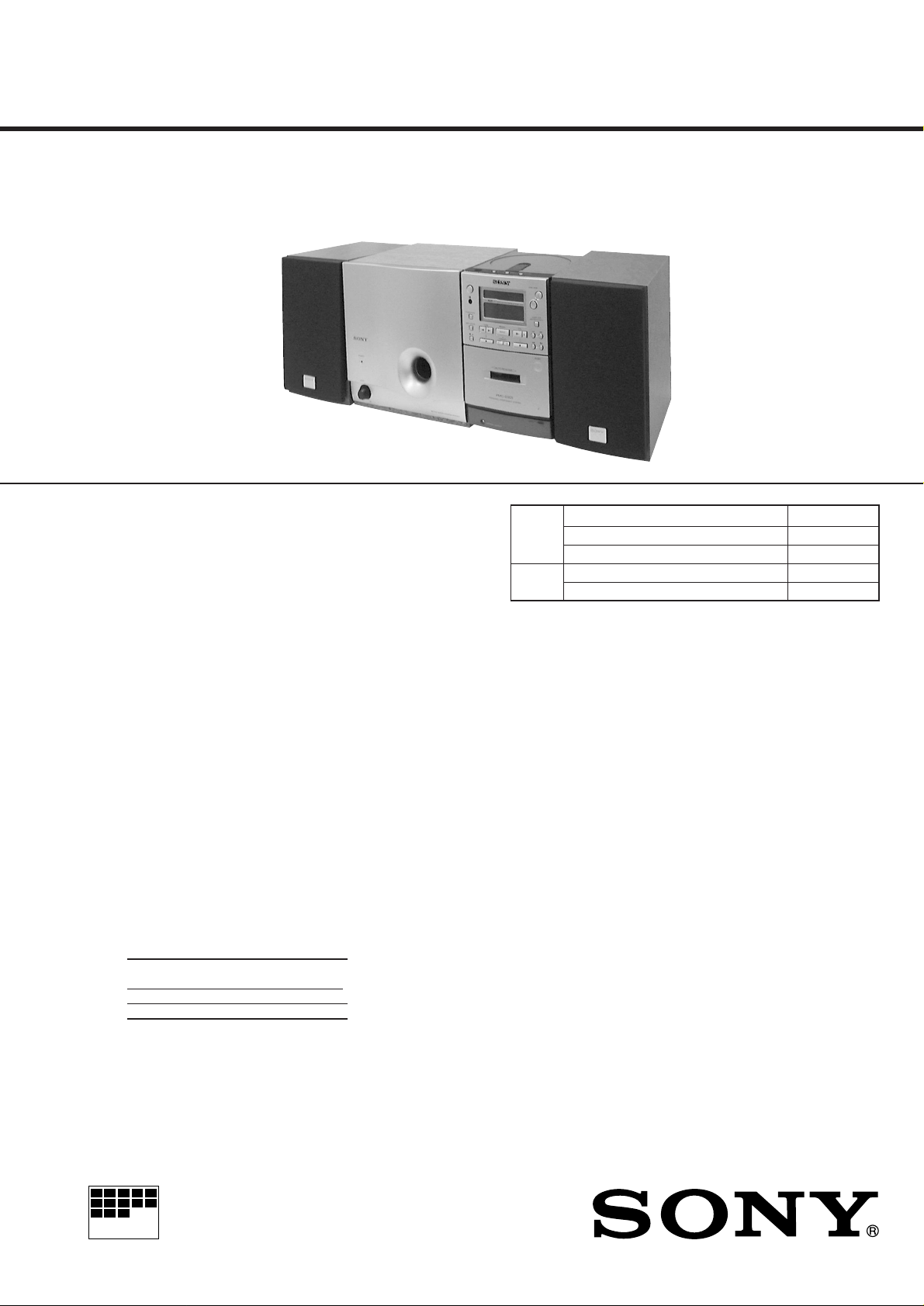
PMC-D407L
SERVICE MANUAL
Ver 1.0 1998. 09
CD
Section
Tape
Section
AEP Model
Model Name Using Similar Mechanism PMC-D307L
CD Mechanism Type KSM-213CDM
Optical Pick-up Name KSS-213C
Model Name Using Similar Mechanism PMC-D307L
T ape Transport Mechanism Type MF-D307
CD player section
System
Compact disc digital audio system
Laser diode properties
Material: GaAlAs
Wave length: 780 nm
Emission duration: Continuous
Laser output: Less than 44.6 µW
(This output is the value measured at a distance of
about 200 mm from the objective lens surface on
the optical pick-up block with 7 mm aperture.)
Spindle speed
200 r/min (rpm) to 500 r/min (rpm) (CLV)
Number of channels
2
Frequency response
20 - 20,000 Hz +1/–2.5 dB
Wow and flutter
Below measurable limit
Radio section
Frequency range
FM Except Italian model 87.6 - 107 MHz
Italian model 87.5 - 108 MHz
MW 531 - 1,602 kHz
LW 153 - 279 kHz
IF
FM: 10.7 MHz
MW/LW: 450 kHz
Aerials
FM: External aerial terminal
MW/LW: External aerial terminal
SPECIFICA TIONS
Cassette-corder section
Recording system
4-track 2-channel stereo
Fast winding time
Approx. 130 s (sec.) with Sony cassette C-60
Frequency response
TYPE I (normal): 40 - 15,000 Hz
Super woofer
Speaker
Woofer: 10 cm (4 in.) dia., 4.0 ohms, cone type
Power output
30 W (at 100 Hz)
Power consumption
AC 30 W
Dimensions (incl. projecting parts)
Approx. 210 × 210 × 247 mm (w/h/d)
(8 3/8 × 8 3/8 × 9 3/4 inches)
Mass
Approx. 4.1 kg (9 lb. 1 oz.)
– Continued on next page –
MICROFILM
PERSONAL COMPONENT SYSTEM
– 1 –
Page 2

General
Speaker
Full range: 8 cm (3 1/4 in.) dia., 6.0 ohms,
cone type × 2
Input
LINE IN jack (stereo minijack)
Minimum input level 250 mV
Outputs
Headphones jack (stereo minijack)
For 16 - 68 ohms impedance headphones
LINE OUT jack (stereo minijack)
Rated output level 440 mV at load impedance
47 kilohms
Optical digital output (optical output connector)
Wave length: 630 - 690 nm
Maximum power output
10 W + 10 W
Power requirements
For personal component system:
230 V AC, 50 Hz
For remote commander:
3 V DC, 2 R6 (size AA) batteries
Power consumption
AC 35 W
Dimensions (incl. projecting parts)
Player: approx. 130 × 211 × 200 mm (w/h/d)
(5 1/8 × 8 3/8 × 7 7/8 inches)
Left speaker: approx. 130 × 210 × 235 mm
(w/h/d) (5 1/8 × 8 3/8 × 9 3/8 inches)
Right speaker: approx. 130 × 210 × 200 mm
(w/h/d) (5 1/8 × 8 3/8 × 7 7/8 inches)
Mass
Player: approx. 1.7 kg (3 lb. 12 oz.)
Left speaker: approx. 3.2 kg (7 lb. 1 oz.)
Right speaker: approx. 1.6 kg (3 lb. 9 oz.)
Supplied accessories
Remote commander RMT-C305AD (1)
FM lead aerial (1)
MW/LW loop aerial (1)
Audio connecting cord (2)
Design and specifications are subject to change without
notice.
TABLE OF CONTENTS
1. SERVICING NOTES......................................................... 3
2. GENERAL
2-1. Location of Controls ........................................................... 4
3. DISASSEMBLY
3-1. Cabinet (Rear) Section ........................................................ 5
3-2. Case (Lower) Section .......................................................... 6
3-3. Tape Mechanism Deck, Line Board .................................... 6
3-4. Cabinet (CD) Section .......................................................... 7
3-5. CD, System Board...............................................................7
3-6. RDS Board, LCD Section ................................................... 8
3-7. Optical Pick-up Section.......................................................8
3-8. Rear Chassis (Speaker) Assy ............................................... 9
3-9. Power Amp, Terminal, Jack Board...................................... 9
3-10. Power Board...................................................................... 10
3-11. Rear Chassis (Woofer Speaker) Assy................................ 10
3-12. S/Woofer Amp Board........................................................ 11
3-13. Woofer Power Board ......................................................... 11
4. MECHANICAL ADJUSTMENTS............................... 12
5. ELECTRICAL ADJUSTMENTS
Tape Section .......................................................................... 12
Tuner Section......................................................................... 14
CD Section ............................................................................ 16
6. DIAGRAMS
6-1. IC Pin Description............................................................. 20
6-2. Circuit Boards Location .................................................... 21
6-3. Block Diagram –Tuner Section–....................................... 23
6-4. Block Diagram –CD Section–........................................... 25
6-5. Block Diagram –Tape Section– ........................................ 27
6-6. Printed Wiring Board –Tuner Section– ............................. 29
6-7. Schematic Diagram –Tuner Section–................................ 31
6-8. Printed Wiring Boards –RDS Section– ............................. 33
6-9. Schematic Diagram –RDS Section– ................................. 35
6-10. Printed Wiring Boards –CD Section– ............................... 37
6-11. Schematic Diagram –CD Section–.................................... 39
6-12. Printed Wiring Boards –Main Section– ............................ 42
6-13. Schematic Diagram –Main Section–................................. 45
6-14. Printed Wiring Boards –Control Section–......................... 48
6-15. Schematic Diagram –Control Section– ............................. 51
6-16. Printed Wiring Boards –Woofer Speaker Section– ........... 55
6-17. Schematic Diagram –Woofer Speaker Section– ............... 57
6-18. Printed Wiring Boards –Power Amplifier Section– .......... 59
6-19. Schematic Diagram –Power Amplifier Section– .............. 61
SAFETY-RELATED COMPONENT WARNING!!
COMPONENTS IDENTIFIED BY MARK ! OR DOTTED LINE
WITH MARK ! ON THE SCHEMATIC DIAGRAMS AND IN
THE PARTS LIST ARE CRITICAL TO SAFE OPERATION.
REPLACE THESE COMPONENTS WITH SONY PAR TS WHOSE
P AR T NUMBERS APPEAR AS SHO WN IN THIS MANUAL OR
IN SUPPLEMENTS PUBLISHED BY SONY.
7. EXPLODED VIEWS
7-1. Case Section ...................................................................... 68
7-2. Cabinet (Front) Section ..................................................... 69
7-3. Cabinet (CD) Section ........................................................ 70
7-4. Optical Pick-up Section..................................................... 71
7-5. Tape Mechanism Deck Section-1 ...................................... 72
7-6. Tape Mechanism Deck Section-2 ...................................... 73
7-7. Speaker (L) Section........................................................... 74
7-8. Speaker (R) Section........................................................... 75
7-9. Woofer Speaker Section .................................................... 76
8. ELECTRICAL PARTS LIST ........................................ 77
– 2 –
Page 3
SECTION 1
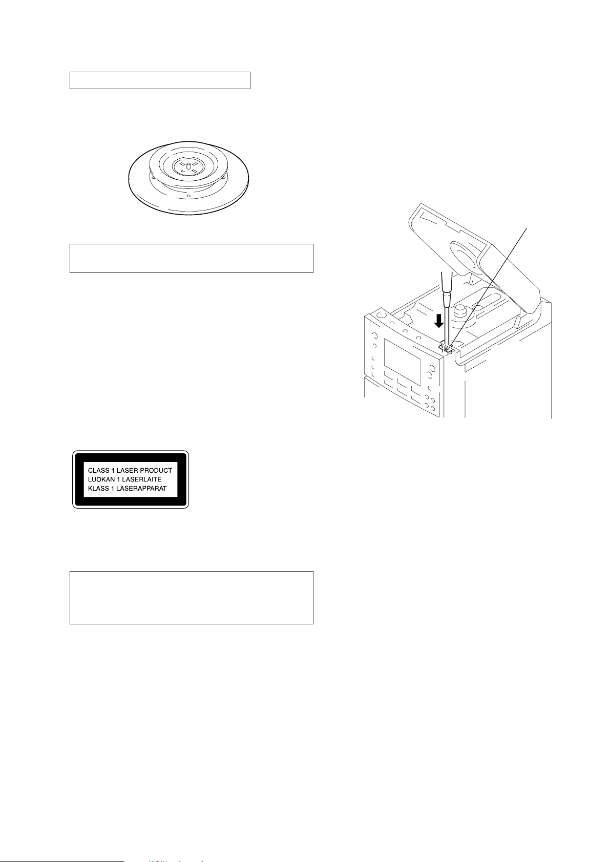
SERVICING NOTES
CHUCK PLATE JIG ON REPAIRING
On repairing CD section, playing a disc without the lid (CD), use
Chuck Plate Jig.
• Code number of Chuck Plate Jig: X-4918-255-1
NOTES ON HANDLING THE OPTICAL PICK-UP
BLOCK OR BASE UNIT
The laser diode in the optical pick-up block may suffer electrostatic
breakdown because of the potential difference generated by the
charged electrostatic load, etc. on clothing and the human body.
During repair, pay attention to electrostatic breakdown and also use
the procedure in the printed matter which is included in the repair
parts.
The flexible board is easily damaged and should be handled with
care.
LASER DIODE AND FOCUS SEARCH OPERATION
CHECK
1. Turn OPERATE switch on with to disc inserted and press
FUNCTION button to CD position.
2. Open the lid (CD).
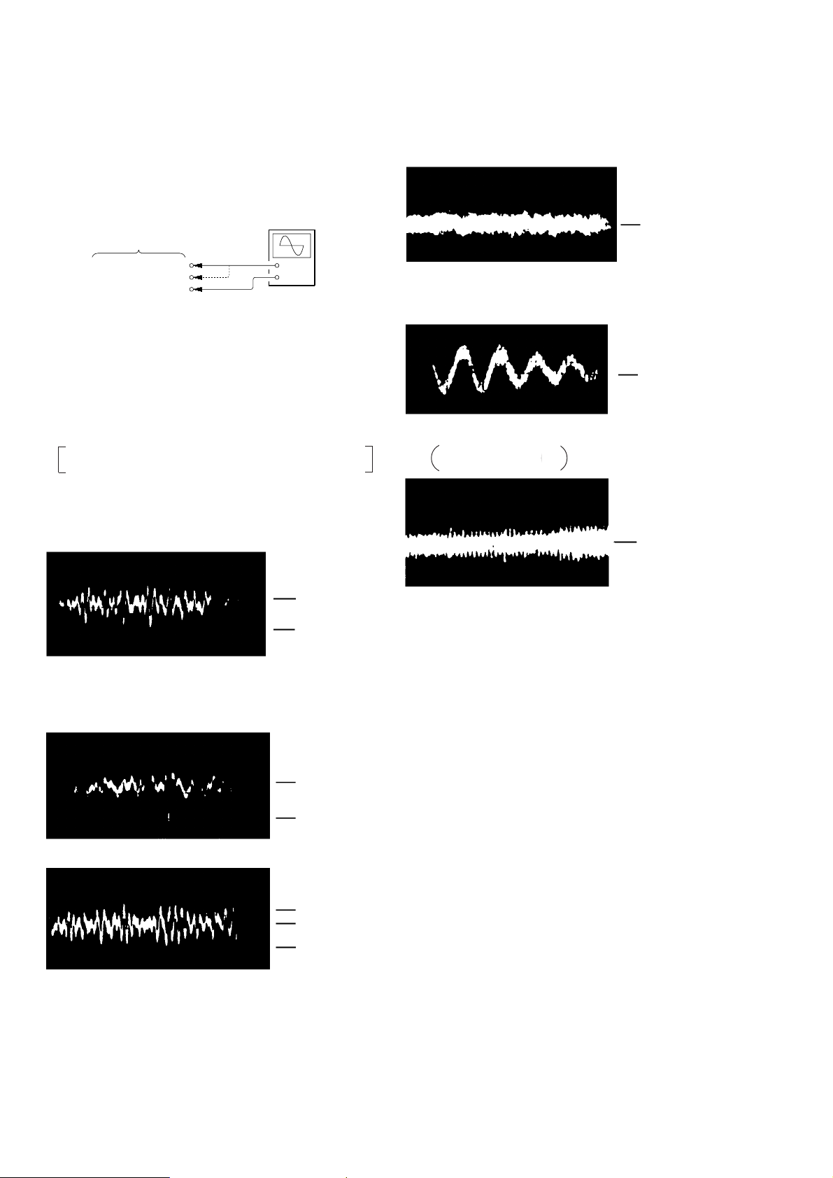
3. Turn on S801 as following figure.
4. Press the ( (CD) button.
5. Confirm the laser diode emission while observing the objecting
lens. When there is no emission, Auto Po wer Control circuit or
Optical Pick-up is broken.
Objective lens moves up and do wn three times for focus search.
S801
NOTES ON LASER DIODE EMISSION CHECK
The laser beam on this model is concentrated so as to be focused on
the disc reflective surface by the objective lens in the optical pickup block. Therefore, when checking the laser diode emission, observe from more than 30 cm away from the objective lens.
This Compact Disc player is classified as a
CLASS 1 LASER product.
The CLASS 1 LASER PRODUCT table is
location on the rear exterior.
CAUTION
Use of controls or adjustments or performance of procedures
other than those specified herein may result in hazardous radiation exposure.
– 3 –
Page 4
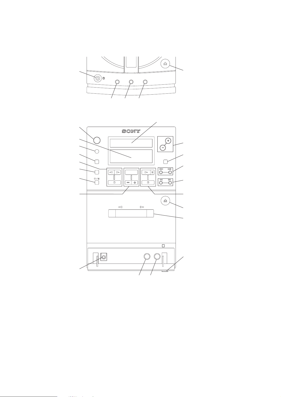
2-1. LOCATION OF CONTROLS
SECTION 2
GENERAL
– upper side view –
5
7
8
9
10
11
12
13
14
– front side view –
1
234
6
16
17
18
19
20
15
1. 6 PUSH OPEN/CLOSE button (CD)
2. PLAY MODE MONO/ST ISS button
3. PGM SET AUTO PRESET button
4. SOUND button
5. 2 (Headphones) jack
6. RDS display window
7. OPERATE (power) button
8. Display window
9. Remote sensor window
10. FUNCTION button
11. TAPE operation buttons
9 (Reverse side playback) button
( (Front side playback) button
p (Stop) button
12. DIR MODE button
13. r/P (Recording/pause) button
21
22
23
2425
14. RADIO operation buttons
BAND button
PRESET – button
PRESET + button
15. OPTICAL DIGITAL OUT (CD) jack
16. VOLUME +/– button
17. DISPLAY ENTER/MEM button
18. =/+, TUNE –/+ button
19. 0/) button
20. CD operation buttons
( (Playback) button
P (Pause) button
p (Stop) button
21. 6 PUSH (cassette holder open) button
22. Cassette holder
23. OPEN $ knob
24. LINE OUT jack
25. LINE IN jack
– 4 –
Page 5
SECTION 3
DISASSEMBLY
• The equipment can be removed using the following procedure.
Set Cabinet (rear) Case (lower) Cabinet (CD) CD, System RDS board, LCD section
section section section board Optical pick-up section
Tape mechanism deck, Line board
Rear chassis (speaker) assy Power Amp, Terminal, Jack board Power board
Rear chassis (woofer speaker) assy S/Woofer Amp board Woofer power board
Note : Follow the disassembly procedure in the numerical order given.
3-1. CABINET (REAR) SECTION
2
KTP 3x10
1
KTP 3x10
6
cabinet (rear) section
4
BVTP 3x10
5
KH312
3
BVTP 3x10
– 5 –
Page 6
3-2. CASE (LOWER) SECTION
4
BVTP 3x10
3
earth lead
5
case (lower) section
1
parallel wire (27 core)
(CNP801)
2
CNP3, 301, 303, 305, 307, 310, 311
3-3. TAPE MECHANISM DECK, LINE BOARD
3
BVTP 3x10
5
BVTP 3x10
7
LINE board
2
P 2.6x8
4
BVTP 3x10
6
tape mechanism
deck
1
CNP705
– 6 –
Page 7
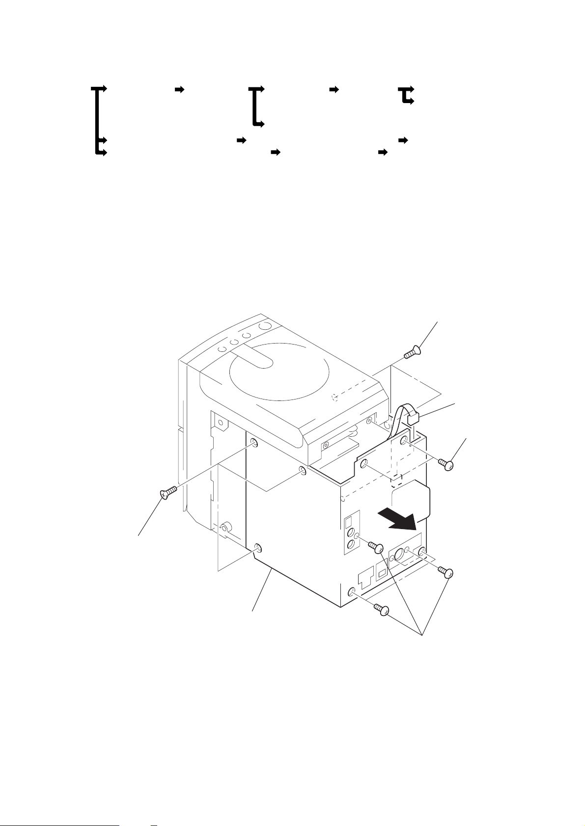
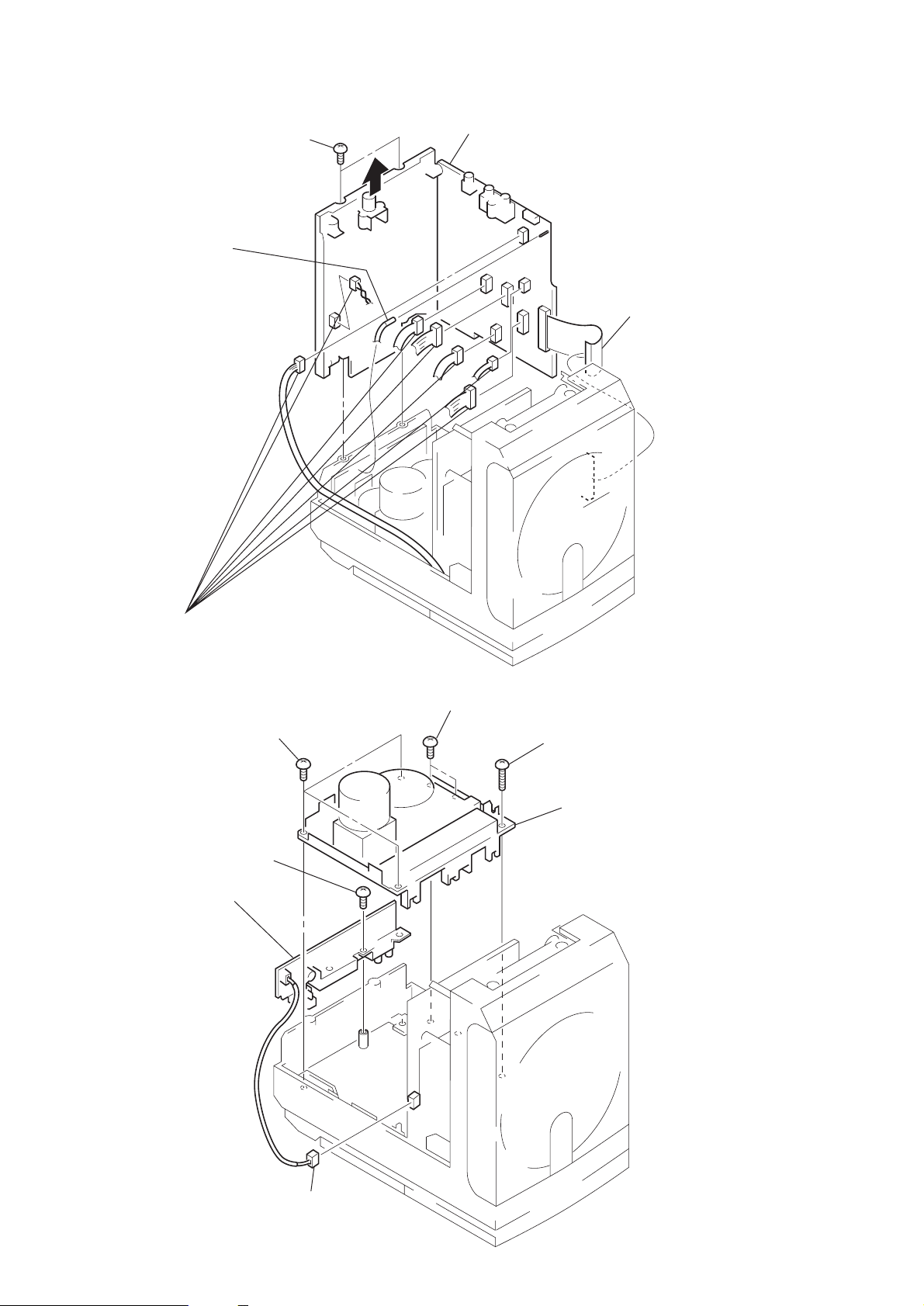
3-4. CABINET (CD) SECTION
1
CNP705
4
cabinet (CD) section
3
CNP802, 803
3-5. CD, SYSTEM BOARD
9
BVTP 3x10
2
FFC cable 16P
(optical pick-up)
5
CD board
2
claws
4
BVTP 3x10
3
parallel wire (9 core)
(CNP706)
0
SYSTEM board
8
BTP 2.6x8
7
CNP804
1
CNP707
– 7 –
6
S801
Page 8
3-6. RDS BOARD, LCD SECTION
4
P 2.6x8
3
P 2.6x8
5
RDS board
1
2
parallel wire (19 core)
(CNP402, 403)
parallel wire (19 core)
(CNP401, 404)
7
LCD section
3-7. OPTICAL PICK-UP SECTION
1
screw (2.6x16)
6
BTP 2.6x8
2
optical pick-up section
– 8 –
Page 9
g
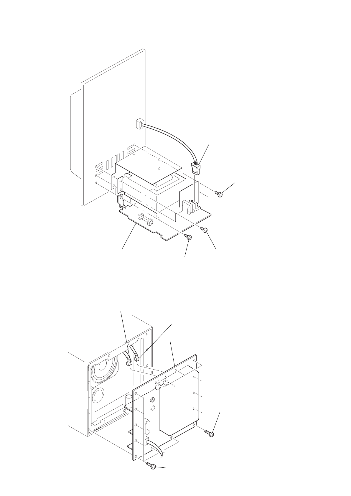
3-8. REAR CHASSIS (SPEAKER) ASSY
0
3
CNP504
4
rear chassis (speaker) assy
1
screw B tappin
3-9. POWER AMP, TERMINAL, JACK BOARD
6
BTP 3x10
5
BVTP 3x10
2
screw B tapping
9
JACK board
8
TERMINAL board
1
CNP503
3
BVTP 3x1
2
CNP505
7
POWER AMP board
4
BVTP 3x10
– 9 –
Page 10
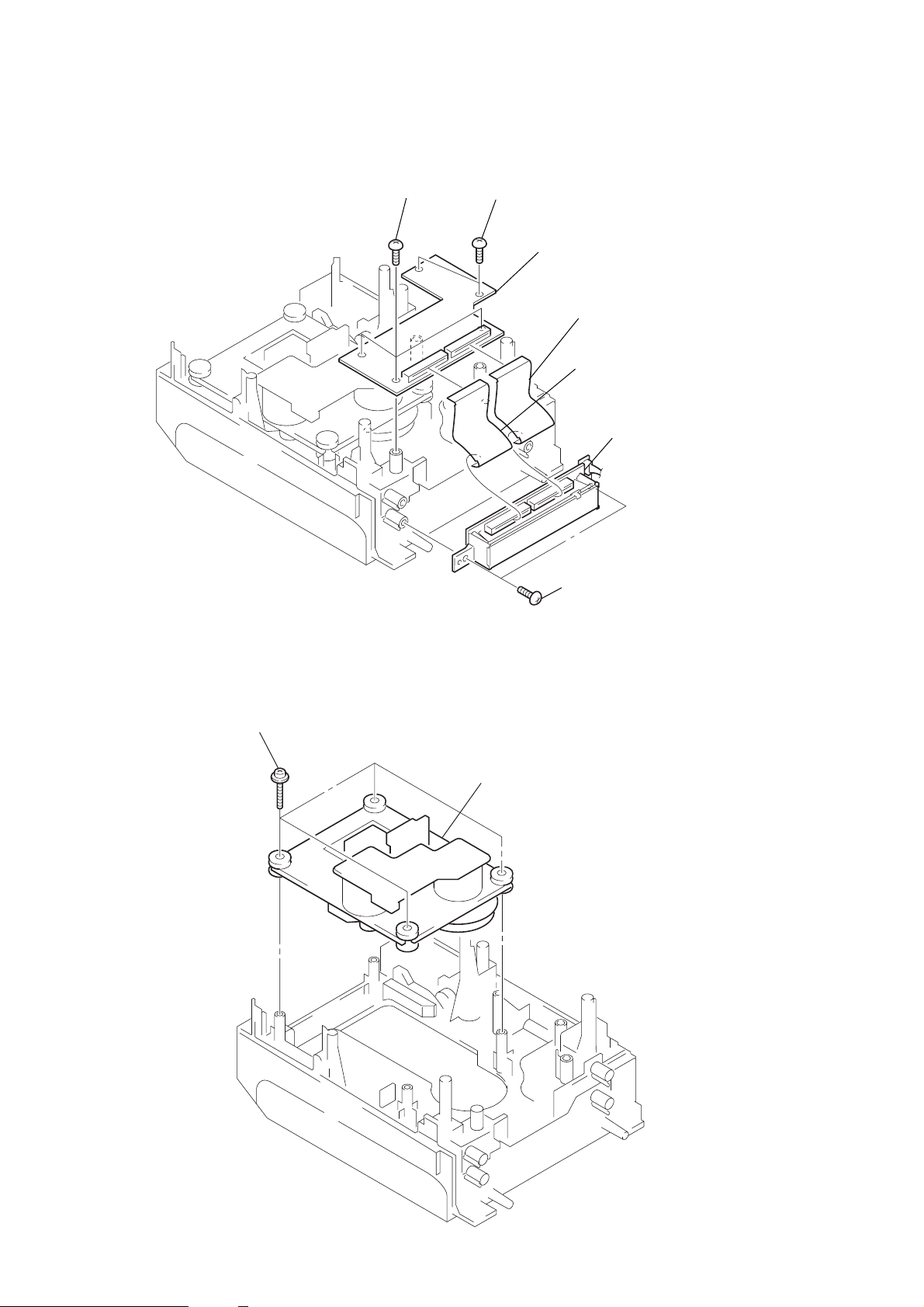
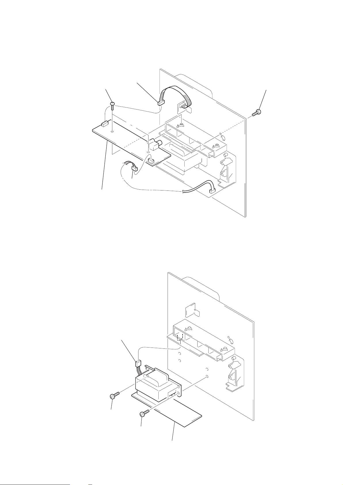
3-10. POWER BOARD
6
1
CNP501
4
P 4x
5
POWER board
3-11. REAR CHASSIS (WOOFER SPEAKER) ASSY
4
CNP601
3
P 4x6
2
P 3x6
3
CNP603
5
rear chassis (woofer speaker) assy
1
screw +B tapping
2
– 10 –
screw +B tapping
Page 11
3-12. S/WOOFER AMP BOARD
0
3
BVTP 3x10
5
S/WOOFER AMP board
1
2
CNP602
CNP605
4
BTP 3x1
3-13. WOOFER POWER BOARD
1
2
P 4x6
CNP606
3
P 4x6
4
WOOFER POWER board
– 11 –
Page 12
SECTION 4
MECHANICAL ADJUSTMENTS
SECTION 5
ELECTRICAL ADJUSTMENTS
PRECAUTION
1. Clean the following parts with a denatured-alcohol-moistened
swab:
record/playback/erase head pinch roller
rubber belts capstan
idlers
2. Demagnetize the record/playback/erase head with a head demagnetizer. (Do not bring the head demagnetizer close to the
erase head.)
3. Do not use a magnetized screwdriver for the adjustments.
4. After the adjustments, apply suitable locking compound to the
parts adjusted.
5. The adjustments should be performed with the rated power supply voltage unless otherwise noted.
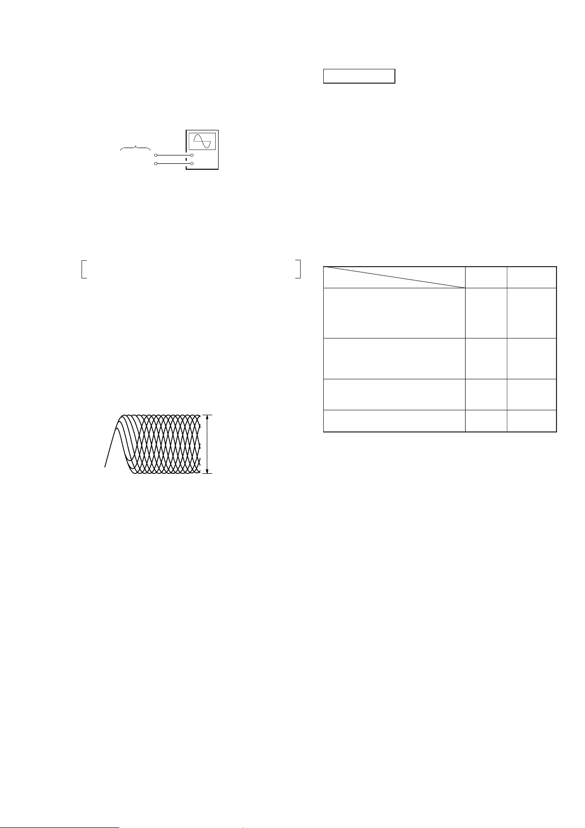
Torque Measurement
Mode Torque Meter Meter Reading
FWD
FWD 2.0 – 6.0 g•cm
Back tension (0.028 – 0.076 oz•inch)
REV
REV 2.0 – 6.0 g•cm
Back tension (0.028 – 0.076 oz•inch)
FF, REW CQ-201B
CQ-102C
CQ-102RC
30 – 70 g•cm
(0.42 – 1.02 oz•inch)
30 – 70 g•cm
(0.42 – 1.02 oz•inch)
80 – 170 g•cm
(1.12 – 2.38 oz•inch)
T ape Tension Measurement
Mode Tension Meter Meter Reading
FWD CQ-403A
REV CQ-403R
more than 90 g
(more than 3.17 oz)
TAPE SECTION 0 dB = 0.775 V
1. The adjustments should be performed in the order given in the
service manual. (As a general rule. Playback circuit adjustment
should be completed before performing recording circuit adjustment.)
2. The adjustments should be performed for both L-ch and R-ch
unless otherwise indicated.
Standard Output Level
SP OUT PHONES
Load impedance 6 Ω 32 Ω
Output level 0.775 V (0 dB) 0.25 V (–10 dB)
Test T ape
Type Signal Used for
WS-48B 3 kHz, 0 dB Tape speed adjustment
P-4-A063 6.3 kHz, –10 dB Head azimuth adjustment
Tape Speed Adjustment
Procedure:
Mode: playback
digital frequency
test tape
WS-48B
(3 kHz, 0 dB)
set
2
Adjust so that the value on the frequency counter is 3 kHz.
counter
32
Ω
(headphones) jack
Specification Values:
Digital frequency counter
2,970 to 3,030 Hz
Adjust so that the frequency at the beginning and that at the end of
tape winding are between 2,970 and 3,030 Hz.
Adjustment Location:
adjustable
resistor
M691
– 12 –
Page 13
Record/Playback Head Azimuth Adjustment
k
Procedure:
1. Mode: playback
test tape
P-4-A063
(6.3 kHz, –10 dB)
set
2
level meter
Ω
32
+
–
(headphones) jac
2. Turn the adjustment screw for the maximum output levels. If
these levels do not match, turn the adjustment screw
until both
of output levels match together within 1 dB.
Adjustment Location:
forward
L-CH
peak
screw
position
3. Phase Check
Mode: playback
test tape
P-4-A063
(6.3 kHz, –10 dB)
R-CH
peak
L-CH
set
R-CH
within
1dB
output
level
32
32
2
(headphones) jack
Screen pattern
L-CH
peak
Ω
Ω
R-CH
peak
oscilloscope
H
V
+
+
–
–
within
1dB
screw
angle
reverse
screwdriver
in phase 45
Good Wrong
90 °135 °180
°
°
4. After the adjustment, lock the screws with locking compound.
– 13 –
Page 14
TUNER SECTION 0 dB = 1 µV
)
Precautions in Repairing
Note : As a tuner unit (TU1) is difficult to repair if faulty,
replace it with new one.
• FM Section
Setting:
FUNCTION button: FM
FM RF signal
generator
0.01
22.5 kHz frequency
deviation by 400 Hz signal
output level : as low as possible
• MW/LW Section
Setting:
FUNCTION button: MW or LW
AM RF signal
generator
EXT ANT FM
jack (CNP2)
µ
F
set
Put the lead-wire
antenna close to
the set.
FM FREQUENCY COVERAGE
ADJUSTMENT
Frequency Display 87.5 MHz 108 MHz
Reading on Digital voltmeter 1.3 V or more 9.0 V or less
Adjustment Part <confirmation> <confirmation>
FM TRACKING ADJUSTMENT
Adjust for a maximum reading on level meter.
<confirmation> <confirmation>
87.5 MHz 108 MHz
MW FREQUENCY COVERAGE
ADJUSTMENT
Frequency Display 531 kHz 1,611 kHz
Reading on Digital voltmeter 0.85 ± 0.5 V 6.8 ± 1.5 V
Adjustment Part <confirmation> <confirmation>
MW TRACKING ADJUSTMENT
Adjust for a maximum reading on level meter.
L3 CT4
621 kHz 1,404 kHz
30% amplitude
modulation by 400 Hz signal
output level : as low as possible
• Connecting Level Meter (FM, MW and LW)
level meter
(range: 0.5-5 V ac
Ω
32
set
2
(headphones) jack
• Connecting Digital Voltmeter (FM, MW and LW)
digital
voltmeter
tuner board
TP (VT)
AM IF ADJUSTMENT
Adjust for a maximum reading on level meter.
CFT1
450 kHz
LW FREQUENCY COVERAGE
ADJUSTMENT
Frequency Display 153 kHz 279 kHz
Reading on Digital voltmeter 0.6 ± 0.4 V 7.5 ± 0.5 V
Adjustment Part <confirmation> L4
L W TRACKING ADJUSTMENT
Adjust for a maximum reading on level meter.
L5 CT5
162 kHz 261 kHz
Adjustment Location: TUNER board (See page 15.)
• Repeat the procedures in each adjustment se veral times, and the
frequency coverage and tracking adjustments should be finally
done by the trimmer capacitors.
– 14 –
Page 15
Adjustment Location:
T
– tuner board (component side) –
TP
(VT)
CFT1
AM IF
ADJUSTMENT
IC1
L4
LW
FREQUENCY
COVERAGE
ADJUSTMENT
TU1
CT4 L3
MW
TRACKING
ADJUSTMENT
CT5
L5
LW
TRACKING
ADJUSTMEN
– 15 –
Page 16
CD SECTION
Notes on Adjustment
1. Perform adjustment in test mode.
After adjustments, be sure to release test mode.
2. Perform adjustments in the order given.
3. Use the disc (YEDS-18. Part No. 3-702-101-01) only when so
indicated.
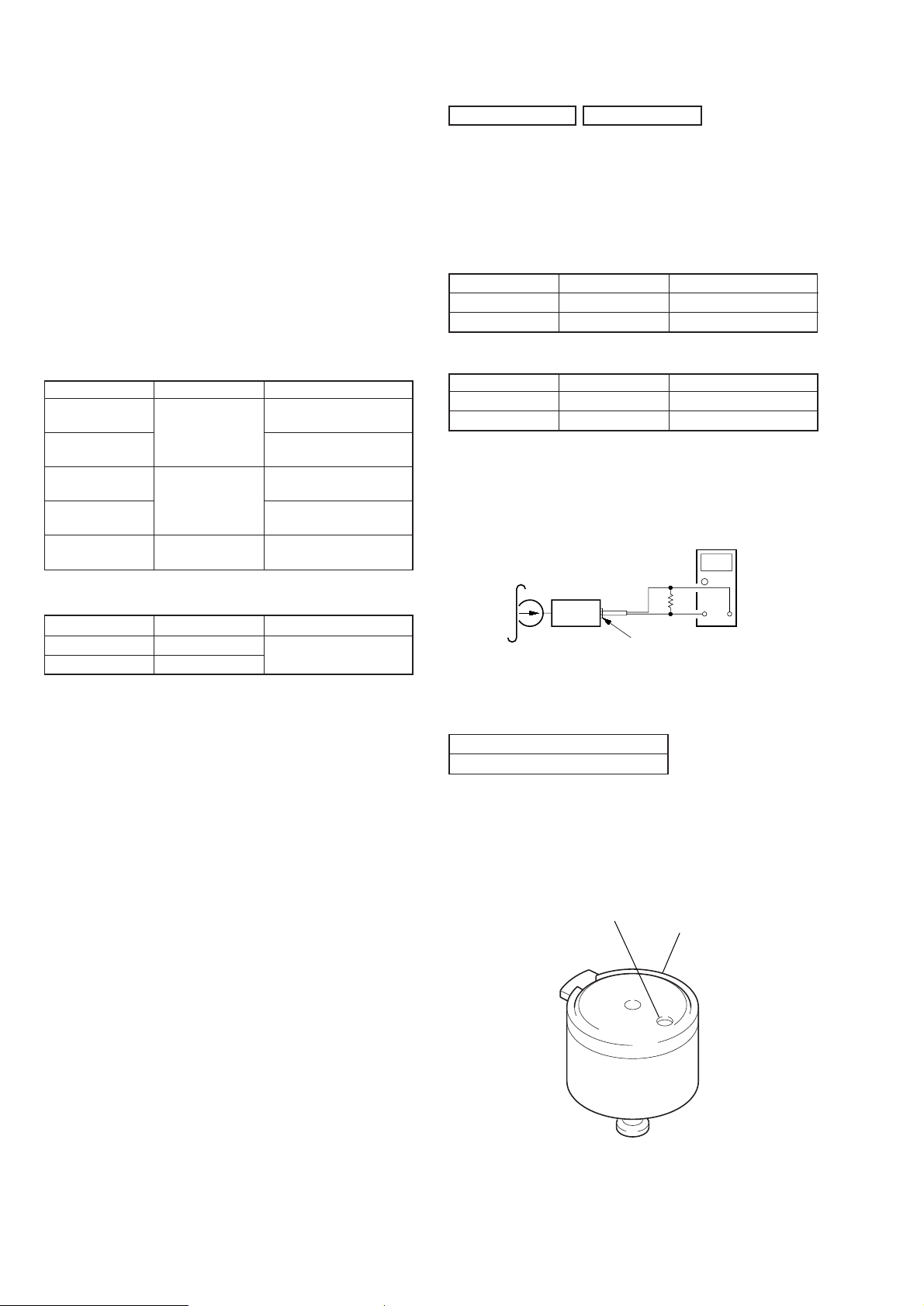
How to Put the Set into Test Mode
1. Disconnect an AC plug cord. (Power is not applied to the set.)
2. Solder across the TEST1 terminal.
3. Close the lid (CD).
4. Connect an AC plug cord.
[SW1 BOARD] (Conductor Side)
TEST1
terminal
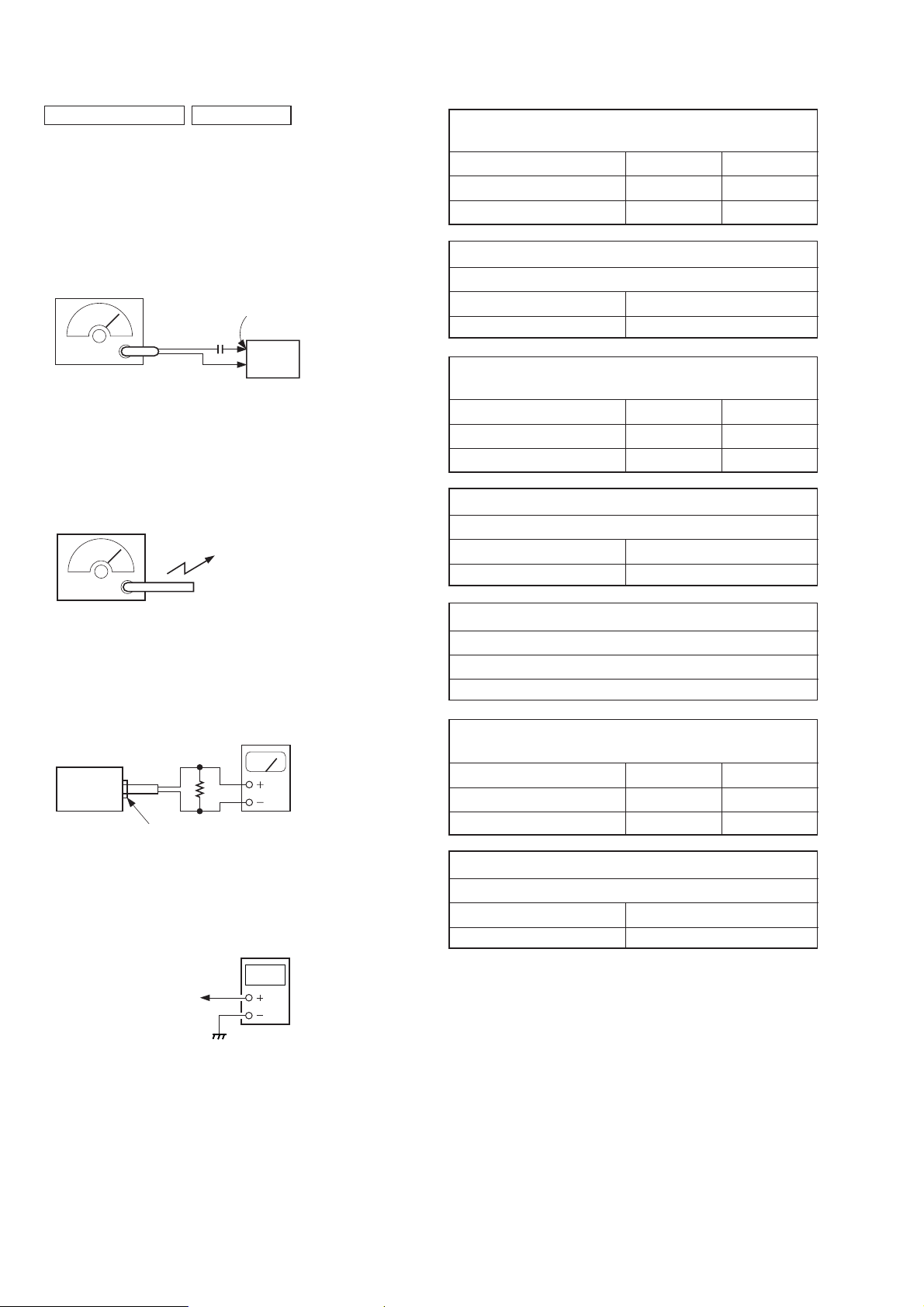
E-F Balance Adjustment
This adjustment is to be done when the optical pick-up is replaced.
Procedure:
oscilloscope
(DC range)
CD board
TP (TRACKING-Y)
TP (VC)
+
–
1. Connect the oscilloscope to TP (TRACKING-Y) and TP (VC)
on the CD board.
2. Insert the disc (YEDS-18) in and close the lid (CD).
3. Put the set into test mode.
4. Press the + and = buttons to move the optical pick-up to
the center.
5. Press the ( button.
From focus searching, focus is turned ON while entering
CLV drawing-in mode. Tracking and sled are turned OFF.
6. Adjust R V703 so tha t the oscilloscope traverse wav eform is symmetrical, as shown in the figure below.
Note: Take long sweep time
VOLT/DIV: 0.2 V (with the 10:1 probe in use.)
TIME/DIV: 1 ms
for easy monitoring.
How to Release the Test Mode
1. Be sure to disconnect the AC plug cord and remove the solder
bridge at the TEST1 terminal connected before in setting.
2. The set thus becomes available for normal operation
Before Beginning Adjustment
Put the set into test mode and perform the following checks.
Repair if there are any problems.
• Sled Motor Check
Press the +, = buttons and confirm that the optical pick-up
moves smoothly from the innermost to outermost circumference
and back smoothly and with no catching or abnormal noises.
+ : Optical pick-up moves to the outer circumference
= : Optical pick-up moves to the inner circumference
• Focus Search Check
1. Press the ( button. (Focus search operation is performed continuously.)
2. Look at the optical pick-up objective lens and confirm that it
moves up and down smoothly, when no catching or abnormal
noises.
3. Press the p button.
Confirm that focus search operation stops. If it does not , press
the p button again longer.
A
0 V
A=B
B
0 V
Adjustment value: 0.4 ± 0.2 Vp-p (A + B)
7. Release the test mode after adjustment is completed.
Adjustment Location: CD board (See page 19.)
A
B
A=B
Note: When the malfunction is occurred by mis-passing other keys, turn
off the power and check again from making the test mode.
– 16 –
Page 17
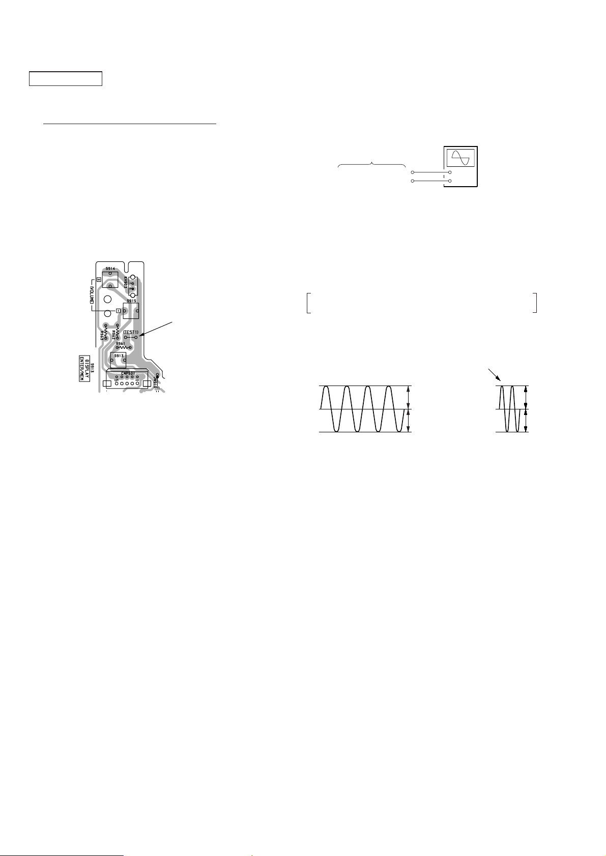
Focus Bias Adjustment
This adjustment is to be done when the optical pick-up is replaced.
Procedure:
oscilloscope
(AC range)
CD board
TP (RF)
TP (VC)
+
–
1. Connect the oscilloscope TP (RF) and TP (VC) on the CD board.
2. Insert the disc (YEDS-18) in and close the lid for CD.
3. Put the set into test mode. (See page 16.)
4. Press + and = buttons to move the optical pick-up to the
center. (Move the optical pick-up to the music area on the disc
to enable easy visibility of the eye pattern.)
5. Press the ( button.
From focus searching, focus is turned ON while entering
CLV drawing-in mode. Tracking and sled are turned OFF.
6. Press the ( button.
[Both tracking and sled are turned ON.]
7. Adjust RV701 so that the oscilloscope waveform is as sho wn in
the figure below. (eye pattern)
A good eye pattern means that the diamond shape (≈ ) in the
center of the waveform can be clearly distinguished.
• RF signal reference waveform (eye pattern)
VOLT/DIV : 0.2 V (With the 10:1 probe in use)
TIME/DIV : 500 ns
1.3
±
0.2 Vp-p
REFERENCE
Focus/Tracking Gain Adjustment
A frequency response analyzer is necessary in order to perform this
adjustment exactly .
However , this gain has a mar gin, so e ven if it is slightly off, there is
no problem. Therefore, do not perform this adjustment.
Focus/tracking gain determines the pick-up follow-up (vertical and
horizontal) relative to mechanical noise and mechanical shock when
the 2-axis device operate.
However, as these reciprocate, the adjustment is at the point where
both are satisfied.
• When gain is raised, the noise when the 2-axis device operates
increases.
• When gain is lowered, mechanical shock and skipping occurs
more easily.
• When gain adjustment is off, the symptoms below appear.
Gain
Symptoms
• The time until music starts becomes
longer for p→( on automatic
selection. low low or high
(=, + buttons pressed.)
(Normally takes about 2 seconds.)
• Music does not start and disc
continues to rotate for p→( or
automatic selection.
(=, + buttons pressed.)
• Sound is interrupted during PLAY.
Or time counter display stops — low
progressing.
• More noise during 2-axis device
operation.
Focus Tracking
—low
high high
When observing the eye pattern, set the oscilloscope for AC
range and raise vertical sensitivity.
8. Release the test mode after adjustment is completed.
Adjustment Location: CD board (See page 19.)
– 17 –
Page 18
The following is a simple adjustment method.
– Simple Adjustment –
Note:Since exact adjustment cannot be performed, remember the posi-
tions of the controls before performing the adjustment. If the positions after the primary adjustment are only a little different, return
the controls to the original position.
oscillosope
(DC range)
CD board
8. Connect the oscilloscope to TP (TRACKING-Y) and TP (VC)
on the CD board.
9. Adjust RV704 so that the waveform is as shown in the figure
below. (tracking gain adjustment)
VOLT/DIV: 1 V
TIME/DIV:2 ms
0 V
TP (FOCUS-Y)
TP (TRACKING-Y)
TP (VC)
+
–
Procedure:
1. Keep the set horizontal.
If the set is not horizontal, this adjustment cannot be performed
due to the gravity against the 2-axis device.
2. Connect the oscilloscope TP (FOCUS-Y) and TP (VC) on the
CD board.
3. Insert the disc (YEDS-18) in and close the lid for CD.
4. Put the set into test mode. (See page 16.)
5. Press the ( button.
From focus searching, focus is turned ON while entering
CLV drawing-in mode. Tracking and sled are turned OFF.
6. Press the ( button.
[Both tracking and sled are turned ON.]
7. Adjust RV702 so that the waveform is as shown in the figure
below. (Focus gain adjustment)
VOLT/DIV: 100 mV
TIME/DIV:2ms
100 mV
0 V
• Inconnect Examples (DC level changes more than on adjusted
waveform)
• Incorrect Examples (fundamental wave appears)
low tracking gain
VOLT/DIV: 1 V
TIME/DIV: 2ms
0 V
high tracking gain
high fundamental wave
than for low gain
VOLT/DIV: 1 V
TIME/DIV: 2ms
0 V
Note:
VOLT/DIV: with the 10:1 probe in used.
10. Release test mode after adjustment is completed.
Adjustment Location: CD board (See page 19.)
low focus gain
high focus gain
VOLT/DIV: 100 mV
TIME/DIV:2ms
250 mV
0 V
VOLT/DIV: 100 mV
TIME/DIV:2ms
100 mV
75 mV
0 V
– 18 –
Page 19
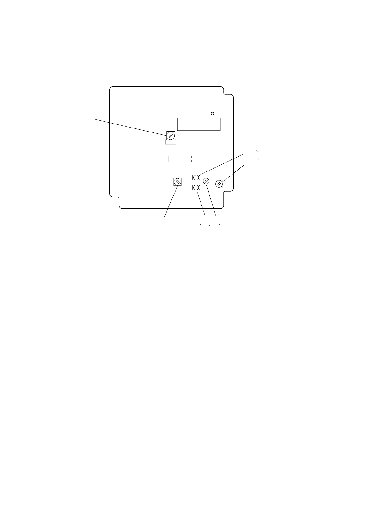
Connection and Adjustment Location:
)
–CD board (conductor side)–
TP
(RF)
RF
TRACKING
TP
(FOCUS-Y
IC701
X
VC
Y
Y
FOCUS
X
–CD board (component side)–
FOCUS BIAS
ADJUSTMENT
CNP706
RV701
TP
(TRACKING-Y)
RV703
E-F BALANCE
ADJUSTMENT
TP
(VC)
RV704
TRACKING GAIN
ADJUSTMENT
RV702
FOCUS GAIN
ADJUSTMENT
CNP701
– 19 –
Page 20

SECTION 6
DIAGRAMS
6-1. IC PIN DESCRIPTION
• IC801 CXP83120A-022Q (SYSTEM CONTROL, LCD DRIVE)
Pin No. Pin Name I/O Pin Description
1 AC CHK I AC check input
2 C-SCOR I CD-SCOR input
3 RMC I Remote commander input
4 C-XRST O CD system reset output
5 C-XLAT O CD DSP (IC702) command latch output
6 C-DAT O CD DSP (IC702) command data output
7 C-CLK O Clock output for CD DSP (IC702) command
8 C-DOOR I Open/close detection input (“L”: close, “H”: open)
9 328/332 I 328/332 select input (Fixed at “H”.)
10 C-SENS I CD-SENS input
11 C-SQCK O Clock output for CD SUB-Q.
12 C-SQSO I CD SUB-Q input
13 T-BIAS I Tape REC BIAS input
14 — — Not used. (Open)
15 T-REC I Tape REC input
16 T-SOL O Plunger control output
17 T-MODE O HEAD switching output
18 T-AMS I AMS sensitivity switching
19 T-MCON O Motor control output (“H”: Motor ON)
20 P-CON O Power on/off control output
21 V-CLK O Volume clock output
22 V-DAT O Volume data output
23 V-CE O Electrical volume (IC302) chip enable output
24 R-ST I Stereo detection input
25 R-COUNT I Tuner PLL IC count input
26 R-DAT O Tuner PLL IC data output
27 R-CLK O Tuner PLL IC clock output
28 R-CE O Tuner PLL IC chip enable output
29 9K/10K I 9K/10K select input (Fixed at “H”.)
30 T-STAT I Tape detection input
31 – 34 KEY-0 – 3 I Key return signal input
35 INIT O Initial setting output (Not used.)
36 SIMUKE I Destination setting terminal (Fixed at “H”.)
37 SFC O Shift clock ON/OFF out
38 RST I Reset input
39 EXTAL1 I Clock oscillation input (4.19 MHz)
40 XTAL1 O Clock oscillation output (4.19 MHz)
41 VSS — Ground (for A/D converter)
42 XTAL2 O Clock oscillation output (Not used.)
43 EXTAL2 I Clock oscillation output (Fixed at “L”.)
44 AVREF I Reference voltage input (for A/D converter)
45 AVSS — Ground (for A/D converter)
46 VL O LCD bias resistor current control terminal (Cut off at standby)
47 – 49 VLC3 – 1 — LCD bias power supply terminal
50 – 53 COM0 – 3 O LCD common signal output terminal
54 – 77 SEG0 – 23 O LCD segment signal output terminal
78 – 84 NC — Not used. (Open)
85 – 87 — — Not used. (Open)
88 BL-CONT O LCD Back light control output
89 VDD — Power supply (+5 V)
– 20 –
Page 21
Pin No. Pin Name I/O Pin Description
90 NC — Connected to the power supply.
91 VSS — Ground
92 TX O Crystal connection for clock oscillation. (32.768 kHz)
93 TEX I Crystal connection for clock oscillation. (32.768 kHz)
94 C-MUTE O Mute output for CD.
95 B-MUTE O Mute output for Tuner.
96 A-MUTE O Mute output for Audio.
97 ISS1 I ISS1 switch input
98 ISS2 I ISS2 switch input
99 T-END I Tape end detection input
100 NC — Not used. (Open)
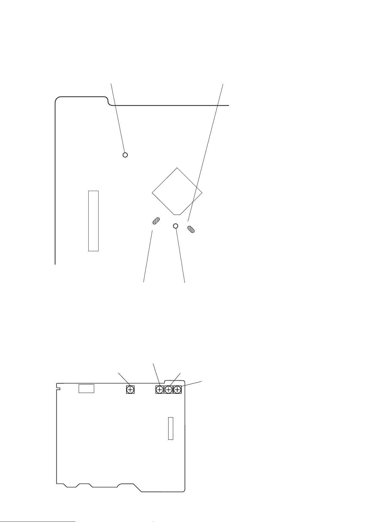
6-2. CIRCUIT BOARDS LOCATION
– Main Section –
H/P board
RDS.LCD board
LAMP1 board
SW1 board
HEAD board
SW2 board
RDS board
SYSTEM board
REGULATOR board
CD board
CD MOTOR board
LAMP2 board
AUDIO board
SW board
LINE board
TUNER board
– 21 –
Page 22
d
– Speaker (L) Section –
d
TERMINAL board
JACK board
POWER AMP boar
POWER board
– Woofer Speaker Section –
S/WOOFER AMP board
OUTLET board
LEVEL board
S/WOOFER AMP2 board
AC OUTLET2 boar
WOOFER POWER board
– 22 –
Page 23
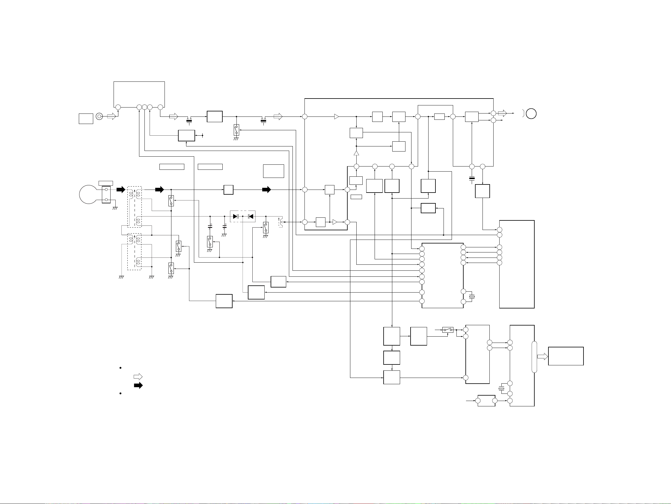
6-3. BLOCK DIAGRAM — TUNER SECTION —
TU1
TUNER UNIT
CNP2
EXT ANT
FM
ANT
1 5 8 6
VT
OSC OUT
VCC
IF OUT
7
CF1 CF2
FM B+SW
Q24
IF AMP
Q4
RADIO7.5V
IF MUTE
Q8
PMC-D407L
FM/AM RF AMP, OSC, IF AMP, DET
FM
IF IN
6
IF
BUFFER
FM
DET
IC1
FM/AM
BUFFER
AM
DET
DET
OUT
17 16
FM
MPX
L OUT
R OUT
R-CH
L-CH
A
TAPE SECTION
(Page 27)
11
12
MPX
T1
IN
MW/LW LOOP
ANTENNA
04
CNP1
MW/LW
CT5, L5
LW TRACKING
L3
MW RF
MW SW
L5
LW RF
Q3
Signal Path
: FM
: MW/LW
R-ch : same as L-CH.
LW SW
Q1
MW SW
Q2
MW TRACKING
CT5 CT4
LW
SW
Q5
MW SW
Q21
AMP
Q6
D5
LW
SW
Q7
VT
CONTROL
Q13
L4CT4, L3
LW
FREQUENCY
COVERAGE
L4
AM OSC
LW SW
Q22
ST-IND
XIN
CF4
7
CD
6
DA
5
CK
4
CE
1
2
5
12
4
5V
VCO
13 10
STEREO
SW
Q17
X1
75kHz
FM/MW DISPLAY
CONTROL
IC404
VDD1
VDD2
R DATA
R CLK
MUX
2.62MHz
RESET
IC402
2
16
X402
12
SYSTEM CONTROL
IC801 (1/3)
R ST
24
B MUTE
95
25
R COUNT
R DAT
26
27
R CLK
R CE
28
RDS LCD
CONTROL
6
DATA
5
CLK
EXTAL
29
XTAL
30
28
RESET
IC401
COM 0-3
SEG 0-31
36
|
69
•
74
•
75
LCD401
RADIO DATA SYSTEM
LIQUID CRYSTAL
DISPLAY PANEL
MO-ST
BAND
AM
IF IN
7
CFT1
AM
RF IN
24
AM
OSC
AM
22
OSC
AM
MIX
MIX
OUT
OSC
OUT
3
19
CFT1
AM IF
MONO-ST
SW
Q12
BAND
SW
Q10
RDS
CONTROL
SW
Q25,26
RDS
CONTROL
Q27
RDS
DETECT
Q28
IF OUT
181514
FM/LW
CONTROL
SW
Q407
14
13
9
16
8
17
10
21
11
AM
HI-CUT
Q9
IF SW
Q11
IF IN
P6
MO/ST
AM IN
FM
FM IN
LW
PD1
MW
PLL
IC2
XOUT
Q405
5V
– 23 – – 24 –
Page 24
PMC-D407L
6-4. BLOCK DIAGRAM — CD SECTION —
OPTICAL PICK-UP
KSS-213C
I-V
AMP
PD
LD
TRACKING
FOCUS
04
LD POWER
CONTROL
Q701, 703
M702
(SLED)
M701
(SPINDLE)
CD RF & SYSTEM SERVO PROCESSOR
RV703
E-F
BALANCE
RV702
FOCUS
GAIN
FOCUS/TRACKING COIL DRIVE,
SLED/SPINDLE MOTOR DRIVE
T+
T-
F+
F-
SL+
M
SL-
SP+
M
SP-
IC701
PD1 RF PCMD
35 31
36
PD2
39
E
38
F
40
EI
1
FO
2
FI
34
PD
33
LD
IC703
27
LEVEL
SHIFT
26
18
LEVEL
SHIFT
17
2
LEVEL
SHIFT
1
12
LEVEL
SHIFT
11
RFO
25
FOK
SENS
24
21
DATA
20
XLT
19
CLK
23 55
C.OUT
F.BIAS
TO
TI
XRST
SLO
FEO
TFO
MUTE
RV701
FOCUS
37
42
44
22
16
6
13
25
19
3
7
10
14
15
TIN
FIN
SLIN
SPIN
SPI
BIAS
RV704
TRACKING
GAIN
CD DIGITAL SIGNAL PROCESSOR
S701
(LIMIT)
IC702
14 21 6 12
EMPH
FOK
1
54
SEIN
DATO
56
57
XLTO
59
CLKO
CNIN
60
SPOA
50
XRST
64
LDON
MDP
3
40
22
BCK
20
LRCK
XTAI
34
XTAO
35
MUTE
48
39
DOUT
49 10
SENS
SCOR
43
46
SQSO
SQCK
47
51
DATA
52
XLAT
CLOK
53
X701
16.9344MHz
FREQUENCY
CONVERTER
Q802, 803
32.768kHz
S801
OPEN/CLOSE
X801
PUSH
5
8
18
1
22
SYSTEM CONTROL, LCD DRIVE
94
2
12
11
6
5
7
D802
4
D803
92
93
37
39
40
X802
4.19MHz
8
D/A CONVERTER
IC704
DATA LO
EMPH
BCK
LRCK
XI
MUTE
RSTN
C-MUTE COMO-3
C-SENS
C-SCOR
C-SQSO
C-SQCK
C-DATA
C-XLAT
C-CLK
C-XRST
TX
TEX
SFC
EXTAL1
XTAL1
C-DOOR
RO
IC801 (3/3)
SEG1-23
KEY0
KEY1
KEY2
KEY3
BL CONT
RMC
AC CHK
142
RST
50
77
31
32
33
34
88
38
|
3
1
BL7.5V
R-CH
OPTICAL
DIGITAL OUT
3
RESET
IC803
AC CHK
Q801
L-CH
(CD)
J331
LCD801
LIQUID CRYSTAL
DISPLAY PANEL
S901-923
KEY MATRIX
LCD BACK
LIGHT DRIVE
Q805
3
D805
21
Q804
REMOTE
CONTROL
RECEIVER
IC901
1
COM12V
TAPE SECTION
B
(Page 27)
PL801,802,
PL804,805
(LCD BACK LIGHT)
D804
+5V
3 2
REG
IC802
COM12V
Signal Path
: CD
: digital out
R-ch : same as L-CH.
– 25 – – 26 –
Page 25
6-5. BLOCK DIAGRAM — TAPE SECTION —
PMC-D407L
(Page 26)
(Page 24)
TUNER SECTION
(HEAD POSITION)
J323
LINE IN
B
CD SECTION
A
L-CH
R-CH
ERASE
HRPE101
PM691
PLUNGER
SOLENOID
S696
MODE
S691
HALF
(CASSETTE)
S694
REC-REV
(ERASE PROOF)
S695
REC-FWD
(ERASE PROOF)
(CAPSTAN/REEL)
04
L-CH
L-CH
M691
PH691
M
REF
R-CH
Q102
REC/PB
SW
Q302, 303
TC M.SW
Q311, 312
CD/LINE
MUTE
R-CH
R-CH
Q308
99
17
30
19
Q331, 332
T301
BL7.5V
D312
T END
T MODE
T STAT
T MCON
CONTROL
MUTE
CONTROL
Q333
REC/PB PRE AMP
SYSTEM CONTROL
IC801 (2/3)
Q131
Q132
L. CD
22
L. RAD
24 20 31 24
L. IN
5
L. RD
4
R. IN
8
R. RD
9
SOLENOID
DRIVE
Q309
BUFFER
Q310
Q317
Q325
REC/PB
SW
Q304, 305
COM12V
Q307
TC CONTROL
D317
CD5V
RADIO7.5V
D319
IC301
LOGIC
REC/PB
SW
Q324
BIAS
OSC
Q301
REC/PB
SW
Q326, 328
T AMST SOL
A MUTE
V CLK
V DAT
V CE
T BIAS
ISS1
ISS2
T REC
P CONT
L. LO
R. LO
TAPE
REC
BL7.5V
REC/PB
1816
96
21
22
23
13
97
98
15
20
18
15
21
SW
Q306
BL7.5V
MUTE
R-CH R-CH
AMS AMP DET
ELECTRONIC VOLUME
IC302
VOLTONE
DRIVER
12 13 14 15 18 19 20 21 23
Signal Path
: FM
: TAPE (PB)
: TAPE (REC)
: LINE IN
: CD
R-ch : same as L-CH.
IC305
COMP
CONTROL
BUFFER
Q604,605
BUFFER
Q606,607,608
Q101
Q104
IMPEDANCE USE 6Ω
Q103
F501 T501
F602
F603
Q609
R-CH
SPEAKER
OUT R-ch
J501
R-CH
RV601
LEVEL
T601
WOOFER AMP
IC601
ST/BY
3
7 6
V OUT
V IN
J332
LINE OUT
SP101
SPEAKER
L-CH
SP201
SPEAKER
R-CH
J301
(AC IN)
(AC IN)
F601
J602
AC OUTLET
MAX 35W
SP601
WOOFER
SPEAKER
J601
J303
SIGNAL
SIGNAL
OUTPUT
J502
SIGNAL INPUT
-1
L-1L
-2R-2
D305
H/P AMP
SW
Q334
Q319
BL7.5V
POWER
CONTROL
Q313
COM12V
TO
WOOFER AMP
INPUT
WOOFER
CD7.5VCOM5V
WOOFER
BUFFER
Q399
STANDBY
83
6
Q330
CD5V
D320
Q314
RADIO7.5V
R-CH
CD
+5V SW
Q320
VT
MUTE
Q398
J302
SIGNAL OUTPUT
MEGA BASS
Q329
BL7.5V
TU7.5V
SW
Q316
D307
R
+5V REG
LED
DRIVE
Q611
BUFFER
Q602,603
REG
B+
Q610
3 1
LINE AMP
IC304
3
2
POWER AMP
IC309
H/P AMP
IC303
7 1
VCC
2
MUTE
CONTROL
Q327, 335
CD +7.5V
REG
Q318
AUDIO
+7.5V REG
Q315
+12V REG
Q323
REG
B+
Q601
+18V
–18V
D611
POWER
MUTE
Q612,615
12
14
15
17
RECT
D501-504
D601-604
RECT
– 27 – – 28 –
Page 26
PMC-D407L
• Semiconductor
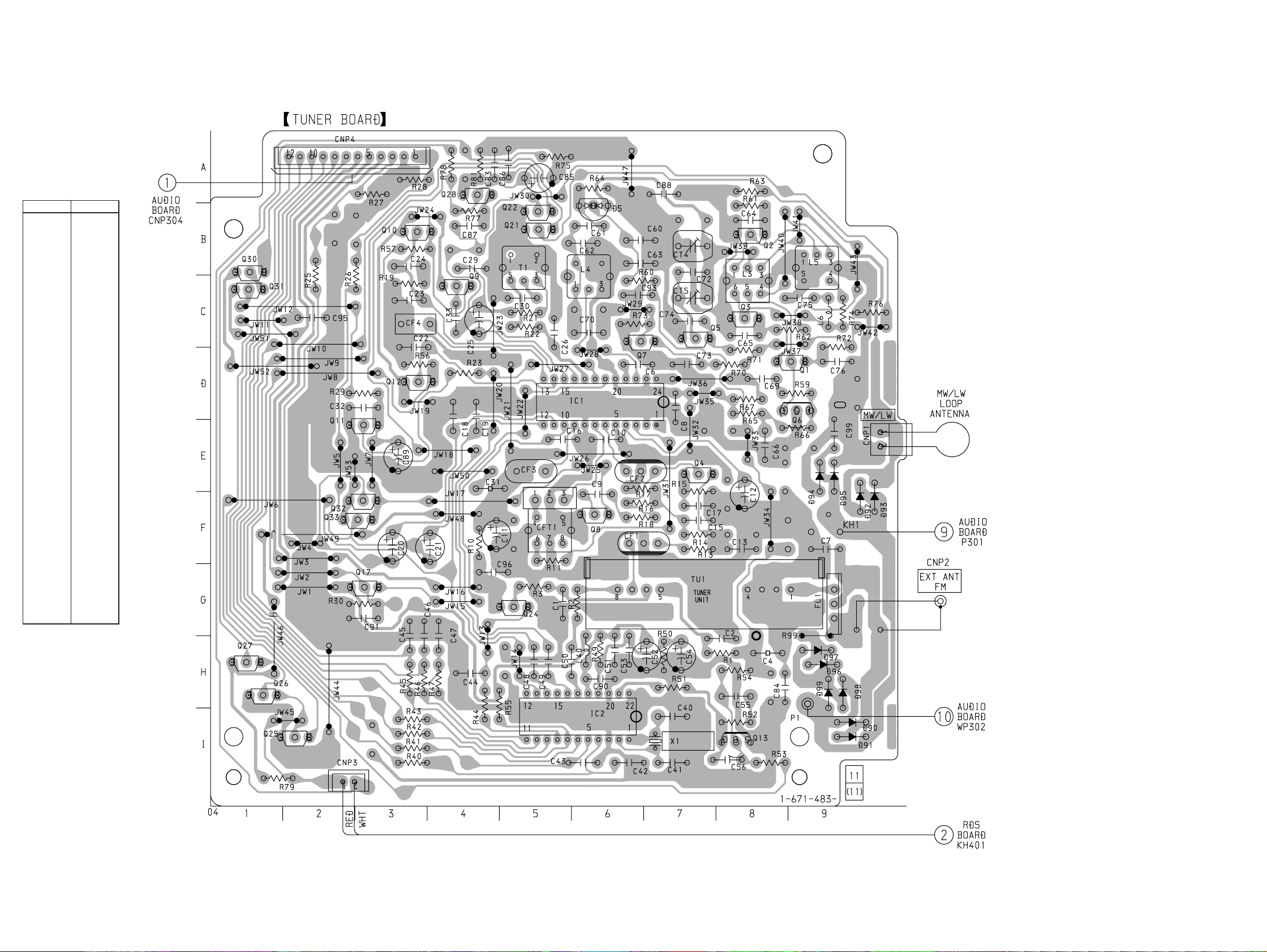
Location
Ref. No. Location
D5 B-6
D90 I-9
D91 I-9
D92 F-9
D93 F-9
D94 E-9
D95 E-9
D96 H-9
D97 H-9
D98 H-9
D99 H-9
IC1 E-6
IC2 H-6
Q1 D-8
Q2 B-8
Q3 C-8
Q4 E-7
Q5 C-7
Q6 D-9
Q7 C-6
Q8 F-6
Q9 C-4
Q10 B-3
Q11 E-3
Q12 D-3
Q13 I-8
Q17 G-3
Q21 B-5
Q22 B-5
Q24 G-5
Q25 I-2
Q26 H-1
Q27 H-1
Q28 A-4
Q30 B-1
Q31 C-1
Q32 F-3
Q33 F-2
6-6. PRINTED WIRING BOARD — TUNER SECTION — • Refer to page 21 for Circuit Boards Location.
(Page 44)
Note on Schematic Diagram:
• All capacitors are in µF unless otherwise noted. pF: µµF
50 WV or less are not indicated except for electrolytics
and tantalums.
• All resistors are in Ω and 1/
specified.
¢
•
: internal component.
4
W or less unless otherwise
• C : panel designation.
• U : B+ Line.
• H : adjustment for repair.
• Voltage and waveforms are dc with respect to ground
under no-signal (detuned) conditions.
no mark : FM
( ) : MW
< > : LW
• Voltages are tak en with a V OM (Input impedance 10 MΩ).
Voltage variations may be noted due to normal production tolerances.
• Waveforms are taken with a oscilloscope.
Voltage variations may be noted due to normal production tolerances.
• Circled numbers refer to waveforms.
• Signal path.
F : FM
f : MW/LW
(Page 44)
Note on Printed Wiring Boards:
• X : parts extracted from the component side.
• W : indicates side identified with part number.
¢
•
: internal component.
• b : Pattern from the side which enables seeing.
TP(VT)
(Page 44)
(Page 33)
– 29 – – 30 –
Page 27
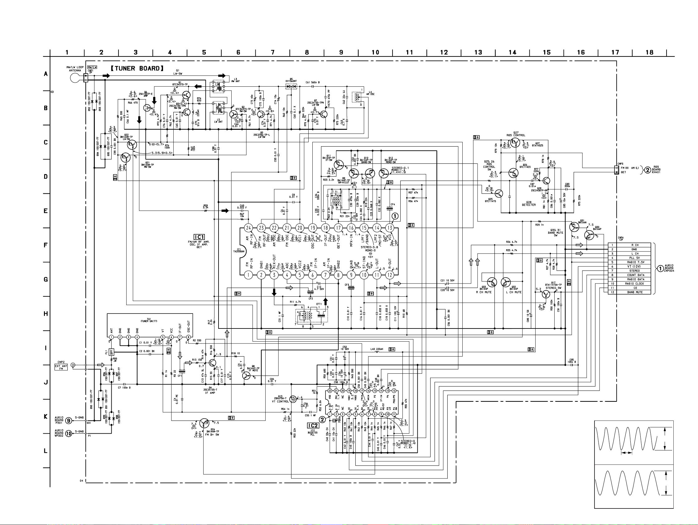
6-7. SCHEMATIC DIAGRAM — TUNER SECTION — • Refer to page 63 for IC Block Diagrams.
PMC-D407L
(Page 36)
(Page 47)
(Page 47)
• Waveforms
1
IC1
!£
(Page 46)
1.4Vp-p
2.2µs
(VCO)
– 31 – – 32 –
2
IC2
75kHz
(X OUT)
1
1.4Vp-p
Page 28
PMC-D407L
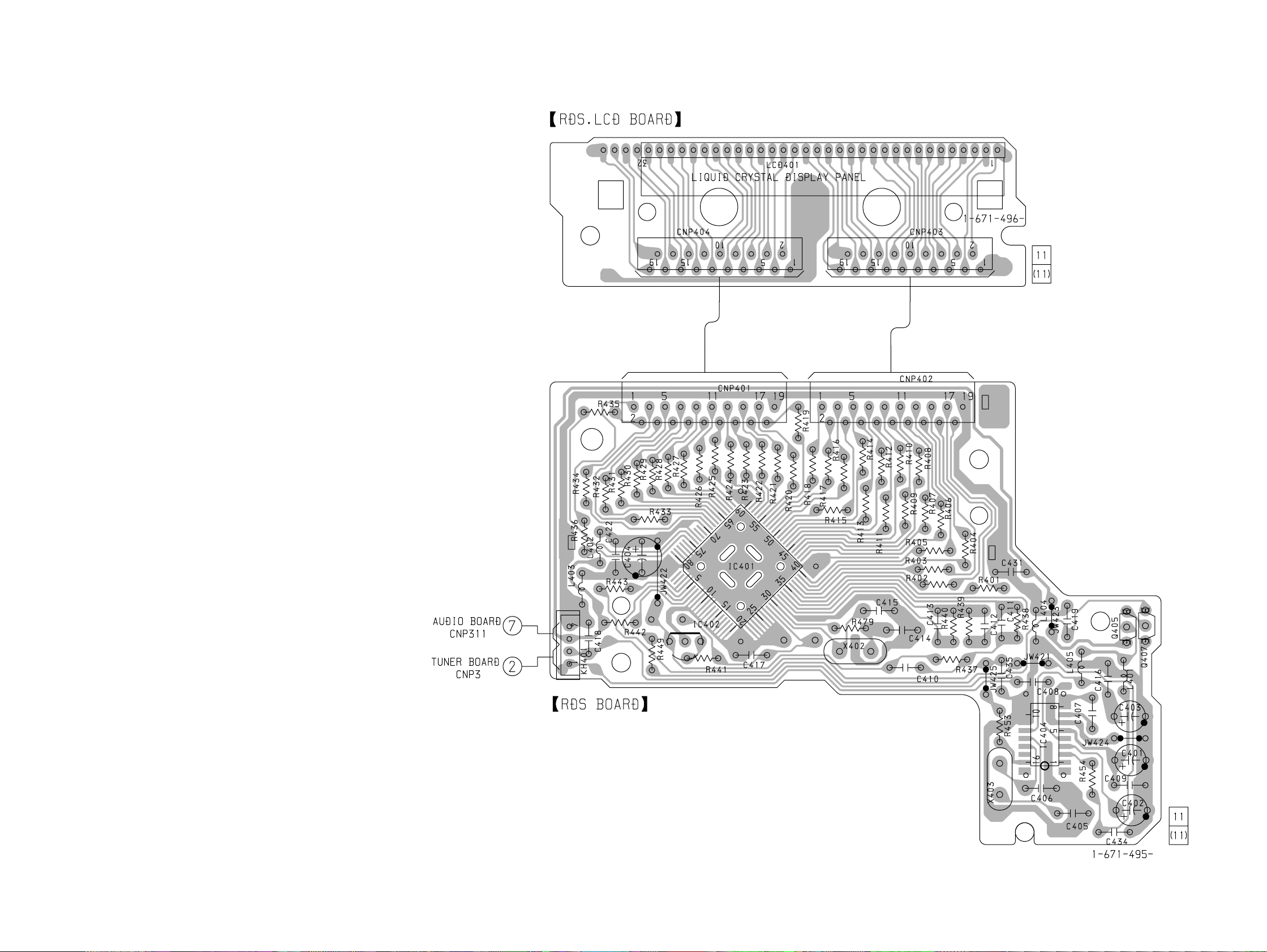
6-8. PRINTED WIRING BOARDS — RDS SECTION — • Refer to page 21 for Circuit Boards Location.
(Page 44)
13
(Page 30)
04
Note:
• X : parts extracted from the component side.
• b : Pattern from the side which enables seeing.
– 33 – – 34 –
Page 29
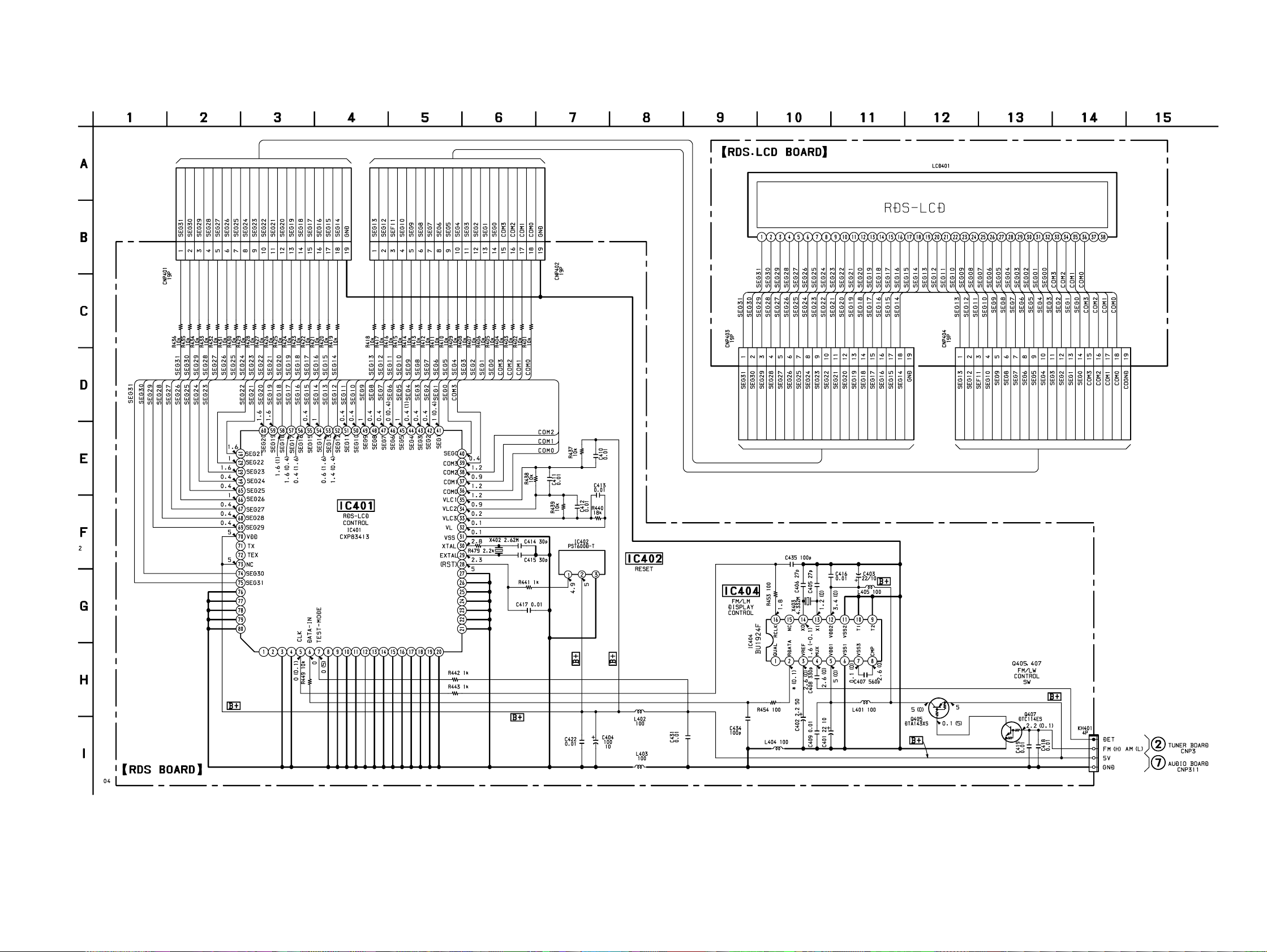
6-9. SCHEMATIC DIAGRAM — RDS SECTION — • Refer to page 64 for IC Block Diagrams.
PMC-D407L
Note:
• All capacitors are in µF unless otherwise noted. pF: µµF
50 WV or less are not indicated except for electrolytics
and tantalums.
• All resistors are in Ω and 1/
specified.
• U : B+ Line.
4
W or less unless otherwise
• Voltage is dc with respect to ground under no-signal
• V oltages are taken with a V OM (Input impedance 10 MΩ).
– 35 – – 36 –
(Page 32)
(Page 47)
(detuned) condition.
no mark : FM
( ) : MW
Voltage variations may be noted due to normal production tolerances.
Page 30
PMC-D407L
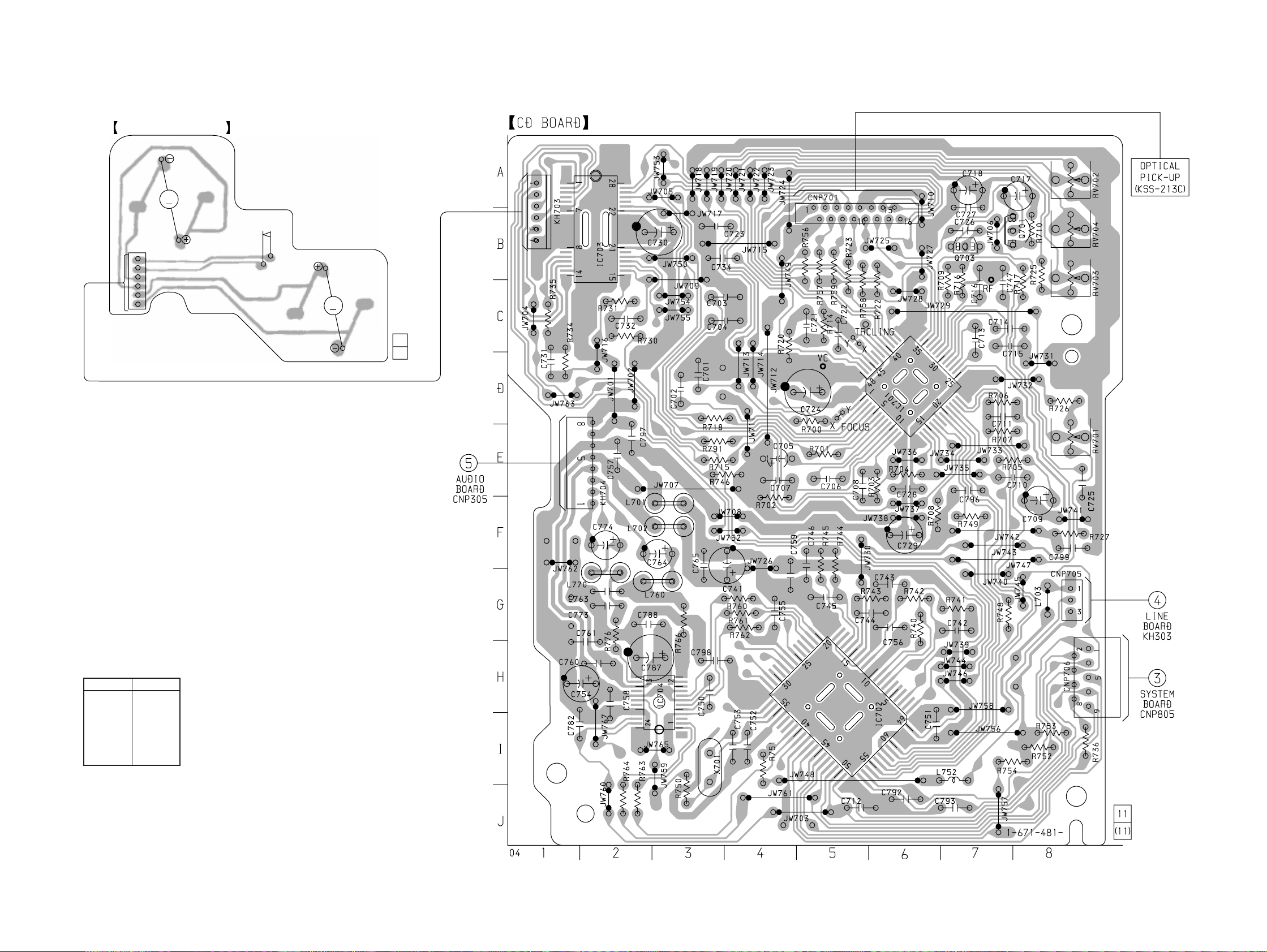
6-10. PRINTED WIRING BOARDS — CD SECTION — • Refer to page 21 for Circuit Boards Location.
CD MOTOR BOARD
M702
(SLED)
CNP707
6
1
M
S701
(LIMIT)
M701
(SPINDLE)
M
1-639-678-
12
(12)
(Page 44)
• Semiconductor
Location
Ref. No. Location
IC701 D-6
IC702 I-5
IC703 B-2
IC704 H-3
Q701 B-7
Q703 B-7
Note:
• X : parts extracted from the component side.
• b : Pattern from the side which enables seeing.
– 37 – – 38 –
(Page 43)
(Page 49)
Page 31

6-11. SCHEMATIC DIAGRAM — CD SECTION — • Refer to page 65 for IC Block Diagrams.
(Page 52)
• Wavef orms
1
IC701 #¡ (RFO)
2
IC701
3
IC701
4
IC702
5
1.3±0.2Vp-p
Approx. 50mVp-p
(TI)
$¢
Approx. 50mVp-p
(FI)
2
22.6µs
(LRCK)
@º
PMC-D407L
5Vp-p
6.7Vp-p
(Page 45)
(Page 46)
280ns
@™
(BCK)
IC702
6
4.8Vp-p
240ns
IC702
(XPCK)
@∞
7
4.8Vp-p
16.9344MHz
IC702
Note:
• All capacitors are in µF unless otherwise noted. pF: µµF
50 WV or less are not indicated except for electrolytics
and tantalums.
• All resistors are in Ω and 1/
specified.
Note: The components identified by mark ! or dotted line
with mark ! are critical for safety.
Replace only with part number specified.
• U : B+ Line.
• H : adjustment for repair.
• Voltage and waveforms are dc with respect to ground
under no-signal conditions.
no mark : CD STOP
• Voltages are tak en with a V OM (Input impedance 10 MΩ).
Voltage variations may be noted due to normal production tolerances.
• Waveforms are taken with a oscilloscope.
Voltage variations may be noted due to normal production tolerances.
• Circled numbers refer to waveforms.
• Signal path.
J : CD
c : digital out
(XTAO)
#∞
4
W or less unless otherwise
– 39 – – 40 – – 41 –
Page 32

PMC-D407L
6-12. PRINTED WIRING BOARDS — MAIN SECTION —
• Refer to page 21 for Circuit Boards Location.
SW BOARD
• Semiconductor
Location
Ref. No. Location
D301 H-7
D302 B-7
D304 C-5
D305 E-9
D307 A-7
D308 B-11
D309 C-10
D310 C-9
D311 B-9
D312 F-7
D313 B-9
D314 I-9
D315 B-8
D316 B-7
D317 D-5
D318 F-9
D319 D-8
D320 C-11
IC301 H-6
IC302 H-11
IC303 E-10
IC305 I-1
Q102 G-4
Q103 D-11
Q131 G-3
Q132 H-3
Q202 G-3
Q203 D-11
Q231 F-3
Q232 F-3
Q301 E-6
Q302 F-4
Q303 F-5
Q304 F-8
Q305 F-7
Q306 F-7
Q307 F-4
Q308 E-3
Q309 C-4
Q310 C-3
Q311 C-7
Q312 B-7
Q313 C-10
Q314 C-11
Q316 D-8
Q317 B-6
Q319 C-8
Q320 E-7
Q323 C-8
Q324 F-9
Q325 E-4
Q326 F-8
Q327 D-2
Q328 E-8
Q329 I-9
Q330 J-12
Q331 C-2
Q332 C-3
Q333 D-5
Q334 E-10
Q335 E-2
Q398 C-12
Q399 C-12
S695
REC-FWD
(ERASE PROOF)
PH691
S691
HALF
(CASSETTE)
HEAD BOARD
WHT
BLU
RED
BLK
YEL
R691
CN691
(HEAD POSITION)
841
S696
MODE
M691
(CAPSTAN/REEL)
(ERASE PROOF)
(Page 44)
S694
REC-REV
PM691
PLUNGER
SOLENOID
4
(Page 38)
1-662-742-
11
(Page 33)(Page 37)(Page 49)
(Page 43)
(Page 30)
(Page 59)
(Page 30)
Note:
• X : parts extracted from the component side.
• Y : parts extracted from the conductor side.
• b : Pattern from the side which enables seeing.
HRPE101
RECORD/PLAYBACK
/ERASE HEAD
WHT
BLK
RED
WHT
BLK
1-662-743-
11
(Page 29)
– 42 – – 43 – – 44 –
Page 33

6-13. SCHEMATIC DIAGRAM — MAIN SECTION — • Refer to page 64 for IC Block Diagrams.
PMC-D407L
(Page 31)
(Page 31)
(Page 45)
(Page 41)
Note:
• All capacitors are in µF unless otherwise noted. pF: µµF
50 WV or less are not indicated except for electrolytics
and tantalums.
• All resistors are in Ω and 1/
specified.
• C : panel designation.
• U : B+ Line.
• V oltages are dc with respect to ground under no-signal
(detuned) conditions.
no mark : FM
( ) : PB
< > : REC
[ ] : CD
• Voltages are tak en with a V OM (Input impedance 10 MΩ).
Voltage variations may be noted due to normal production tolerances.
• Signal path.
F : FM
E : PB
a : REC
L : LINE IN
J : CD
c : digital out
: Impossible to measure
∗
4
W or less unless otherwise
(Page 47)
(Page 32)
(Page 61)
(Page 36)
(Page 41)
(Page 51)
– 45 – – 46 – – 47 –
Page 34

PMC-D407L
• Semiconductor
Location
Ref. No. Location
D801 H-2
D802 B-4
D803 B-5
D804 B-6
D805 B-6
IC801 E-5
IC802 B-4
IC803 H-8
Q801 E-2
Q802 G-7
Q803 G-7
Q804 B-2
Q805 C-1
6-14. PRINTED WIRING BOARDS — CONTROL SECTION — • Refer to page 21 for Circuit Boards Location.
(Page 38)
Note:
• X : parts extracted from the component side.
• b : Pattern from the side which enables seeing.
(Page 43)
– 48 – – 49 – – 50 –
–
+
Page 35

6-15. SCHEMATIC DIAGRAM — CONTROL SECTION —
• Wavef orms
1
4.19MHz
IC801
2
32.768kHz
IC801
(XTAL1)
$º
(£
PMC-D407L
4.9Vp-p
3Vp-p
(TEX)
(Page 46)
1
2
Note:
• All capacitors are in µF unless otherwise noted. pF: µµF
50 WV or less are not indicated except for electrolytics
(Page 39)
and tantalums.
• All resistors are in Ω and 1/
specified.
• C : panel designation.
• U : B+ Line.
• V oltages and wa vef orms are dc with respect to ground
under no-signal (detuned) conditions.
no mark : FM
( ) : PB
< > : REC
[ ] : CD
• Voltages are tak en with a V OM (Input impedance 10 MΩ).
Voltage variations may be noted due to normal production tolerances.
• Waveforms are taken with a oscilloscope.
Voltage variations may be noted due to normal production tolerances.
• Circled numbers refer to waveforms.
4
W or less unless otherwise
– 51 – – 52 – – 53 –
Page 36

PMC-D407L
• Semiconductor
Location
Ref. No. Location
D606 K-3
D607 G-3
D608 G-3
D609 B-1
Q601 J-2
Q602 H-1
Q603 F-1
Q604 E-2
Q605 D-3
Q606 E-3
Q607 F-3
Q608 G-2
Q609 D-2
Q610 H-3
Q611 C-3
Q612 H-2
Q615 G-2
6-16. PRINTED WIRING BOARDS — WOOFER SPEAKER SECTION — • Refer to page 22 for Circuit Boards Location.
D609
Note:
• X : parts extracted from the component side.
• p : parts mounted on the conductor side.
• b : Pattern from the side which enables seeing.
04
– 54 – – 55 – – 56 –
Page 37

6-17. SCHEMATIC DIAGRAM — WOOFER SPEAKER SECTION — • Refer to page 64 for IC Block Diagrams.
PMC-D407L
– 57 – – 58 –
Note:
• All capacitors are in µF unless otherwise noted. pF: µµF
50 WV or less are not indicated except for electrolytics
and tantalums.
• All resistors are in Ω and 1/
specified.
• C : panel designation.
Note: The components identified by mark ! or dotted line
with mark ! are critical for safety.
Replace only with part number specified.
• U : B+ Line.
• Voltages and w av eforms are dc with respect to ground in
playback mode.
no mark : FM
• Voltages are tak en with a V OM (Input impedance 10 MΩ).
Voltage variations may be noted due to normal production tolerances.
4
W or less unless otherwise
Page 38

PMC-D407L
6-18. PRINTED WIRING BOARDS — POWER AMPLIFIER SECTION — • Refer to page 22 for Circuit Boards Location.
(Page 44)
04
Note:
• X : parts extracted from the component side.
• b : Pattern from the side which enables seeing.
– 59 – – 60 –
Page 39

6-19. SCHEMATIC DIAGRAM — POWER AMPLIFIER SECTION —
PMC-D407L
(Page 47)
Note:
• All capacitors are in µF unless otherwise noted. pF: µµF
50 WV or less are not indicated except for electrolytics
and tantalums.
• All resistors are in Ω and 1/
specified.
• 2 : nonflammable resistor.
• C : panel designation.
Note: The components identified by mark ! or dotted line
with mark ! are critical for safety.
Replace only with part number specified.
4
W or less unless otherwise
– 61 – – 62 –
• U : B+ Line.
• Voltage and waveforms are dc with respect to ground
under no-signal (detuned) conditions.
no mark : FM
• Voltages are tak en with a V OM (Input impedance 10 MΩ).
Voltage variations may be noted due to normal production tolerances.
• Signal path.
F : FM
Page 40

• IC Block Diagrams
IC1 TA2008AN
IC2 BU2615S
2
XIN
1
XOUT
16
FMIN
15
AMIN
AM
FM
IC301 TA2068N
222324
FM
FM
MIX
AM
OSC
OSC
AM
MIX
REFERENCE DIVIDER
PRESCALER MAIN COUNT
AGC
1/8DIV
FM
IF
BUFFBUFF
RF
RF
18 1314192021
IF
BUFFAFBUFF
AM
DET
LEVEL
AM
IF
PHASE
DET
ULLOCK
17 16
DET
BUFFER
P5
AM/FM
ST/MONO
SW
FM
DETSTDET
10 11 1298765431 2
15
LINE
IN1
INT
EXT
RADIO
FM MPX
19
11
18
17
20
MUTE
PD1
PD2/P5
VDD1
VDD2
VSS
23 22 21
15k
LINE
TAPE
BUF AMP
NAB
AMP1
ALC
NAB
NAB
OUT1
IN1
10k
6k
RADIO
A1
NF1
REC
PLAY
PRE
OUT1
2024
1k 1k
MONITOR
AMP
10k
10k
10k
10k
26dB
7dB
MUTE
BUF AMP
B1
10k 10k
ALC1
REC
AMP1
REF AMP
4 5 6321
IN1
REC
NAB
OUT1
VREF
LOGIC
ON
PRE
VCC
1819 14 13
7dB
ON
BUF AMP
ALC2
DET
2.1
GND
RADIO
LINE
RADIO
10k
10k
10k
1k
10k
OUT2
6k
BUF AMP
A2
MUTE
ON
IN2
10k
RADIO
TAPE
AMP2
NAB
NAB
OUT2
MONITOR
AMP
MUTE
B2
26dB
REC
AMP2
987 10 11 12
IN2
REC
NAB
NF2
TAPE
151617
LINE
TAPETAPE
10k
NAB
TAPE
LINE
OUT2
IN2
10k
MIC
AMP1
1k
MIC
MIC
IN
NF
IC305 BA338
VCC
OUT
NOISE FILTER
MUTING
GND
NFB
9 8 7 6 5 4 3 2 1
IN
PRE AMP
S
B+
R
F.F.
COMPARATOR
Q
COMPARATOR
COMPARATOR
IC601 TDA2052V
MUTE/
ST-BY
3 4 5 6 721
IN–
OUT
VDD
MUTE/
STANDBY
VEE
IN1+
IN2+
SENSE TIMING
PULSE WIDTH
IC404 BU1924F
SHIFT REGISTER LATCH
3
CE
1
4
CK
5
DA
6
CD
7
P0
8
P1
14
P2
I/O
CTL
20BIT COUNT
12109
P3
P4
P6
IF COUNT
CTL
IF IN
13
QUAL
RDATA
VREF
MUX
VDD1
VSS1
VSS3
CMP
2
3
4
5
6
7
8
DEFFERENTIAL
DECODER
ANTI-ALIASING
VREF
ANALOG
BIPHASE
DECODER
8TH SWITCHED
CAPACITOR FILTER
PLL
1187.5Hz
PLL
57KHz
RDS/ARI
COMPARATOR
CLOCK
&
DRIVER
DIGITAL
TEST
RCLK
16
(NC)
15
14
X2
X1
13
VDD2
12
11
VSS2
T1
10
T2
9
– 63 – – 64 –
Page 41

IC701 CXA1782BQ
PHD2
PHD1
35 34
PHD
–
+
+
–
36
LD
33
RF M
32
+
–
+
–
RF O
31
–
+
RF I
30
+
–
29CP28
CB
+
CC1
CC2
27
FOK
2526
–
APC
–
+
RF IV AMP1
–
FOK
LEVELS
–
+
+ +
+
–
––
MIRR
DFCT
24 SENS
IIL
+
–
TTL
23 C. OUT
22 XRST
+
RF IV AMP2
37FE BIAS
+
–
38F
–
FE AMP
TTL
IIL
• IIL DATA RESISTOR • INPUT SHIFT RESISTOR
• ADDRESS DECODER
• OUTPUT DECODER
TTL
21 DATA
20 XLT
IIL
19 CLK
+
F IV AMP
39E
–
+
+
40EI
E IV AMP
TE AMP
–
–
+
FZC COMP
–
+
BAL1
BAL2
BAL3
41VEE
42TEO
TOG1
TOG2
TOG3
43LPFI
44TEI
45ATSC
46TZC
47TDFCT
48VC
• WINDOW COMP
ATSC
DFCT
–
+
–
+
+
–
TZC COMP
DFCT
TM1
FS4
TOG1-3 FS1-4 TG1-2 TM1-7 PS1-4
BAL1-3
+
+
––
• TRACKING
TG1
FS1
• PHASE
COMPENSATION
HPF COMP LPF COMP
• FCS PHASE
COMPENSATION
FS2
+
–
TM7
TG2
TM6
TM5
TM4
TM3
• ISET
–
+
TM2
+
–
• F SET
18 VCC
17 ISET
16 SL 0
15 SL M
14 SL P
1312TA O
TG2
11
FSET
TA M
3
2
1
FEI
FEO
FDFCT
4
FGD
5
FLB
6
FE O
FE M
SRCH
TGU
9
8
7
10
– 65 –
Page 42

IC702 CXD2507AQ
XLON
SPOD
SPOC
SPOB
SPOA
CLKO
VDD
XLTO
DATO
CNIN
SEIN
CLOK
52535455565758596061626364
XLAT
FOK
MON
MDP
MDS
LOCK
TEST
FILO
FILI
PCO
VSS
AVSS
CLTV
AVDD
BIAS
ASYI
ASYO
ASYE
WDCK
1
2
3
4
5
6
7
8
9
10
11
12
13
14
RF
15
16
17
18
19
SERVO AUTO
SEQUENCER
14
INTERFACE
DIGITAL
PLL
ASYMMETRY
CORRECTOR
5
CPU
LRCK
PCMD
BCLK
5
DEMODULATOR
16K
RAM
XUGF
GTOP
SUB CODE
PROCESSOR
EFM
3
ERROR
CORRECTOR
3
VDD
XPCK
4
D/A
INTERFACE
GFS
RFCK
CZPO
DIGITAL
CLV
6
XROF
32313029282726252423222120
MNT3
DIGITAL
MNT1
OUT
CLOCK
GENERATOR
51
DATA
XRST
50
SENS
49
MUTE
48
SQCK
47
SQSO
46
45
EXCK
SBSO
44
SCOR
43
42
VSS
WFCK
41
EMPH
40
DOUT
39
C4M
38
37
FSTT
XTSL
36
XTAO
35
XTAI
34
33
MNTO
IC703 BA6898FP
GND
OUT4 –BOUT4 –AIN4
2728 26 25 24 23
D
D D
LEVEL SHIFT
LEVEL SHIFT
DD
21 3 4 5 6 7 8 9 10 11 12 13 14
IN1
OUT1 –B
OUT1 –A
T. S. D.
REGULATOR, BIAS,
RESET
IN4’
VREFIN
T. S. D. MONITOR
REG –B
REGOUT
22
VCC
VCC
MUTE
DRIVER
MUTE
VCC
VCC
IN3’
21 20 19
IN2’
GND
IN3
OUT3 –AOUT3 –BNC
18 17 16 15
D
LEVEL SHIFT
LEVEL SHIFT
DD
IN2
OUT2 –A
OUT2 –B
OPIN –B
NC
GND
OPOUT
– 66 –
Page 43

IC704 SM5877AM
MODE
ATCK
23
24
ATTENUATION COUNTER
1
MUTE
DS
RSTN
TIMING
CONTROL
R
R
NOISE SHAPER
L
L
3
CKO
PROCESSOR BLOCK
4
DVSS
FILTER PROCESSOR &
ATTENUATION PROCESSOR
2
DEEN
XVSS
202122
INPUT INTERFACE
5
6
DI
BCKI
10
15
TO1
AVDDR
11 12
AVDDL
RO
AVSS
14
13
LO
XVDD
L
BLOCK
PRODUCE
LRCI
TSTN
MUTE
16
17
XTI
XTO
19
18
R
PWN DATA
7
89
DVDD
– 67 –
Page 44

2
NOTE:
• The mechanical parts with no reference
number in the e xploded vie ws are not supplied.
• Items mar ked “*” are not stoc ked since
they are seldom required f or routine ser vice.
Some delay should be anticipated
when ordering these items.
• Abbreviation
IT : Italian model
CET : East European & CIS model
7-1. CASE SECTION
SECTION 7
EXPLODED VIEWS
• -XX and -X mean standardized parts, so
they ma y ha ve some diff erence from the
original one.
• Color Indication of Appear ance P arts
Example :
KNOB, BALANCE (WHITE) ... (RED)
N
Par ts Color Cabinet’ s Color
N
• Accessories and packing materials and
hardw are (# mar k) list are giv en in
the last of this parts list.
The components identified by
mark ! or dotted line with mark.
! are cr itical for saf ety.
Replace only with part number
specified.
cabinet (CD) section
not supplied
#1
cabinet (front)
section
10
#1
#8
9
#1
8
7
#2
4
#
#1
5
3
1
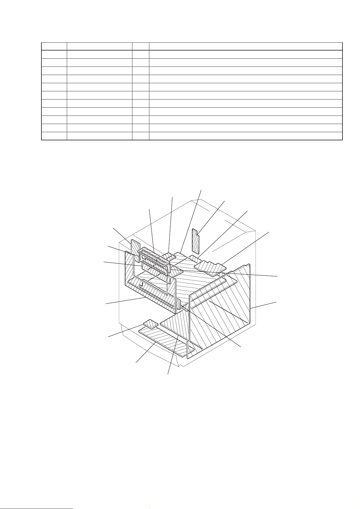
Ref. No. Part No. Description Remark
1 3-014-503-01 FOOT
* 2 A-3321-585-A TUNER BOARD, COMPLETE
3 1-782-296-11 WIRE, PARALLEL (FFC) (27 CORE)
4 3-014-125-01 CABINET (REAR)
* 5 A-3321-586-A AUDIO BOARD, COMPLETE
#1
#1
#1
2
6
1
Ref. No. Part No. Description Remark
6 3-014-127-01 CASE (LOWER)
7 3-031-341-01 SHEET, INSULATING (MAIN)
* 8 1-672-059-11 REGULATOR BOARD
* 9 3-031-261-01 COVER (MAIN), HEAT SINK
* 10 3-031-262-01 BRACKET (HEAT SINK)
– 68 –
Page 45

7-2. CABINET (FRONT) SECTION
53
54
55
56
#3
#3
#4
67
57
#3
58
#3
66
#3
#5
65
#1
MF-D307
59
#5
61
62
#1
#3
#6
60
63
64
52
Ref. No. Part No. Description Remark Ref. No. Part No. Description Remark
51 X-3373-799-1 LID (TERMINAL) ASSY
52 X-3376-240-1 LID ASSY, CASSETTE
53 X-3376-239-1 PANEL ASSY, FRONT
54 3-028-250-01 BUTTON (MAIN)
55 3-028-259-01 CABINET (FRONT)
56 3-014-092-01 BUTTON (UPPER)
* 57 1-671-486-11 SW2 BOARD
* 58 1-671-485-11 SW1 BOARD
59 3-014-097-01 PLATE (CASSETTE), LOCK
51
60 3-014-098-01 RETAINER (CASSETTE), LOCK
61 3-013-735-01 SPRING, COMPRESSION
62 3-014-100-01 HOLDER (TERMINAL)
* 63 A-3321-584-A LINE BOARD, COMPLETE
64 3-014-102-01 SPRING (CASSETTE)
65 3-014-096-01 HOLDER (CASSETTE)
66 3-014-103-01 SPRING (TERMINAL LID)
67 3-343-248-01 DAMPER (P), SMALL
– 69 –
Page 46

7-3. CABINET (CD) SECTION
#3
LCD401
125
104
#3
124
126
127
107
128
105
121
126
#3
#1
108
123
#3
109
#3
103
110
S801
106
113
114
111
112
#7
115
#3
LCD801
122
#3
#1
119
KSM-213CDM
116
120
102
117
117
#1
Ref. No. Part No. Description Remark Ref. No. Part No. Description Remark
* 101 A-3321-587-A CD BOARD, COMPLETE
102 1-782-294-11 WIRE, PARALLEL (FFC) (9 CORE)
* 103 A-3321-588-A SYSTEM BOARD, COMPLETE
* 104 1-671-487-11 H/P BOARD
* 105 1-671-497-11 LAMP1 BOARD
106 3-028-495-01 CHASSIS (CD)
107 3-014-129-01 WINDOW (CD)
108 3-351-377-11 DAMPER
109 3-014-128-01 SPRING (CD)
110 3-014-124-01 LID (CD)
101
117 3-916-006-01 SCREW (2.6X16)
* 118 1-639-678-12 CD MOTOR BOARD
119 3-931-379-01 RUBBER, VIBRATION PROOF
120 1-769-069-11 WIRE (FLAT TYPE) (16 CORE)
121 3-028-260-01 HOLDER, LCD
122 3-028-491-01 ILLUMINATOR
* 123 A-3321-617-A RDS BOARD, COMPLETE
124 3-028-490-01 ILLUMINATOR (RDS)
125 3-028-492-01 HOLDER (RDS), LCD
126 1-783-983-11 WIRE, PARALLEL (19 CORE)
118
111 1-452-732-11 MAGNET
112 3-910-112-01 PLATE (KSM-213-CDM), CHUCKING
113 3-014-131-01 LEVER
* 114 3-014-132-01 SPRING, COMPRESSION
115 3-910-116-01 COVER, CD
116 3-910-095-31 RUBBER, VIBRATION PROOF
* 127 1-671-496-11 RDS.LCD BOARD
* 128 1-671-498-11 LAMP2 BOARD
LCD401 1-803-161-11 DISPLAY PANEL, LIQUID CRYSTAL (RDS)
LCD801 1-803-162-11 DISPLAY PANEL, LIQUID CRYSTAL
S801 1-692-960-11 SWITCH, PUSH (1 KEY) (6 PUSH OPEN/CLOSE)
– 70 –
Page 47

7-4. OPTICAL PICK-UP SECTION
(KSM-213CDM)
154
155
not supplied
151
156
153
152
M701
M702
The components identified b y
mark ! or dotted line with mark.
! are cr itical for saf ety.
Replace only with part number
specified.
Ref. No. Part No. Description Remark Ref. No. Part No. Description Remark
151 2-627-003-02 GEAR (B) (RP)
152 X-2626-202-2 CHASSIS ASSY (MB), MOTOR (SPINDLE)
(INCLUDING M701)
153 2-626-908-01 SHAFT, SLED
! 154 8-848-483-08 PICK-UP, OPTICAL KSS-213C/Z-N
155 2-626-907-01 GEAR (A)
156 3-713-786-51 SCREW +P 2X3
M702 X-2625-769-1 GEAR ASSY (MB), MOTOR (SLED)
– 71 –
Page 48

7-5. TAPE MECHANISM DECK SECTION-1
(MF-D307)
214
209
211
208
HRPE101
207
212
210
205
216
215
213
217
206
204
222
223
220
221
218
227
203
202
226
201
Ref. No. Part No. Description Remark Ref. No. Part No. Description Remark
201 3-938-905-01 HEAD, LEVER
202 3-938-940-01 SPRING (L)
203 3-938-941-01 SCREW (A)
204 3-938-906-01 AZIMUTH, SPRING
205 3-017-432-01 SPRING (A)
224
225
219
* 215 3-938-916-01 BRAKE, ARM
* 216 3-938-914-01 FRAME (C)
* 217 3-938-913-01 FRAME (B)
* 218 3-938-909-01 LOCK, EJECT
219 3-938-944-01 SCREW (D)
206 3-938-901-01 HEAD, HOLDER
* 207 3-938-904-01 HEAD, FRAME
208 3-938-902-01 WASHER
209 3-938-903-01 SCREW
210 3-938-935-01 SPRING (G)
* 211 X-3372-610-1 ASSIST ASSY, LEVER
212 3-938-933-01 SPRING (E)
213 3-017-592-01 ARM (PINCH L) ASSY
214 3-938-934-01 SPRING (F)
220 3-017-591-01 ARM (PINCH R) ASSY
221 3-938-937-01 SPRING (I)
222 3-938-938-01 SPRING (J)
* 223 3-938-911-01 HEAD (B), CHASSIS
224 3-938-907-01 HEAD, GEAR ARM
225 3-938-943-01 SCREW (C)
226 3-938-942-01 SCREW (B)
* 227 1-662-743-11 HEAD BOARD
HRPE1011-500-480-11 HEAD, MAGNETIC (REC/PB/ERASE)
– 72 –
Page 49

7-6. TAPE MECHANISM DECK SECTION-2
(MF-D307)
255
259
257
258
256
261
254
262
255
260
253
263
252
PM691
251
264
265
266
not
supplied
267
275
268
286
285
269
270
273
274
275
282
261
276
284
M691
271
272
277
278
279
280
283
281
Ref. No. Part No. Description Remark Ref. No. Part No. Description Remark
251 3-938-949-01 WASHER (B)
252 3-938-951-01 WASHER (D)
253 3-938-936-01 SPRING (H)
254 3-938-930-01 SPRING (B)
255 3-938-910-01 REEL, CAP
* 256 3-938-912-01 ARM (UD)
257 3-938-952-01 WASHER (E)
258 3-938-948-01 WASHER (A)
259 3-938-932-01 SPRING (D)
260 3-938-908-01 CASSETTE, SPRING
261 3-938-945-01 SCREW (E)
262 3-017-428-01 FRAME (D)
263 3-938-920-01 PLUNGER, K
* 264 3-938-918-01 TRIGGER, ARM
265 3-938-931-01 SPRING (C)
266 3-938-921-01 GEAR (REEL)
* 267 1-662-742-11 SW BOARD
268 3-938-954-01 WASHER (G)
269 3-938-947-01 SCREW (G)
270 3-017-431-01 BRACKET (MM)
271 3-017-430-01 BELT
272 3-017-596-01 FLYWHEEL (R) ASSY
273 3-017-434-01 SCREW (H)
274 3-017-595-01 FLYWHEEL (L) ASSY
275 3-938-950-01 WASHER (C)
276 3-017-433-01 SPRING (K)
277 3-938-946-01 SCREW (F)
* 278 3-938-919-01 ARM (FR)
279 3-017-435-01 REFLECTOR
280 3-017-429-01 GEAR (REF)
281 3-938-917-01 GEAR (A)
282 3-938-924-01 GEAR (P)
283 3-938-923-01 GEAR (FR)
284 X-3372-613-1 CLUTCH ASSY
285 3-938-925-01 GEAR (IDL)
286 3-938-922-01 GEAR (CAM)
M691 3-016-425-01 MOTOR ASSY (CAPSTAN/REEL)
PM691 1-454-806-11 SOLENOID, PLUNGER
– 73 –
Page 50

7-7. SPEAKER (L) SECTION
306
#1
307
301
#1
#1
#1
308
305
302
303
317
304
303
316
#11
318
319
317
#9
309
SP101
#11
F501
#10
312
310
#10
321
315
320
#1
not supplied
not supplied
T501
311
#5
313
#5
311
314
The components identified b y
mark ! or dotted line with mark.
! are cr itical for saf ety.
Replace only with part number
specified.
Ref. No. Part No. Description Remark Ref. No. Part No. Description Remark
301 X-3376-076-1 SPEAKER (FRONT) SUB ASSY
302 3-028-031-01 BOX, SPEAKER (AEP)
302 3-028-031-11 BOX, SPEAKER (IT,CET)
303 3-365-853-01 SCREW (+BTPWH) (3X12)
304 3-028-028-01 DUCT (SPEAKER)
* 305 1-671-065-11 POWER AMP BOARD
* 306 1-671-066-11 TERMINAL BOARD
* 307 1-671-068-11 JACK BOARD
308 3-028-034-01 BRACKET (AMP)
309 3-028-029-01 CHASSIS (L), REAR
* 310 3-014-106-01 BUSHING (4P), CORD
311 3-029-171-01 SCREW, +B TAPPING
312 X-3374-496-1 CORD ASSY
313 3-703-244-11 BUSHING (2104), CORD
! 314 1-575-651-11 CORD, POWER
* 315 1-671-064-11 POWER BOARD
* 316 3-017-037-01 INSULATOR
317 3-568-749-00 CUSHION, ECM
318 4-812-134-11 RIVET (DIA. 3.5), NYLON
319 1-790-161-11 CORD, SPEAKER
320 3-028-032-01 COVER (HEAT SINK)
321 3-031-459-01 CUSHION (RT), RUBBER
! F501 1-532-505-31 FUSE, TIME-LAG (T5AL/250V)
SP101 1-505-607-11 SPEAKER (8cm) (L-CH)
! T501 1-433-453-11 TRANSFORMER, POWER (SET)
– 74 –
Page 51

7-8. SPEAKER (R) SECTION
357
356
358
354
353
355
#11
357
#11
SP201
353
352
351
Ref. No. Part No. Description Remark Ref. No. Part No. Description Remark
351 X-3376-076-1 SPEAKER (FRONT) SUB ASSY
352 3-028-031-01 BOX, SPEAKER (AEP)
352 3-028-031-11 BOX, SPEAKER (IT,CET)
353 3-365-853-01 SCREW (+BTPWH) (3X12)
354 3-028-028-01 DUCT (SPEAKER)
356 3-028-030-01 PANEL (R), REAR (AEP)
356 3-028-030-11 PANEL (R), REAR (IT,CET)
357 3-029-171-01 SCREW, +B TAPPING
358 3-014-109-01 STOPPER, CORD
SP201 1-505-607-11 SPEAKER (8cm) (R-CH)
355 1-790-161-11 CORD, SPEAKER
– 75 –
Page 52

7-9. WOOFER SPEAKER SECTION
403
402
404
409
not supplied
408
#1
407
427
426
428
#1
421
#1
405
#12
F601
not supplied
not supplied
410
429
412
421
406
423
412
SP601
#10
418
#10
422
T601
422
#1
#1
411
424
not supplied
425
423
not
supplied
F602
F603
417
416
425
415
#5
#5
#1
425
413
414
not
supplied
The components identified b y
401
420
419
425
Ref. No. Part No. Description Remark Ref. No. Part No. Description Remark
401 3-028-253-01 PANEL (SW)
402 3-028-255-01 BOX (SW), SPEAKER (AEP,CET)
402 3-028-255-11 BOX (SW), SPEAKER (IT)
403 3-028-254-01 KNOB, VOL
* 404 1-671-494-11 LEVEL BOARD
405 3-028-991-01 PACKING (WIRE)
406 3-028-992-01 PACKING (SPEAKER)
* 407 1-671-493-11 OUTLET BOARD
408 3-028-256-01 HOLDER (SW), AMP
* 409 A-3321-676-A S/WOOFER AMP BOARD, COMPLETE
* 410 1-672-061-11 S/WOOFER AMP2 BOARD
411 3-028-257-01 CHASSIS (SW), REAR
412 3-029-171-01 SCREW, +B TAPPING
413 3-703-244-11 BUSHING (2104), CORD
! 414 1-575-651-11 CORD, POWER
! 415 1-785-575-11 SOCKET, AC
* 416 1-672-060-11 AC OUTLET2 BOARD
* 417 1-671-492-11 WOOFER POWER BOARD
418 3-030-375-01 HOLDER, DUCT
419 3-028-252-01 DUCT (SW)
420 3-031-264-01 FOOT (SW)
421 3-029-240-01 CUSHION (4), SPEAKER
422 3-028-994-01 PACKING (2) (REAR)
423 3-028-993-01 PACKING (1) (REAR)
424 3-031-265-01 CUSHION, RUBBER (SW)
425 3-029-171-01 SCREW, +B TAPPING
426 3-031-572-01 CUSHION (VOL), RUBBER
427 3-031-459-01 CUSHION (PT), RUBBER
428 1-790-161-11 CORD, SPEAKER
429 3-031-669-01 SCREW, +BVPWH TAPPING
! F601 1-532-501-31 FUSE, TIME-LAG (T0.8AL/250V)
! F602 1-532-465-31 FUSE, TIME-LAG (T3.15AL/250V)
! F603 1-532-465-31 FUSE, TIME-LAG (T3.15AL/250V)
SP601 1-529-134-11 SPEAKER (WOOFER)
! T601 1-433-450-11 TRANSFORMER, POWER (SUPER WOOFER)
mark ! or dotted line with mark.
! are cr itical for saf ety.
Replace only with part number
specified.
– 76 –
Page 53

SECTION 8
ELECTRICAL PARTS LIST
NOTE:
• Due to standardization, replacements in
the par ts list ma y be different from the
par ts specified in the diag rams or the
components used on the set.
• -XX and -X mean standardized parts, so
they ma y ha ve some diff erence from the
original one.
• RESIST ORS
All resistors are in ohms.
MET AL:Metal-film resistor.
MET AL O XIDE: Metal o xide-film resistor .
F:nonflammable
Ref. No. Part No. Description Remark Ref. No. Part No. Description Remark
* 1-672-060-11 AC OUTLET2 BOARD
*****************
< CONNECTOR >
CNP607 1-564-321-00 PIN, CONNECTOR 2P
< AC SOCKET >
! J602 1-785-575-11 SOCKET, AC (AC OUTLET MAX 35V)
*************************************************************
• Items mar ked “*” are not stoc ked since
they are seldom required f or routine ser vice.
Some delay should be anticipated
when ordering these items.
• SEMICONDUCT ORS
In each case , u : µ, for example:
uA.. : µA.. uPA.. : µPA..
uPB.. : µPB.. uPC.. : µPC.. uPD.. : µPD..
• CAPACIT ORS
uF : µF
• COILS
uH : µH
C242 1-162-294-31 CERAMIC 0.001uF 10% 50V
C243 1-126-964-11 ELECT 10uF 20% 50V
C244 1-162-850-11 CERAMIC 0.082uF 10% 16V
C245 1-162-850-11 CERAMIC 0.082uF 10% 16V
C246 1-162-839-11 CERAMIC 0.01uF 10% 16V
C247 1-126-964-11 ELECT 10uF 20% 50V
C252 1-162-294-31 CERAMIC 0.001uF 10% 50V
C253 1-104-664-11 ELECT 47uF 20% 10V
C255 1-107-909-11 ELECT 47uF 20% 10V
C256 1-162-282-31 CERAMIC 100PF 10% 50V
AC OUTLET2
The components identified b y
mark ! or dotted line with mark.
! are cr itical for saf ety.
Replace only with part number
specified.
When indicating parts by reference
number , please include the board.
• Abbreviation
IT : Italian model
CET : East European & CIS model
AUDIO
* A-3321-586-A AUDIO BOARD, COMPLETE
**********************
7-685-871-01 SCREW +BVTT 3X6 (S)
< CAPACITOR >
C101 1-162-294-31 CERAMIC 0.001uF 10% 50V
C102 1-104-664-11 ELECT 47uF 20% 10V
C103 1-137-442-11 FILM 0.039uF 5% 50V
C104 1-162-302-11 CERAMIC 0.0022uF 20% 16V
C105 1-162-215-31 CERAMIC 47PF 5% 50V
C106 1-126-959-11 ELECT 0.47uF 20% 50V
C108 1-126-959-11 ELECT 0.47uF 20% 50V
C112 1-126-964-11 ELECT 10uF 20% 50V
C141 1-126-964-11 ELECT 10uF 20% 50V
C142 1-162-294-31 CERAMIC 0.001uF 10% 50V
C143 1-126-964-11 ELECT 10uF 20% 50V
C144 1-162-850-11 CERAMIC 0.082uF 10% 16V
C145 1-162-850-11 CERAMIC 0.082uF 10% 16V
C146 1-162-839-11 CERAMIC 0.01uF 10% 16V
C147 1-126-964-11 ELECT 10uF 20% 50V
C152 1-162-294-31 CERAMIC 0.001uF 10% 50V
C153 1-104-664-11 ELECT 47uF 20% 10V
C155 1-107-909-11 ELECT 47uF 20% 10V
C156 1-162-282-31 CERAMIC 100PF 10% 50V
C201 1-162-294-31 CERAMIC 0.001uF 10% 50V
C202 1-104-664-11 ELECT 47uF 20% 10V
C203 1-137-442-11 FILM 0.039uF 5% 50V
C204 1-162-302-11 CERAMIC 0.0022uF 20% 16V
C205 1-162-215-31 CERAMIC 47PF 5% 50V
C206 1-126-959-11 ELECT 0.47uF 20% 50V
C208 1-126-959-11 ELECT 0.47uF 20% 50V
C210 1-162-282-31 CERAMIC 100PF 10% 50V
C212 1-126-964-11 ELECT 10uF 20% 50V
C241 1-126-964-11 ELECT 10uF 20% 50V
C301 1-104-665-11 ELECT 100uF 20% 10V
C302 1-126-925-11 ELECT 470uF 20% 10V
C303 1-126-963-11 ELECT 4.7uF 20% 50V
C304 1-104-665-11 ELECT 100uF 20% 10V
C307 1-161-494-00 CERAMIC 0.022uF 25V
C311 1-162-305-11 CERAMIC 0.0068uF 30% 16V
C312 1-104-664-11 ELECT 47uF 20% 10V
C313 1-137-350-11 MYLAR 0.015uF 10% 100V
C314 1-162-294-31 CERAMIC 0.001uF 10% 50V
C315 1-162-305-11 CERAMIC 0.0068uF 30% 16V
C316 1-162-302-11 CERAMIC 0.0022uF 20% 16V
C324 1-126-961-11 ELECT 2.2uF 20% 50V
C325 1-126-961-11 ELECT 2.2uF 20% 50V
C326 1-126-963-11 ELECT 4.7uF 20% 50V
C327 1-104-664-11 ELECT 47uF 20% 10V
C328 1-126-959-11 ELECT 0.47uF 20% 50V
C329 1-137-189-11 FILM 0.18uF 5% 50V
C333 1-104-664-11 ELECT 47uF 20% 10V
C334 1-126-963-11 ELECT 4.7uF 20% 50V
C335 1-126-960-11 ELECT 1uF 20% 50V
C336 1-126-961-11 ELECT 2.2uF 20% 50V
C337 1-104-665-11 ELECT 100uF 20% 10V
C338 1-161-494-00 CERAMIC 0.022uF 25V
C339 1-161-494-00 CERAMIC 0.022uF 25V
C340 1-162-290-31 CERAMIC 470PF 10% 50V
C341 1-162-290-31 CERAMIC 470PF 10% 50V
C342 1-162-290-31 CERAMIC 470PF 10% 50V
C344 1-162-282-31 CERAMIC 100PF 10% 50V
C345 1-162-306-11 CERAMIC 0.01uF 30% 16V
C346 1-162-306-11 CERAMIC 0.01uF 30% 16V
C347 1-126-925-11 ELECT 470uF 20% 10V
C348 1-126-959-11 ELECT 0.47uF 20% 50V
C350 1-162-306-11 CERAMIC 0.01uF 30% 16V
C351 1-104-652-11 ELECT 470uF 20% 10V
C352 1-104-665-11 ELECT 100uF 20% 10V
– 77 –
Page 54

AUDIO
Ref. No. Part No. Description Remark Ref. No. Part No. Description Remark
C353 1-126-940-11 ELECT 330uF 20% 25V
C355 1-104-664-11 ELECT 47uF 20% 10V
C356 1-161-494-00 CERAMIC 0.022uF 25V
C357 1-104-665-11 ELECT 100uF 20% 10V
C358 1-161-494-00 CERAMIC 0.022uF 25V
JW121 1-410-397-21 FERRITE BEAD INDUCTOR 1.1uH
L154 1-410-397-21 FERRITE BEAD INDUCTOR 1.1uH
L254 1-410-397-21 FERRITE BEAD INDUCTOR 1.1uH
< FERRITE BEAD >
C359 1-126-964-11 ELECT 10uF 20% 50V
C360 1-161-494-00 CERAMIC 0.022uF 25V
C397 1-126-964-11 ELECT 10uF 20% 50V
C398 1-126-964-11 ELECT 10uF 20% 50V
C399 1-126-964-11 ELECT 10uF 20% 50V
< CONNECTOR >
* CNP301 1-564-709-11 PIN, CONNECTOR (SMALL TYPE) 7P
* CNP303 1-564-708-11 PIN, CONNECTOR (SMALL TYPE) 6P
CNP304 1-573-826-11 CONNECTOR, BOARD TO BOARD 12P
* CNP305 1-564-710-11 PIN, CONNECTOR (SMALL TYPE) 8P
CNP306 1-569-312-11 SOCKET, CONNECTOR (L TYRE) 27P
* CNP307 1-564-710-11 PIN, CONNECTOR (SMALL TYPE) 8P
* CNP309 1-779-536-11 PLUG, CONNECTOR 4P (POWER IN)
CNP310 1-564-707-11 PIN, CONNECTOR (SMALL TYPE) 5P
* CNP311 1-564-704-11 PIN, CONNECTOR (SMALL TYPE) 2P
< DIODE >
D301 8-719-991-33 DIODE 1SS133T-77
D302 8-719-991-33 DIODE 1SS133T-77
D304 8-719-991-33 DIODE 1SS133T-77
D305 8-719-991-33 DIODE 1SS133T-77
D307 8-719-991-33 DIODE 1SS133T-77
D308 8-719-991-33 DIODE 1SS133T-77
D309 8-719-991-33 DIODE 1SS133T-77
D310 8-719-991-33 DIODE 1SS133T-77
D311 8-719-110-09 DIODE RD8.2ES-B3
D312 8-719-991-33 DIODE 1SS133T-77
D313 8-719-109-89 DIODE RD5.6ESB2
D314 8-719-991-33 DIODE 1SS133T-77
D315 8-719-921-89 DIODE MTZJ-13C
D316 8-719-991-33 DIODE 1SS133T-77
D317 8-719-991-33 DIODE 1SS133T-77
D318 8-719-991-33 DIODE 1SS133T-77
D319 8-719-991-33 DIODE 1SS133T-77
D320 8-719-991-33 DIODE 1SS133T-77
< CONNECTOR >
* P301 1-564-187-00 PIN, CONNECTOR
* P302 1-564-187-00 PIN, CONNECTOR
< TRANSISTOR >
Q102 8-729-900-74 TRANSISTOR DTC143TS
Q103 8-729-036-86 TRANSISTOR KTC3203Y-AT
Q131 8-729-900-74 TRANSISTOR DTC143TS
Q132 8-729-900-74 TRANSISTOR DTC143TS
Q202 8-729-900-74 TRANSISTOR DTC143TS
Q203 8-729-036-86 TRANSISTOR KTC3203Y-AT
Q231 8-729-900-74 TRANSISTOR DTC143TS
Q232 8-729-900-74 TRANSISTOR DTC143TS
Q301 8-729-036-86 TRANSISTOR KTC3203Y-AT
Q302 8-729-036-86 TRANSISTOR KTC3203Y-AT
Q303 8-729-036-86 TRANSISTOR KTC3203Y-AT
Q304 8-729-422-57 TRANSISTOR UN4111
Q305 8-729-900-80 TRANSISTOR DTC114ES
Q306 8-729-900-80 TRANSISTOR DTC114ES
Q307 8-729-036-86 TRANSISTOR KTC3203Y-AT
Q308 8-729-119-78 TRANSISTOR 2SC2785-HFE
Q309 8-729-036-86 TRANSISTOR KTC3203Y-AT
Q310 8-729-900-80 TRANSISTOR DTC114ES
Q311 8-729-195-23 TRANSISTOR 2SA952
Q312 8-729-900-80 TRANSISTOR DTC114ES
Q313 8-729-119-76 TRANSISTOR 2SA1175-HFE
Q314 8-729-900-80 TRANSISTOR DTC114ES
Q316 8-729-119-76 TRANSISTOR 2SA1175-HFE
Q317 8-729-900-80 TRANSISTOR DTC114ES
Q319 8-729-011-92 TRANSISTOR 2SC2001TP-K1K2
Q320 8-729-195-23 TRANSISTOR 2SA952
Q323 8-729-265-52 TRANSISTOR 2SC2655
Q324 8-729-422-57 TRANSISTOR UN4111
Q325 8-729-119-78 TRANSISTOR 2SC2785-HFE
Q326 8-729-422-57 TRANSISTOR UN4111
< IC >
IC301 8-759-264-71 IC TA2068N
IC302 8-759-432-41 IC BH3854AS
IC303 8-759-701-54 IC NJM2073D
IC305 8-759-905-47 IC BA338
< JACK >
J302 1-770-612-12 JACK, PIN 2P (SIGNAL OUTPUT)
J303 1-784-910-31 JACK, PIN 1P (SIGNAL OUTPUT WOOFER)
Q327 8-729-900-80 TRANSISTOR DTC114ES
Q328 8-729-900-80 TRANSISTOR DTC114ES
Q329 8-729-194-57 TRANSISTOR 2SC945-P
Q330 8-729-194-57 TRANSISTOR 2SC945-P
Q331 8-729-900-80 TRANSISTOR DTC114ES
Q332 8-729-422-57 TRANSISTOR UN4111
Q333 8-729-422-57 TRANSISTOR UN4111
Q334 8-729-119-76 TRANSISTOR 2SA1175-HFE
Q335 8-729-422-57 TRANSISTOR UN4111
Q398 8-729-119-78 TRANSISTOR 2SC2785-HFE
Q399 8-729-119-78 TRANSISTOR 2SC2785-HFE
– 78 –
Page 55

AUDIO
Ref. No. Part No. Description Remark Ref. No. Part No. Description Remark
< RESISTOR >
R101 1-249-431-11 CARBON 15K 5% 1/4W
R102 1-249-404-00 CARBON 82 5% 1/4W
R103 1-249-441-11 CARBON 100K 5% 1/4W
R104 1-247-843-11 CARBON 3.3K 5% 1/4W
R110 1-247-807-11 CARBON 100 5% 1/4W
R111 1-247-887-00 CARBON 220K 5% 1/4W
R112 1-249-437-11 CARBON 47K 5% 1/4W
R114 1-249-417-11 CARBON 1K 5% 1/4W
R115 1-249-417-11 CARBON 1K 5% 1/4W
R116 1-249-437-11 CARBON 47K 5% 1/4W
R127 1-249-437-11 CARBON 47K 5% 1/4W
R140 1-249-425-11 CARBON 4.7K 5% 1/4W
R145 1-249-429-11 CARBON 10K 5% 1/4W
R146 1-249-417-11 CARBON 1K 5% 1/4W
R151 1-249-429-11 CARBON 10K 5% 1/4W
R152 1-249-425-11 CARBON 4.7K 5% 1/4W
R153 1-249-417-11 CARBON 1K 5% 1/4W
R155 1-247-887-00 CARBON 220K 5% 1/4W
R156 1-249-425-11 CARBON 4.7K 5% 1/4W
R201 1-249-431-11 CARBON 15K 5% 1/4W
R202 1-249-404-00 CARBON 82 5% 1/4W
R203 1-249-441-11 CARBON 100K 5% 1/4W
R204 1-247-843-11 CARBON 3.3K 5% 1/4W
R210 1-247-807-11 CARBON 100 5% 1/4W
R211 1-247-887-00 CARBON 220K 5% 1/4W
R212 1-249-437-11 CARBON 47K 5% 1/4W
R214 1-249-417-11 CARBON 1K 5% 1/4W
R215 1-249-417-11 CARBON 1K 5% 1/4W
R216 1-249-437-11 CARBON 47K 5% 1/4W
R227 1-249-437-11 CARBON 47K 5% 1/4W
R240 1-249-425-11 CARBON 4.7K 5% 1/4W
R245 1-249-429-11 CARBON 10K 5% 1/4W
R246 1-249-417-11 CARBON 1K 5% 1/4W
R251 1-249-429-11 CARBON 10K 5% 1/4W
R252 1-249-425-11 CARBON 4.7K 5% 1/4W
R253 1-249-417-11 CARBON 1K 5% 1/4W
R255 1-247-887-00 CARBON 220K 5% 1/4W
R256 1-249-425-11 CARBON 4.7K 5% 1/4W
R301 1-247-903-00 CARBON 1M 5% 1/4W
R302 1-249-441-11 CARBON 100K 5% 1/4W
R303 1-249-429-11 CARBON 10K 5% 1/4W
R304 1-249-429-11 CARBON 10K 5% 1/4W
R305 1-249-421-11 CARBON 2.2K 5% 1/4W
R306 1-249-429-11 CARBON 10K 5% 1/4W
R307 1-247-807-11 CARBON 100 5% 1/4W
R311 1-249-389-11 CARBON 4.7 5% 1/4W
R312 1-249-439-11 CARBON 68K 5% 1/4W
R313 1-249-389-11 CARBON 4.7 5% 1/4W
R314 1-249-429-11 CARBON 10K 5% 1/4W
R315 1-249-429-11 CARBON 10K 5% 1/4W
R316 1-249-425-11 CARBON 4.7K 5% 1/4W
R317 1-247-807-11 CARBON 100 5% 1/4W
R318 1-249-435-11 CARBON 33K 5% 1/4W
R319 1-247-895-00 CARBON 470K 5% 1/4W
R320 1-247-903-00 CARBON 1M 5% 1/4W
R323 1-249-425-11 CARBON 4.7K 5% 1/4W
R324 1-249-417-11 CARBON 1K 5% 1/4W
R325 1-249-417-11 CARBON 1K 5% 1/4W
R327 1-249-417-11 CARBON 1K 5% 1/4W
R328 1-249-417-11 CARBON 1K 5% 1/4W
R329 1-249-417-11 CARBON 1K 5% 1/4W
R331 1-247-863-00 CARBON 22K 5% 1/4W
R332 1-249-437-11 CARBON 47K 5% 1/4W
R334 1-249-429-11 CARBON 10K 5% 1/4W
R335 1-249-425-11 CARBON 4.7K 5% 1/4W
R336 1-249-401-11 CARBON 47 5% 1/4W
R337 1-249-437-11 CARBON 47K 5% 1/4W
R338 1-249-417-11 CARBON 1K 5% 1/4W
R339 1-249-417-11 CARBON 1K 5% 1/4W
R340 1-249-417-11 CARBON 1K 5% 1/4W
R342 1-249-425-11 CARBON 4.7K 5% 1/4W
R343 1-249-429-11 CARBON 10K 5% 1/4W
R344 1-249-429-11 CARBON 10K 5% 1/4W
R345 1-249-441-11 CARBON 100K 5% 1/4W
R347 1-249-401-11 CARBON 47 5% 1/4W
R349 1-249-435-11 CARBON 33K 5% 1/4W
R351 1-249-401-11 CARBON 47 5% 1/4W
R352 1-249-428-11 CARBON 8.2K 5% 1/4W
R353 1-249-417-11 CARBON 1K 5% 1/4W
R355 1-247-885-00 CARBON 180K 5% 1/4W
R356 1-249-437-11 CARBON 47K 5% 1/4W
R357 1-249-421-11 CARBON 2.2K 5% 1/4W
R360 1-249-441-11 CARBON 100K 5% 1/4W
R361 1-247-815-00 CARBON 220 5% 1/4W
R362 1-247-807-11 CARBON 100 5% 1/4W
R363 1-249-441-11 CARBON 100K 5% 1/4W
R364 1-249-413-11 CARBON 470 5% 1/4W
R367 1-247-807-11 CARBON 100 5% 1/4W
R368 1-249-413-11 CARBON 470 5% 1/4W
R369 1-247-807-11 CARBON 100 5% 1/4W
R370 1-249-441-11 CARBON 100K 5% 1/4W
R371 1-249-421-11 CARBON 2.2K 5% 1/4W
R376 1-249-421-11 CARBON 2.2K 5% 1/4W
R377 1-249-421-11 CARBON 2.2K 5% 1/4W
R378 1-247-807-11 CARBON 100 5% 1/4W
R379 1-247-815-00 CARBON 220 5% 1/4W
R390 1-249-437-11 CARBON 47K 5% 1/4W
R391 1-249-437-11 CARBON 47K 5% 1/4W
R392 1-249-429-11 CARBON 10K 5% 1/4W
R393 1-249-429-11 CARBON 10K 5% 1/4W
R394 1-249-425-11 CARBON 4.7K 5% 1/4W
R395 1-247-843-11 CARBON 3.3K 5% 1/4W
R396 1-249-413-11 CARBON 470 5% 1/4W
R397 1-247-807-11 CARBON 100 5% 1/4W
– 79 –
Page 56

AUDIO
Ref. No. Part No. Description Remark Ref. No. Part No. Description Remark
R398 1-249-429-11 CARBON 10K 5% 1/4W
R399 1-249-429-11 CARBON 10K 5% 1/4W
T301 1-429-820-11 TRANSFORMER, BIAS OSCILLATION
*************************************************************
* A-3321-587-A CD BOARD, COMPLETE
C701 1-162-302-11 CERAMIC 0.0022uF 30% 16V
C702 1-136-165-00 FILM 0.1uF 5% 50V
C703 1-136-165-00 FILM 0.1uF 5% 50V
C704 1-136-165-00 FILM 0.1uF 5% 50V
C705 1-131-375-00 TANTALUM 4.7uF 10% 10V
C706 1-136-159-00 FILM 0.033uF 5% 50V
C707 1-136-156-00 FILM 0.018uF 5% 50V
C708 1-162-199-31 CERAMIC 10PF 5% 50V
C709 1-126-162-11 ELECT 3.3uF 20% 50V
C710 1-136-495-11 FILM 0.068uF 5% 50V
C711 1-162-215-31 CERAMIC 47PF 5% 50V
C712 1-162-306-11 CERAMIC 0.01uF 30% 16V
C713 1-136-159-00 FILM 0.033uF 5% 50V
C714 1-162-306-11 CERAMIC 0.01uF 30% 16V
C715 1-136-159-00 FILM 0.033uF 5% 50V
C716 1-136-165-00 FILM 0.1uF 5% 50V
C717 1-104-664-11 ELECT 47uF 20% 10V
C718 1-126-964-11 ELECT 10uF 20% 50V
C721 1-130-491-00 MYLAR 0.047uF 5% 50V
C722 1-161-494-00 CERAMIC 0.022uF 25V
C723 1-130-495-00 MYLAR 0.1uF 5% 50V
C724 1-128-241-11 ELECT 220uF 20% 10V
C725 1-162-199-31 CERAMIC 10PF 5% 50V
C726 1-162-294-31 CERAMIC 0.001uF 10% 50V
C727 1-162-306-11 CERAMIC 0.01uF 30% 16V
C728 1-162-306-11 CERAMIC 0.01uF 30% 16V
C729 1-124-589-11 ELECT 47uF 20% 16V
C730 1-104-652-11 ELECT 470uF 20% 10V
C731 1-162-305-11 CERAMIC 0.0068uF 30% 16V
C732 1-130-299-00 FILM 0.012uF 5% 50V
C734 1-162-305-11 CERAMIC 0.0068uF 30% 16V
C741 1-124-589-11 ELECT 47uF 20% 16V
C742 1-137-194-00 FILM 0.47uF 5% 50V
C743 1-162-290-31 CERAMIC 470PF 10% 50V
C744 1-162-286-21 CERAMIC 220PF 10% 50V
CD
< TRANSFORMER >
*******************
< CAPACITOR >
C754 1-124-589-11 ELECT 47uF 20% 16V
C755 1-162-306-11 CERAMIC 0.01uF 30% 16V
C756 1-162-306-11 CERAMIC 0.01uF 30% 16V
C757 1-162-306-11 CERAMIC 0.01uF 30% 16V
C758 1-162-306-11 CERAMIC 0.01uF 30% 16V
C759 1-162-306-11 CERAMIC 0.01uF 30% 16V
C760 1-162-306-11 CERAMIC 0.01uF 30% 16V
C761 1-162-306-11 CERAMIC 0.01uF 30% 16V
C763 1-162-600-11 CERAMIC 0.0047uF 30% 16V
C764 1-124-259-11 ELECT 4.7uF 20% 16V
C765 1-162-306-11 CERAMIC 0.01uF 30% 16V
C773 1-162-600-11 CERAMIC 0.0047uF 30% 16V
C774 1-124-259-11 ELECT 4.7uF 20% 16V
C782 1-162-294-31 CERAMIC 0.001uF 10% 50V
C787 1-128-241-11 ELECT 220uF 20% 10V
C788 1-162-306-11 CERAMIC 0.01uF 30% 16V
C792 1-162-290-31 CERAMIC 470PF 10% 50V
C793 1-162-290-31 CERAMIC 470PF 10% 50V
C796 1-162-306-11 CERAMIC 0.01uF 30% 16V
C797 1-162-294-31 CERAMIC 0.001uF 10% 50V
C798 1-162-294-31 CERAMIC 0.001uF 10% 50V
C799 1-162-306-11 CERAMIC 0.01uF 30% 16V
< CONNECTOR >
* CNP701 1-779-466-11 CONNECTOR, FFC/FPC 16P
* CNP705 1-564-719-11 PIN, CONNECTOR (SMALL TYPE) 3P
CNP706 1-691-068-21 HOUSING, CONNECTOR 9P
< IC >
IC701 8-752-074-34 IC CXA1782CQ
IC702 8-752-372-94 IC CXD2507AQ
IC703 8-759-473-42 IC BA6898FP
IC704 8-759-426-44 IC 27C512-C35A65-V3.03
< COIL >
L701 1-410-397-21 FERRITE BEAD INDUCTOR 1.1uH
L702 1-410-397-21 FERRITE BEAD INDUCTOR 1.1uH
L752 1-410-324-11 INDUCTOR 4.7uH
L760 1-410-397-21 FERRITE BEAD INDUCTOR 1.1uH
L770 1-410-397-21 FERRITE BEAD INDUCTOR 1.1uH
< TRANSISTOR >
Q701 8-729-195-23 TRANSISTOR 2SA952
Q703 8-729-900-74 TRANSISTOR DTC143TS
< RESISTOR >
C745 1-136-169-00 FILM 0.22uF 5% 50V
C746 1-162-306-11 CERAMIC 0.01uF 30% 16V
C747 1-137-370-11 FILM 0.01uF 5% 50V
C750 1-162-306-11 CERAMIC 0.01uF 30% 16V
C751 1-162-306-11 CERAMIC 0.01uF 30% 16V
C752 1-162-201-31 CERAMIC 12PF 5% 50V
C753 1-162-203-31 CERAMIC 15PF 5% 50V
R700 1-249-429-11 CARBON 10K 5% 1/4W
R701 1-249-440-11 CARBON 82K 5% 1/4W
R702 1-247-896-11 CARBON 510K 5% 1/4W
R703 1-249-441-11 CARBON 100K 5% 1/4W
R704 1-247-883-00 CARBON 150K 5% 1/4W
R705 1-249-437-11 CARBON 47K 5% 1/4W
R706 1-247-876-11 CARBON 75K 5% 1/4W
– 80 –
Page 57

CD HEAD
Ref. No. Part No. Description Remark Ref. No. Part No. Description Remark
R707 1-249-432-11 CARBON 18K 5% 1/4W
R708 1-247-883-00 CARBON 150K 5% 1/4W
R709 1-247-862-11 CARBON 20K 5% 1/4W
R710 1-249-393-11 CARBON 10 5% 1/4W
R714 1-247-883-00 CARBON 150K 5% 1/4W
R715 1-249-430-11 CARBON 12K 5% 1/4W
R716 1-249-430-11 CARBON 12K 5% 1/4W
R717 1-249-429-11 CARBON 10K 5% 1/4W
R718 1-247-899-11 CARBON 680K 5% 1/4W
R720 1-247-891-00 CARBON 330K 5% 1/4W
CD MOTOR JACKH/P
< VIBRATOR >
X701 1-767-226-11 VIBRATOR, CRYSTAL (16.9344MHz)
*************************************************************
* 1-639-678-12 CD MOTOR BOARD
****************
< CONNECTOR >
CNP707 1-564-722-11 PIN, CONNECTOR (SMALL TYPE) 6P
R722 1-249-439-11 CARBON 68K 5% 1/4W
R723 1-249-440-11 CARBON 82K 5% 1/4W
R725 1-249-437-11 CARBON 47K 5% 1/4W
R726 1-249-429-11 CARBON 10K 5% 1/4W
R727 1-249-429-11 CARBON 10K 5% 1/4W
R730 1-249-435-11 CARBON 33K 5% 1/4W
R731 1-247-863-00 CARBON 22K 5% 1/4W
R734 1-249-437-11 CARBON 47K 5% 1/4W
R735 1-249-429-11 CARBON 10K 5% 1/4W
R736 1-249-417-11 CARBON 1K 5% 1/4W
R740 1-247-843-11 CARBON 3.3K 5% 1/4W
R741 1-249-417-11 CARBON 1K 5% 1/4W
R742 1-249-429-11 CARBON 10K 5% 1/4W
R743 1-247-903-00 CARBON 1M 5% 1/4W
R744 1-247-887-00 CARBON 220K 5% 1/4W
R745 1-249-429-11 CARBON 10K 5% 1/4W
R746 1-249-437-11 CARBON 47K 5% 1/4W
R748 1-249-429-11 CARBON 10K 5% 1/4W
R749 1-249-429-11 CARBON 10K 5% 1/4W
R750 1-249-413-11 CARBON 470 5% 1/4W
R751 1-247-807-11 CARBON 100 5% 1/4W
R752 1-249-429-11 CARBON 10K 5% 1/4W
R753 1-249-429-11 CARBON 10K 5% 1/4W
R754 1-249-429-11 CARBON 10K 5% 1/4W
R756 1-249-440-11 CARBON 82K 5% 1/4W
R757 1-249-439-11 CARBON 68K 5% 1/4W
R758 1-249-439-11 CARBON 68K 5% 1/4W
R759 1-249-439-11 CARBON 68K 5% 1/4W
R760 1-249-417-11 CARBON 1K 5% 1/4W
R761 1-249-417-11 CARBON 1K 5% 1/4W
R762 1-249-417-11 CARBON 1K 5% 1/4W
R763 1-249-417-11 CARBON 1K 5% 1/4W
R764 1-249-417-11 CARBON 1K 5% 1/4W
R766 1-249-417-11 CARBON 1K 5% 1/4W
R776 1-249-417-11 CARBON 1K 5% 1/4W
R791 1-247-843-11 CARBON 3.3K 5% 1/4W
< SWITCH >
S701 1-572-085-11 SWITCH, LEAF (LIMIT)
*************************************************************
* 1-671-487-11 H/P BOARD
**********
< CAPACITOR >
C154 1-162-294-31 CERAMIC 0.001uF 10% 50V
C254 1-162-294-31 CERAMIC 0.001uF 10% 50V
< JACK >
J301 1-566-891-11 JACK (2)
< COIL >
L151 1-247-807-31 CARBON 100 5% 1/4W
L251 1-247-807-31 CARBON 100 5% 1/4W
L351 1-414-142-11 INDUCTOR 1uH
*************************************************************
* 1-662-743-11 HEAD BOARD
***********
*************************************************************
* 1-671-068-11 JACK BOARD
***********
< CAPACITOR >
C186 1-162-282-31 CERAMIC 100PF 10% 50V
C286 1-162-282-31 CERAMIC 100PF 10% 50V
C384 1-161-494-00 CERAMIC 0.022uF 25V
C506 1-162-294-31 CERAMIC 0.001uF 10% 50V
< JACK >
* J501 1-537-405-11 TERMINAL BOARD (2P SP)
(SPEAKER OUT R-ch)
* J502 1-750-178-31 JACK, PIN 2P (SIGNAL INPUT)
< VARIABLE RESISTOR >
RV701 1-241-786-11 RES, ADJ, CARBON 22K
RV702 1-241-786-11 RES, ADJ, CARBON 22K
RV703 1-223-459-21 RES, ADJ, CERMET 2.2K
RV704 1-241-786-11 RES, ADJ, CARBON 22K
< CABLE HOLDER >
* KH511 1-565-385-11 HOLDER, CABLE 4P
* KH513 1-573-287-11 HOLDER, CABLE 2P
– 81 –
Page 58

JACK LAMP2 LEVEL LINE
Ref. No. Part No. Description Remark Ref. No. Part No. Description Remark
LAMP1 OUTLET
< COIL >
< DIODE >
L504 1-420-872-00 COIL, AIR-CORE
< RESISTOR >
R502 1-249-421-11 CARBON 2.2K 5% 1/4W
R503 1-249-421-11 CARBON 2.2K 5% 1/4W
*************************************************************
* 1-671-497-11 LAMP1 BOARD
*************
< PILOT LAMP >
PL801 1-517-474-31 LAMP, PILOT
PL802 1-517-474-31 LAMP, PILOT
*************************************************************
* 1-671-498-11 LAMP2 BOARD
*************
< PILOT LAMP >
PL804 1-517-474-31 LAMP, PILOT
PL805 1-517-474-31 LAMP, PILOT
*************************************************************
* 1-671-494-11 LEVEL BOARD
************
3-028-254-01 KNOB, VOL
D321 8-719-991-33 DIODE 1SS133T-77
D322 8-719-991-33 DIODE 1SS133T-77
< IC >
IC304 8-759-634-51 IC M5218AP
J331 8-749-921-12 IC GP1F32T (OPTICAL DIGITAL OUT (CD))
< JACK >
J323 1-566-822-21 JACK (LINE IN)
J332 1-566-822-21 JACK (LINE OUT)
< COIL >
L111 1-412-503-11 INDUCTOR 22uH
L131 1-412-503-11 INDUCTOR 22uH
L211 1-412-503-11 INDUCTOR 22uH
L231 1-412-503-11 INDUCTOR 22uH
L301 1-410-397-21 FERRITE BEAD INDUCTOR 1.1uH
L311 1-412-503-11 INDUCTOR 22uH
L331 1-412-503-11 INDUCTOR 22uH
< TRANSISTOR >
Q101 8-729-900-74 TRANSISTOR DTC143TS
Q104 8-729-900-74 TRANSISTOR DTC143TS
Q201 8-729-900-74 TRANSISTOR DTC143TS
Q204 8-729-900-74 TRANSISTOR DTC143TS
< CONNECTOR >
CNP604 1-564-707-11 PIN, CONNECTOR (SMALL TYPE) 5P
< DIODE >
D611 8-719-941-07 LED SLC22VR3 (POWER)
< VARIABLE RESISTOR >
RV601 1-238-555-11 RES, VAR, CARBON 50K (LEVEL)
*************************************************************
* A-3321-584-A LINE BOARD, COMPLETE
********************
< CAPACITOR >
C123 1-162-282-31 CERAMIC 100PF 10% 50V
C125 1-126-964-11 ELECT 10uF 20% 50V
C126 1-126-964-11 ELECT 10uF 20% 50V
C223 1-162-282-31 CERAMIC 100PF 10% 50V
C225 1-126-964-11 ELECT 10uF 20% 50V
C226 1-126-964-11 ELECT 10uF 20% 50V
C318 1-126-963-11 ELECT 4.7uF 20% 50V
C319 1-161-494-00 CERAMIC 0.022uF 25V
C320 1-104-665-11 ELECT 100uF 20% 10V
C321 1-104-664-11 ELECT 47uF 20% 10V
< RESISTOR >
R120 1-249-441-11 CARBON 100K 5% 1/4W
R121 1-249-441-11 CARBON 100K 5% 1/4W
R122 1-247-843-11 CARBON 3.3K 5% 1/4W
R123 1-247-863-00 CARBON 22K 5% 1/4W
R124 1-249-421-11 CARBON 2.2K 5% 1/4W
R125 1-249-421-11 CARBON 2.2K 5% 1/4W
R220 1-249-441-11 CARBON 100K 5% 1/4W
R221 1-249-441-11 CARBON 100K 5% 1/4W
R222 1-247-843-11 CARBON 3.3K 5% 1/4W
R223 1-247-863-00 CARBON 22K 5% 1/4W
R224 1-249-421-11 CARBON 2.2K 5% 1/4W
R225 1-249-421-11 CARBON 2.2K 5% 1/4W
R308 1-249-425-11 CARBON 4.7K 5% 1/4W
R309 1-249-426-11 CARBON 5.6K 5% 1/4W
R321 1-247-807-11 CARBON 100 5% 1/4W
*************************************************************
* 1-671-493-11 OUTLET BOARD
*************
1-533-233-21 HOLDER, FUSE
< CONNECTOR >
CNP606 1-564-321-00 PIN, CONNECTOR 2P
* CNP607 1-770-314-11 PIN, CONNECTOR 2P
– 82 –
Page 59
OUTLET POWER POWER AMP RDS
Ref. No. Part No. Description Remark Ref. No. Part No. Description Remark
CNP608 1-564-321-00 PIN, CONNECTOR 2P
< IC >
< FUSE >
! F601 1-532-501-31 FUSE, TIME-LAG (T0.8AL/250V)
*************************************************************
* 1-671-064-11 POWER BOARD
*************
1-533-233-21 HOLDER, FUSE
< CAPACITOR >
C501 1-101-005-00 CERAMIC 22000PF 50V
C502 1-136-169-00 FILM 0.22uF 5% 50V
C503 1-136-169-00 FILM 0.22uF 5% 50V
C504 1-101-005-00 CERAMIC 22000PF 50V
C505 1-136-169-00 FILM 0.22uF 5% 50V
< CONNECTOR >
CNP501 1-564-321-00 PIN, CONNECTOR 2P
< DIODE >
D501 8-719-902-17 DIODE U15G
D502 8-719-902-17 DIODE U15G
D503 8-719-902-17 DIODE U15G
D504 8-719-902-17 DIODE U15G
< FUSE >
! F501 1-532-505-31 FUSE, TIME-LAG (T5AL/250V)
< LINE FILTER TRANSFORMER >
! FL501 1-402-663-11 TRANSFORMER, LINE FILTER (LFT)
< CABLE HOLDER >
* KH505 1-573-287-11 HOLDER, CABLE 2P
< TRANSFORMER >
! T501 1-433-453-11 TRANSFORMER, POWER (SET)
*************************************************************
* 1-671-065-11 POWER AMP BOARD
*****************
< CAPACITOR >
C181 1-126-960-11 ELECT 1uF 20% 50V
C182 1-162-294-31 CERAMIC 0.001uF 10% 50V
C184 1-130-495-00 MYLAR 0.1uF 5% 50V
C185 1-130-495-00 MYLAR 0.1uF 5% 50V
C281 1-126-960-11 ELECT 1uF 20% 50V
C282 1-162-294-31 CERAMIC 0.001uF 10% 50V
C382 1-104-665-11 ELECT 100uF 20% 10V
C385 1-104-664-11 ELECT 47uF 20% 25V
C386 1-126-964-11 ELECT 10uF 20% 50V
IC309 8-759-333-16 IC LA4705NA
< RESISTOR >
R181 1-249-427-11 CARBON 6.8K 5% 1/4W
R182 1-249-431-11 CARBON 15K 5% 1/4W
! R183 1-249-385-11 CARBON 2.2 5% 1/6W F
! R184 1-249-385-11 CARBON 2.2 5% 1/6W F
R281 1-249-427-11 CARBON 6.8K 5% 1/4W
R282 1-249-431-11 CARBON 15K 5% 1/4W
R381 1-249-425-11 CARBON 4.7K 5% 1/4W
R383 1-249-417-11 CARBON 1K 5% 1/4W
*************************************************************
* A-3321-617-A RDS BOARD, COMPLETE
********************
< CAPACITOR >
C401 1-124-234-00 ELECT 22uF 20% 16V
C402 1-124-257-00 ELECT 2.2uF 20% 50V
C403 1-124-234-00 ELECT 22uF 20% 16V
C404 1-124-584-00 ELECT 100uF 20% 10V
C405 1-102-516-11 CERAMIC 27PF 5% 50V
C406 1-102-516-11 CERAMIC 27PF 5% 50V
C407 1-162-291-31 CERAMIC 560PF 10% 50V
C408 1-162-288-31 CERAMIC 330PF 10% 50V
C409 1-162-306-11 CERAMIC 0.01uF 30% 16V
C410 1-162-306-11 CERAMIC 0.01uF 30% 16V
C411 1-162-306-11 CERAMIC 0.01uF 30% 16V
C412 1-162-306-11 CERAMIC 0.01uF 30% 16V
C413 1-162-306-11 CERAMIC 0.01uF 30% 16V
C414 1-102-962-00 CERAMIC 30PF 5% 50V
C415 1-102-962-00 CERAMIC 30PF 5% 50V
C416 1-162-306-11 CERAMIC 0.01uF 30% 16V
C417 1-162-306-11 CERAMIC 0.01uF 30% 16V
C418 1-162-306-11 CERAMIC 0.01uF 30% 16V
C419 1-162-306-11 CERAMIC 0.01uF 30% 16V
C422 1-162-306-11 CERAMIC 0.01uF 30% 16V
C431 1-162-306-11 CERAMIC 0.01uF 30% 16V
C434 1-162-282-31 CERAMIC 100PF 10% 50V
C435 1-162-282-31 CERAMIC 100PF 10% 50V
< CONNECTOR >
CNP401 1-691-078-41 HOUSING, CONNECTOR 19P
CNP402 1-691-078-41 HOUSING, CONNECTOR 19P
< IC >
IC401 8-752-899-17 IC CXP83413-047Q
IC402 8-759-165-81 IC PST600D-T
IC404 8-759-560-51 IC BU1924F
– 83 –
The components identified b y
mark ! or dotted line with mark.
! are cr itical for saf ety.
Replace only with part number
specified.
Page 60

RDS RDS. LCD
Ref. No. Part No. Description Remark Ref. No. Part No. Description Remark
< COIL >
L401 1-410-521-11 INDUCTOR 100uH
L402 1-410-521-11 INDUCTOR 100uH
L403 1-410-521-11 INDUCTOR 100uH
L404 1-410-521-11 INDUCTOR 100uH
L405 1-410-521-11 INDUCTOR 100uH
< TRANSISTOR >
REGULATOR SW
R441 1-249-417-11 CARBON 1K 5% 1/4W
R442 1-249-417-11 CARBON 1K 5% 1/4W
R443 1-249-417-11 CARBON 1K 5% 1/4W
R449 1-249-429-11 CARBON 10K 5% 1/4W
R451 1-249-428-11 CARBON 8.2K 5% 1/4W
R453 1-247-807-11 CARBON 100 5% 1/4W
R454 1-247-807-11 CARBON 100 5% 1/4W
R479 1-249-421-11 CARBON 2.2K 5% 1/4W
Q405 8-729-903-02 TRANSISTOR DTA143XS
Q407 8-729-029-66 TRANSISTOR DTC114ESA
< RESISTOR >
R401 1-249-429-11 CARBON 10K 5% 1/4W
R402 1-249-429-11 CARBON 10K 5% 1/4W
R403 1-249-429-11 CARBON 10K 5% 1/4W
R404 1-249-429-11 CARBON 10K 5% 1/4W
R405 1-249-429-11 CARBON 10K 5% 1/4W
R406 1-249-429-11 CARBON 10K 5% 1/4W
R407 1-249-429-11 CARBON 10K 5% 1/4W
R408 1-249-429-11 CARBON 10K 5% 1/4W
R409 1-249-429-11 CARBON 10K 5% 1/4W
R410 1-249-429-11 CARBON 10K 5% 1/4W
R411 1-249-429-11 CARBON 10K 5% 1/4W
R412 1-249-429-11 CARBON 10K 5% 1/4W
R413 1-249-429-11 CARBON 10K 5% 1/4W
R414 1-249-429-11 CARBON 10K 5% 1/4W
R415 1-249-429-11 CARBON 10K 5% 1/4W
R416 1-249-429-11 CARBON 10K 5% 1/4W
R417 1-249-429-11 CARBON 10K 5% 1/4W
R418 1-249-429-11 CARBON 10K 5% 1/4W
R419 1-249-429-11 CARBON 10K 5% 1/4W
R420 1-249-429-11 CARBON 10K 5% 1/4W
R421 1-249-429-11 CARBON 10K 5% 1/4W
R422 1-249-429-11 CARBON 10K 5% 1/4W
R423 1-249-429-11 CARBON 10K 5% 1/4W
R424 1-249-429-11 CARBON 10K 5% 1/4W
R425 1-249-429-11 CARBON 10K 5% 1/4W
R426 1-249-429-11 CARBON 10K 5% 1/4W
R427 1-249-429-11 CARBON 10K 5% 1/4W
R428 1-249-429-11 CARBON 10K 5% 1/4W
R429 1-249-429-11 CARBON 10K 5% 1/4W
R430 1-249-429-11 CARBON 10K 5% 1/4W
R431 1-249-429-11 CARBON 10K 5% 1/4W
R432 1-249-429-11 CARBON 10K 5% 1/4W
R433 1-249-429-11 CARBON 10K 5% 1/4W
R434 1-249-429-11 CARBON 10K 5% 1/4W
R435 1-249-429-11 CARBON 10K 5% 1/4W
< VIBRATOR >
X402 1-579-825-11 VIBRATOR, CERAMIC (2.62MHz)
X403 1-760-556-11 VIBRATOR, CRYSTAL (4.332MHz)
*************************************************************
* 1-671-496-11 RDS.LCD BOARD
**************
1-783-983-11 WIRE, PARALLEL (19 CORE)
3-028-490-01 ILLUMINATOR (RDS)
3-028-492-01 HOLDER (RDS), LCD
7-685-534-14 SCREW +BTP 2.6X8 TYPE2 N-S
< CONNECTOR >
CNP403 1-691-051-21 HOUSING, CONNECTOR 19P
CNP404 1-691-051-21 HOUSING, CONNECTOR 19P
< LIQUID CRYSTAL DISPLAY >
LCD401 1-803-161-11 DISPLAY PANEL, LIQUID CRYSTAL (RDS)
*************************************************************
* 1-672-059-11 REGULATOR BOARD
*****************
< CAPACITOR >
C391 1-162-306-11 CERAMIC 0.01uF 30% 16V
C392 1-162-306-11 CERAMIC 0.01uF 30% 16V
C393 1-162-306-11 CERAMIC 0.01uF 30% 16V
C394 1-162-306-11 CERAMIC 0.01uF 30% 16V
< CONNECTOR >
CNP312 1-564-721-11 PIN, CONNECTOR (SMALL TYPE) 5P
< TRANSISTOR >
Q315 8-729-209-15 TRANSISTOR 2SD2012
Q318 8-729-209-15 TRANSISTOR 2SD2012
*************************************************************
* 1-662-742-11 SW BOARD
**********
R436 1-249-429-11 CARBON 10K 5% 1/4W
R437 1-249-429-11 CARBON 10K 5% 1/4W
R438 1-249-429-11 CARBON 10K 5% 1/4W
R439 1-249-429-11 CARBON 10K 5% 1/4W
R440 1-249-432-11 CARBON 18K 5% 1/4W
< CONNECTOR >
* CN691 1-564-725-11 PIN, CONNECTOR (SMALL TYPE) 9P
– 84 –
Page 61

SW
Ref. No. Part No. Description Remark Ref. No. Part No. Description Remark
< PHOTO REFLECTOR >
PH691 1-801-455-11 PHOTO REFLECTOR
< RESISTOR >
S905 1-692-014-11 SWITCH, KEY BOARD (9 (TAPE))
S906 1-692-014-11 SWITCH, KEY BOARD (r / P)
S907 1-692-014-11 SWITCH, KEY BOARD (DIR MODE)
S908 1-692-014-11 SWITCH, KEY BOARD (p (CD))
S909 1-692-014-11 SWITCH, KEY BOARD (P (CD))
SW2
SYSTEMSW1
R691 1-247-827-11 CARBON 680 5% 1/4W
< SWITCH >
S691 1-762-811-11 SWITCH, LEAF (HALF (CASSETTE))
S694 1-762-811-11 SWITCH, LEAF (REC-REV (ERASE PROOF))
S695 1-762-811-11 SWITCH, LEAF (REC-FWD (ERASE PROOF))
S696 1-762-810-11 SWITCH, LEAF (MODE (HEAD POSITION))
*************************************************************
* 1-671-485-11 SW1 BOARD
***********
< CAPACITOR >
C902 1-162-282-31 CERAMIC 100PF 10% 50V
C903 1-161-494-00 CERAMIC 0.022uF 25V
< CONNECTOR >
CNP901 1-770-398-11 HOUSING, CONNECTOR (PC BOARD) 5P
CNP902 1-770-396-11 HOUSING, CONNECTOR (PC BOARD) 3P
< IC >
IC901 8-759-471-49 IC NJL57H400
< RESISTOR >
R950 1-249-415-11 CARBON 680 5% 1/4W
R951 1-249-416-11 CARBON 820 5% 1/4W
R952 1-249-418-11 CARBON 1.2K 5% 1/4W
R953 1-249-420-11 CARBON 1.8K 5% 1/4W
R954 1-247-843-11 CARBON 3.3K 5% 1/4W
R955 1-249-427-11 CARBON 6.8K 5% 1/4W
R956 1-249-415-11 CARBON 680 5% 1/4W
R957 1-249-416-11 CARBON 820 5% 1/4W
R958 1-249-418-11 CARBON 1.2K 5% 1/4W
R959 1-249-420-11 CARBON 1.8K 5% 1/4W
R960 1-247-843-11 CARBON 3.3K 5% 1/4W
R961 1-249-427-11 CARBON 6.8K 5% 1/4W
R962 1-249-415-11 CARBON 680 5% 1/4W
R963 1-249-416-11 CARBON 820 5% 1/4W
R964 1-249-418-11 CARBON 1.2K 5% 1/4W
R965 1-249-420-11 CARBON 1.8K 5% 1/4W
R966 1-247-843-11 CARBON 3.3K 5% 1/4W
R967 1-249-427-11 CARBON 6.8K 5% 1/4W
< SWITCH >
S901 1-692-014-11 SWITCH, KEY BOARD ())
S902 1-692-014-11 SWITCH, KEY BOARD (0)
S903 1-692-014-11 SWITCH, KEY BOARD (( (TAPE))
S904 1-692-014-11 SWITCH, KEY BOARD (p (TAPE))
S910 1-692-014-11 SWITCH, KEY BOARD (( (CD))
S911 1-692-014-11 SWITCH, KEY BOARD (FUNCTION)
S912 1-692-014-11 SWITCH, KEY BOARD (OPERATE)
S913 1-692-014-11 SWITCH, KEY BOARD (DISPLAY ENTER/MEM)
S914 1-692-014-11 SWITCH, KEY BOARD (VOLUME +)
S915 1-692-014-11 SWITCH, KEY BOARD (VOLUME –)
S916 1-692-014-11 SWITCH, KEY BOARD (+, TUNE +)
S917 1-692-014-11 SWITCH, KEY BOARD (=, TUNE –)
S918 1-692-014-11 SWITCH, KEY BOARD (BAND (RADIO))
S919 1-692-014-11 SWITCH, KEY BOARD (PRESET + (RADIO))
S920 1-692-014-11 SWITCH, KEY BOARD (PRESET – (RADIO))
*************************************************************
* 1-671-486-11 SW2 BOARD
***********
< RESISTOR >
R970 1-249-415-11 CARBON 680 5% 1/4W
R971 1-249-416-11 CARBON 820 5% 1/4W
< SWITCH >
S921 1-692-014-11 SWITCH, KEY BOARD (SOUND)
S922 1-692-014-11 SWITCH, KEY BOARD (PGM SET AUTO PRESET)
S923 1-692-014-11 SWITCH, KEY BOARD (PLAY MODE
MONO/ST ISS)
*************************************************************
* A-3321-588-A SYSTEM BOARD, COMPLETE
************************
3-028-260-01 HOLDER, LCD
3-028-491-01 ILLUMINATOR
7-685-134-19 SCREW +P 2.6X8 TYPE2 N-S
< CAPACITOR >
C801 1-124-261-00 ELECT 10uF 20% 50V
C802 1-104-905-11 DOUBLE LAYERS 0.22F 5.5V
C803 1-124-589-11 ELECT 47uF 20% 16V
C804 1-162-306-11 CERAMIC 0.01uF 30% 16V
C805 1-124-584-00 ELECT 100uF 20% 10V
C806 1-162-306-11 CERAMIC 0.01uF 30% 16V
C807 1-102-516-11 CERAMIC 27PF 5% 50V
C808 1-102-516-11 CERAMIC 27PF 5% 50V
C809 1-161-494-00 CERAMIC 0.022uF 25V
C810 1-124-261-00 ELECT 10uF 20% 50V
C811 1-104-664-11 ELECT 47uF 20% 10V
C813 1-162-306-11 CERAMIC 0.01uF 30% 16V
C814 1-162-306-11 CERAMIC 0.01uF 30% 16V
C815 1-162-306-11 CERAMIC 0.01uF 30% 16V
C816 1-162-306-11 CERAMIC 0.01uF 30% 16V
– 85 –
Page 62

SYSTEM
Ref. No. Part No. Description Remark Ref. No. Part No. Description Remark
C817 1-102-518-11 CERAMIC 33PF 5% 50V
C818 1-102-516-11 CERAMIC 27PF 5% 50V
C819 1-102-516-11 CERAMIC 27PF 5% 50V
C820 1-102-518-11 CERAMIC 33PF 5% 50V
C821 1-162-306-11 CERAMIC 0.01uF 30% 16V
CNP803 1-770-387-11 PIN, CONNECTOR (PC BOARD) 3P
* CNP804 1-564-704-11 PIN, CONNECTOR (SMALL TYPE) 2P
CNP805 1-568-852-11 CONNECTOR, FFC/FPC 9P
* CNP806 1-564-704-11 PIN, CONNECTOR (SMALL TYPE) 2P
* CNP808 1-564-704-11 PIN, CONNECTOR (SMALL TYPE) 2P
C822 1-162-306-11 CERAMIC 0.01uF 30% 16V
C823 1-162-282-31 CERAMIC 100PF 10% 50V
C824 1-162-282-31 CERAMIC 100PF 10% 50V
C825 1-162-282-31 CERAMIC 100PF 10% 50V
C826 1-162-282-31 CERAMIC 100PF 10% 50V
C827 1-162-282-31 CERAMIC 100PF 10% 50V
C829 1-162-282-31 CERAMIC 100PF 10% 50V
C830 1-162-282-31 CERAMIC 100PF 10% 50V
C831 1-162-282-31 CERAMIC 100PF 10% 50V
C832 1-162-282-31 CERAMIC 100PF 10% 50V
C833 1-162-282-31 CERAMIC 100PF 10% 50V
C834 1-162-282-31 CERAMIC 100PF 10% 50V
C835 1-162-282-31 CERAMIC 100PF 10% 50V
C836 1-162-282-31 CERAMIC 100PF 10% 50V
C837 1-162-282-31 CERAMIC 100PF 10% 50V
C838 1-162-282-31 CERAMIC 100PF 10% 50V
C839 1-162-306-11 CERAMIC 0.01uF 30% 16V
C841 1-162-306-11 CERAMIC 0.01uF 30% 16V
C842 1-162-306-11 CERAMIC 0.01uF 30% 16V
C843 1-162-306-11 CERAMIC 0.01uF 30% 16V
C844 1-162-306-11 CERAMIC 0.01uF 30% 16V
C845 1-162-282-31 CERAMIC 100PF 10% 50V
C846 1-162-306-11 CERAMIC 0.01uF 30% 16V
C847 1-162-306-11 CERAMIC 0.01uF 30% 16V
C848 1-162-306-11 CERAMIC 0.01uF 30% 16V
C849 1-162-282-31 CERAMIC 100PF 10% 50V
C850 1-162-282-31 CERAMIC 100PF 10% 50V
C851 1-162-282-31 CERAMIC 100PF 10% 50V
C852 1-162-306-11 CERAMIC 0.01uF 30% 16V
C853 1-162-282-31 CERAMIC 100PF 10% 50V
C854 1-162-282-31 CERAMIC 100PF 10% 50V
C855 1-162-282-31 CERAMIC 100PF 10% 50V
C856 1-162-282-31 CERAMIC 100PF 10% 50V
C857 1-162-306-11 CERAMIC 0.01uF 30% 16V
C858 1-124-261-00 ELECT 10uF 20% 50V
C859 1-162-306-11 CERAMIC 0.01uF 30% 16V
C860 1-162-306-11 CERAMIC 0.01uF 30% 16V
C861 1-162-306-11 CERAMIC 0.01uF 30% 16V
C863 1-162-306-11 CERAMIC 0.01uF 30% 16V
C866 1-126-964-11 ELECT 10uF 20% 50V
C867 1-162-306-11 CERAMIC 0.01uF 30% 16V
C868 1-162-306-11 CERAMIC 0.01uF 30% 16V
C869 1-162-306-11 CERAMIC 0.01uF 30% 16V
C901 1-104-664-11 ELECT 47uF 20% 10V
< CONNECTOR >
CNP801 1-774-493-11 CONNECTOR, FFC/FPC 27P
CNP802 1-770-389-11 PIN, CONNECTOR (PC BOARD) 5P
< DIODE >
D801 8-719-991-33 DIODE 1SS133T-77
D802 8-719-991-33 DIODE 1SS133T-77
D803 8-719-991-33 DIODE 1SS133T-77
D804 8-719-991-33 DIODE 1SS133T-77
D805 8-719-991-33 DIODE 1SS133T-77
< IC >
IC801 8-752-899-66 IC CXP83120A-022Q
IC802 8-759-553-50 IC S-81256PG-Z
IC803 8-759-511-42 IC S-80730AN
< COIL >
L801 1-408-117-00 INDUCTOR 10uH
L802 1-412-832-11 INDUCTOR 1uH
< LIQUID CRYSTAL DISPLAY >
LCD801 1-803-162-11 DISPLAY PANEL, LIQUID CRYSTAL
< TRANSISTOR >
Q801 8-729-194-57 TRANSISTOR 2SC945-P
Q802 8-729-922-66 TRANSISTOR 2SC2410SN
Q803 8-729-922-66 TRANSISTOR 2SC2410SN
Q804 8-729-900-80 TRANSISTOR DTC114ES
Q805 8-729-801-84 TRANSISTOR 2SB1013-4
< RESISTOR >
R801 1-249-417-11 CARBON 1K 5% 1/4W
R802 1-249-417-11 CARBON 1K 5% 1/4W
R803 1-249-417-11 CARBON 1K 5% 1/4W
R804 1-249-417-11 CARBON 1K 5% 1/4W
R805 1-249-417-11 CARBON 1K 5% 1/4W
R806 1-249-417-11 CARBON 1K 5% 1/4W
R807 1-249-429-11 CARBON 10K 5% 1/4W
R808 1-249-417-11 CARBON 1K 5% 1/4W
R809 1-249-417-11 CARBON 1K 5% 1/4W
R810 1-249-417-11 CARBON 1K 5% 1/4W
R811 1-249-417-11 CARBON 1K 5% 1/4W
R812 1-249-429-11 CARBON 10K 5% 1/4W
R813 1-249-429-11 CARBON 10K 5% 1/4W
R814 1-249-429-11 CARBON 10K 5% 1/4W
R815 1-249-417-11 CARBON 1K 5% 1/4W
R816 1-249-429-11 CARBON 10K 5% 1/4W
R818 1-249-417-11 CARBON 1K 5% 1/4W
R819 1-249-417-11 CARBON 1K 5% 1/4W
R820 1-249-417-11 CARBON 1K 5% 1/4W
R821 1-249-417-11 CARBON 1K 5% 1/4W
– 86 –
Page 63

SYSTEM
Ref. No. Part No. Description Remark Ref. No. Part No. Description Remark
R822 1-249-429-11 CARBON 10K 5% 1/4W
R823 1-249-429-11 CARBON 10K 5% 1/4W
R824 1-249-417-11 CARBON 1K 5% 1/4W
R825 1-249-417-11 CARBON 1K 5% 1/4W
R826 1-249-413-11 CARBON 470 5% 1/4W
R906 1-249-417-11 CARBON 1K 5% 1/4W
R907 1-249-417-11 CARBON 1K 5% 1/4W
R908 1-249-417-11 CARBON 1K 5% 1/4W
R909 1-249-417-11 CARBON 1K 5% 1/4W
R910 1-249-417-11 CARBON 1K 5% 1/4W
TERMINAL
R827 1-249-413-11 CARBON 470 5% 1/4W
R828 1-249-417-11 CARBON 1K 5% 1/4W
R829 1-249-417-11 CARBON 1K 5% 1/4W
R830 1-249-429-11 CARBON 10K 5% 1/4W
R831 1-249-429-11 CARBON 10K 5% 1/4W
R832 1-249-425-11 CARBON 4.7K 5% 1/4W
R833 1-249-425-11 CARBON 4.7K 5% 1/4W
R834 1-249-429-11 CARBON 10K 5% 1/4W
R835 1-249-429-11 CARBON 10K 5% 1/4W
R836 1-249-429-11 CARBON 10K 5% 1/4W
R837 1-249-417-11 CARBON 1K 5% 1/4W
R841 1-249-429-11 CARBON 10K 5% 1/4W
R842 1-249-429-11 CARBON 10K 5% 1/4W
R843 1-249-429-11 CARBON 10K 5% 1/4W
R844 1-249-432-11 CARBON 18K 5% 1/4W
R845 1-249-411-11 CARBON 330 5% 1/4W
R846 1-249-429-11 CARBON 10K 5% 1/4W
R847 1-249-417-11 CARBON 1K 5% 1/4W
R848 1-249-417-11 CARBON 1K 5% 1/4W
R849 1-249-417-11 CARBON 1K 5% 1/4W
R850 1-249-417-11 CARBON 1K 5% 1/4W
R851 1-249-417-11 CARBON 1K 5% 1/4W
R852 1-249-417-11 CARBON 1K 5% 1/4W
R853 1-249-417-11 CARBON 1K 5% 1/4W
R854 1-249-437-11 CARBON 47K 5% 1/4W
R911 1-249-417-11 CARBON 1K 5% 1/4W
R912 1-249-417-11 CARBON 1K 5% 1/4W
R913 1-249-417-11 CARBON 1K 5% 1/4W
R914 1-249-417-11 CARBON 1K 5% 1/4W
R915 1-249-417-11 CARBON 1K 5% 1/4W
R916 1-249-417-11 CARBON 1K 5% 1/4W
R917 1-249-417-11 CARBON 1K 5% 1/4W
R918 1-249-417-11 CARBON 1K 5% 1/4W
R919 1-249-417-11 CARBON 1K 5% 1/4W
R920 1-249-417-11 CARBON 1K 5% 1/4W
R921 1-249-417-11 CARBON 1K 5% 1/4W
R922 1-249-417-11 CARBON 1K 5% 1/4W
R923 1-249-417-11 CARBON 1K 5% 1/4W
R924 1-249-417-11 CARBON 1K 5% 1/4W
R925 1-249-417-11 CARBON 1K 5% 1/4W
R926 1-249-417-11 CARBON 1K 5% 1/4W
R927 1-249-417-11 CARBON 1K 5% 1/4W
< VIBRATOR >
X801 1-760-105-11 VIBRATOR, CRYSTAL (32.768kHz)
X802 1-767-184-11 VIBRATOR, CERAMIC (4.19MHz)
*************************************************************
* 1-671-066-11 TERMINAL BOARD
***************
R855 1-249-417-11 CARBON 1K 5% 1/4W
R856 1-249-425-11 CARBON 4.7K 5% 1/4W
R857 1-249-425-11 CARBON 4.7K 5% 1/4W
R858 1-249-425-11 CARBON 4.7K 5% 1/4W
R859 1-249-425-11 CARBON 4.7K 5% 1/4W
R866 1-249-441-11 CARBON 100K 5% 1/4W
R867 1-249-417-11 CARBON 1K 5% 1/4W
R868 1-249-441-11 CARBON 100K 5% 1/4W
R869 1-249-428-11 CARBON 8.2K 5% 1/4W
R872 1-249-429-11 CARBON 10K 5% 1/4W
R873 1-249-437-11 CARBON 47K 5% 1/4W
R877 1-249-437-11 CARBON 47K 5% 1/4W
R880 1-249-437-11 CARBON 47K 5% 1/4W
R881 1-249-437-11 CARBON 47K 5% 1/4W
R882 1-249-425-11 CARBON 4.7K 5% 1/4W
R898 1-249-387-11 CARBON 3.3 5% 1/4W
R899 1-249-387-11 CARBON 3.3 5% 1/4W
R900 1-249-417-11 CARBON 1K 5% 1/4W
R901 1-249-417-11 CARBON 1K 5% 1/4W
R902 1-249-417-11 CARBON 1K 5% 1/4W
R903 1-249-417-11 CARBON 1K 5% 1/4W
R904 1-249-417-11 CARBON 1K 5% 1/4W
R905 1-249-417-11 CARBON 1K 5% 1/4W
< CAPACITOR >
C284 1-130-495-00 MYLAR 0.1uF 5% 50V
C285 1-130-495-00 MYLAR 0.1uF 5% 50V
C381 1-126-946-11 ELECT 6800uF 20% 25V
< CONNECTOR >
* CNP503 1-506-946-11 PIN, CONNECTOR 4P
* CNP504 1-564-704-11 PIN, CONNECTOR (SMALL TYPE) 2P
* CNP505 1-564-704-11 PIN, CONNECTOR (SMALL TYPE) 2P
< CABLE HOLDER >
* KH510 1-565-385-11 HOLDER, CABLE 4P
* KH512 1-573-287-11 HOLDER, CABLE 2P
< FERRITE BEAD >
L501 1-410-397-21 FERRITE BEAD INDUCTOR 1.1uH
< RESISTOR >
! R283 1-249-385-11 CARBON 2.2 5% 1/6W F
! R284 1-249-385-11 CARBON 2.2 5% 1/6W F
*************************************************************
– 87 –
The components identified b y
mark ! or dotted line with mark.
! are cr itical for saf ety.
Replace only with part number
specified.
Page 64

TUNER
Ref. No. Part No. Description Remark Ref. No. Part No. Description Remark
* A-3321-585-A TUNER BOARD, COMPLETE
**********************
< CAPACITOR >
C1 1-162-306-11 CERAMIC 0.01uF 30% 16V
C2 1-162-294-31 CERAMIC 0.001uF 10% 50V
C3 1-162-306-11 CERAMIC 0.01uF 30% 16V
C4 1-130-483-00 MYLAR 0.01uF 5% 50V
C6 1-162-306-11 CERAMIC 0.01uF 30% 16V
C7 1-162-282-31 CERAMIC 100PF 10% 50V
C8 1-162-306-11 CERAMIC 0.01uF 30% 16V
C9 1-162-306-11 CERAMIC 0.01uF 30% 16V
C10 1-162-306-11 CERAMIC 0.01uF 30% 16V
C11 1-104-665-11 ELECT 100uF 20% 10V
C12 1-126-963-11 ELECT 4.7uF 20% 50V
C13 1-162-215-31 CERAMIC 47PF 5% 50V
C15 1-162-306-11 CERAMIC 0.01uF 30% 16V
C16 1-162-306-11 CERAMIC 0.01uF 30% 16V
C17 1-162-306-11 CERAMIC 0.01uF 30% 16V
C18 1-161-057-00 CERAMIC 0.033uF 10% 50V
C19 1-161-057-00 CERAMIC 0.033uF 10% 50V
C20 1-126-964-11 ELECT 10uF 20% 50V
C21 1-126-964-11 ELECT 10uF 20% 50V
C22 1-162-850-11 CERAMIC 0.082uF 10% 16V
C63 1-161-772-11 CERAMIC 0.1uF 10% 25V
C64 1-162-306-11 CERAMIC 0.01uF 30% 16V
C65 1-162-306-11 CERAMIC 0.01uF 30% 16V
C66 1-130-495-00 MYLAR 0.1uF 5% 50V
C69 1-161-494-00 CERAMIC 0.022uF 25V
C70 1-136-356-11 FILM 470PF 5% 63V
C72 1-162-282-31 CERAMIC 100PF 10% 50V
C73 1-162-306-11 CERAMIC 0.01uF 30% 16V
C74 1-162-306-11 CERAMIC 0.01uF 30% 16V
C75 1-162-281-31 CERAMIC 91PF 10% 50V
C76 1-162-306-11 CERAMIC 0.01uF 30% 16V
C83 1-162-288-31 CERAMIC 330PF 10% 50V
C84 1-162-306-11 CERAMIC 0.01uF 30% 16V
C85 1-124-907-11 ELECT 10uF 20% 50V
C86 1-162-294-31 CERAMIC 0.001uF 10% 50V
C87 1-162-306-11 CERAMIC 0.01uF 30% 16V
C88 1-162-306-11 CERAMIC 0.01uF 30% 16V
C89 1-126-964-11 ELECT 10uF 20% 50V
C90 1-162-282-31 CERAMIC 100PF 10% 50V
C91 1-162-282-31 CERAMIC 100PF 10% 50V
C93 1-162-306-11 CERAMIC 0.01uF 30% 16V
C95 1-162-282-31 CERAMIC 100PF 10% 50V
C96 1-162-294-31 CERAMIC 0.001uF 10% 50V
C99 1-162-294-31 CERAMIC 0.001uF 10% 50V
C23 1-162-849-11 CERAMIC 0.068uF 10% 16V
C24 1-162-850-11 CERAMIC 0.082uF 10% 16V
C25 1-126-964-11 ELECT 10uF 20% 50V
C26 1-162-288-31 CERAMIC 330PF 10% 50V
C29 1-162-286-21 CERAMIC 220PF 10% 50V
C30 1-162-290-31 CERAMIC 470PF 10% 50V
C31 1-136-177-00 FILM 1uF 5% 50V
C32 1-162-294-31 CERAMIC 0.001uF 10% 50V
C33 1-161-494-00 CERAMIC 0.022uF 25V
C40 1-102-518-11 CERAMIC 33PF 5% 50V
C41 1-162-203-31 CERAMIC 15PF 5% 50V
C42 1-162-306-11 CERAMIC 0.01uF 30% 16V
C43 1-162-282-31 CERAMIC 100PF 10% 50V
C44 1-162-306-11 CERAMIC 0.01uF 30% 16V
C45 1-162-306-11 CERAMIC 0.01uF 30% 16V
C46 1-162-306-11 CERAMIC 0.01uF 30% 16V
C47 1-162-306-11 CERAMIC 0.01uF 30% 16V
C48 1-162-294-31 CERAMIC 0.001uF 10% 50V
C49 1-162-294-31 CERAMIC 0.001uF 10% 50V
C50 1-162-294-31 CERAMIC 0.001uF 10% 50V
C51 1-162-306-11 CERAMIC 0.01uF 30% 16V
C52 1-126-964-11 ELECT 10uF 20% 50V
C53 1-162-306-11 CERAMIC 0.01uF 30% 16V
C54 1-126-964-11 ELECT 10uF 20% 50V
C55 1-136-177-00 FILM 1uF 5% 50V
C56 1-162-306-11 CERAMIC 0.01uF 30% 16V
C60 1-161-772-11 CERAMIC 0.1uF 10% 25V
C61 1-162-291-31 CERAMIC 560PF 10% 50V
C62 1-162-207-31 CERAMIC 22PF 5% 50V
< FILTER >
CF1 1-760-468-11 FILTER, CERAMIC
CF2 1-760-468-11 FILTER, CERAMIC
CF3 1-760-468-11 FILTER, CERAMIC
CF4 1-767-096-11 VIBRATOR, CERAMIC
< ENCAPSULATED COMPONENT >
CFT1 1-239-173-11 ENCAPSULATED COMPONENT
< CONNECTOR >
CNP1 1-778-310-11 PLUG, CONNECTOR 2P
CNP2 1-779-535-11 CONNECTOR, COAXIAL (EXT ANT FM)
* CNP3 1-564-704-11 PIN, CONNECTOR (SMALL TYPE) 2P
CNP4 1-573-844-11 CONNECTOR, BOARD TO BOARD 12P
< TRIMMER >
CT4 1-141-410-11 CAP, ADJ 10PF
CT5 1-141-439-21 CAP, ADJ 50PF
< DIODE >
D5 8-719-976-30 DIODE KV1560N
D90 8-719-991-33 DIODE 1SS133T-77
D91 8-719-991-33 DIODE 1SS133T-77
D92 8-719-991-33 DIODE 1SS133T-77
D93 8-719-991-33 DIODE 1SS133T-77
D94 8-719-991-33 DIODE 1SS133T-77
D95 8-719-991-33 DIODE 1SS133T-77
D96 8-719-991-33 DIODE 1SS133T-77
– 88 –
Page 65

TUNER
Ref. No. Part No. Description Remark Ref. No. Part No. Description Remark
D97 8-719-991-33 DIODE 1SS133T-77
D98 8-719-991-33 DIODE 1SS133T-77
D99 8-719-991-33 DIODE 1SS133T-77
< BAND PASS FILTER >
R11 1-249-425-11 CARBON 4.7K 5% 1/4W
R13 1-249-407-11 CARBON 150 5% 1/4W
R14 1-249-437-11 CARBON 47K 5% 1/4W
R15 1-249-399-11 CARBON 33 5% 1/4W
R16 1-249-411-11 CARBON 330 5% 1/4W
FL1 1-236-711-21 FILTER, BAND PASS
< IC >
IC1 8-759-386-02 IC TA2008AN
IC2 8-759-290-61 IC BU2615S
< COIL >
L3 1-416-248-11 COIL, MW RF
L4 1-416-247-11 COIL (OSC)
L5 1-416-249-11 COIL, LW RF
L6 1-412-514-11 INDUCTOR 220uH
L40 1-412-514-11 INDUCTOR 220uH
< CONNECTOR >
* P1 1-564-187-00 PIN, CONNECTOR
< TRANSISTOR >
Q1 8-729-905-50 TRANSISTOR DTC343TS
Q2 8-729-905-50 TRANSISTOR DTC343TS
Q3 8-729-922-66 TRANSISTOR 2SC2410SN
Q4 8-729-922-66 TRANSISTOR 2SC2410SN
Q5 8-729-178-62 TRANSISTOR 2SC2786-L
Q6 8-729-119-32 FET 2SK193
Q7 8-729-922-66 TRANSISTOR 2SC2410SN
Q8 8-729-904-39 TRANSISTOR DTC114TS
Q9 8-729-115-80 TRANSISTOR BA1A4P
Q10 8-729-115-80 TRANSISTOR BA1A4P
Q11 8-729-115-80 TRANSISTOR BA1A4P
Q12 8-729-115-80 TRANSISTOR BA1A4P
Q13 8-729-012-83 FET 2SK679A
Q17 8-729-029-23 TRANSISTOR DTA114TSA-TP
Q21 8-729-422-57 TRANSISTOR BA1A4M
Q22 8-729-422-57 TRANSISTOR BA1A4M
Q24 8-729-422-57 TRANSISTOR BA1A4M
Q25 8-729-029-68 TRANSISTOR DTC114TSA
Q26 8-729-029-66 TRANSISTOR DTC114ESA
Q27 8-729-029-55 TRANSISTOR DTA143ZSA
Q28 8-729-119-78 TRANSISTOR 2SC2785-HFE
Q30 8-729-115-80 TRANSISTOR BA1A4P
Q31 8-729-422-57 TRANSISTOR BA1A4M
Q32 8-729-115-80 TRANSISTOR BA1A4P
Q33 8-729-115-80 TRANSISTOR BA1A4P
< RESISTOR >
R1 1-249-417-11 CARBON 1K 5% 1/4W
R2 1-249-411-11 CARBON 330 5% 1/4W
R3 1-247-791-00 CARBON 22 5% 1/4W
R10 1-249-403-11 CARBON 68 5% 1/4W
R17 1-249-421-11 CARBON 2.2K 5% 1/4W
R18 1-249-393-11 CARBON 10 5% 1/4W
R19 1-247-863-00 CARBON 22K 5% 1/4W
R21 1-247-863-00 CARBON 22K 5% 1/4W
R22 1-249-421-11 CARBON 2.2K 5% 1/4W
R23 1-249-421-11 CARBON 2.2K 5% 1/4W
R25 1-249-425-11 CARBON 4.7K 5% 1/4W
R26 1-249-425-11 CARBON 4.7K 5% 1/4W
R27 1-249-425-11 CARBON 4.7K 5% 1/4W
R28 1-249-425-11 CARBON 4.7K 5% 1/4W
R29 1-249-417-11 CARBON 1K 5% 1/4W
R30 1-249-441-11 CARBON 100K 5% 1/4W
R40 1-249-429-11 CARBON 10K 5% 1/4W
R41 1-249-429-11 CARBON 10K 5% 1/4W
R42 1-249-429-11 CARBON 10K 5% 1/4W
R43 1-249-429-11 CARBON 10K 5% 1/4W
R44 1-249-417-11 CARBON 1K 5% 1/4W
R45 1-249-417-11 CARBON 1K 5% 1/4W
R46 1-249-417-11 CARBON 1K 5% 1/4W
R47 1-249-417-11 CARBON 1K 5% 1/4W
R49 1-249-412-11 CARBON 390 5% 1/4W
R50 1-249-415-11 CARBON 680 5% 1/4W
R51 1-249-417-11 CARBON 1K 5% 1/4W
R52 1-249-427-11 CARBON 6.8K 5% 1/4W
R53 1-247-863-00 CARBON 22K 5% 1/4W
R54 1-249-417-11 CARBON 1K 5% 1/4W
R55 1-249-437-11 CARBON 47K 5% 1/4W
R56 1-249-437-11 CARBON 47K 5% 1/4W
R57 1-249-437-11 CARBON 47K 5% 1/4W
R59 1-247-843-11 CARBON 3.3K 5% 1/4W
R60 1-249-429-11 CARBON 10K 5% 1/4W
R61 1-249-425-11 CARBON 4.7K 5% 1/4W
R62 1-249-425-11 CARBON 4.7K 5% 1/4W
R63 1-249-441-11 CARBON 100K 5% 1/4W
R64 1-247-887-00 CARBON 220K 5% 1/4W
R65 1-249-411-11 CARBON 330 5% 1/4W
R66 1-249-413-11 CARBON 470 5% 1/4W
R67 1-249-429-11 CARBON 10K 5% 1/4W
R70 1-249-425-11 CARBON 4.7K 5% 1/4W
R71 1-249-425-11 CARBON 4.7K 5% 1/4W
R72 1-249-425-11 CARBON 4.7K 5% 1/4W
R73 1-247-887-00 CARBON 220K 5% 1/4W
R74 1-249-416-11 CARBON 820 5% 1/4W
R75 1-247-887-00 CARBON 220K 5% 1/4W
R76 1-249-441-11 CARBON 100K 5% 1/4W
R77 1-247-887-00 CARBON 220K 5% 1/4W
R78 1-249-417-11 CARBON 1K 5% 1/4W
R79 1-249-429-11 CARBON 10K 5% 1/4W
– 89 –
Page 66

TUNER
Ref. No. Part No. Description Remark Ref. No. Part No. Description Remark
R81 1-249-417-11 CARBON 1K 5% 1/4W
S/WOOFER AMP
< JACK >
< ENCAPSULATED COMPONENT >
T1 1-233-306-31 ENCAPSULATED COMPONENT
< TUNER >
* TU1 1-693-378-11 TUNER UNIT
< VIBRATOR >
X1 1-760-130-11 VIBRATOR, CRYSTAL (75kHz)
*************************************************************
* A-3321-676-A S/WOOFER AMP BOARD, COMPLETE
******************************
< CAPACITOR >
C601 1-136-165-00 MYLAR 0.1uF 5% 50V
C604 1-126-933-11 ELECT 100uF 20% 16V
C605 1-126-964-11 ELECT 10uF 20% 50V
C606 1-126-963-11 ELECT 4.7uF 20% 50V
C607 1-126-960-11 ELECT 1uF 20% 50V
C608 1-136-495-11 FILM 0.068uF 5% 50V
C609 1-126-942-61 ELECT 1000uF 20% 25V
C610 1-136-495-11 FILM 0.068uF 5% 50V
C611 1-137-194-00 FILM 0.47uF 5% 50V
C612 1-126-964-11 ELECT 10uF 20% 50V
C613 1-126-960-11 ELECT 1uF 20% 50V
C614 1-126-963-11 ELECT 4.7uF 20% 50V
C615 1-126-963-11 ELECT 4.7uF 20% 50V
C616 1-128-551-11 ELECT 22uF 20% 25V
C617 1-126-960-11 ELECT 1uF 20% 50V
C619 1-126-959-11 ELECT 0.47uF 20% 50V
C621 1-126-959-11 ELECT 0.47uF 20% 50V
C626 1-136-165-00 MYLAR 0.1uF 5% 50V
C627 1-126-941-11 ELECT 470uF 20% 25V
C633 1-124-584-00 ELECT 100uF 20% 10V
C668 1-126-955-11 ELECT 4700uF 20% 35V
C669 1-126-955-11 ELECT 4700uF 20% 35V
C697 1-136-169-00 FILM 0.22uF 5% 50V
C698 1-136-169-00 FILM 0.22uF 5% 50V
C699 1-136-169-00 FILM 0.22uF 5% 50V
< CONNECTOR >
CNP601 1-564-707-11 PIN, CONNECTOR (SMALL TYPE) 5P
* CNP602 1-564-506-11 PLUG, CONNECTOR 3P
* CNP603 1-564-505-11 PLUG, CONNECTOR 2P
* CNP605 1-564-708-11 PIN, CONNECTOR (SMALL TYPE) 6P
< DIODE >
D606 8-719-921-75 DIODE MTZN-10B
D607 8-719-991-33 DIODE 1SS133T-77
D608 8-719-991-33 DIODE 1SS133T-77
D609 8-719-991-33 DIODE 1SS133T-77
J601 1-774-785-11 JACK, PIN 1P (SIGNAL INPUT WOOFER)
< TRANSISTOR >
Q601 8-729-036-86 TRANSISTOR KTC3203Y-AT
Q602 8-729-119-78 TRANSISTOR 2SC2785-HFE
Q603 8-729-119-78 TRANSISTOR 2SC2785-HFE
Q604 8-729-119-78 TRANSISTOR 2SC2785-HFE
Q605 8-729-119-78 TRANSISTOR 2SC2785-HFE
Q606 8-729-119-78 TRANSISTOR 2SC2785-HFE
Q607 8-729-119-78 TRANSISTOR 2SC2785-HFE
Q608 8-729-119-78 TRANSISTOR 2SC2785-HFE
Q609 8-729-902-80 TRANSISTOR DTA114YS
Q610 8-729-119-78 TRANSISTOR 2SC2785-HFE
Q611 8-729-029-72 TRANSISTOR DTC114YSA
Q612 8-729-142-46 TRANSISTOR 2SC2001-LK
Q615 8-729-142-46 TRANSISTOR 2SC2001-LK
< RESISTOR >
R601 1-249-389-11 CARBON 4.7 5% 1/4W
R604 1-249-413-11 CARBON 470 5% 1/4W
R606 1-247-863-31 CARBON 22K 5% 1/4W
R607 1-249-421-11 CARBON 2.2K 5% 1/4W
R608 1-249-441-11 CARBON 100K 5% 1/4W
R609 1-249-431-11 CARBON 15K 5% 1/4W
R610 1-249-441-11 CARBON 100K 5% 1/4W
R611 1-249-413-11 CARBON 470 5% 1/4W
R612 1-249-429-11 CARBON 10K 5% 1/4W
R613 1-249-421-11 CARBON 2.2K 5% 1/4W
R614 1-249-429-11 CARBON 10K 5% 1/4W
R615 1-249-429-11 CARBON 10K 5% 1/4W
R616 1-249-425-11 CARBON 4.7K 5% 1/4W
R617 1-247-895-00 CARBON 470K 5% 1/4W
R618 1-247-895-00 CARBON 470K 5% 1/4W
R619 1-247-895-00 CARBON 470K 5% 1/4W
R620 1-249-425-11 CARBON 4.7K 5% 1/4W
R621 1-249-437-11 CARBON 47K 5% 1/4W
R622 1-247-895-00 CARBON 470K 5% 1/4W
R623 1-249-421-11 CARBON 2.2K 5% 1/4W
R625 1-249-421-11 CARBON 2.2K 5% 1/4W
R626 1-249-429-11 CARBON 10K 5% 1/4W
! R627 1-219-112-11 FUSIBLE 10 5% 1/4W F
R628 1-249-419-11 CARBON 1.5K 5% 1/4W
R630 1-249-421-11 CARBON 2.2K 5% 1/4W
R631 1-249-411-11 CARBON 330 5% 1/4W
R633 1-247-843-11 CARBON 3.3K 5% 1/4W
R634 1-249-413-11 CARBON 470 5% 1/4W
R635 1-249-413-11 CARBON 470 5% 1/4W
R636 1-249-425-11 CARBON 4.7K 5% 1/4W
R637 1-249-425-11 CARBON 4.7K 5% 1/4W
R638 1-247-903-00 CARBON 1M 5% 1/4W
R640 1-249-417-11 CARBON 1K 5% 1/4W
– 90 –
The components identified b y
mark ! or dotted line with mark.
! are cr itical for saf ety.
Replace only with part number
specified.
Page 67

S/WOOFER AMP2S/WOOFER AMP WOOFER POWER
Ref. No. Part No. Description Remark Ref. No. Part No. Description Remark
R641 1-249-434-11 CARBON 27K 5% 1/4W
R642 1-249-441-11 CARBON 100K 5% 1/4W
R645 1-247-863-00 CARBON 22K 5% 1/4W
R646 1-249-432-11 CARBON 18K 5% 1/4W
R647 1-247-863-31 CARBON 22K 5% 1/4W
*************************************************************
* 1-672-061-11 S/WOOFER AMP2 BOARD
*********************
< CAPACITOR >
C603 1-124-234-00 ELECT 22uF 20% 16V
C620 1-126-157-11 ELECT 10uF 20% 50V
C623 1-126-160-11 ELECT 1uF 20% 50V
3 1-782-296-11 WIRE, PARALLEL (FFC) (27 CORE)
102 1-782-294-11 WIRE, PARALLEL (FFC) (9 CORE)
111 1-452-732-11 MAGNET
120 1-769-069-11 WIRE (FLAT TYPE) (16 CORE)
126 1-783-983-11 WIRE, PARALLEL (19 CORE)
152 X-2626-202-2 CHASSIS ASSY (MB), MOTOR (SPINDLE)
! 154 8-848-483-08 PICK-UP, OPTICAL KSS-213C/Z-N
! 314 1-575-651-11 CORD, POWER (for SPEAKER (L))
319 1-790-161-11 CORD, SPEAKER (for SPEAKER (L))
355 1-790-161-11 CORD, SPEAKER (for SPEAKER (R))
MISCELLANEOUS
***************
(INCLUDING M701)
< IC >
IC601 8-759-549-76 IC TDA2052V
< RESISTOR >
R602 1-249-437-11 CARBON 47K 5% 1/4W
R603 1-249-411-11 CARBON 330 5% 1/4W
R605 1-247-863-00 CARBON 22K 5% 1/4W
R632 1-249-421-11 CARBON 2.2K 5% 1/4W
*************************************************************
* 1-671-492-11 WOOFER POWER BOARD
*********************
1-533-233-21 HOLDER, FUSE
< CAPACITOR >
C661 1-101-005-00 CERAMIC 22000PF 50V
C662 1-101-005-00 CERAMIC 22000PF 50V
C663 1-101-005-00 CERAMIC 22000PF 50V
C664 1-101-005-00 CERAMIC 22000PF 50V
C665 1-101-005-00 CERAMIC 22000PF 50V
C666 1-101-005-00 CERAMIC 22000PF 50V
< DIODE >
D601 8-719-902-17 DIODE U15G
D602 8-719-902-17 DIODE U15G
D603 8-719-902-17 DIODE U15G
D604 8-719-902-17 DIODE U15G
< FUSE >
! F602 1-532-465-31 FUSE, TIME-LAG (T3.15AL/250V)
! F603 1-532-465-31 FUSE, TIME-LAG (T3.15AL/250V)
< TRANSFORMER >
! 414 1-575-651-11 CORD, POWER (for WOOFER SPEAKER)
! 415 1-785-575-11 SOCKET, AC
428 1-790-161-11 CORD, SPEAKER (for WOOFER SPEAKER)
! F501 1-532-505-31 FUSE, TIME-LAG (T5AL/250V)
! F601 1-532-501-31 FUSE, TIME-LAG (T0.8AL/250V)
! F602 1-532-465-31 FUSE, TIME-LAG (T3.15AL/250V)
! F603 1-532-465-31 FUSE, TIME-LAG (T3.15AL/250V)
HRPE1011-500-480-11 HEAD, MAGNETIC (REC/PB/ERASE)
M691 3-016-425-01 MOTOR ASSY (CAPSTAN/REEL)
M702 X-2625-769-1 GEAR ASSY (MB), MOTOR (SLED)
PM691 1-454-806-11 SOLENOID, PLUNGER
S801 1-692-960-11 SWITCH, PUSH (1 KEY) ( 6 PUSH OPEN/CLOSE)
SP101 1-505-607-11 SPEAKER (8cm) (L-CH)
SP201 1-505-607-11 SPEAKER (8cm) (R-CH)
SP601 1-529-134-11 SPEAKER (WOOFER)
! T501 1-433-453-11 TRANSFORMER, POWER (SET)
! T601 1-433-450-11 TRANSFORMER, POWER (SUPER WOOFER)
*************************************************************
ACCESSORIES & PACKING MATERIALS
********************************
1-501-594-11 ANTENNA (FM)
1-501-843-11 ANTENNA, LOOP (MW/LW)
1-590-478-11 CORD, CONNECTION (2P-2P) (for AUDIO)
1-783-971-11 CORD, CONNECTION (1P-1P) (for WOOFER)
3-864-718-11 MANUAL, INSTRUCTION (ENGLISH,SPANISH)
(AEP)
3-864-718-21 MANUAL, INSTRUCTION (FRENCH,GERMAN)
(AEP)
3-864-718-31 MANUAL, INSTRUCTION (DUTCH,PORTUGUESE)
(AEP)
3-864-718-41 MANUAL, INSTRUCTION (ITALIAN) (IT)
3-864-718-51 MANUAL, INSTRUCTION (SWEDISH,FINNISH)
(CET)
3-864-718-61 MANUAL, INSTRUCTION (POLISH) (CET)
! T601 1-433-450-11 TRANSFORMER, POWER (SUPER WOOFER)
*************************************************************
– 91 –
3-864-718-71 MANUAL, INSTRUCTION (CZECH,HUNGARIAN)
(CET)
* 4-941-548-11 LABEL, CLASS (1)
4-991-047-01 LID, BATTERY CASE (for RMT-C305AD)
8-917-602-90 REMOCON, RMT-C305AD SET
X-3374-593-1 CORD (ANTENNA) ASSY
*************************************************************
The components identified b y
mark ! or dotted line with mark.
! are cr itical for saf ety.
Replace only with part number
specified.
Page 68

PMC-D407L
Ref. No. Part No. Description Remark
**************
HARDWARE LIST
**************
#1 7-685-647-79 SCREW +BVTP 3X10 TYPE2 N-S
#2 7-685-247-19 SCREW +KTP 3X10 TYPE2 NON-SLIT
#3 7-685-134-19 SCREW +P 2.6X8 TYPE2 NON-SLIT
#4 7-685-136-19 SCREW +P 2.6X12 TYPE2 NON-SLIT
#5 7-685-547-19 SCREW +BTP 3X10 TYPE2 N-S
#6 7-685-851-04 SCREW +BVTT 2X4 (S)
#7 7-685-533-19 SCREW +BTP 2.6X6 TYPE2 N-S
#8 7-685-871-01 SCREW +BVTT 3X6 (S)
#9 7-685-645-79 SCREW +P 3X6 TYPE2 NON-SLIT
#10 7-685-158-19 SCREW +P 4X6 TYPE2 NON-SLIT
#11 7-682-554-09 SCREW +B 3X25
#12 7-685-546-19 SCREW +B 3X8
9-924-967-11
Sony Corporation
Personal A&V Products Company
– 92 –
Printed in Japan C1998. 9
98I0444-1
Published by Quality Engineering Dept.
(Shibaura)
Page 69

PMC-D407L
SERVICE MANUAL
Ver 1.1 1999. 02
CD
Section
Tape
Section
AEP Model
UK Model
Model Name Using Similar Mechanism PMC-D307L
CD Mechanism Type KSM-213CDM
Optical Pick-up Name KSS-213C
Model Name Using Similar Mechanism PMC-D307L
T ape Transport Mechanism Type MF-D307
CD player section
System
Compact disc digital audio system
Laser diode properties
Material: GaAlAs
Wave length: 780 nm
Emission duration: Continuous
Laser output: Less than 44.6 µW
(This output is the value measured at a distance of
about 200 mm from the objective lens surface on
the optical pick-up block with 7 mm aperture.)
Spindle speed
200 r/min (rpm) to 500 r/min (rpm) (CLV)
Number of channels
2
Frequency response
20 - 20,000 Hz +1/–2.5 dB
Wow and flutter
Below measurable limit
Radio section
Frequency range
FM Except Italian model 87.6 - 107 MHz
Italian model 87.5 - 108 MHz
MW 531 - 1,602 kHz
LW 153 - 279 kHz
IF
FM: 10.7 MHz
MW/LW: 450 kHz
Aerials
FM: External aerial terminal
MW/LW: External aerial terminal
SPECIFICA TIONS
Cassette-corder section
Recording system
4-track 2-channel stereo
Fast winding time
Approx. 130 s (sec.) with Sony cassette C-60
Frequency response
TYPE I (normal): 40 - 15,000 Hz
Super woofer
Speaker
Woofer: 10 cm (4 in.) dia., 4.0 ohms, cone type
Power output
30 W (at 100 Hz)
Power consumption
AC 30 W
Dimensions (incl. projecting parts)
Approx. 210 × 210 × 247 mm (w/h/d)
(8 3/8 × 8 3/8 × 9 3/4 inches)
Mass
Approx. 4.1 kg (9 lb. 1 oz.)
– Continued on next page –
MICROFILM
PERSONAL COMPONENT SYSTEM
– 1 –
Page 70

General
Speaker
Full range: 8 cm (3 1/4 in.) dia., 6.0 ohms,
cone type × 2
Input
LINE IN jack (stereo minijack)
Minimum input level 250 mV
Outputs
Headphones jack (stereo minijack)
For 16 - 68 ohms impedance headphones
LINE OUT jack (stereo minijack)
Rated output level 440 mV at load impedance
47 kilohms
Optical digital output (optical output connector)
Wave length: 630 - 690 nm
Maximum power output
10 W + 10 W
Power requirements
For personal component system:
230 V AC, 50 Hz
For remote commander:
3 V DC, 2 R6 (size AA) batteries
Power consumption
AC 35 W
Dimensions (incl. projecting parts)
Player: approx. 130 × 211 × 200 mm (w/h/d)
(5 1/8 × 8 3/8 × 7 7/8 inches)
Left speaker: approx. 130 × 210 × 235 mm
(w/h/d) (5 1/8 × 8 3/8 × 9 3/8 inches)
Right speaker: approx. 130 × 210 × 200 mm
(w/h/d) (5 1/8 × 8 3/8 × 7 7/8 inches)
Mass
Player: approx. 1.7 kg (3 lb. 12 oz.)
Left speaker: approx. 3.2 kg (7 lb. 1 oz.)
Right speaker: approx. 1.6 kg (3 lb. 9 oz.)
Supplied accessories
Remote commander RMT-C305AD (1)
FM lead aerial (1)
MW/LW loop aerial (1)
Audio connecting cord (2)
Design and specifications are subject to change without
notice.
TABLE OF CONTENTS
1. SERVICING NOTES......................................................... 3
2. GENERAL
2-1. Location of Controls ........................................................... 4
3. DISASSEMBLY
3-1. Cabinet (Rear) Section ........................................................ 5
3-2. Case (Lower) Section .......................................................... 6
3-3. Tape Mechanism Deck, Line Board .................................... 6
3-4. Cabinet (CD) Section .......................................................... 7
3-5. CD, System Board............................................................... 7
3-6. RDS Board, LCD Section ................................................... 8
3-7. Optical Pick-up Section....................................................... 8
3-8. Rear Chassis (Speaker) Assy............................................... 9
3-9. Power Amp, Terminal, Jack Board...................................... 9
3-10. Power Board...................................................................... 10
3-11. Rear Chassis (Woofer Speaker) Assy................................ 10
3-12. S/Woofer Amp Board........................................................ 11
3-13. Woofer Power Board ......................................................... 11
4. MECHANICAL ADJUSTMENTS............................... 12
5. ELECTRICAL ADJUSTMENTS
Tape Section .......................................................................... 12
Tuner Section......................................................................... 14
CD Section ............................................................................ 16
6. DIAGRAMS
6-1. IC Pin Description............................................................. 20
6-2. Circuit Boards Location .................................................... 21
6-3. Block Diagram –Tuner Section–....................................... 23
6-4. Block Diagram –CD Section–........................................... 25
6-5. Block Diagram –Tape Section– ........................................ 27
6-6. Printed Wiring Board –Tuner Section– ............................. 29
6-7. Schematic Diagram –Tuner Section–................................ 31
6-8. Printed Wiring Boards –RDS Section– ............................. 33
6-9. Schematic Diagram –RDS Section– ................................. 35
6-10. Printed Wiring Boards –CD Section– ............................... 37
6-11. Schematic Diagram –CD Section–.................................... 39
6-12. Printed Wiring Boards –Main Section– ............................ 42
6-13. Schematic Diagram –Main Section–................................. 45
6-14. Printed Wiring Boards –Control Section–......................... 48
6-15. Schematic Diagram –Control Section– ............................. 51
6-16. Printed Wiring Boards –Woofer Speaker Section– ........... 55
6-17. Schematic Diagram –Woofer Speaker Section– ............... 57
6-18. Printed Wiring Boards –Power Amplifier Section– .......... 59
6-19. Schematic Diagram –Power Amplifier Section– .............. 61
SAFETY-RELATED COMPONENT WARNING!!
COMPONENTS IDENTIFIED BY MARK ! OR DOTTED LINE
WITH MARK ! ON THE SCHEMATIC DIAGRAMS AND IN
THE PARTS LIST ARE CRITICAL TO SAFE OPERATION.
REPLACE THESE COMPONENTS WITH SONY PAR TS WHOSE
P AR T NUMBERS APPEAR AS SHO WN IN THIS MANUAL OR
IN SUPPLEMENTS PUBLISHED BY SONY.
7. EXPLODED VIEWS
7-1. Case Section ...................................................................... 68
7-2. Cabinet (Front) Section ..................................................... 69
7-3. Cabinet (CD) Section ........................................................ 70
7-4. Optical Pick-up Section..................................................... 71
7-5. Tape Mechanism Deck Section-1 ...................................... 72
7-6. Tape Mechanism Deck Section-2 ...................................... 73
7-7. Speaker (L) Section........................................................... 74
7-8. Speaker (R) Section........................................................... 75
7-9. Woofer Speaker Section .................................................... 76
8. ELECTRICAL PARTS LIST ........................................ 77
– 2 –
Page 71

SECTION 1
SERVICING NOTES
CHUCK PLATE JIG ON REPAIRING
On repairing CD section, playing a disc without the lid (CD), use
Chuck Plate Jig.
• Code number of Chuck Plate Jig: X-4918-255-1
NOTES ON HANDLING THE OPTICAL PICK-UP
BLOCK OR BASE UNIT
The laser diode in the optical pick-up block may suffer electrostatic
breakdown because of the potential difference generated by the
charged electrostatic load, etc. on clothing and the human body.
During repair, pay attention to electrostatic breakdo wn and also use
the procedure in the printed matter which is included in the repair
parts.
The flexible board is easily damaged and should be handled with
care.
LASER DIODE AND FOCUS SEARCH OPERATION
CHECK
1. Turn OPERATE switch on with to disc inserted and press
FUNCTION button to CD position.
2. Open the lid (CD).
3. Turn on S801 as following figure.
4. Press the ( (CD) button.
5. Confirm the laser diode emission while observing the objecting
lens. When there is no emission, Auto Po wer Control circuit or
Optical Pick-up is broken.
Objective lens moves up and do wn three times for focus search.
S801
NOTES ON LASER DIODE EMISSION CHECK
The laser beam on this model is concentrated so as to be focused on
the disc reflective surface by the objective lens in the optical pickup block. Therefore, when checking the laser diode emission, observe from more than 30 cm away from the objective lens.
This Compact Disc player is classified as a
CLASS 1 LASER product.
The CLASS 1 LASER PRODUCT table is
location on the rear exterior.
CAUTION
Use of controls or adjustments or performance of procedures
other than those specified herein may result in hazardous radiation exposure.
– 3 –
Page 72

2-1. LOCATION OF CONTROLS
SECTION 2
GENERAL
– upper side view –
5
7
8
9
10
11
12
13
14
– front side view –
1
234
6
16
17
18
19
20
15
1. 6 PUSH OPEN/CLOSE button (CD)
2. PLAY MODE MONO/ST ISS button
3. PGM SET AUTO PRESET button
4. SOUND button
5. 2 (Headphones) jack
6. RDS display window
7. OPERATE (power) button
8. Display window
9. Remote sensor window
10. FUNCTION button
11. TAPE operation buttons
9 (Reverse side playback) button
( (Front side playback) button
p (Stop) button
12. DIR MODE button
13. r/P (Recording/pause) button
21
22
23
2425
14. RADIO operation buttons
BAND button
PRESET – button
PRESET + button
15. OPTICAL DIGITAL OUT (CD) jack
16. VOLUME +/– button
17. DISPLAY ENTER/MEM button
18. =/+, TUNE –/+ button
19. 0/) button
20. CD operation buttons
( (Playback) button
P (Pause) button
p (Stop) button
21. 6 PUSH (cassette holder open) button
22. Cassette holder
23. OPEN $ knob
24. LINE OUT jack
25. LINE IN jack
– 4 –
Page 73

SECTION 3
DISASSEMBLY
• The equipment can be removed using the following procedure.
Set Cabinet (rear) Case (lower) Cabinet (CD) CD, System RDS board, LCD section
section section section board Optical pick-up section
Tape mechanism deck, Line board
Rear chassis (speaker) assy Power Amp, Terminal, Jack board Power board
Rear chassis (woofer speaker) assy S/Woofer Amp board Woofer power board
Note : Follow the disassembly procedure in the numerical order given.
3-1. CABINET (REAR) SECTION
2
KTP 3x10
1
KTP 3x10
6
cabinet (rear) section
4
BVTP 3x10
5
KH312
3
BVTP 3x10
– 5 –
Page 74

3-2. CASE (LOWER) SECTION
4
BVTP 3x10
3
earth lead
5
case (lower) section
1
parallel wire (27 core)
(CNP801)
2
CNP3, 301, 303, 305, 307, 310, 311
3-3. TAPE MECHANISM DECK, LINE BOARD
3
BVTP 3x10
5
BVTP 3x10
7
LINE board
2
P 2.6x8
4
BVTP 3x10
6
tape mechanism
deck
1
CNP705
– 6 –
Page 75

3-4. CABINET (CD) SECTION
1
CNP705
4
cabinet (CD) section
3
CNP802, 803
3-5. CD, SYSTEM BOARD
9
BVTP 3x10
2
FFC cable 16P
(optical pick-up)
5
CD board
2
claws
4
BVTP 3x10
3
parallel wire (9 core)
(CNP706)
0
SYSTEM board
8
BTP 2.6x8
7
CNP804
1
CNP707
– 7 –
6
S801
Page 76

3-6. RDS BOARD, LCD SECTION
4
P 2.6x8
3
P 2.6x8
5
RDS board
1
2
parallel wire (19 core)
(CNP402, 403)
parallel wire (19 core)
(CNP401, 404)
7
LCD section
3-7. OPTICAL PICK-UP SECTION
1
screw (2.6x16)
6
BTP 2.6x8
2
optical pick-up section
– 8 –
Page 77

g
3-8. REAR CHASSIS (SPEAKER) ASSY
0
3
CNP504
4
rear chassis (speaker) assy
1
screw B tappin
3-9. POWER AMP, TERMINAL, JACK BOARD
6
BTP 3x10
5
BVTP 3x10
2
screw B tapping
9
JACK board
8
TERMINAL board
1
CNP503
3
BVTP 3x1
2
CNP505
7
POWER AMP board
4
BVTP 3x10
– 9 –
Page 78

3-10. POWER BOARD
6
1
CNP501
4
P 4x
5
POWER board
3-11. REAR CHASSIS (WOOFER SPEAKER) ASSY
4
CNP601
3
P 4x6
2
P 3x6
3
CNP603
5
rear chassis (woofer speaker) assy
1
screw +B tapping
2
– 10 –
screw +B tapping
Page 79

3-12. S/WOOFER AMP BOARD
0
3
BVTP 3x10
5
S/WOOFER AMP board
1
2
CNP602
CNP605
4
BTP 3x1
3-13. WOOFER POWER BOARD
1
2
P 4x6
CNP606
3
P 4x6
4
WOOFER POWER board
– 11 –
Page 80

SECTION 4
MECHANICAL ADJUSTMENTS
SECTION 5
ELECTRICAL ADJUSTMENTS
PRECAUTION
1. Clean the following parts with a denatured-alcohol-moistened
swab:
record/playback/erase head pinch roller
rubber belts capstan
idlers
2. Demagnetize the record/playback/erase head with a head demagnetizer. (Do not bring the head demagnetizer close to the
erase head.)
3. Do not use a magnetized screwdriver for the adjustments.
4. After the adjustments, apply suitable locking compound to the
parts adjusted.
5. The adjustments should be performed with the rated power supply voltage unless otherwise noted.
Torque Measurement
Mode Torque Meter Meter Reading
FWD
FWD 2.0 – 6.0 g•cm
Back tension (0.028 – 0.076 oz•inch)
REV
REV 2.0 – 6.0 g•cm
Back tension (0.028 – 0.076 oz•inch)
FF, REW CQ-201B
CQ-102C
CQ-102RC
30 – 70 g•cm
(0.42 – 1.02 oz•inch)
30 – 70 g•cm
(0.42 – 1.02 oz•inch)
80 – 170 g•cm
(1.12 – 2.38 oz•inch)
T ape Tension Measurement
Mode Tension Meter Meter Reading
FWD CQ-403A
REV CQ-403R
more than 90 g
(more than 3.17 oz)
TAPE SECTION 0 dB = 0.775 V
1. The adjustments should be performed in the order given in the
service manual. (As a general rule. Playback circuit adjustment
should be completed before performing recording circuit adjustment.)
2. The adjustments should be performed for both L-ch and R-ch
unless otherwise indicated.
Standard Output Level
SP OUT PHONES
Load impedance 6 Ω 32 Ω
Output level 0.775 V (0 dB) 0.25 V (–10 dB)
Test T ape
Type Signal Used for
WS-48B 3 kHz, 0 dB Tape speed adjustment
P-4-A063 6.3 kHz, –10 dB Head azimuth adjustment
Tape Speed Adjustment
Procedure:
Mode: playback
digital frequency
test tape
WS-48B
(3 kHz, 0 dB)
set
2
Adjust so that the value on the frequency counter is 3 kHz.
counter
32
Ω
(headphones) jack
Specification Values:
Digital frequency counter
2,970 to 3,030 Hz
Adjust so that the frequency at the beginning and that at the end of
tape winding are between 2,970 and 3,030 Hz.
Adjustment Location:
adjustable
resistor
M691
– 12 –
Page 81

Record/Playback/Erase Head Azimuth Adjustment
k
Procedure:
1. Mode: playback
test tape
P-4-A063
(6.3 kHz, –10 dB)
set
2
level meter
Ω
32
+
–
(headphones) jac
2. Turn the adjustment screw for the maximum output levels. If
these levels do not match, turn the adjustment screw
until both
of output levels match together within 1 dB.
Adjustment Location:
forward
L-CH
peak
screw
position
3. Phase Check
Mode: playback
test tape
P-4-A063
(6.3 kHz, –10 dB)
R-CH
peak
L-CH
set
R-CH
within
1dB
output
level
32
32
2
(headphones) jack
Screen pattern
L-CH
peak
Ω
Ω
R-CH
peak
oscilloscope
H
V
+
+
–
–
within
1dB
screw
angle
reverse
screwdriver
in phase 45
°
90 °135 °180
Good Wrong
°
4. After the adjustment, lock the screws with locking compound.
– 13 –
Page 82

TUNER SECTION 0 dB = 1 µV
)
Precautions in Repairing
Note : As a tuner unit (TU1) is difficult to repair if faulty,
replace it with new one.
• FM Section
Setting:
FUNCTION button: FM
FM RF signal
generator
0.01
22.5 kHz frequency
deviation by 400 Hz signal
output level : as low as possible
• MW/LW Section
Setting:
FUNCTION button: MW or LW
AM RF signal
generator
EXT ANT FM
jack (CNP2)
µ
F
set
Put the lead-wire
antenna close to
the set.
FM FREQUENCY COVERAGE
CHECK
Frequency Display 87.5 MHz 108 MHz
Reading on Digital voltmeter 1.3 V or more 9.0 V or less
Adjustment Part <confirmation> <confirmation>
FM TRACKING CHECK
Adjust for a maximum reading on level meter.
<confirmation> <confirmation>
87.5 MHz 108 MHz
MW FREQUENCY COVERAGE
CHECK
Frequency Display 531 kHz 1,611 kHz
Reading on Digital voltmeter 0.85 ± 0.5 V 6.8 ± 1.5 V
Adjustment Part <confirmation> <confirmation>
MW TRACKING ADJUSTMENT
Adjust for a maximum reading on level meter.
L3 CT4
621 kHz 1,404 kHz
30% amplitude
modulation by 400 Hz signal
output level : as low as possible
• Connecting Level Meter (FM, MW and LW)
level meter
(range: 0.5-5 V ac
Ω
32
set
2
(headphones) jack
• Connecting Digital Voltmeter (FM, MW and LW)
digital
voltmeter
tuner board
TP (VT)
AM IF ADJUSTMENT
Adjust for a maximum reading on level meter.
CFT1
450 kHz
LW FREQUENCY COVERAGE
ADJUSTMENT
Frequency Display 153 kHz 279 kHz
Reading on Digital voltmeter 0.6 ± 0.4 V 7.5 ± 0.5 V
Adjustment Part <confirmation> L4
L W TRACKING ADJUSTMENT
Adjust for a maximum reading on level meter.
L5 CT5
162 kHz 261 kHz
Adjustment Location: TUNER board (See page 15.)
• Repeat the procedures in each adjustment se veral times, and the
frequency coverage and tracking adjustments should be finally
done by the trimmer capacitors.
– 14 –
Page 83

Adjustment Location:
T
CFT1
AM IF
ADJUSTMENT
– tuner board (component side) –
IC1
TU1
TP
(VT)
CT5
L5
CNP2
EXT ANT FM
LW
TRACKING
ADJUSTMEN
L4
LW
FREQUENCY
COVERAGE
ADJUSTMENT
CT4 L3
MW
TRACKING
ADJUSTMENT
– 15 –
Page 84

CD SECTION
Notes on Adjustment
1. Perform adjustment in test mode.
After adjustments, be sure to release test mode.
2. Perform adjustments in the order given.
3. Use the disc (YEDS-18. Part No. 3-702-101-01) only when so
indicated.
How to Put the Set into Test Mode
1. Disconnect an AC plug cord. (Power is not applied to the set.)
2. Solder across the TEST1 terminal.
3. Close the lid (CD).
4. Connect an AC plug cord.
[SW1 BOARD] (Conductor Side)
TEST1
terminal
E-F Balance Adjustment
This adjustment is to be done when the optical pick-up is replaced.
Procedure:
oscilloscope
(DC range)
CD board
TP (TRACKING-Y)
TP (VC)
+
–
1. Connect the oscilloscope to TP (TRACKING-Y) and TP (VC)
on the CD board.
2. Insert the disc (YEDS-18) in and close the lid (CD).
3. Put the set into test mode.
4. Press the + and = buttons to move the optical pick-up to
the center.
5. Press the ( button.
From focus searching, focus is turned ON while entering
CLV drawing-in mode. Tracking and sled are turned OFF.
6. Adjust R V703 so tha t the oscilloscope traverse wav eform is symmetrical, as shown in the figure below.
Note: Take long sweep time
VOLT/DIV: 0.2 V (with the 10:1 probe in use.)
TIME/DIV: 1 ms
for easy monitoring.
How to Release the Test Mode
1. Be sure to disconnect the AC plug cord and remove the solder
bridge at the TEST1 terminal connected before in setting.
2. The set thus becomes available for normal operation
Before Beginning Adjustment
Put the set into test mode and perform the following checks.
Repair if there are any problems.
• Sled Motor Check
Press the +, = buttons and confirm that the optical pick-up
moves smoothly from the innermost to outermost circumference
and back smoothly and with no catching or abnormal noises.
+ : Optical pick-up moves to the outer circumference
= : Optical pick-up moves to the inner circumference
• Focus Search Check
1. Press the ( button. (Focus search operation is performed continuously.)
2. Look at the optical pick-up objective lens and confirm that it
moves up and down smoothly, when no catching or abnormal
noises.
3. Press the p button.
Confirm that focus search operation stops. If it does not , press
the p button again longer.
A
0 V
A=B
B
0 V
Adjustment value: 0.4 ± 0.2 Vp-p (A + B)
7. Release the test mode after adjustment is completed.
Adjustment Location: CD board (See page 19.)
A
B
A=B
Note: When the malfunction is occurred by mis-passing other keys, turn
off the power and check again from making the test mode.
– 16 –
Page 85

Focus Bias Adjustment
This adjustment is to be done when the optical pick-up is replaced.
Procedure:
oscilloscope
(AC range)
CD board
TP (RF)
TP (VC)
+
–
1. Connect the oscilloscope TP (RF) and TP (VC) on the CD board.
2. Insert the disc (YEDS-18) in and close the lid for CD.
3. Put the set into test mode. (See page 16.)
4. Press + and = buttons to move the optical pick-up to the
center. (Move the optical pick-up to the music area on the disc
to enable easy visibility of the eye pattern.)
5. Press the ( button.
From focus searching, focus is turned ON while entering
CLV drawing-in mode. Tracking and sled are turned OFF.
6. Press the ( button.
[Both tracking and sled are turned ON.]
7. Adjust RV701 so that the oscilloscope waveform is as sho wn in
the figure below. (eye pattern)
A good eye pattern means that the diamond shape (≈) in the
center of the waveform can be clearly distinguished.
• RF signal reference waveform (eye pattern)
VOLT/DIV : 0.2 V (With the 10:1 probe in use)
TIME/DIV : 500 ns
±
0.2 Vp-p
1.3
REFERENCE
Focus/Tracking Gain Adjustment
A frequency response analyzer is necessary in order to perform this
adjustment exactly .
However , this gain has a mar gin, so e ven if it is slightly of f, there is
no problem. Therefore, do not perform this adjustment.
Focus/tracking gain determines the pick-up follow-up (vertical and
horizontal) relative to mechanical noise and mechanical shock when
the 2-axis device operate.
However, as these reciprocate, the adjustment is at the point where
both are satisfied.
• When gain is raised, the noise when the 2-axis device operates
increases.
• When gain is lowered, mechanical shock and skipping occurs
more easily.
• When gain adjustment is off, the symptoms below appear.
Gain
Symptoms
• The time until music starts becomes
longer for p→( on automatic
selection. low low or high
(=, + buttons pressed.)
(Normally takes about 2 seconds.)
• Music does not start and disc
continues to rotate for p→( or
automatic selection.
(=, + buttons pressed.)
• Sound is interrupted during PLAY.
Or time counter display stops — low
progressing.
• More noise during 2-axis device
operation.
Focus Tracking
—low
high high
When observing the eye pattern, set the oscilloscope for AC
range and raise vertical sensitivity.
8. Release the test mode after adjustment is completed.
Adjustment Location: CD board (See page 19.)
– 17 –
Page 86

The following is a simple adjustment method.
– Simple Adjustment –
Note:Since exact adjustment cannot be performed, remember the posi-
tions of the controls before performing the adjustment. If the positions after the primary adjustment are only a little different, return
the controls to the original position.
oscillosope
(DC range)
CD board
8. Connect the oscilloscope to TP (TRACKING-Y) and TP (VC)
on the CD board.
9. Adjust RV704 so that the waveform is as shown in the figure
below. (tracking gain adjustment)
VOLT/DIV: 1 V
TIME/DIV:2 ms
0 V
TP (FOCUS-Y)
TP (TRACKING-Y)
TP (VC)
+
–
Procedure:
1. Keep the set horizontal.
If the set is not horizontal, this adjustment cannot be performed
due to the gravity against the 2-axis device.
2. Connect the oscilloscope TP (FOCUS-Y) and TP (VC) on the
CD board.
3. Insert the disc (YEDS-18) in and close the lid for CD.
4. Put the set into test mode. (See page 16.)
5. Press the ( button.
From focus searching, focus is turned ON while entering
CLV drawing-in mode. Tracking and sled are turned OFF.
6. Press the ( button.
[Both tracking and sled are turned ON.]
7. Adjust RV702 so that the waveform is as shown in the figure
below. (Focus gain adjustment)
VOLT/DIV: 100 mV
TIME/DIV:2ms
100 mV
0 V
• Inconnect Examples (DC level changes more than on adjusted
waveform)
• Incorrect Examples (fundamental wave appears)
low tracking gain
VOLT/DIV: 1 V
TIME/DIV: 2ms
0 V
high tracking gain
high fundamental wave
than for low gain
VOLT/DIV: 1 V
TIME/DIV: 2ms
0 V
Note:
VOLT/DIV: with the 10:1 probe in used.
10. Release test mode after adjustment is completed.
Adjustment Location: CD board (See page 19.)
low focus gain
high focus gain
VOLT/DIV: 100 mV
TIME/DIV:2ms
250 mV
0 V
VOLT/DIV: 100 mV
TIME/DIV:2ms
100 mV
75 mV
0 V
– 18 –
Page 87

Connection and Adjustment Location:
)
–CD board (conductor side)–
TP
(RF)
RF
TRACKING
TP
(FOCUS-Y
IC701
X
VC
Y
Y
FOCUS
X
–CD board (component side)–
FOCUS BIAS
ADJUSTMENT
CNP706
RV701
TP
(TRACKING-Y)
RV703
E-F BALANCE
ADJUSTMENT
TP
(VC)
RV704
TRACKING GAIN
ADJUSTMENT
RV702
FOCUS GAIN
ADJUSTMENT
CNP701
– 19 –
Page 88

SECTION 6
DIAGRAMS
6-1. IC PIN DESCRIPTION
• IC801 CXP83120A-022Q (SYSTEM CONTROL, LCD DRIVE)
Pin No. Pin Name I/O Pin Description
1 AC CHK I AC check input
2 C-SCOR I CD-SCOR input
3 RMC I Remote commander input
4 C-XRST O CD system reset output
5 C-XLAT O CD DSP (IC702) command latch output
6 C-DAT O CD DSP (IC702) command data output
7 C-CLK O Clock output for CD DSP (IC702) command
8 C-DOOR I Open/close detection input (“L”: close, “H”: open)
9 328/332 I 328/332 select input (Fixed at “H”.)
10 C-SENS I CD-SENS input
11 C-SQCK O Clock output for CD SUB-Q.
12 C-SQSO I CD SUB-Q input
13 T-BIAS I Tape REC BIAS input
14 — — Not used. (Open)
15 T-REC I Tape REC input
16 T-SOL O Plunger control output
17 T-MODE O HEAD switching output
18 T-AMS I AMS sensitivity switching
19 T-MCON O Motor control output (“H”: Motor ON)
20 P-CON O Power on/off control output
21 V-CLK O Volume clock output
22 V-DAT O Volume data output
23 V-CE O Electrical volume (IC302) chip enable output
24 R-ST I Stereo detection input
25 R-COUNT I Tuner PLL IC count input
26 R-DAT O Tuner PLL IC data output
27 R-CLK O Tuner PLL IC clock output
28 R-CE O Tuner PLL IC chip enable output
29 9K/10K I 9K/10K select input (Fixed at “H”.)
30 T-STAT I Tape detection input
31 – 34 KEY-0 – 3 I Key return signal input
35 INIT O Initial setting output (Not used.)
36 SIMUKE I Destination setting terminal (Fixed at “H”.)
37 SFC O Shift clock ON/OFF out
38 RST I Reset input
39 EXTAL1 I Clock oscillation input (4.19 MHz)
40 XTAL1 O Clock oscillation output (4.19 MHz)
41 VSS — Ground (for A/D converter)
42 XTAL2 O Clock oscillation output (Not used.)
43 EXTAL2 I Clock oscillation output (Fixed at “L”.)
44 AVREF I Reference voltage input (for A/D converter)
45 AVSS — Ground (for A/D converter)
46 VL O LCD bias resistor current control terminal (Cut off at standby)
47 – 49 VLC3 – 1 — LCD bias power supply terminal
50 – 53 COM0 – 3 O LCD common signal output terminal
54 – 77 SEG0 – 23 O LCD segment signal output terminal
78 – 84 NC — Not used. (Open)
85 – 87 — — Not used. (Open)
88 BL-CONT O LCD Back light control output
89 VDD — Power supply (+5 V)
– 20 –
Page 89

Pin No. Pin Name I/O Pin Description
90 NC — Connected to the power supply.
91 VSS — Ground
92 TX O Crystal connection for clock oscillation. (32.768 kHz)
93 TEX I Crystal connection for clock oscillation. (32.768 kHz)
94 C-MUTE O Mute output for CD.
95 B-MUTE O Mute output for Tuner.
96 A-MUTE O Mute output for Audio.
97 ISS1 I ISS1 switch input
98 ISS2 I ISS2 switch input
99 T-END I Tape end detection input
100 NC — Not used. (Open)
6-2. CIRCUIT BOARDS LOCATION
– Main Section –
H/P board
RDS.LCD board
LAMP1 board
SW1 board
HEAD board
SW2 board
RDS board
SYSTEM board
REGULATOR board
CD board
CD MOTOR board
LAMP2 board
AUDIO board
SW board
LINE board
TUNER board
– 21 –
Page 90

d
– Speaker (L) Section –
d
TERMINAL board
JACK board
POWER AMP boar
POWER board
– Woofer Speaker Section –
S/WOOFER AMP board
OUTLET board
LEVEL board
S/WOOFER AMP2 board
AC OUTLET2 boar
WOOFER POWER board
– 22 –
Page 91

6-3. BLOCK DIAGRAM — TUNER SECTION —
TU1
TUNER UNIT
CNP2
EXT ANT
FM
ANT
1 5 8 6
VT
OSC OUT
VCC
IF OUT
7
CF1 CF2
FM B+SW
Q24
IF AMP
Q4
RADIO7.5V
IF MUTE
Q8
PMC-D407L
FM/AM RF AMP, OSC, IF AMP, DET
FM
IF IN
6
IF
BUFFER
FM
DET
IC1
FM/AM
BUFFER
AM
DET
DET
OUT
17 16
FM
MPX
L OUT
R OUT
R-CH
L-CH
A
TAPE SECTION
(Page 27)
11
12
MPX
T1
IN
MW/LW LOOP
ANTENNA
04
CNP1
MW/LW
CT5, L5
LW TRACKING
L3
MW RF
MW SW
L5
LW RF
Q3
Signal Path
: FM
: MW/LW
R-ch : same as L-CH.
LW SW
Q1
MW SW
Q2
MW TRACKING
CT5 CT4
LW
SW
Q5
AMP
MW SW
Q21
L4CT4, L3
LW
FREQUENCY
COVERAGE
AM
RF IN
Q6
D5
LW
SW
VT
CONTROL
Q13
L4
AM OSC
Q7
LW SW
Q22
24
AM
OSC
22
AM
OSC
AM
MIX
MIX
OUT
OSC
OUT
AM
IF IN
7
CFT1
3
CFT1
AM IF
19
MO-ST
MONO-ST
SW
Q12
BAND
BAND
SW
Q10
RDS
CONTROL
SW
Q25,26
RDS
CONTROL
Q27
RDS
DETECT
Q28
IF OUT
181514
FM/LW
CONTROL
SW
Q407
14
13
9
16
8
17
10
21
11
AM
HI-CUT
Q9
IF SW
Q11
IF IN
P6
MO/ST
AM IN
FM
FM IN
LW
PD1
MW
CF4
7
CD
6
DA
5
CK
4
CE
PLL
IC2
1
XOUT
2
XIN
FM/MW DISPLAY
Q405
5V
5
12
4
5V
VCO
13 10
STEREO
75kHz
CONTROL
IC404
VDD1
VDD2
R DATA
MUX
SW
Q17
X1
R CLK
ST-IND
2.62MHz
RESET
IC402
2
16
X402
12
SYSTEM CONTROL
IC801 (1/3)
R ST
24
B MUTE
95
25
R COUNT
R DAT
26
27
R CLK
R CE
28
6
DATA
5
CLK
EXTAL
29
XTAL
30
28
RESET
RDS LCD
CONTROL
IC401
COM 0-3
SEG 0-31
36
|
69
•
74
•
75
LCD401
RADIO DATA SYSTEM
LIQUID CRYSTAL
DISPLAY PANEL
– 23 – – 24 –
Page 92

PMC-D407L
6-4. BLOCK DIAGRAM — CD SECTION —
OPTICAL PICK-UP
KSS-213C
I-V
AMP
PD
LD
TRACKING
FOCUS
04
LD POWER
CONTROL
Q701, 703
M702
(SLED)
M701
(SPINDLE)
CD RF & SYSTEM SERVO PROCESSOR
RV703
E-F
BALANCE
RV702
FOCUS
GAIN
FOCUS/TRACKING COIL DRIVE,
SLED/SPINDLE MOTOR DRIVE
T+
TF+
F-
SL+
M
SL-
SP+
M
SP-
IC701
PD1 RF PCMD
35 31
36
PD2
39
E
38
F
40
EI
1
FO
2
FI
34
PD
33
LD
IC703
27
LEVEL
SHIFT
26
18
LEVEL
SHIFT
17
2
LEVEL
SHIFT
1
12
LEVEL
SHIFT
11
RFO
25
FOK
SENS
24
21
DATA
20
XLT
19
CLK
C.OUT
23 55
RV701
FOCUS
37
F.BIAS
XRST
SLO
FEO
TFO
MUTE
42
TO
44
TI
22
16
6
13
25
19
3
7
10
14
15
TIN
FIN
SLIN
SPIN
SPI
BIAS
RV704
TRACKING
GAIN
CD DIGITAL SIGNAL PROCESSOR
S701
(LIMIT)
IC702
14 21 6 12
EMPH
FOK
1
54
SEIN
DATO
56
57
XLTO
59
CLKO
CNIN
60
SPOA
50
XRST
64
LDON
MDP
3
40
22
BCK
20
LRCK
XTAI
34
XTAO
35
MUTE
48
39
DOUT
49 10
SENS
SCOR
43
46
SQSO
SQCK
47
51
DATA
52
XLAT
CLOK
53
X701
16.9344MHz
FREQUENCY
CONVERTER
Q802, 803
32.768kHz
S801
OPEN/CLOSE
X801
PUSH
5
8
18
1
22
SYSTEM CONTROL, LCD DRIVE
94
2
12
11
6
5
7
D802
4
D803
92
93
37
39
40
X802
4.19MHz
8
D/A CONVERTER
IC704
DATA LO
EMPH
BCK
LRCK
XI
MUTE
RSTN
C-MUTE COMO-3
C-SENS
C-SCOR
C-SQSO
C-SQCK
C-DATA
C-XLAT
C-CLK
C-XRST
TX
TEX
SFC
EXTAL1
XTAL1
C-DOOR
RO
IC801 (3/3)
SEG1-23
KEY0
KEY1
KEY2
KEY3
BL CONT
RMC
AC CHK
142
RST
50
77
31
32
33
34
88
38
|
3
1
BL7.5V
R-CH
OPTICAL
DIGITAL OUT
3
RESET
IC803
AC CHK
Q801
L-CH
(CD)
J331
LCD801
LIQUID CRYSTAL
DISPLAY PANEL
S901-923
KEY MATRIX
LCD BACK
LIGHT DRIVE
Q805
3
D805
21
Q804
REMOTE
CONTROL
RECEIVER
IC901
1
COM12V
TAPE SECTION
B
(Page 27)
PL801,802,
PL804,805
(LCD BACK LIGHT)
D804
+5V
3 2
REG
IC802
COM12V
Signal Path
: CD
: digital out
R-ch : same as L-CH.
– 25 – – 26 –
Page 93

6-5. BLOCK DIAGRAM — TAPE SECTION —
PMC-D407L
(Page 26)
(Page 24)
TUNER SECTION
(HEAD POSITION)
J323
LINE IN
B
CD SECTION
A
L-CH
R-CH
ERASE
HRPE101
PM691
PLUNGER
SOLENOID
S696
MODE
S691
HALF
(CASSETTE)
S694
REC-REV
(ERASE PROOF)
S695
REC-FWD
(ERASE PROOF)
(CAPSTAN/REEL)
04
L-CH
L-CH
M691
PH691
M
REF
R-CH
Q102
REC/PB
SW
Q302, 303
TC M.SW
Q311, 312
CD/LINE
MUTE
R-CH
R-CH
Q308
99
17
30
19
CONTROL
Q331, 332
T301
BL7.5V
D312
T END
T MODE
T STAT
T MCON
MUTE
CONTROL
Q333
REC/PB PRE AMP
SYSTEM CONTROL
IC801 (2/3)
Q131
Q132
L. CD
22
L. RAD
24 20 31 24
L. IN
5
L. RD
4
R. IN
8
R. RD
9
SOLENOID
DRIVE
Q309
BUFFER
Q310
Q317
Q325
REC/PB
SW
Q304, 305
COM12V
Q307
TC CONTROL
D317
CD5V
RADIO7.5V
D319
IC301
LOGIC
REC/PB
SW
Q324
BIAS
OSC
Q301
REC/PB
SW
Q326, 328
T AMST SOL
A MUTE
V CLK
V DAT
V CE
T BIAS
ISS1
ISS2
T REC
P CONT
L. LO
R. LO
TAPE
REC
BL7.5V
REC/PB
1816
96
21
22
23
13
97
98
15
20
18
15
21
SW
Q306
BL7.5V
MUTE
R-CH R-CH
AMS AMP DET
ELECTRONIC VOLUME
IC302
VOLTONE
DRIVER
12 13 14 15 18 19 20 21 23
Signal Path
: FM
: TAPE (PB)
: TAPE (REC)
: LINE IN
: CD
R-ch : same as L-CH.
IC305
COMP
CONTROL
BUFFER
Q604,605
BUFFER
Q606,607,608
Q101
Q104
IMPEDANCE USE 6Ω
Q103
F501 T501
F602
F603
Q609
R-CH
SPEAKER
OUT R-ch
J501
R-CH
RV601
LEVEL
T601
WOOFER AMP
IC601
ST/BY
3
7 6
V OUT
V IN
J332
LINE OUT
SP101
SPEAKER
L-CH
SP201
SPEAKER
R-CH
J301
(AC IN)
(AC IN)
F601
J602
AC OUTLET
MAX 35W
SP601
WOOFER
SPEAKER
J601
J303
SIGNAL
SIGNAL
OUTPUT
WOOFER
BUFFER
Q399
STANDBY
83
6
Q330
CD5V
D320
Q314
RADIO7.5V
R-CH
CD
+5V SW
Q320
VT
MUTE
Q398
J302
SIGNAL OUTPUT
MEGA BASS
Q329
BL7.5V
TU7.5V
SW
Q316
D307
R
+5V REG
J502
SIGNAL INPUT
-1
L-1L
-2R-2
D305
H/P AMP
SW
Q334
Q319
BL7.5V
POWER
CONTROL
Q313
COM12V
TO
WOOFER AMP
INPUT
WOOFER
CD7.5VCOM5V
LED
DRIVE
Q611
BUFFER
Q602,603
REG
B+
Q610
3 1
LINE AMP
IC304
3
2
POWER AMP
IC309
H/P AMP
IC303
7 1
VCC
2
MUTE
CONTROL
Q327, 335
CD +7.5V
REG
Q318
AUDIO
+7.5V REG
Q315
+12V REG
Q323
REG
B+
Q601
+18V
–18V
D611
POWER
MUTE
Q612,615
12
14
15
17
RECT
D501-504
D601-604
RECT
– 27 – – 28 –
Page 94

PMC-D407L
• Semiconductor
Location
Ref. No. Location
D5 B-6
D90 I-9
D91 I-9
D92 F-9
D93 F-9
D94 E-9
D95 E-9
D96 H-9
D97 H-9
D98 H-9
D99 H-9
IC1 E-6
IC2 H-6
Q1 D-8
Q2 B-8
Q3 C-8
Q4 E-7
Q5 C-7
Q6 D-9
Q7 C-6
Q8 F-6
Q9 C-4
Q10 B-3
Q11 E-3
Q12 D-3
Q13 I-8
Q17 G-3
Q21 B-5
Q22 B-5
Q24 G-5
Q25 I-2
Q26 H-1
Q27 H-1
Q28 A-4
Q30 B-1
Q31 C-1
Q32 F-3
Q33 F-2
6-6. PRINTED WIRING BOARD — TUNER SECTION — • Refer to page 21 for Circuit Boards Location.
(Page 44)
Note on Schematic Diagram:
• All capacitors are in µF unless otherwise noted. pF: µµF
50 WV or less are not indicated except for electrolytics
and tantalums.
• All resistors are in Ω and 1/
specified.
¢
•
: internal component.
4
W or less unless otherwise
• C : panel designation.
• U : B+ Line.
• H : adjustment for repair.
• Voltage and waveforms are dc with respect to ground
under no-signal (detuned) conditions.
no mark : FM
( ) : MW
< > : LW
• Voltages are tak en with a V OM (Input impedance 10 MΩ).
Voltage variations may be noted due to normal production tolerances.
• Waveforms are taken with a oscilloscope.
Voltage variations may be noted due to normal production tolerances.
• Circled numbers refer to waveforms.
• Signal path.
F : FM
f : MW/LW
(Page 44)
Note on Printed Wiring Boards:
• X : parts extracted from the component side.
• W : indicates side identified with part number.
¢
•
: internal component.
• b : Pattern from the side which enables seeing.
TP(VT)
(Page 44)
(Page 33)
– 29 – – 30 –
Page 95

6-7. SCHEMATIC DIAGRAM — TUNER SECTION — • Refer to page 63 for IC Block Diagrams.
PMC-D407L
(Page 36)
(Page 47)
(Page 47)
• Waveforms
1
IC1
!£
(Page 46)
1.4Vp-p
2.2µs
(VCO)
– 31 – – 32 –
2
IC2
75kHz
(X OUT)
1
1.4Vp-p
Page 96

PMC-D407L
6-8. PRINTED WIRING BOARDS — RDS SECTION — • Refer to page 21 for Circuit Boards Location.
(Page 44)
13
(Page 30)
04
Note:
• X : parts extracted from the component side.
• b : Pattern from the side which enables seeing.
– 33 – – 34 –
Page 97

6-9. SCHEMATIC DIAGRAM — RDS SECTION — • Refer to page 64 for IC Block Diagrams.
PMC-D407L
Note:
• All capacitors are in µF unless otherwise noted. pF: µµF
50 WV or less are not indicated except for electrolytics
and tantalums.
• All resistors are in Ω and 1/
specified.
• U : B+ Line.
4
W or less unless otherwise
• Voltage is dc with respect to ground under no-signal
• V oltages are taken with a VOM (Input impedance 10 MΩ).
– 35 – – 36 –
(Page 32)
(Page 47)
(detuned) condition.
no mark : FM
( ) : MW
Voltage variations may be noted due to normal production tolerances.
Page 98

PMC-D407L
6-10. PRINTED WIRING BOARDS — CD SECTION — • Refer to page 21 for Circuit Boards Location.
CD MOTOR BOARD
M702
(SLED)
CNP707
6
1
M
S701
(LIMIT)
M701
(SPINDLE)
M
1-639-678-
12
(12)
(Page 44)
• Semiconductor
Location
Ref. No. Location
IC701 D-6
IC702 I-5
IC703 B-2
IC704 H-3
Q701 B-7
Q703 B-7
Note:
• X : parts extracted from the component side.
• b : Pattern from the side which enables seeing.
– 37 – – 38 –
(Page 43)
(Page 49)
Page 99

6-11. SCHEMATIC DIAGRAM — CD SECTION — • Refer to page 65 for IC Block Diagrams.
(Page 52)
• Wavef orms
1
IC701 #¡ (RFO)
2
IC701
3
IC701
4
IC702
5
1.3±0.2Vp-p
Approx. 50mVp-p
(TI)
$¢
Approx. 50mVp-p
(FI)
2
22.6µs
(LRCK)
@º
PMC-D407L
5Vp-p
6.7Vp-p
(Page 45)
(Page 46)
280ns
@™
(BCK)
IC702
6
4.8Vp-p
240ns
IC702
(XPCK)
@∞
7
4.8Vp-p
16.9344MHz
IC702
Note:
• All capacitors are in µF unless otherwise noted. pF: µµF
50 WV or less are not indicated except for electrolytics
and tantalums.
• All resistors are in Ω and 1/
specified.
Note: The components identified by mark ! or dotted line
with mark ! are critical for safety.
Replace only with part number specified.
• U : B+ Line.
• H : adjustment for repair.
• Voltage and waveforms are dc with respect to ground
under no-signal conditions.
no mark : CD STOP
• Voltages are tak en with a V OM (Input impedance 10 MΩ).
Voltage variations may be noted due to normal production tolerances.
• Waveforms are taken with a oscilloscope.
Voltage variations may be noted due to normal production tolerances.
• Circled numbers refer to waveforms.
• Signal path.
J : CD
c : digital out
(XTAO)
#∞
4
W or less unless otherwise
– 39 – – 40 – – 41 –
Page 100

PMC-D407L
6-12. PRINTED WIRING BOARDS — MAIN SECTION —
• Refer to page 21 for Circuit Boards Location.
SW BOARD
• Semiconductor
Location
Ref. No. Location
D301 H-7
D302 B-7
D304 C-5
D305 E-9
D307 A-7
D308 B-11
D309 C-10
D310 C-9
D311 B-9
D312 F-7
D313 B-9
D314 I-9
D315 B-8
D316 B-7
D317 D-5
D318 F-9
D319 D-8
D320 C-11
IC301 H-6
IC302 H-11
IC303 E-10
IC305 I-1
Q102 G-4
Q103 D-11
Q131 G-3
Q132 H-3
Q202 G-3
Q203 D-11
Q231 F-3
Q232 F-3
Q301 E-6
Q302 F-4
Q303 F-5
Q304 F-8
Q305 F-7
Q306 F-7
Q307 F-4
Q308 E-3
Q309 C-4
Q310 C-3
Q311 C-7
Q312 B-7
Q313 C-10
Q314 C-11
Q316 D-8
Q317 B-6
Q319 C-8
Q320 E-7
Q323 C-8
Q324 F-9
Q325 E-4
Q326 F-8
Q327 D-2
Q328 E-8
Q329 I-9
Q330 J-12
Q331 C-2
Q332 C-3
Q333 D-5
Q334 E-10
Q335 E-2
Q398 C-12
Q399 C-12
S695
REC-FWD
(ERASE PROOF)
PH691
S691
HALF
(CASSETTE)
HEAD BOARD
WHT
BLU
RED
BLK
YEL
R691
CN691
(HEAD POSITION)
841
S696
MODE
M691
(CAPSTAN/REEL)
(ERASE PROOF)
(Page 44)
S694
REC-REV
PM691
PLUNGER
SOLENOID
4
(Page 38)
1-662-742-
11
(Page 33)(Page 37)(Page 49)
(Page 43)
(Page 30)
(Page 59)
(Page 30)
Note:
• X : parts extracted from the component side.
• Y : parts extracted from the conductor side.
• b : Pattern from the side which enables seeing.
HRPE101
RECORD/PLAYBACK
/ERASE HEAD
WHT
BLK
RED
WHT
BLK
1-662-743-
11
(Page 29)
– 42 – – 43 – – 44 –
 Loading...