Sony PCM-7040 Maintenance Manual

微电子时空 基准带 好音乐的休闲时光
fzmcu.taobao.com
DIGITAL AUDIO RECORDER
PCM-7040
SUPPLEMENT-1
FOR MAINTENANCE MANUAL
Please replace and add this SUPPLEMENT-1 with your own manual.
Applicable Manual (Manual Code)
1st Edition (9-976-828-01)
Contents
Changed information for SSP-11 board, CP-268 board and CP-269 board.
Table of Contents
Section 1 Installation
Section 5 Electrical Alignment
Section 6 Spare Parts
Section 9 Board Layouts
Section 10 Schematic Diagrams
PCM-7040 (J)
PCM-7040 (UC)
PCM-7040 (CE) J, E
9-976-828-81
Printed in Japan
Sony Corporation 1998. 6 08
Broadcasting & Professional Systems Company © 1998


Table of Contents
Manual Structure
Purpose of this manual ........................................................................................ 5 (E)
Contents ............................................................................................................... 5 (E)
Related manuals................................................................................................... 6 (E)
1. Installation
1-1. Installation Environment.......................................................................1-1 (E)
1-2. Power Requirements .............................................................................1-1 (E)
1-2-1. AC Power Supply.................................................................1-1 (E)
1-2-2. Power cord ...........................................................................1-1 (E)
1-3. Dimensions............................................................................................1-2 (E)
1-4. Rack Mounting......................................................................................1-3 (E)
1-5. Connection Connectors/Cables .............................................................1-4 (E)
1-6. Switch setting and LED function ..........................................................1-5 (E)
1-7. ISR (Interactive Status Reporting) ........................................................1-8 (E)
1-7-1. Connection ...........................................................................1-9 (E)
1-7-2. Commands............................................................................1-9 (E)
2. Service Overview
2-1. Boards Location ....................................................................................2-1 (E)
2-2. Cabinet Removal...................................................................................2-2 (E)
2-3. Main Part Replacement .........................................................................2-2 (E)
2-3-1. Lythium Battery Replacement .............................................2-2 (E)
2-3-2. Fuse Replacement ................................................................2-3 (E)
2-3-3. SSP-11 Board Replacement .................................................2-3 (E)
2-4. Removing the Cassette in Emergency...................................................2-4 (E)
2-5. Errors/Caution Codes ............................................................................2-5 (E)
2-6. Service Menu ........................................................................................2-7 (E)
2-6-1. Print Menu............................................................................2-9 (E)
2-6-2. Display Menu .....................................................................2-10 (E)
2-6-3. Test Menu...........................................................................2-17 (E)
2-6-4. Preset menu ........................................................................2-27 (E)
3. Periodical Inspection and Maintenance
3-1. Cleaning ................................................................................................3-1 (E)
3-2. Periodic check (maintenance) schedule ................................................3-2 (E)
3-3. Maintenance after repaires ....................................................................3-2 (E)
PCM-7040
1(E)

4. Replacement and Adjustment of Mechanism Deck
4-1. Replacement of Mechanical Deck Assy and Parts................................4-1 (E)
4-2. Adjustments and Checks .......................................................................4-5 (E)
4-2-1. Preparations..........................................................................4-7 (E)
4-2-2. Adjustments and checks in the service menu.......................4-9 (E)
4-2-3. Checking after SV-147A board replacement .....................4-31 (E)
5. Electrical Alignment
5-1. Preparation ............................................................................................5-1 (E)
5-1-1. Equipment ............................................................................5-1 (E)
5-1-2. Switch and Control Initial Setting........................................5-2 (E)
5-2. Signal Processing Block Adjustment ....................................................5-2 (E)
5-2-1. Master Clock Adjustment ....................................................5-2 (E)
5-2-2. Timer Clock Adjustment......................................................5-3 (E)
5-2-3. RF PLL Adjustment .............................................................5-4 (E)
5-3. AD/DA Block Adjustment....................................................................5-8 (E)
5-3-1. AD Conversion Level Adjustment.......................................5-9 (E)
5-3-2. DA Conversion Level Adjustment.......................................5-9 (E)
5-3-3. C. M. R. R. Adjustment......................................................5-11 (E)
5-3-4. Output Balance Adjustment ...............................................5-12 (E)
5-4. Time Code Output Level Adjustment .................................................5-13 (E)
6. Spare Parts
6-1. Notes on Repair Parts.................................................................................. 6-1
6-2. Exploded Views .......................................................................................... 6-2
6-3. Electrical Parts Lists..................................................................................6-10
6-4. Accessories Supplied ................................................................................6-27
7. Semiconductor Pin Assignments
8. Block Diagrams
OVERALL ..................................................................................................8-1
MECHA DECK BLOCK ............................................................................8-2
SSP-11 BOARD ..........................................................................................8-4
KY-192 BOARD....................................................................................... 8-17
2(E)
PCM-7040

9. Board Layouts
SSP-11 (Suffix -11)..................................................................................... 9-2
KY-192........................................................................................................9-6
CP-268 (Suffix -11).....................................................................................9-8
VR-109........................................................................................................9-9
SW-420 .......................................................................................................9-9
LED-104......................................................................................................9-9
HP-48 ..........................................................................................................9-9
PS-451 .........................................................................................................9-9
PS-452 .........................................................................................................9-9
CN-1487......................................................................................................9-9
CP-269 (Suffix -11)...................................................................................9-10
RF-53.........................................................................................................9-10
Capstan Flexible........................................................................................ 9-10
Reel FG. Dew Flexible..............................................................................9-10
Reel FG .....................................................................................................9-10
Recogni End Flexible................................................................................ 9-10
SV-147A ...................................................................................................9-11
Goma .........................................................................................................9-11
Tenregi Motor Encoder Flexible...............................................................9-11
Tenregi ......................................................................................................9-11
SSP-11 (Suffix -12, -13) ...........................................................................9-14
CP-268 (Suffix -12)...................................................................................9-18
CP-269 (Suffix -12)...................................................................................9-19
PCM-7040
10. Schematic Diagrams
SSP-11 (Suffix -11)
AD Block ................................................................................................ 10-2
DA Block ................................................................................................ 10-3
PS Block ................................................................................................. 10-4
SY Block .................................................................................................10-6
RM Block................................................................................................ 10-8
SP Block ............................................................................................... 10-10
MEM Block ..........................................................................................10-12
TC Block ...............................................................................................10-14
DIO Block .............................................................................................10-16
KY-192....................................................................................................10-18
CP-268A (Suffix -11) (UC,CE) ..............................................................10-20
CP-268B (Suffix -11) (J).........................................................................10-21
RF-53.......................................................................................................10-23
SV-147A .................................................................................................10-24
3(E)

FRAME WIRING (1/2) ..........................................................................10-26
CN-1487 ..................................................................................................10-26
PS-451 ..................................................................................................... 10-26
PS-452 ..................................................................................................... 10-26
FRAME WIRING (2/2) ..........................................................................10-27
CP-269 (Suffix -11).................................................................................10-27
HP-48 ......................................................................................................10-27
LED-104.................................................................................................. 10-27
SW-420 ................................................................................................... 10-27
VR-109 ....................................................................................................10-27
SSP-11 (Suffix -12, -13)
AD Block .............................................................................................. 10-30
DA Block .............................................................................................. 10-31
PS Block ............................................................................................... 10-32
SY Block ...............................................................................................10-34
RM Block.............................................................................................. 10-36
SP Block ............................................................................................... 10-38
MEM Block ..........................................................................................10-40
TC Block ...............................................................................................10-42
DIO Block .............................................................................................10-44
CP-268A (Suffix -12) (UC,CE) .............................................................. 10-45
CP-268B (Suffix -12) (J)......................................................................... 10-46
FRAME WIRING (1/2) ..........................................................................10-48
CN-1487 ..................................................................................................10-48
PS-451 ..................................................................................................... 10-48
PS-452 ..................................................................................................... 10-48
FRAME WIRING (2/2) ..........................................................................10-49
CP-269 (Suffix -12).................................................................................10-49
HP-48 ......................................................................................................10-49
LED-104.................................................................................................. 10-49
SW-420 ................................................................................................... 10-49
VR-109 ....................................................................................................10-49
4(E)
PCM-7040
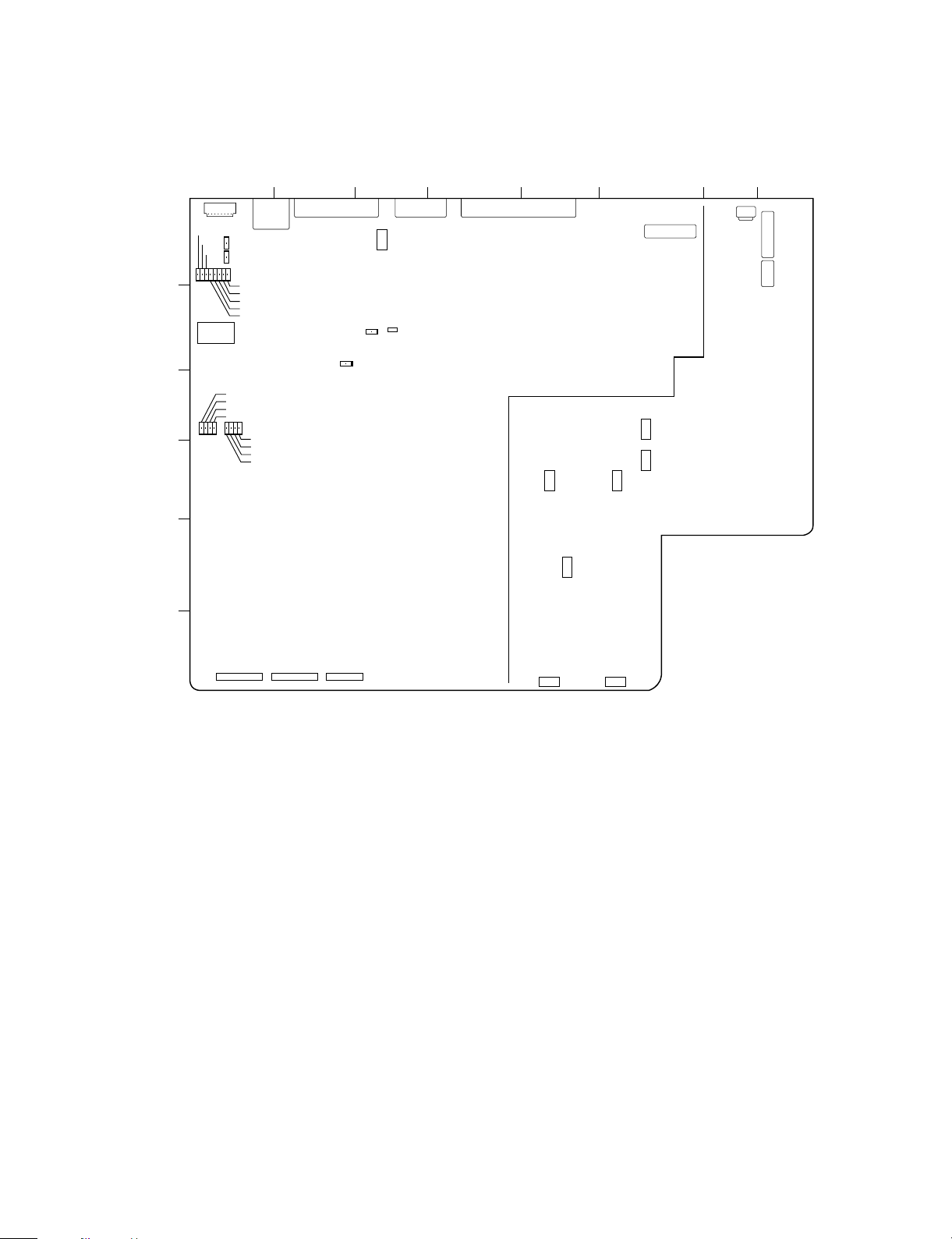
1-6. Switch setting and LED function
SSP-11 board (A side)
ABCDE FG
H
CN702
D303
D304
1
2
3
4
5
6
D316
D305
D317
D310
D309
D308
D307
D306
S302
D608
D607
D606
D605
D601
D602
D603
D604
CN405 CN406 CN309
CN308
CN305
D302
D301
CN306 CN307
S801*1
S301
RV203
1
S202
S51
RV202
1
RV201*1
1
S201 S101
S102
RV206*1
1
RV102
RV103
1
RV106*1
1
1
RV101*1
1
CN51
S203*1
S103*1
CN1
CN3
CN2
*1 :Applicable board number suffix ; -12 and higher
LED indicators
D301 (C2) (red) : CPU initialization indicator
Turns on when reset, and turns off
when initialization process is completed.
D302 (B2) (yellow) : EEPROM access indicator
Turns on during data read/write of
EEPROM (IC308).
D303 (A1) (red) : Backup memory data initialization
indicator
Turns on when backup memory
(IC309, IC310) is initilized (cleared).
D304 (A1) (green) : Normal operation indicator
Turns on when when the main CPU
(IC304) operates normally.
D305 (A1) (yellow) : Mute indicator
Turns on when the playback audio
signal is muted (in such mode as STOP).
D306 (A1) (yellow) : DSP output indicator
Turns on when the monitor sound is
(any of the following) DSP (IC604)
outputs.
. The SYNC REC lamp on the front
panel turns on. (sync record mode)
. Memory jog, memory rehearsal
and memory start play
D307 (A1) (yellow): RMW mode indicator
Turns on when the leading head is
playing back and the trailing head is
recording (any of the followings).
. The SYNC REC lamp on the front
panel turns on. (sync record mode)
. When playing back the wide track
pitch tape.
. When the leading head playback
mode is selected by the error rate
selection (service menu “rAtE
SEL”).
D308 (A1) (green) : 9-pin CPU interface normal operation
indicator
Turns on when communication
between the 9-pin CPU (IC318) and
the main CPU (IC304) is established.
PCM-7040
1-5(E)

D309 (A1) (red) : 9-pin data reception (9-pin CPU →
main CPU) indicator
Turns on while the main CPU is
receiving data from the 9-pin CPU.
D310 (A1) (green) : 9-pin data send (9-pin CPU ← main
CPU) indicator
Turns on while the main CPU is
sending data to the 9-pin CPU.
D316 (A1) (red) : 9-pin data reception (SCU → 9-pin
CPU) indicator
Turns on while the 9-pin CPU is
receiving data from the SCU (Serial
Control Unit, IC306).
D317 (A1) (green) : 9-pin data send (SCU ← 9-pin CPU)
indicator
Turns on while the 9-pin CPU is
sending data to the SCU.
D601 (A3) (red) : Recorder (playback sound) sound
memory write indicator
Turns on while writing data into the
recorder sound memory.
D602 (A3) (yellow) : Recorder (playback sound) sound
memory read indicator
Turns on while reading data from
the recorder sound memory.
D603 (A3) (green) : Recorder (playback sound) sound
memory IN-point trigger indicator
Turns on when cross-fade is applied
to the recorder sound memory data
at IN-point.
D604 (A3) (green) : Recorder (playback sound) sound
memory OUT-point trigger indicator
Turns on when cross-fade is applied
to the recorder sound memory data
at OUT-point.
D605 (A3) (red) : Player (input sound) sound memory
write indicator
Turns on while writing data into the
player sound memory.
D606 (A3) (yellow) : Player (input sound) sound memory
read indicator
Turns on while reading data from
the player sound memory.
D607 (A3) (green) : Player (input sound) sound memory
IN-point trigger indicator
Turns on when cross-fade is applied
to the player sound memory data at
IN-point.
D608 (A3) (green) : Player (input sound) sound memory
OUT-point trigger indicator
1-6(E)
Switches
S301 (C2) : RESET switch
CPU (IC304) reset switch
S302 (A2) : Mode setting
S302-1, 2: Destination setting
S302-1 S302-2 Destination setting
OFF OFF For UC
ON OFF For J
OFF ON For CE
ON ON For UC
S302-3, 4: Device type setting for 9 PIN
S302-3 S302-4 Device type setting
for 9PIN
OFF OFF PCM-7030
(Factory setting)
ON OFF PCM-7050
OFF ON PCM-7040
ON ON PCM-7040
S302-5 to -7 : Reserved
S302-8 : Backup memory initialization
setting
S302-8: Backup memory initialization setting
OFF Not initialized when the main power is
turned on.(Factory setting)
ON Initialized when the main power is turned
on. “-ALL cLEAr-” appears on the display.
In the cases as described below, set the
destination using S302-1 and -2, then
perform initialization.
1. When the SSP-11 board is replaced.
2. When IC309 or IC310 (RAM) on the
SSP-11 board is replaced.
When any switch of S302-5 to -7 is set to on, the
ALARM indicator on the front panel flashes, and
“cAution 1-50” is triggered.
Factory setting
S302-1, -2 ; Items 1 and 2 are set in accordance
with destination.
S302-3 to -8; off
PCM-7040
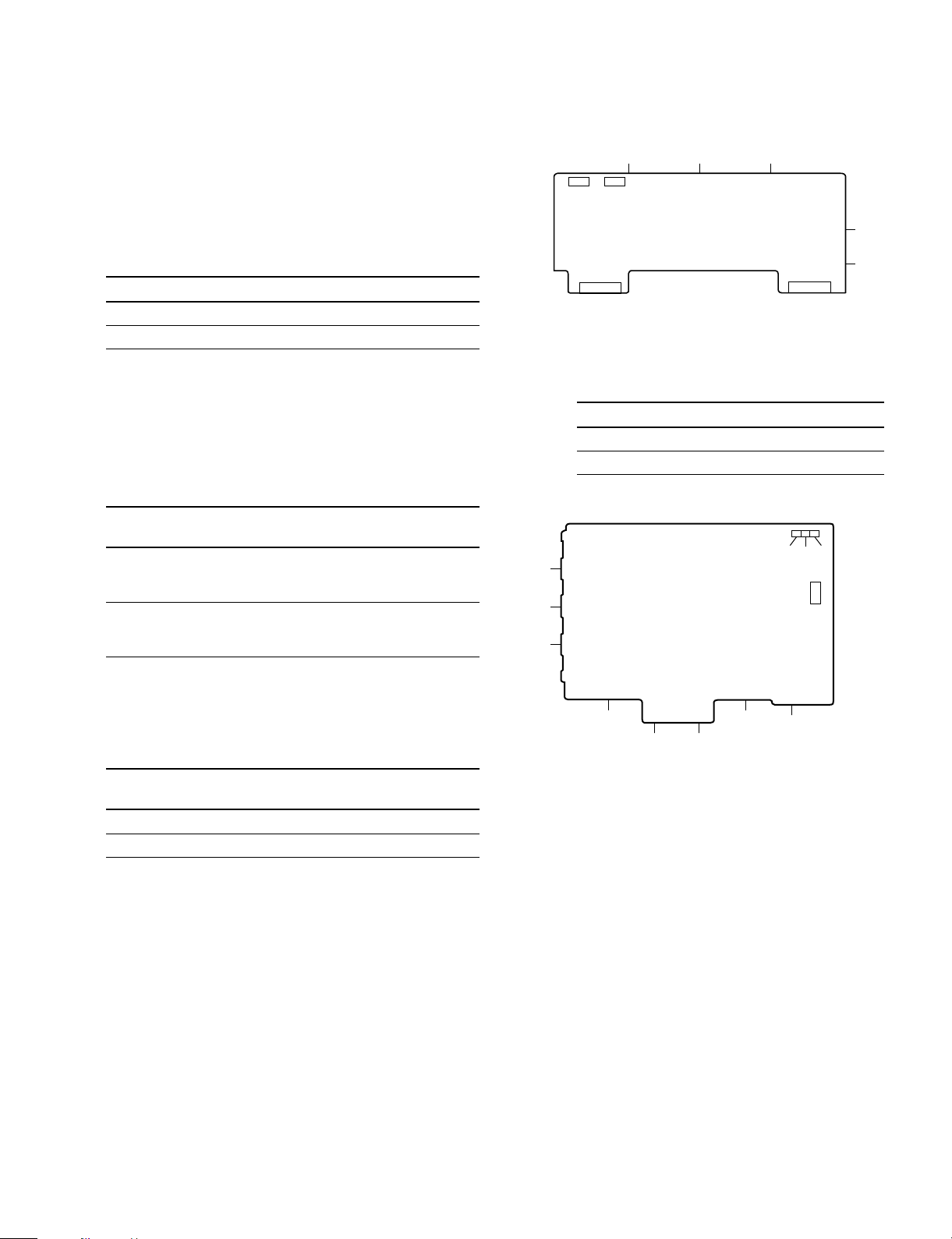
S801(C1):Used during designing
Factory setting ; LO side position
S51 (E5) : AD/DA signal path switch
Switch for AD/DA digital audio signal changing over
S51 Signal path setting
NORMAL Normal signal path(Factory setting)
TEST AD converter output is input to the DA converter
S101 (F6) : Input reference signal level (CH-1) switch
S201 (E6) : Input reference signal level (CH-2) switch
S102 (F4) : Output reference signal level (CH-1) switch
S202 (E4) : Output reference signal level (CH-2) switch
Reference signal level (+4 dBs/_20 dBs)
changing switches
S101, S102, Reference signal level setting
S201, S202
+4 dBs The +4 dBs input/output signal will be
displayed as _20 dB on the level meter
(FL display).(factory setting)
_20 dBs The _20 dBs input/output signal will be
displayed as _20 dB on the level meter
(FL display).
(0 dBs = 0.775 Vrms)
S103 (F4) : MONITOR output reference level (CH-1) switch
S203 (F4) : MONITOR output reference level (CH-2) switch
Reference output level changing switches for
MONITOR output connectors (CH-1, CH-2)
S103, S203 Reference output level setting of
MONITOR output connectors (CH-1, CH-2)
+10 _10 dBs(factory setting)
0 _20 dBs
CP-268 board (A-side)
Switches
ABCD
S11 S21
CN52 CN501
S11 (A1) :
Analog audio (CH-1) input impedance setting switch
Set the CH-1 input impedance.
S21 (A1) :
Analog audio (CH-2) input impedance setting switch
Set the CH-2 input impedance.
S11, 21 Input impedance setting
OFF 10 kZ
ON 600 Z (Factory setting)
SV-147A board (B-side)
A
B
C
D
21
3
4
D3S1D2
D1
56
Switch
S1 (S1-1 to S1-4) ; Adjustment Mode Setting Switch
(For details, refer to “Section 4.
Replacement and Adjustment of
Mechanism Deck”)
1
2
3
When reference level has been changed, adjust the following volumes.
RV102 (F6) : Adjustment for input level (CH1)
RV202 (E6) : Adjustment for input level (CH2)
RV103 (F4) : Adjustment for output level (CH1)
RV203 (E4) : Adjustment for output level (CH2)
RV106(F4) : Adjustment for output linearity (CH-1)
RV206(F4) : Adjustment for output linearity (CH-2)
PCM-7040
Factory setting
S1-1 to S1-4 ; All OFF
(Setting for normal operations)
LED indicators
D1 ; CPU Operation Indicator
Blinking (Approx.every 1 sec.)
: When operating normally.
Blinking quickly (Approx.every 0.5 sec.)
: When an error is detected.
Lit or off : When not operating
D2 ; Adjusting Mode Indicator
Lit : When adjustment mode is ON.
Off : When adjustment mode is OFF.
D3 ; Servo Lock Indicator
Lit : Locked
Off : Unlocked
1-7(E)

1-7. ISR (Interactive Status Reporting)
The PCM-7040 corresponds to a ISR (Interactive Status Reporing) function.
Using this function, the status of the PCM-7040 or the contents of a generated error can be intensively monitored and
managed on the monitor screen of a personal computer. The data displayed on the monitor screen can be stored or printed as
a file.
The major functions of the PCM-7040 are as follows.
Management functions
. Identification information
Manufacture : SONY
Model : PCM-7040
Device ID : Identification number or identification name within 50 alphanumeric characters.
Serial number : Serial number which is set from the PCM-7040 (service menu).
VM type : 02 (VTR)
Destination : Destination UC, J, CE
ROM : ROM information for main CPU, servo CPU and display CPU (Board name, ROM name, version, board
address)
. Hour meter information
Integrating meter for Operation, Drum Running, Tape Running, Threading Counter
. Upload and download of setup menu data (global setting)
Monitor function
. Error/caution message
Indication of the error or caution (warning) number and its meaning. Or indication of error history.
. Signal processing error (Channel Condition) message
Indication of signal processing error. Or indication of error history.
Level:
0: Good
1: Correction of certain amount of error or more
2: Interpolation
4: Mute
. Operation statas
Indication for tape path mode
TAPE UNTHREAD, STOP, STANDBY OFF, PLAY, PLAY LOCK, REC, REC LOCK, EDIT, EDIT LOCK, F.FWD,
REW, SHUTTLE STILL, SHUTTLE FWD, SHUTTLE REV, JOG STILL, JOG FWD, JOG REV, VAR STILL,
VAR FWD, VAR REV, PREROLL, PREVIEW, AUTO EDIT, CHASE
. Test
Main CPU test, sound memory test
Control function
. Remote control
EJECT, STANDBY ON/OFF, STOP, PLAY, REC, F.FWD, REW, CUEUP(TC LOCATE)
1-8(E)
PCM-7040
Section 5
Electrical Alignment
This section describes the following electrical adjustment
when SSP-11 board is repaired or maintained.
SSP-11 board adjustment items
5-2. Signal processing block adjustment
5-2-1. Master clock adjustment
5-2-2. Timer clock adjustment
5-2-3. RF PLL adjustment
5-3. AD/DA block adjustment
5-3-1. AD conversion level adjustment
5-3-2. DA conversion level adjustment
5-3-3. C.M.R.R adjustment
5-3-4. Output balance adjustment
5-4. Time code output level adjustment
5-1. Preparation
5-1-1. Equipment
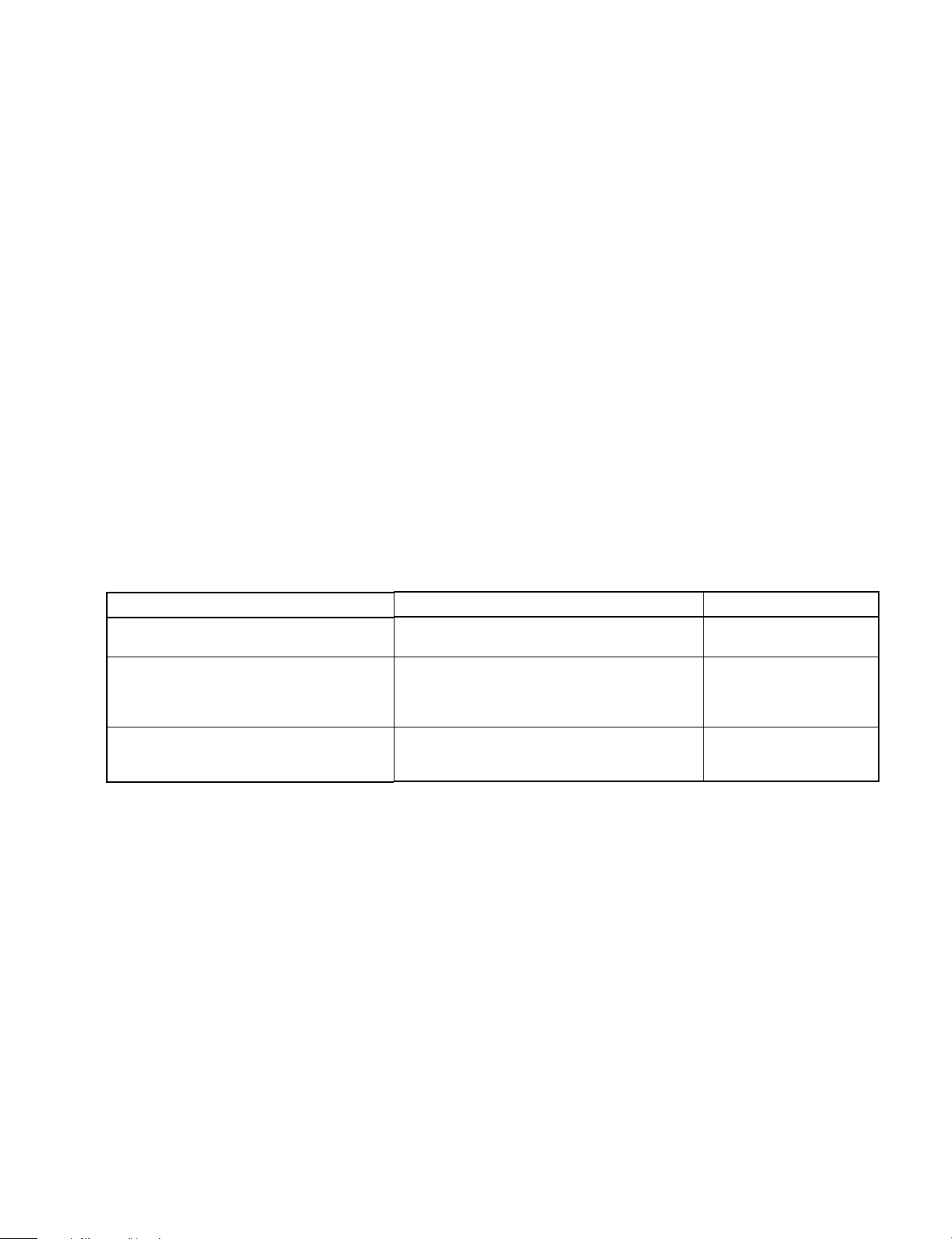
Equipment
Oscilloscope
Audio analyzer
Frequency counter
Specification
Frequency:DC to 150 MHz
Dual trace or more (Add mode)
. AF Oscillator
Range:10 to 100 kHz
Level:_70 to +24 dBm
. Level meter
Effective digits:8 digits or more
Model name
TEKTRONIX 2445A
or equivalent
TEKTRONIX SG505 (OP2),
AA501
or equivalent
ADVAN TEST TR5822,
HEWLETT PACKARD 5315A
or equivalent
PCM-7040
5-1(E)
5-1-2. Switch and Control Initial Setting
5-2. Signal Processing Block Adjustment
Front panel
Switches
REMOTE (9P)/LOCAL ; LOCAL
SYNC EXT/INT/VIDEO ; INT
AUDIO INPUT ANALOG/DIGITAL ; ANALOG
SAMPLING FREQ 44.1 kHz/48 kHz ; 48 kHz
Controls
ANALOG CH-1 input level; Center click position
ANALOG CH-2 input level; Center click position
SSP-11 board
AD/DA block
S51 switch; NORMAL
S101 switch; +4
S201 switch; +4
S102 switch; +4
S202 switch; +4
S103* switch; +0
S203* switch; +0
CPU-268 board
S11 switch; ON (600Z)
S21 switch; ON (600Z)
* Applicable board No. suffix ; -12 and higher
To perform the adjustments, first remove the top panel.
5-2-1. Master Clock Adjustment
This section describes the oscillation frequency adjustments of X’tal which generates the Fs system clock of
master clock block.
Perform the adjustment/checking when SSP-11 board and
master clock block components are replaced.
Equipment required
Frequency counter
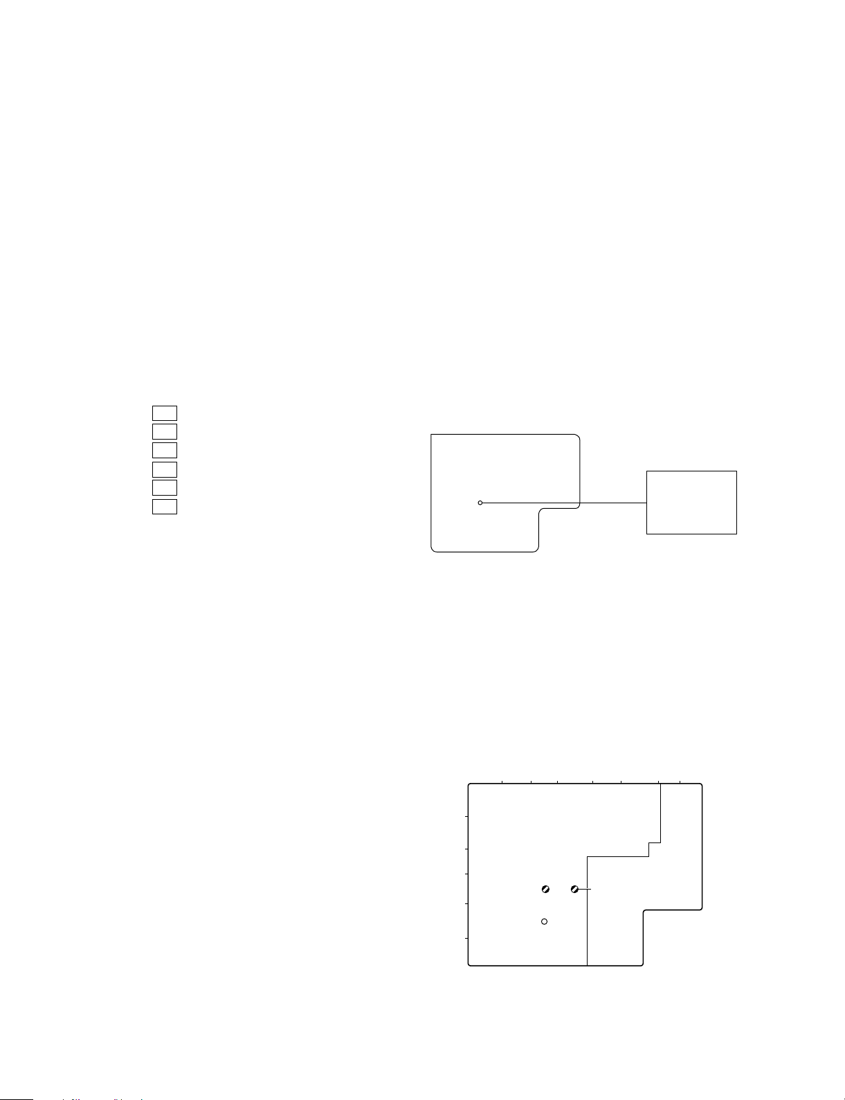
Connection
Frequency counter
TP50
SSP-11 board (A side)
Switch and control setting
Same as “5-1-2. Switch and Control Initial Setting” except
the followings:
Front panel
REMOTE (9P)/LOCAL switch ; LOCAL
SYNC EXT/INT/VIDEO switch ; INT
SAMPLING FREQ 44.1 kHz/48 kHz switch ; 48 kHz
5-2(E)
Adjustment Location
A2BC D E F GH
1
3
4
5
6
*1 Applicable board No. suffix ; -11
*2 Applicable board No. suffix ; -12 and higher
*1
CT401 (C4)
*2
or X403 (C4)
TP50 (C5)
*1
CT402 (D4)
*2
or X404 (D4)
SSP-11 board (A-side)
PCM-7040
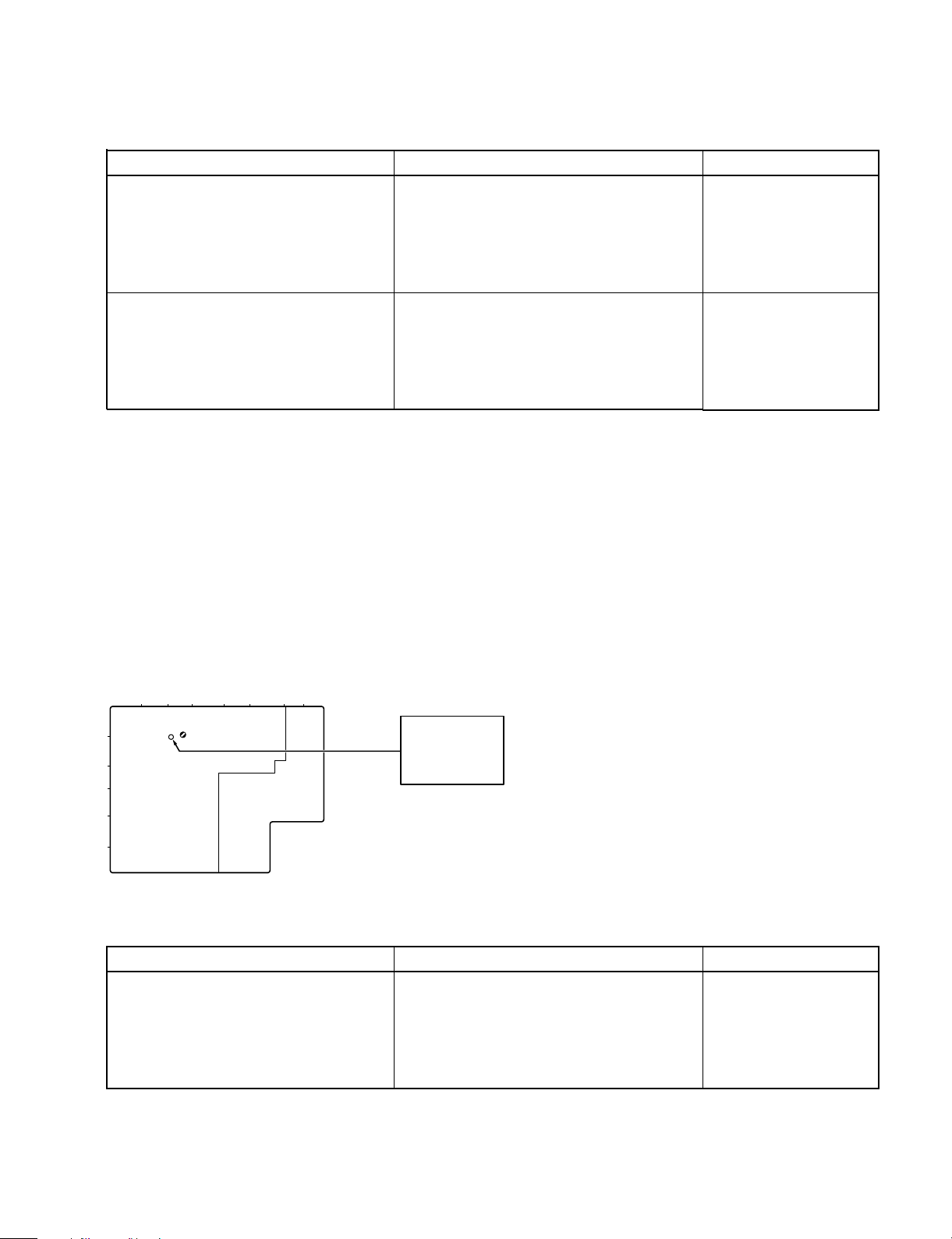
Adjustment procedure
Adjustment condition
Step 1
. Disconnect the connecting cables of rear panel.
. Connect the frequency counter to the TP50
(C5)/SSP-11 board.
. Check that the frequency at TP50 (C5) satisfies the
following specification (47999.76 to 48000.24 Hz).
If the specification are not satisfied, adjust the
*1
CT401
(C4)/X403*2 (C4).
. SAMPLING FREQ. switch(Front panel)
: 48 kHz
Specification (frequency at TP50)
Fs (48 kHz) = 48000.00 ±0.24 Hz
Step 2
The settings remain in the same as step 1
except the following.
. SAMPLING FREQ. switch(front panel)
. Check that the frequency at TP50 (C5) satisfies the
following specification (44099.78 to 44100.22 Hz).
If the specifications are not satisfied, adjust the
CT402*1 (D4)/X404*2 (D4).
: 44.1 kHz
Specification (frequency at TP50)
Fs (44.1 kHz) = 44100.00 ±0.22 Hz
5-2-2. Timer Clock Adjustment
Perform the adjustment/checking when SSP-11 board and
time clock block components (X304, CT301 and peripheral components) are replaced.
Equipment required
Frequency counter
Specification
Adjustment (SSP-11 board)
*1 Board No. suffix: -11
1CT401 (C4)
*2 Board No. suffix:
-12 and higher
1X401 (C4)
*1 Board No. suffix: -11
1CT402(D4)
*2 Board No. suffix:
-12 and higher
1X404 (D4)
Switch and control setting
This has no switches and controls that need to be set during
adjustment.
Connection/Adjustment Location
A2BC D E FGH
1
TP36 (C2)
3
4
5
6
CT301 (C2)
SSP-11 board (A-side)
Adjustment procedure
Adjustment condition
. Connect the frequency counter to the TP36
(C2) SSP-11 board.
Frequency counter
Specification
. Check that the frequency at TP36 (C2) satisfies the
following specification (2047.99 to 2048.01 Hz).
If the specifications are not satisfied, adjust the
CT301 (C2).
Specification
Frequency at TP36 = 2048.00 ±0.01 Hz
Adjustment (SSP-1 board)
1CT301 (C2)
PCM-7040
5-3(E)
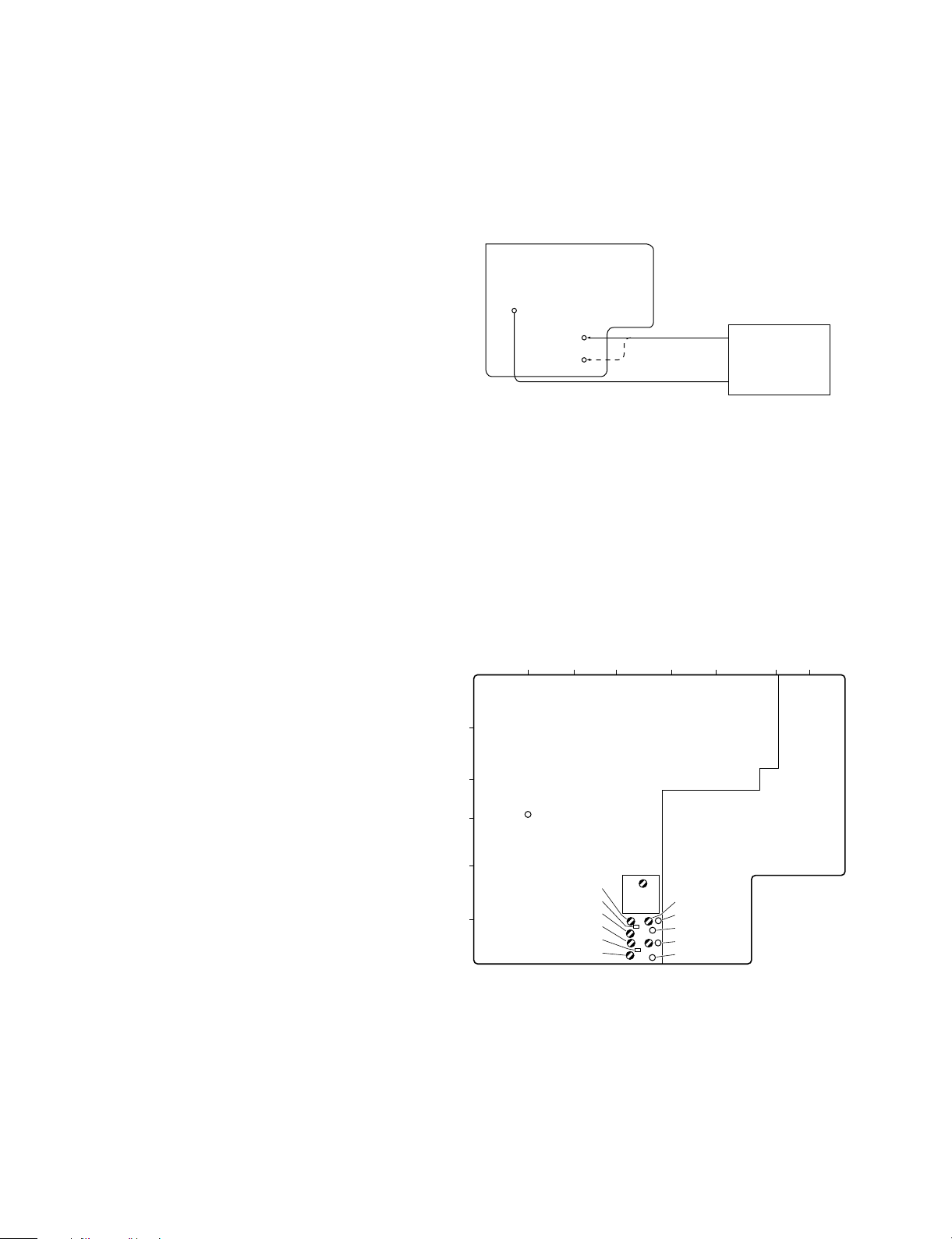
5-2-3. RF PLL Adjustment
The RF PLL block generates the clock for extracking the
playback data from the head. In correspondence to the
head/RF amplifier characteristics, adjust the RF PLL block
to obtain the best error rate.
Perform this adjustment when replacing SSP-11 board and
RF PLL block components, and replacing the mechanism
assembly, drum assembly and RF assembly.
Preparation
. Disconnect the connection plugs (COP401 and COP402)
from the connection pins (COR401 and COR402) (D6)
on the SSP-11 board. (See “Adjustment Location”.)
The connection plugs (COP401 and COP402) are to be
reinserted after the RF PLL adjustment.
Equipment required
Oscilloscope
Pre-recorded music DAT tape (Fs = 48 kHz)
Connection
TP512 (A3)
TP53 (D6)
TP55 (D6)
SSP-11 board (A side)
Oscilloscope
CH 1
CH 2
CH 1; 1 V/div
CH 2; 5 V/div
10 ms/div
Switch and Control setting
Same as “5-1-2. Switch and Control Initial Setting” except
the followings:
Front panel
REMOTE (9P)/LOCAL switch ; LOCAL
SYNC EXT/INT/VIDEO switch ; INT
SAMPLING FREQ 44.1 kHz/48 kHz switch ; 48 kHz
Adjustment Location
A
1
2
3
4
5
6
BC D E FGH
TP512 (A3)
RV401 (C6)
COR402 (D6)
LV402 (C6)
RV403 (C6)
COR401 (D6)
LV403 (C6)
LV401
(D5)
RV402 (D6)
TP54 (D6)
TP53 (D6)
TP56 (D6)
TP55 (D6)
SSP-11 board (A-side)
5-4(E)
PCM-7040
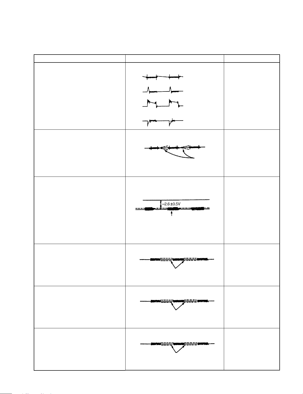
1. Leading head RF PLL Adjustment
Adjustment Condition
Step 1
. Connect the oscilloscope as follows:
Oscilloscope SSP-11 board
CH1 → TP53 (D6)
CH2 → TP512 (A3)
(TRIGGER)
. Insert the pre-recorded music cassette tape
(Fs = 48 kHz) and playback the tape. (PLAY
mode)
Step 2
Same as step 1.
Step 3
Same as step 1.
Step 4
. Insert the pre-recorded music cassette tape
(Fs = 48 kHz) and set CUE FWD (X16 speed).
. The connectings remain the same as step 1.
Specification
TP53 (D6) output waveform
OK
NG
NG
NG
TP53 (D6) output waveform
TP53 (D6) output waveform
Amplitude’s center voltage where is RF.
TP53 (D6) output waveform
TRIG: TP512 (A3)
This portion
is to be flat.
TRIG: TP512 (A3)
TRIG: TP512 (A3)
Adjustment (SSP-11 board)
1RV402 (D6)
If the waveform is no good,
turn 1RV401 slightly and then
readjust 1RV402.
1RV401 (C6)
1LV402 (C6)
Note: After being turned
clockwise all the way,
adjust 1LV402 so that
it can be loosened
within one full turn. If it
is too tight, the core
may be damaged. And
if it is too loose, the
core may come off.
1RV402 (D6)
Step 5
. Insert the pre-recorded music cassette tape
(Fs = 48 kHz) and set CUE REV (X16 speed).
. The connectings remain the same as step 1.
Step 6
. Insert the pre-recorded music cassette tape
(Fs = 48 kHz) and set CUE FWD and CUE
REV (X3 speed). Repeatedly two or three
times.
. The connectings remain the same as step 1.
PCM-7040
This portion is to be flat.
TRIG: TP512 (A3)
TP53 (D6) output waveform
This portion is to be flat.
TRIG: TP512 (A3)
TP53 (D6) output waveform
This portion is to be flat while the tape is running.
TRIG: TP512 (A3)
1RV402 (D6)
5-5(E)
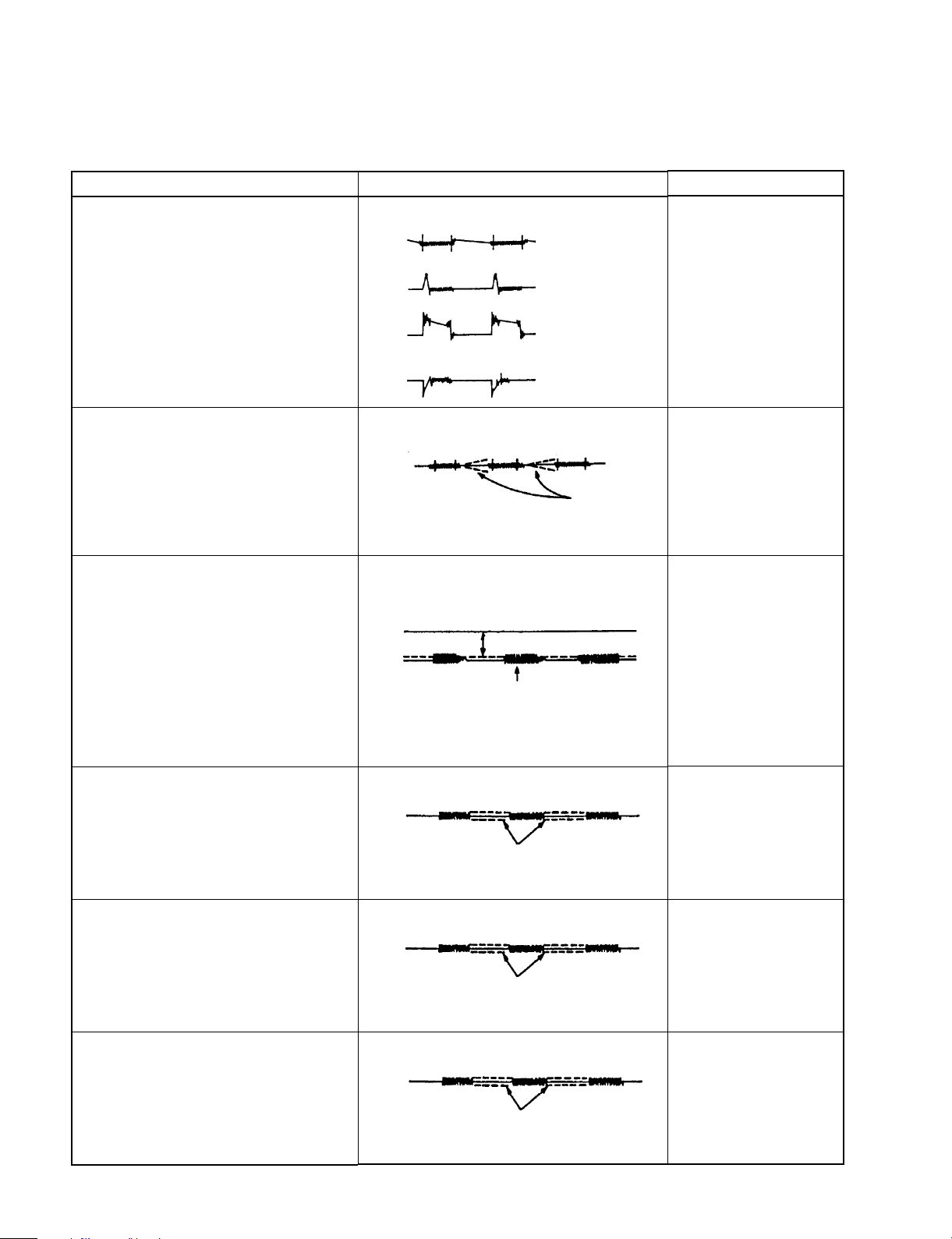
2. Trailing head RF PLL Adjustment
Adjustment Condition
Step 1
. Connect the oscilloscope as follows:
Oscilloscope SSP-11 board
CH1 → TP55 (D6)
CH2 → TP512 (A3)
(TRIGGER)
. Insert the pre-recorded music cassette tape
(Fs = 48 kHz) and playback the tape. (PLAY
mode)
Step 2
Same as step 1.
Step 3
Same as step 1.
Step 4
. Insert the pre-recorded music cassette tape
(Fs = 48 kHz) and set CUE FWD (X16 speed).
. The connectings remain the same as step 1.
Specification
TP55 (D6) output waveform
OK
NG
NG
NG
TP55 (D6) output waveform
TP55 (D6) output waveform
_2.6 ± 0.5V
Amplitude’s center voltage where is RF.
TP55 (D6) output waveform
TRIG: TP512 (A3)
This portion
is to be flat.
TRIG: TP512 (A3)
TRIG: TP512 (A3)
Adjustment (SSP-11 board)
1RV404 (D6)
If the waveform is no good,
turn 1RV403 slightly and
then readjust 1RV404.
1RV403 (C6)
1LV403 (C6)
Note: After being turned
clockwise all the way,
adjust 1LV403 so that
it can be loosened
within one full turn. If it
is too tight, the core
may be damaged. And
if it is too loose, the
core may come off.
1RV404 (D6)
Step 5
. Insert the pre-recorded music cassette tape
(Fs = 48 kHz) and set CUE REV (X16 speed).
. The connectings remain the same as step 1.
Step 6
. Insert the pre-recorded music cassette tape
(Fs = 48 kHz) and set CUE FWD and CUE
REV (X3 speed). Repeatedly two or three
times.
. The connectings remain the same as step 1.
5-6(E)
This portion is to be flat.
TRIG: TP512 (A3)
TP55 (D6) output waveform
This portion is to be flat.
TRIG: TP512 (A3)
TP55 (D6) output waveform
This portion is to be flat while the tape is running.
TRIG: TP512 (A3)
1RV404 (D6)
PCM-7040
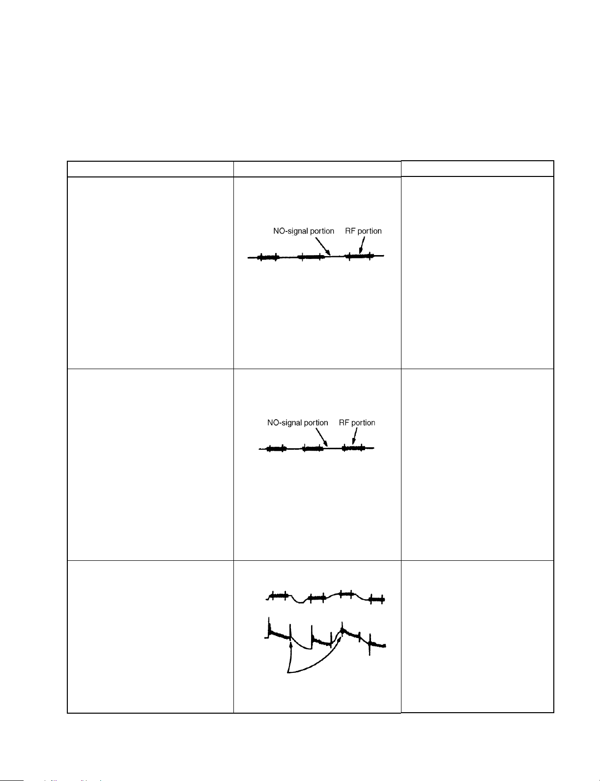
3. RF PLL Fine Adjustment
Preparation:
Before performing the adjustment, turn off the POWER switch and reinsert the connection plugs (COP401 and COP402)
into the connection pins (COR401 and COR402) on the SSP-11 board.
Then turn on the POWER switch and perform the adjustment.
Adjustment Condition
Step 1
. Connect the oscilloscope as follows:
Oscilloscope SSP-11 board
CH1 → TP55(D6)
CH2 → TP512(A3)
(TRIGGER)
. Insert the pre-recorded music cassette
tape (Fs = 48 kHz) and playback the tape.
(PLAY mode)
Step 2
. Connect the oscilloscope as follows:
Oscilloscope SSP-11 board
CH1 → TP53(D6)
CH2 → TP512(A3)
(TRIGGER)
. Insert the pre-recorded music cassette
tape (Fs = 48 kHz) and playback the tape.
(PLAY mode)
Specification
TP55 (D6) output waveform
TP53 (D6) output waveform
TRIG: TP512 (A3)
Adjustment (SSP-11 board)
1LV401 (D5)
Adjust 1LV401 so that the center of the
RF portion and no signal portion
becomes flat. If the center cannot be
flattened, redo the adjustments from
steps 3 to 6 for “2. Trailing head RF PLL
adjustment”.
Before making the re-adjustment, shift
the center voltage within the adjustment
standard range stated in step 3 of “2.
Trailing head RF PLL adjustment”.
Note: After being turned clockwise all
the way, adjust 1LV401 so that it
can be loosened within one full
turn. If it is too tight, the core may
be damaged. And if it too loose,
the core may come off.
1LV402 (C6)
Adjust 1LV402 so that the center of the
RF portion and no signal portion
becomes flat. If the center cannot be
flattened, redo the adjustments from
steps 3 to 6 for “1. Leading head RF PLL
adjustment”.
Before making the re-adjustment, shift
the center voltage within the adjustment
standard range stated in step 3 of “1.
Leading head RF PLL adjustment”.
Step 3
. Connect the oscilloscope as follows:
Oscilloscope SSP-11 board
CH1 → TP53(D6), TP55(D6)
CH2 → TP512(A3)
(TRIGGER)
. Insert the pre-recorded music cassette
tape (Fs = 48 kHz) and set the FF and
REW modes.
PCM-7040
TRIG: TP512 (A3)
TP53 (D6) and TP55 (D6) output waveform
OK
NG
As the voltage is high, the waveform swings
to plus.
TRIG: TP512 (A3)
Note: After being turned clockwise all
the way, adjust 1LV402 so that it
can be loosened within one full
turn. If it is too tight, the core may
be damaged. And if it too loose,
the core may come off.
5-7(E)
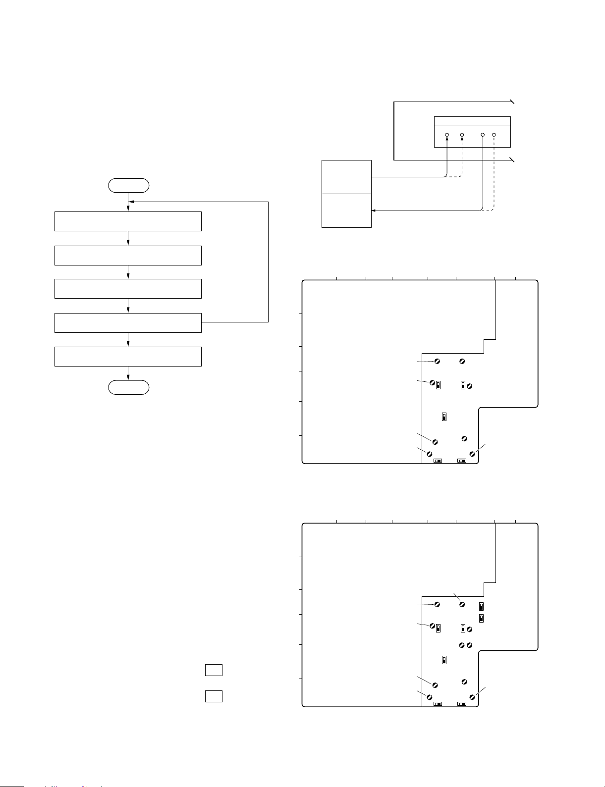
5-3. AD/DA Block Adjustment
To perform the adjustments, first remove the top panel.
Perform the adjustments according to the following
adjustment procedure.
AD/DA Block adjustment procedure
START
5-3-1. AD conversion level adjustment
Connection
Audio analyzer
Oscillator
Level meter
Rear panel
ANALOG
INPUT
CH1CH2 CH1 CH2
OUTPUT
5-3-2. DA conversion level adjustment
5-3-3. C.M.R.R Adjustment
AD conversion level checking : OK
YES
5-3-4. Output balance adjustment
END
NO
Equipment required
Audio analyzer
Oscilloscope
Switch and control setting
Same as “5-1-2. Switch and Control Initial Setting” except
the followings:
Front panel
SAMPLING FREQ 44.1 kHz/48 kHz switch ; 48 kHz
AUDIO INPUT ANALOG/DIGITAL switch ; ANALOG
ANALOG CH-1 input level control
; click center position
ANALOG CH-2 input level control
; click center position
INPUT MONITOR key
; ON (LED lighting)
SSP-11 board (AD/DA block)
S101, S102, S201, S202 switches ; +4
S151 switch ; NORMAL
S103*, S203* switches ; +0
* Applicable board No. suffix ; -12 and higher
CP-268 board
S11, S21 switch ; ON (600Z)
5-8(E)
Adjustment Location
A
1
2
3
4
5
6
A
1
2
3
4
5
6
BC D E F GH
RV205 (E3)
RV203 (E4)
RV202 (E6)
RV201 (E6)
BC D E F GH
RV205 (E3)
RV203 (E4)
RV202 (E6)
RV201 (E6)
RV105 (F3)
S202 S102
S151
RV105 (F3)
S202 S102
S151
SSP-11 board (A-side)
Board No. 1-633-709-12 and higher
RV103 (F4)
RV102
(F5)
RV101 (F6)
S101S201
SSP-11 board (A-side)
Board No. 1-633-709-11
S203
S103
RV103 (F4)
RV106 (F4)RV206 (F4)
RV102
(F5)
RV101 (F6)
S101S201
PCM-7040

5-3-1. AD Conversion Level Adjustment
Perform the AD block adjustments on the SSP-11 board,
perform the adjustment first.
Preparation
Before performing the adjustment, set the FL tube display
on the front panel as follows. For setting, refer to the
operation manual.
FL tube display (front panel)
Au-rEF (input signal level’s digital indication mode)
EMPH OFF (emphasis OFF mode)
Adjustment condition
Step 1
. Input a 1 kHz, +4 dBs (0 dBs = 0.775 Vrms)
signal to the ANALOG IN CH-1 connector from
the audio analyzer (AF oscillator).
Step 2
. Input a 1 kHz, +4 dBs (0 dBs = 0.775 Vrms)
signal to the ANALOG IN CH-2 connector from
the audio analyzer (AF oscillator).
Value of the Au-rEF CH1 (left side) on the FL tube
display
Value of the Au-rEF CH2 (right side) on the FL tube
display
5-3-2. DA Conversion Level Adjustment
Perform the DA block adjustments on the SSP-11 board,
perform this adjustment after completing “5-3-1. AD
conversion level adjustment”.
1. Adjustment for board No. suffix -11
Adjustment condition
Step 1
ANALOG OUTPUT CH-1 output level:
_20.0 dB
_20.0 dB
Specification
Specification
Adjustment (SSP-11 board)
1RV102 (F5)
1RV202 (E6)
Adjustment (SSP-11 board)
1RV103 (F4)
. Input a 1 kHz, +4 dBs (0 dBs = 0.775 Vrms)
signal to the ANALOG IN CH-1 connector from
the audio analyzer (AF oscillator).
. Connect the audio analyzer (level meter) to the
ANALOG OUTPUT CH-1 connctor.
Step 2
. Input a 1 kHz, +4 dBs (0 dBs = 0.775 Vrms)
signal to the ANALOG IN CH-2 connector from
the audio analyzer (AF oscillator).
. Connect the audio analyzer (level meter) to the
ANALOG OUTPUT CH-2 connctor.
PCM-7040
+4.0 dBs ±0.1 dB
ANALOG OUTPUT CH-2 output level:
+4.0 dBs ±0.1 dB
1RV203 (E4)
5-9(E)
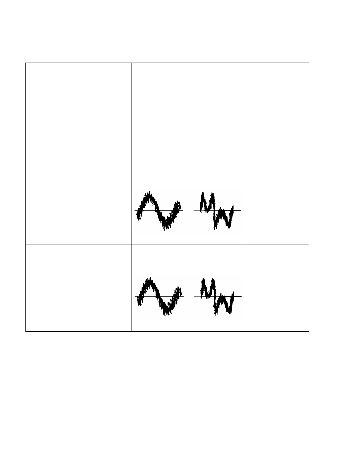
2. Adjustment for board No. suffix -12 and higher
Adjustment condition
Step 1
. Input a 1 kHz, +4 dBs (0 dBs = 0.775 Vrms)
signal to the ANALOG IN CH-1 connector from
the audio analyzer (AF oscillator).
. Connect the audio analyzer (level meter) to the
ANALOG OUTPUT CH-1 connctor.
Step 2
. Input a 1 kHz, +4 dBs (0 dBs = 0.775 Vrms)
signal to the ANALOG IN CH-2 connector from
the audio analyzer (AF oscillator).
. Connect the audio analyzer (level meter) to the
ANALOG OUTPUT CH-2 connctor.
Step 3
. Input a 1 kHz, _60 dBs (0 dBs = 0.775 Vrms)
signal to the ANALOG IN CH-1 connector from
the audio analyzer (AF oscillator).
. Connect the audio analyzer (level meter) to the
ANALOG OUTPUT CH-1 connctor.
. Connect the oscilloscope to the monitor output
of audio analyzer.
Specification
ANALOG OUTPUT CH-1 output level:
+4.0 dBs ±0.1 dB
ANALOG OUTPUT CH-2 output level:
+4.0 dBs ±0.1 dB
Satisfy 1, 2 below both at the same time.
1 Output level of CH-1:
Between _60.0 to _60.5 dBs
2 Oscilloscope waveform : sine wave
Adjustment (SSP-11 board)
1RV103 (F4)
1RV203 (E4)
1RV106 (F4)
Step 4
. Input a 1 kHz, _60 dBs (0 dBs = 0.775 Vrms)
signal to the ANALOG IN CH-2 connector from
the audio analyzer (AF oscillator).
. Connect the audio analyzer (level meter) to the
ANALOG OUTPUT CH-2 connctor.
. Connect the oscilloscope to the monitor output
of audio analyzer.
OK (sine wave) NG
Satisfy 1, 2 below both at the same time.
1 Output level of CH-2:
Between _60.0 to _60.5 dBs
2 Oscilloscope waveform : sine wave
OK (sine wave) NG
1RV206 (F4)
5-10(E)
PCM-7040

5-3-3. C. M. R. R. Adjustment
FL tube display (front panel) setting
Au-rEF (Input signal level's digital indication)
Adjustment procedure
Adjustment condition
Step 1
. Input the in-phase signal of 1 kHz, +4 dBs (0
dBs = 0.775 Vrms) to the ANALOG IN CH-1
connector, from an audio analyzer (AF
oscillator).
Connection of the input signal must be made
between hot (pin-2) and GND (pin-1), and
between cold (pin-3) and GND (pin-1) of the
CH-1 connector, in parallel.
. Connect an audio analyzer (level meter) to the
ANALOG OUTPUT CH-1 connector.
Step 2
. Input the in-phase signal of 1 kHz, +4 dBs (0
dBs = 0.775 Vrms) to the ANALOG IN CH-2
connector, from an audio analyzer (AF
oscillator).
Connection of the input signal must be made
between hot (pin-2) and GND (pin-1), and
between cold (pin-3) and GND (pin-1) of the
CH-2 connector, in parallel.
. Connect an audio analyzer (level meter) to the
ANALOG OUTPUT CH-2 connector.
Specification
ANALOG OUTPUT CH-1 output level:
_56 dBs or less
. Confirm at this time that the numeric value
appearing on Au-rEF (left side) of the FL tube
display satisfies the specification indicated in
section “5-3-1. AD Conversion Level Adjustment”.
When the specification is not satisfied, perform
step 1 of section “5-3-1. AD Conversion Level
Adjustment” again until the specification is
satisfied.
ANALOG OUTPUT CH-2 output level:
_56 dBs or less
. Confirm at this time that the numeric value
appearing on Au-rEF (left side) of the FL tube
display satisfies the specification indicated in
section “5-3-1. AD Conversion Level Adjustment”.
When the specification is not satisfied, perform
step 2 of section “5-3-1. AD Conversion Level
Adjustment” again until the specification is
satisfied.
Adjustment (SSP-11 board)
1RV101 (F6)
1RV201 (E6)
PCM-7040
5-11(E)
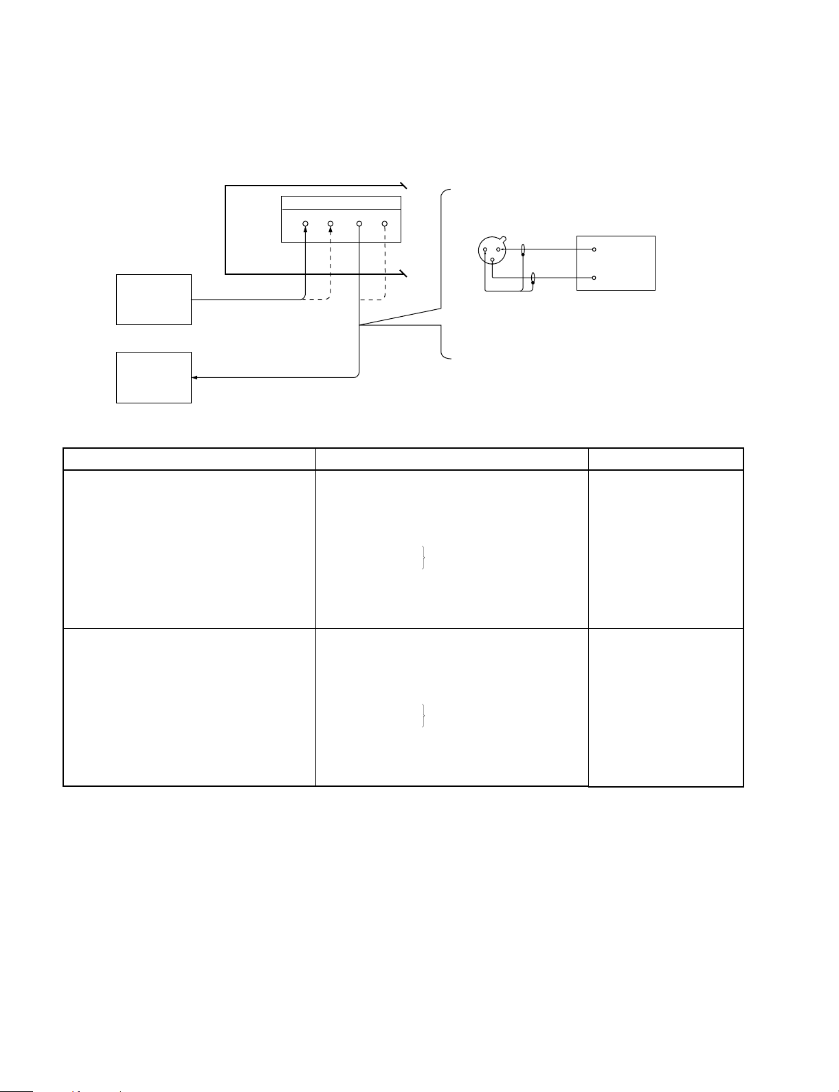
5-3-4. Output Balance Adjustment
Connection
Rear panel
CH1CH2
Audio analyzer
AF oscillator
Oscilloscope
Adjustment procedure
ANALOG
INPUT
OUTPUT
CH1
CH2
ANALOG
OUTPUT CH-1, CH-2
1
2
3
Oscilloscope
CH 1
CH 2
CH 1; 1 V/div
CH 2; 1 V/div
ADD mode; ON
1 ms/div
Adjustment condition
Step 1
. Input the 1 kHz, +4 dBs (0 dBs = 0.775 Vrms)
signal to the ANALOG INPUT CH-1 connector.
. Connect an oscilloscope to the ANALOG
OUTPUT CH-1 connector as follows:
Oscilloscope ANALOG OUTPUT
CH-1 connector
CH-1 → Across pin-2 and pin-1 (GND)
CH-2 → Across pin-3 and pin-1 (GND)
Step 2
. Input the 1 kHz, +4 dBs (0 dBs = 0.775 Vrms)
signal to the ANALOG INPUT CH-2 connector.
. Connect an oscilloscope to the ANALOG
OUTPUT CH-2 connector as follows:
Oscilloscope ANALOG OUTPUT
CH-2 connector
CH-1 → Across pin-2 and pin-1 (GND)
CH-2 → Across pin-3 and pin-1 (GND)
Output balance between + (pin-2) and _ (pin-3) of
the ANALOG OUTPUT CH-1 :
Adjustment procedure
Oscilloscope CH-1
Oscilloscope CH-2
Adjust 1RV105 until amplitude of the ADDed
waveform is 34.6 mVp-p or less.
Output balance between + (pin-2) and _ (pin-3) of
the ANALOG OUTPUT CH-2 :
Adjustment procedure
Oscilloscope CH-1
Oscilloscope CH-2
Adjust 1RV205 until amplitude of the ADDed
waveform is 34.6 mVp-p or less.
Specification
1% or less *
ADD mode ON
1% or less *
ADD mode ON
Adjustment (SSP-11 board)
1RV105 (F3)
1RV205 (E3)
* : Output balance between + (pin-2) and _ (pin-3) of the ANALOG OUTPUT must be 1%, means that the amplitude of
the ADDed waveform must be 34.6 mVp-p or less when the amplitude before ADDition is 3.46 Vp-p (+4 dBs).
5-12(E)
PCM-7040
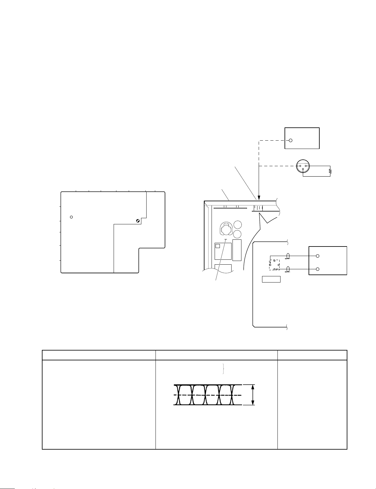
5-4. Time Code Output Level Adjustment
To perform the adjustment, first remove the top plate.
Perform the adjustment when SSP-11 board and TC block
components are replaced, or if time code output level is to
be changed.
1. Adjustment for board No. suffix -11
Equipment and Tools
Oscilloscope
Pre-recorded time code DAT tape
XLR 3PIN (female) connector
10 kZ 1/4 W resistor
Adjustment Location
A2BC D E F GH
1
E3 (A2)
3
4
5
6
RV701 (F3)
SSP-11 board (A-side)
Board No. 1-663-709-11
Switch and control setting
Same as “5-1-2. Switch and Control Initial Setting”.
Connection
TC OUTPUT
Rear panel
E3(A2),SSP-11 board
Equipment used
TC INPUT
or
12
XLR 3PIN (female)
connector
-WIRING SIDE-
CP-268 board (B-side)
CN57
4
E3/SSP-11
1
2
3
TC OUT
E3/SSP-11
OUT(+)
3
OUT(
-
)
Oscilloscope
CH1
CH2
CH1,2 : 0.5V/div
100us/div
INVERT : ON
ADD : ON
10kZ
Adjustment Procedure
Adjustment Condition
. Connect a 10 kZ dummy load (See “Connec-
tion”.) or equipment (for using time code) to the
TIME CODE OUTPUT (rear panel) connector.
. Connect the oscilloscope as follows:
Oscilloscope Connect to
CH1 → 2pin, TC OUT connector
(CPU-268 board)
E3 (A2), GND
CH2 → 3pin, TC OUT connector
(CPU-268 board)
E3 (A2), GND
. Insert the pre-recorded time code DAT tape
and playback tape (PLAY mode).
PCM-7040
Specification
Oscilloscope CH-1
Oscilloscope CH-2; INVERT
Both channels:
ADD mode
A
A = 2.4 Vp-p
. If the time code output level is to be changed,
adjust 1RV701 so that voltage A above becomes
the desired voltage.
Adjustment (SSP-11 board)
1RV701 (F3)
5-13(E)
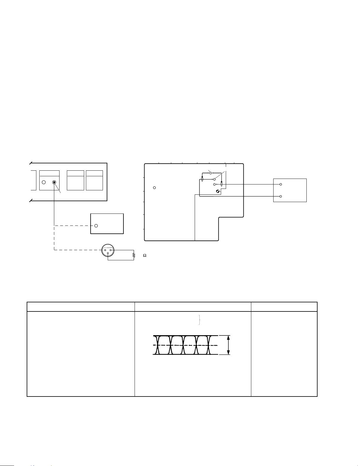
2. Adjustment for board No. suffix -12 and higher
Equipment and Tools
Oscilloscope
Pre-recorded time code DAT tape
XLR 3PIN (female) connector
10 kZ 1/4 W resistor
Switch and control setting
Same as “5-1-2. Switch and Control Initial Setting”.
Connection/Adjustment Location
Rear panel
TIME CODE
OUTPUT
Equipment used
TC INPUT
or
3
12
XLR3 pin(female)
connector
-WIRING SIDE-
Adjustment Procedure
Adjustment Condition
. Connect a 10 kZ dummy load (See “Connec-
tion”.) or equipment (for using time code) to the
TIME CODE OUTPUT (rear panel) connector.
OUT(+)
OUT(
A2BC D E F GH
1
E3 (A2)
3
4
5
6
10k
-
)
Oscilloscope CH-1
Oscilloscope CH-2; INVERT
E1 (F1)
TP73
(F2)
TP74 (F2)
RV701 (F3)
SSP-11board (A-side)
Board No.1-663-709-12 and higher
Specification
Both channels:
ADD mode
Oscilloscope
CH 1
CH 2
CH 1, 2 ; 0.5 V/div
INVERT; ON
ADD
100 µs/div
; ON
Adjustment (SSP-11 board)
1RV701 (F3)
. Connect the oscilloscope as follows:
Oscilloscope Connect to
CH1 → TP73 (F2)
E1 (F1), GND
CH2 → TP74 (F2)
E1 (F1), GND
. Insert the pre-recorded time code DAT tape
and playback tape (PLAY mode).
5-14(E)
A
A = 2.4 Vp-p
. If the time code output level is to be changed,
adjust 1RV701 so that voltage A above becomes
the desired voltage.
PCM-7040

6-1. Notes on Repair Parts
1. Safety Related Components Warning
Components marked ! are critical to safe operation.
Therefore, specified parts should be used in the case of
replacement.
2. Standardization of Parts
Some repair parts supplied by Sony differ from those
used for the unit. These are because of parts
commonality and improvement.
Parts list has the present standardized repair parts.
3. Stock of Parts
Parts marked with “o” at SP (Supply Code) column of
the spare parts list may be not stocked. Therefore, the
delivery date will be delayed.
Section 6
Spare Parts
4. Units Representation
The following represented units are changed or omitted
in writing.
Units Representation
Capacitance uFuF
Inductance uHuH
Resistance Z Abbreviation
Temperature dC XXX-DEG-C
PCM-7040
6-1
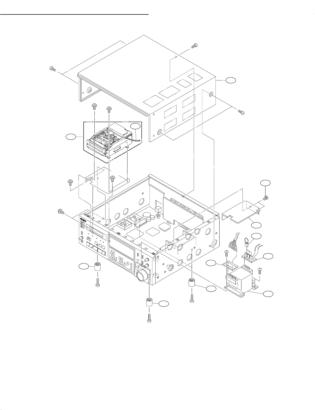
MD ASSY/POWER TRANSFORMER/ TOP PLATE
6-2. Exploded Views
B4 x 6
B3 x 6
8
PWH3 x 6
PWH3 x 6
1
PWH3 x 6
9
PWH3 x 6
B4 x 6
5
PWH3 x 6
10
7
6
B4 x 6
3
4
B4 x 6
B4 x 20
9
No. Part No. SP Description
B4 x 20
1 A-8311-799-A s MD ASSY
2 ! 1-429-937-11 s TRANSFORMER, POWER
3 1-663-710-11 o PRINTED WIRING BOARD, PS-451
4 1-663-711-11 o PRINTED WIRING BOARD, PS-452
5 1-956-633-11 o HARNESS, SUB (RF2)
6 1-956-640-11 o HARNESS, SUB (CN)
7 3-191-386-01 o INSULATING SHEET
8 3-191-392-01 o PLATE, TOP
9 3-642-656-01 s FOOT
10 4-818-403-00 s RIVET, NYLON
6-2
9
2
B4 x 20
PCM-7040
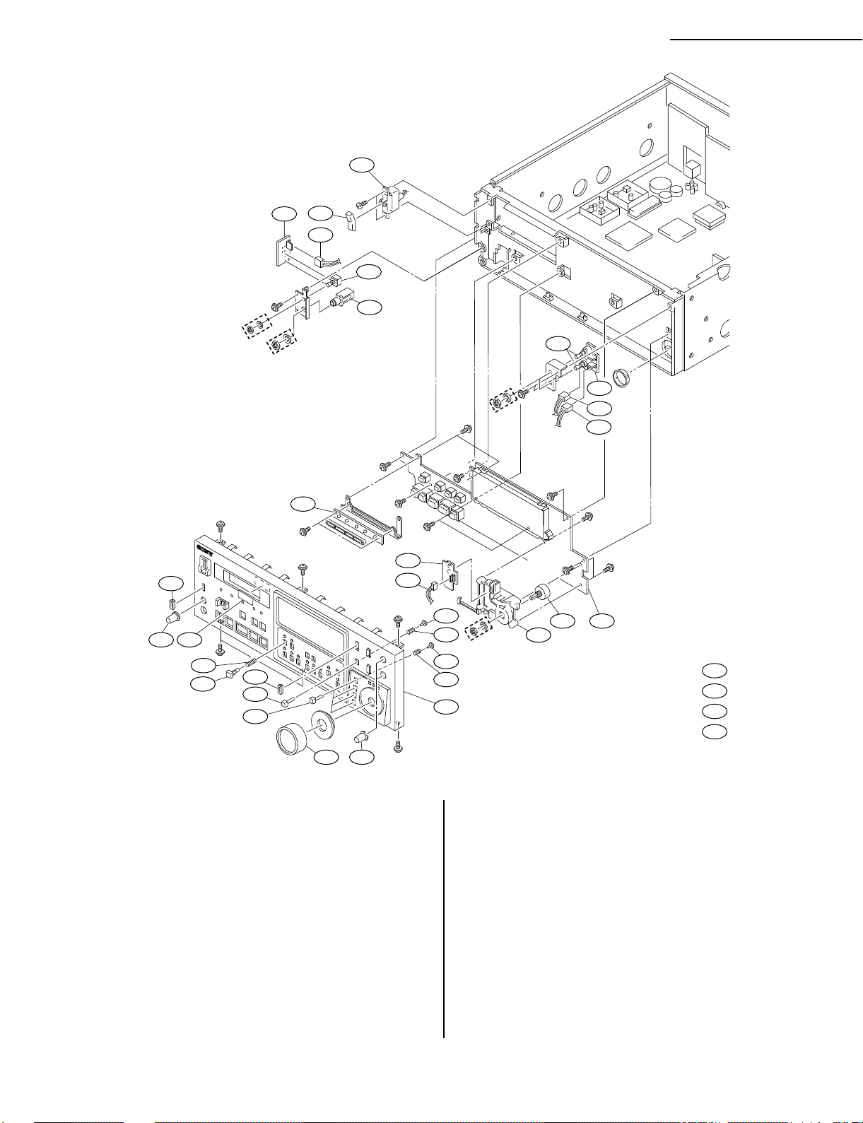
112
FRONT PANEL ASSY
109
B3 x 6
125
117
105
103
118
122
PWH3 x 6
126
119
PWH3 x 6
*1
PWH3 x 6
118
120
120
*2
PWH3 x 5
110
PWH3 x 6
PWH3 x 6
PWH3 x 6
102 103
108
111
114
PWH3 x 6
PWH
3 x 6
PWH3 x 6
PWH
3 x 5
124
123
124
123
104
PWH
3 x 6
106
PWH
3 x 6
*3
PWH
3 x 6
PWH3 x 6
*4
121
113
115
116
PWH3 x 6
107 101
PWH3 x 6
*1: Supplied with 105
*2: Supplied with 108
*3: Supplied with 106
*4: Supplied with 107
No. Part No. SP Description No. Part No. SP Description
101 A-8311-410-A o KY-192A MOUNTED CIRCUIT BOARD 116 1-956-644-11 o HARNESS, SUB (REC VR2)
102 X-3165-315-3 s DIAL ASSY 117 1-956-645-11 o HARNESS, SUB (HP)
103 X-3167-823-1 s KNOB ASSY (P), VOL 118 3-166-928-02 o ESCUTCHEON, SW
104 X-3167-892-2 s PANEL ASSY, FRONT 119 3-166-929-11 o KEY TOP (LARGE)
105 1-241-331-11 s RES, VAR, CARBON 10K/10K 120 3-166-930-01 o KEY TOP (SMALL)
106 1-241-332-11 s RES, VAR, CARBON 20K 121 3-167-806-03 o TABLE, ENCORDER
107 1-466-955-11 s ENCODER, ROTARY 122 3-184-994-01 o ISR STICKER (S)
108 1-507-863-51 s JACK, LARGE TYPE 123 3-567-099-01 o SPRING, COMPRESSION
109 ! 1-762-953-11 s SWITCH, POWER 124 3-668-009-02 o PIN, PUSH BUTTON
110 1-637-269-11 o PRINTED WIRING BOARD, LED-104 125 3-688-814-01 s CAP, SWITCH
111 1-637-270-11 o PRINTED WIRING BOARD, SW-420 126 4-862-354-00 s SPRING, COMPRESSION
112 1-637-283-14 o PRINTED WIRING BOARD, HP-48
113 1-637-284-13 o PRINTED WIRING BOARD, VR-109
114 1-946-966-11 o HARNESS (SW)
115 1-956-643-11 o HARNESS, SUB (REC VR1)
PCM-7040
6-3
 Loading...