

Sony MJL21195, MJL21195G, MJL21196, MJL21196G Service Manual
MJL21195, MJL21196
Preferred Device
Silicon Power Transistors
The MJL21195 and MJL21196 utilize Perforated Emitter
technology and are specifically designed for high power audio output,
disk head positioners and linear applications.
• Total Harmonic Distortion Characterized
• High DC Current Gain − h
• Excellent Gain Linearity
• High SOA: 2.50 A, 80 V, 1 Second
• Epoxy Meets UL 94, V−0 @ 0.125 in
• ESD Ratings: Human Body Model, 3B u 8000 V
Machine Model, C u 400 V
• Pb−Free Packages are Available*
= 25 Min @ IC = 8 Adc
FE
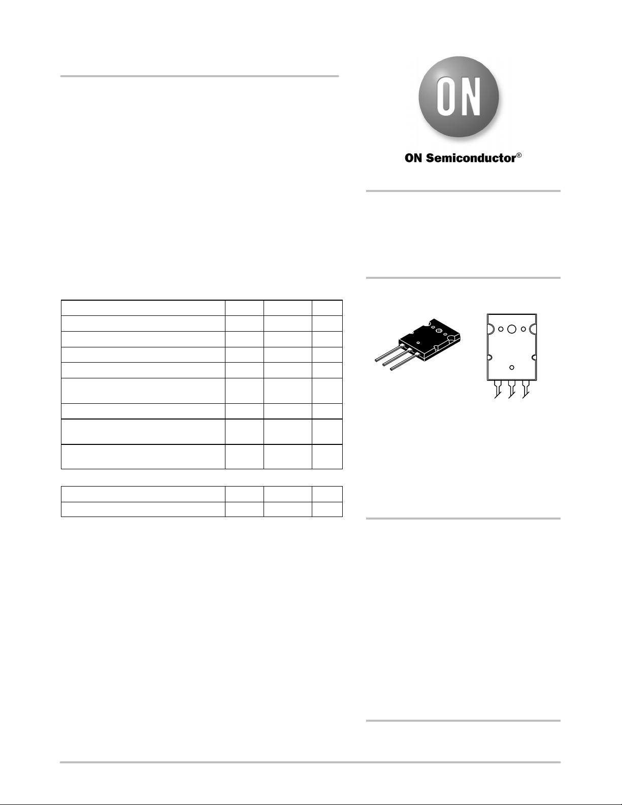
http://onsemi.com
16 A COMPLEMENTARY
SILICON POWER
TRANSISTORS
250 V, 200 W
MAXIMUM RATINGS
Rating Symbol Value Unit
Collector−Emitter Voltage V
Collector−Base Voltage V
Emitter−Base Voltage V
Collector−Emitter Voltage − 1.5 V V
Collector Current − Continuous
Collector Current − Peak (Note 1)
Base Current − Continuous I
Total Power Dissipation @ TC = 25°C
Derate Above 25°C
Operating and Storage Junction
Temperature Range
TJ, T
CEO
CBO
EBO
CEX
I
C
B
P
D
stg
250 Vdc
400 Vdc
5 Vdc
400 Vdc
16
30
5 Adc
200
1.43
− 65 to
+150
Adc
W
W/°C
°C
THERMAL CHARACTERISTICS
Characteristic Symbol Max Unit
Thermal Resistance, Junction−to−Case
Maximum ratings are those values beyond which device damage can occur.
Maximum ratings applied to the device are individual stress limit values (not
normal operating conditions) and are not valid simultaneously. If these limits are
exceeded, device functional operation is not implied, damage may occur and
reliability may be affected.
1. Pulse Test: Pulse Width = 5.0 ms, Duty Cycle ≤10%.
R
q
JC
0.7 °C/W
MARKING
DIAGRAM
MJLxxxx
AYYWWG
TO−264
CASE 340G
STYLE 2
xxxx = 21195 or 21196
A = Assembly Location
WL, L = Wafer Lot
YY, Y = Year
WW, W = Work Week
G= Pb−Free Package
ORDERING INFORMATION
See detailed ordering and shipping information in the package
dimensions section on page 6 of this data sheet.
*For additional information on our Pb−Free strategy and soldering details, please
download the ON Semiconductor Soldering and Mounting Techniques
Reference Manual, SOLDERRM/D.
© Semiconductor Components Industries, LLC, 2005
June, 2005 − Rev. 3
1 Publication Order Number:
Preferred devices are recommended choices for future use
and best overall value.
MJL21195/D
MJL21195, MJL21196
ELECTRICAL CHARACTERISTICS (T
= 25°C unless otherwise noted)
C
Characteristic
OFF CHARACTERISTICS (Note 2)
Collector−Emitter Sustaining Voltage
(IC = 100 mAdc, IB = 0)
Collector Cutoff Current
(VCE = 200 Vdc, IB = 0)
OFF CHARACTERISTICS (Note 3)
Emitter Cutoff Current
(VCE = 5 Vdc, IC = 0)
Collector Cutoff Current
(VCE = 250 Vdc, V
BE(off)
= 1.5 Vdc)
SECOND BREAKDOWN (Note 3)
Second Breakdown Collector Current with Base Forward Biased
(VCE = 50 Vdc, t = 1 s (Nonrepetitive)
(VCE = 80 Vdc, t = 1 s (Nonrepetitive)
ON CHARACTERISTICS (Note 3)
DC Current Gain
(IC = 8 Adc, VCE = 5 Vdc)
(IC = 16 Adc, IB = 5 Adc)
Base−Emitter On Voltage
(IC = 8 Adc, VCE = 5 Vdc)
Collector−Emitter Saturation Voltage
(IC = 8 Adc, IB = 0.8 Adc)
(IC = 16 Adc, IB = 3.2 Adc)
DYNAMIC CHARACTERISTICS (Note 3)
Total Harmonic Distortion at the Output
V
= 28.3 V, f = 1 kHz, P
RMS
LOAD
= 100 W
RMS
unmatched
(Matched pair hFE = 50 @ 5 A/5 V) hFE
matched
Current Gain Bandwidth Product
(IC = 1 Adc, VCE = 10 Vdc, f
= 1 MHz)
test
Output Capacitance
(VCB = 10 Vdc, IE = 0, f
= 1 MHz)
test
2. Pulse Test: Pulse Width = 5.0 ms, Duty Cycle ≤10%.
3. Pulse Test: Pulse Width = 300 ms, Duty Cycle ≤2%.
Symbol Min Typical Max Unit
V
CEO(sus)
I
CEO
I
EBO
I
CEX
I
S/b
h
FE
V
BE(on)
V
CE(sat)
T
h
FE
HD
f
T
C
ob
250 − − Vdc
− − 100
− − 100
− − 100
mAdc
mAdc
mAdc
Adc
4.0
2.25
25
8.0
−
−
−
−
−
−
100
−
− − 2.2 Vdc
Vdc
−
−
−
−
1.4
4
%
−
−
0.8
0.08
−
−
4 − − MHz
− − 500 pF
, CURRENT BANDWIDTH PRODUCT (MHz)
T
F
6.5
6.0
5.5
5.0
4.5
4.0
3.5
3.0
2.5
2.0
PNP MJL21195 NPN MJL21196
VCE = 10 V
VCE = 5 V
TJ = 25°C
f
= 1 MHz
test
1.0 100.1
IC, COLLECTOR CURRENT (A)
Figure 1. Typical Current Gain
Bandwidth Product
7.5
7.0
6.5
6.0
5.5
5.0
4.5
4.0
3.5
3.0
2.5
2.0
, CURRENT BANDWIDTH PRODUCT (MHz)
1.5
T
F
1.0
http://onsemi.com
2
VCE = 5 V
TJ = 25°C
f
= 1 MHz
test
1.0 100.1
IC, COLLECTOR CURRENT (A)
Figure 2. Typical Current Gain
Bandwidth Product
VCE = 10 V
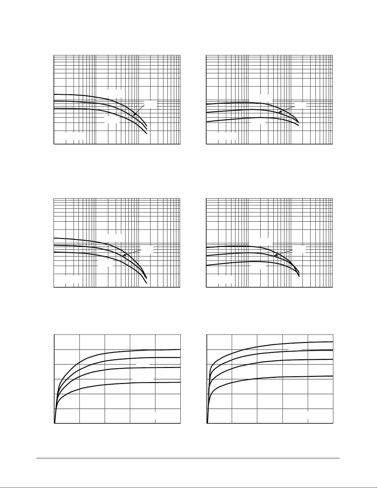
1000
MJL21195, MJL21196
TYPICAL CHARACTERISTICS
PNP MJL21195 NPN MJL21196
1000
100
, DC CURRENT GAIN
FE
h
1000
100
, DC CURRENT GAIN
FE
h
10
VCE = 20 V
TJ = 100°C
25°C
−25 °C
IC, COLLECTOR CURRENT (A)
100
, DC CURRENT GAIN
FE
h
VCE = 20 V
100101.00.1
10
TJ = 100°C
25°C
−25 °C
IC, COLLECTOR CURRENT (A)
Figure 3. DC Current Gain, VCE = 20 V Figure 4. DC Current Gain, VCE = 20 V
PNP MJL21195
TJ = 100°C
−25 °C
25°C
1000
100
, DC CURRENT GAIN
FE
h
NPN MJL21196
TJ = 100°C
25°C
−25 °C
100101.00.1
, COLLECTOR CURRENT (A)
I
VCE = 5 V
10
IC, COLLECTOR CURRENT (A)
Figure 5. DC Current Gain, V
= 5 V Figure 6. DC Current Gain, VCE = 5 V
CE
100101.00.1
PNP MJL21195
30
25
20
15
10
C
5.0
0
0
5.0 10 15 20 25
VCE, COLLECTOR−EMITTER VOLTAGE (V)
2.0 A
1.5 A
1.0 A
IB = 0.5 A
TJ = 25°C
, COLLECTOR CURRENT (A)
I
C
Figure 7. Typical Output Characteristics
VCE = 5 V
10
IC, COLLECTOR CURRENT (A)
NPN MJL21196
30
25
20
15
10
5.0
0
0
5.0 10 15 20 25
VCE, COLLECTOR−EMITTER VOLTAGE (V)
Figure 8. Typical Output Characteristics
100101.00.1
2.0 A
1.5 A
1.0 A
IB = 0.5 A
TJ = 25°C
http://onsemi.com
3
 Loading...