

Sony MJH11017, MJH11019, MJH11021, MJH11018, MJH11020 Service Manual
...
MJH11017, MJH11019,
MJH11021(PNP)
MJH11018, MJH11020,
MJH11022(NPN)
Preferred Device
Complementary Darlington
Silicon Power Transistors
These devices are designed for use as general purpose amplifiers,
low frequency switching and motor control applications.
Features
• High DC Current Gain @ 10 Adc — h
• Collector−Emitter Sustaining Voltage
V
CEO(sus)
= 150 Vdc (Min) — MJH11018, 17
= 200 Vdc (Min) — MJH11020, 19
= 250 Vdc (Min) — MJH11022, 21
• Low Collector−Emitter Saturation Voltage
V
= 1.2 V (Typ) @ IC = 5.0 A
CE(sat)
= 1.8 V (Typ) @ I
• Monolithic Construction
• Pb−Free Packages are Available*
MAXIMUM RATINGS
Rating
Collector−Emitter Voltage
Collector−Base Voltage
Emitter−Base Voltage
Collector Current − Continuous
Base Current
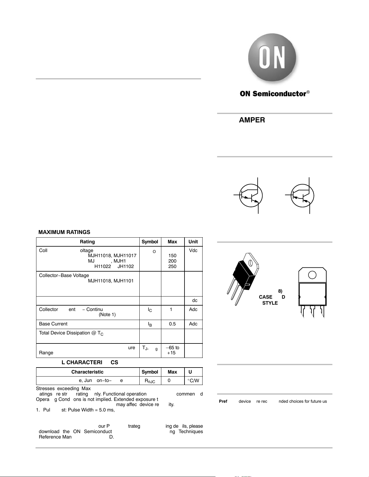
Total Device Dissipation @ TC = 25_C
Derate above 25_C
Operating and Storage Junction Temperature
Range
THERMAL CHARACTERISTICS
Thermal Resistance, Junction−to−Case
Stresses exceeding Maximum Ratings may damage the device. Maximum
Ratings are stress ratings only. Functional operation above the Recommended
Operating Conditions is not implied. Extended exposure to stresses above the
Recommended Operating Conditions may affect device reliability.
1. Pulse Test: Pulse Width = 5.0 ms, Duty Cycle v 10%.
MJH11018, MJH11017
MJH11020, MJH11019
MJH11022, MJH11021
MJH11018, MJH11017
MJH11020, MJH11019
MJH11022, MJH11021
− Peak (Note 1)
Characteristic
= 400 Min (All Types)
FE
= 10 A
C
Symbol
V
CEO
V
CB
V
EB
I
C
I
B
P
TJ, T
Symbol
R
q
D
JC
stg
Max
–65 to
+150
Max
0.83
150
200
250
150
200
250
5.0
15
30
0.5
150
1.2
Unit
Vdc
Vdc
Vdc
Adc
Adc
W
W/_C
_C
Unit
_C/W
http://onsemi.com
15 AMPERE DARLINGTON
COMPLEMENTARY SILICON
POWER TRANSISTORS
150−250 VOLTS, 150 WATTS
NPN PNP
BASE
1
COLLECTOR 2
EMITTER 3
MJH11019
MJH11021
MARKING
DIAGRAM
AYWWG
MJH110xx
COLLECTOR 2
BASE
1
EMITTER 3
MJH11018 MJH11017
MJH11020
MJH11022
SOT−93
(TO−218)
1
2
3
A = Assembly Location
Y = Year
WW = Work Week
G=Pb−Free Package
MJH110xx = Device Code
CASE 340D
STYLE 1
xx = 17, 19, 21, 18, 20, 22
ORDERING INFORMATION
See detailed ordering and shipping information in the package
dimensions section on page 6 of this data sheet.
Preferred devices are recommended choices for future use
and best overall value.
*For additional information on our Pb−Free strategy and soldering details, please
download the ON Semiconductor Soldering and Mounting Techniques
Reference Manual, SOLDERRM/D.
© Semiconductor Components Industries, LLC, 2008
September, 2008 − Rev. 7
1 Publication Order Number:
MJH11017/D
MJH11017, MJH11019, MJH11021 (PNP) MJH11018, MJH11020, MJH11022 (NPN)
160
140
120
100
80
60
40
, POWER DISSIPATION (WATTS)
D
20
P
0
0
40 60 100 120 16080 14020
, CASE TEMPERATURE (°C)
T
C
Figure 1. Power Derating
ELECTRICAL CHARACTERISTICS (T
= 25_C unless otherwise noted)
C
Characteristic
OFF CHARACTERISTICS
Collector−Emitter Sustaining Voltage (Note 2)
(I
= 0.1 Adc, IB = 0) MJH11017, MJH11018
C
MJH11019, MJH11020
MJH11021, MJH11022
Collector Cutoff Current
(VCE = 75 Vdc, IB = 0) MJH11017, MJH11018
(VCE = 100 Vdc, IB = 0) MJH11019, MJH11020
(VCE = 125 Vdc, IB = 0) MJH11021, MJH11022
Collector Cutoff Current
(V
= Rated VCB, V
CE
= Rated VCB, V
(V
CE
= 1.5 Vdc)
BE(off)
= 1.5 Vdc, TJ = 150_C)
BE(off)
Emitter Cutoff Current (VBE = 5.0 Vdc IC = 0)
ON CHARACTERISTICS (Note 2)
DC Current Gain
(I
= 10 Adc, VCE = 5.0 Vdc)
C
(IC = 15 Adc, VCE = 5.0 Vdc)
Collector−Emitter Saturation Voltage
(I
= 10 Adc, IB = 100 mA)
C
= 15 Adc, IB = 150 mA)
(I
C
Base−Emitter On Voltage (IC = 10 A, VCE = 5.0 Vdc)
Base−Emitter Saturation Voltage (IC = 15 Adc, IB = 150 mA)
DYNAMIC CHARACTERISTICS
Current−Gain Bandwidth Product (IC = 10 Adc, VCE = 3.0 Vdc, f = 1.0 MHz)
Output Capacitance MJH11018, MJH11020, MJH11022
(V
= 10 Vdc, IE = 0, f = 0.1 MHz) MJH11017, MJH11019, MJH11021
CB
Small−Signal Current Gain (IC = 10 Adc, VCE = 3.0 Vdc, f = 1.0 kHz)
SWITCHING CHARACTERISTICS
Characteristic
Delay Time
Rise Time
Storage Time
(VCC = 100 V, IC = 10 A, IB = 100 mA
V
= 5.0 V) (See Figure 2)
BE(off)
Fall Time
2. Pulse Test: Pulse Width = 300 ms, Duty Cycle v 2.0%.
Symbol
V
CEO(sus)
I
CEO
I
CEV
I
EBO
h
FE
V
CE(sat)
V
BE(on)
V
BE(sat)
f
T
C
ob
h
fe
Symbol
t
d
t
r
t
s
t
f
Min
150
200
250
−
−
−
−
−
−
400
100
−
−
−
−
3.0
−
−
75
NPN
150
1.2
4.4
2.5
Typical
Max
−
−
−
1.0
1.0
1.0
0.5
5.0
2.0
15,000
−
2.5
4.0
2.8
3.8
−
400
600
−
PNP
75
0.5
2.7
2.5
Unit
Vdc
mAdc
mAdc
mAdc
−
Vdc
Vdc
Vdc
−
pF
−
Unit
ns
ms
ms
ms
http://onsemi.com
2
MJH11017, MJH11019, MJH11021 (PNP) MJH11018, MJH11020, MJH11022 (NPN)
V
CC
100 V
R
C
TUT
RB & RC varied to obtain desired current levels
D
, must be fast recovery types, e.g.:
1
1N5825 used above I
MSD6100 used below I
1.0
0.7
D = 0.5
0.5
0.3
0.2
0.2
0.1
0.1
0.05
0.07
0.02
0.05
0.03
RESISTANCE (NORMALIZED)
SINGLE PULSE
0.02
r(t), EFFECTIVE TRANSIENT THERMAL
0.01
0.02
0.01 0.03 3.0 30 3000.3
≈ 100 mA
B
≈ 100 mA
B
0.01
0.05 1.0 2.0 5.0 10 20 50 100 200 500
0.1 0.50.2
, tf ≤ 10 ns
t
r
Duty Cycle = 1.0%
Figure 2. Switching Times Test Circuit
V2
APPROX
+12 V
0
V1
APPROX
-8.0 V
For NPN test circuit, reverse diode and voltage polarities.
R
q
JC
R
q
JC
D CURVES APPLY FOR POWER
PULSE TRAIN SHOWN
READ TIME AT t
T
J(pk)
t, TIME (ms)
25 ms
(t) = r(t) R
q
(pk)
JC
1
R
q
= 0.83°C/W MAX
- TC = P
51
(t)
JC
R
B
D
1
+4.0 V
For t
and tr, D1 is disconnected
d
and V2 = 0
P
(pk)
DUTY CYCLE, D = t1/t
t
1
t
2
SCOPE
2
1000
30
20
10
5.0
2.0
1.0
0.5
, COLLECTOR CURRENT (AMPS)
C
I
0.2
0
= 25°C SINGLE PULSE
T
C
0.5 ms
1.0 ms
5.0 ms
WIRE BOND LIMIT
THERMAL LIMIT
SECOND BREAKDOWN LIMIT
MJH11017, MJH11018
MJH11019, MJH11020
MJH11021, MJH11022
2.0
5.0 50 25015030
3.0 10
V
, COLLECTOR-EMITTER VOLTAGE (VOLTS)
CE
dc
20 100
Figure 4. Maximum Rated Forward Bias
Safe Operating Area (FBSOA)
Figure 3. Thermal Response
FORWARD BIAS
0.1 ms
There are two limitations on the power handling ability of
a transistor: average junction temperature and second
breakdown. Safe operating area curves indicate I
limits of the transistor that must be observed for reliable
operation; i.e., the transistor must not be subjected to greater
dissipation than the curves indicate.
The data of Figure 4 is based on T
variable depending on conditions. Second breakdown pulse
limits are valid for duty cycles to 10% provided T
v 150_C. T
Figure 3. At high case temperatures, thermal limitations will
reduce the power that can be handled to values less than the
limitations imposed by second breakdown.
= 150_C; TC is
J(pk)
may be calculated from the data in
J(pk)
C
− V
CE
J(pk)
http://onsemi.com
3
 Loading...