

Sony MJE270, MJE270G, MJE271, MJE271G Service Manual
MJE270 (NPN),
MJE271 (PNP)
Complementary Silicon
Power Transistors
Features
• High Safe Operating Area
@ 40 V, 1.0 s = 0.375 A
I
S/B
• Collector−Emitter Sustaining Voltage
V
CEO(sus)
= 100 Vdc (Min)
• High DC Current Gain
@ 120 mA, 10 V = 1500 (Min)
h
FE
• Pb−Free Packages are Available*
MAXIMUM RATINGS
Rating
Collector−Emitter Voltage
Collector−Base Voltage
Emitter−Base Voltage
Collector Current − Continuous
− Peak
Base Current
Total Power Dissipation @ TC = 25_C
Derate above 25_C
Total Power Dissipation @ TA = 25_C
Derate above 25_C
Operating and Storage Junction
Temperature Range
THERMAL CHARACTERISTICS
Characteristic
Thermal Resistance, Junction−to−Case
Thermal Resistance, Junction−to−Ambient
Maximum ratings are those values beyond which device damage can occur.
Maximum ratings applied to the device are individual stress limit values (not normal
operating conditions) and are not valid simultaneously. If these limits are exceeded,
device functional operation is not implied, damage may occur and reliability may be
affected.
Symbol
V
CEO
V
CB
V
EB
I
C
I
B
P
D
P
D
TJ, T
stg
Symbol
R
q
JC
R
q
JA
Value
100
100
5.0
2.0
4.0
0.1
15
0.12
1.5
0.012
−65 to +150
Max
8.33
83.3
Unit
Vdc
Vdc
Vdc
Adc
Adc
W
W/_C
W
W/_C
_C
Unit
_C/W
_C/W
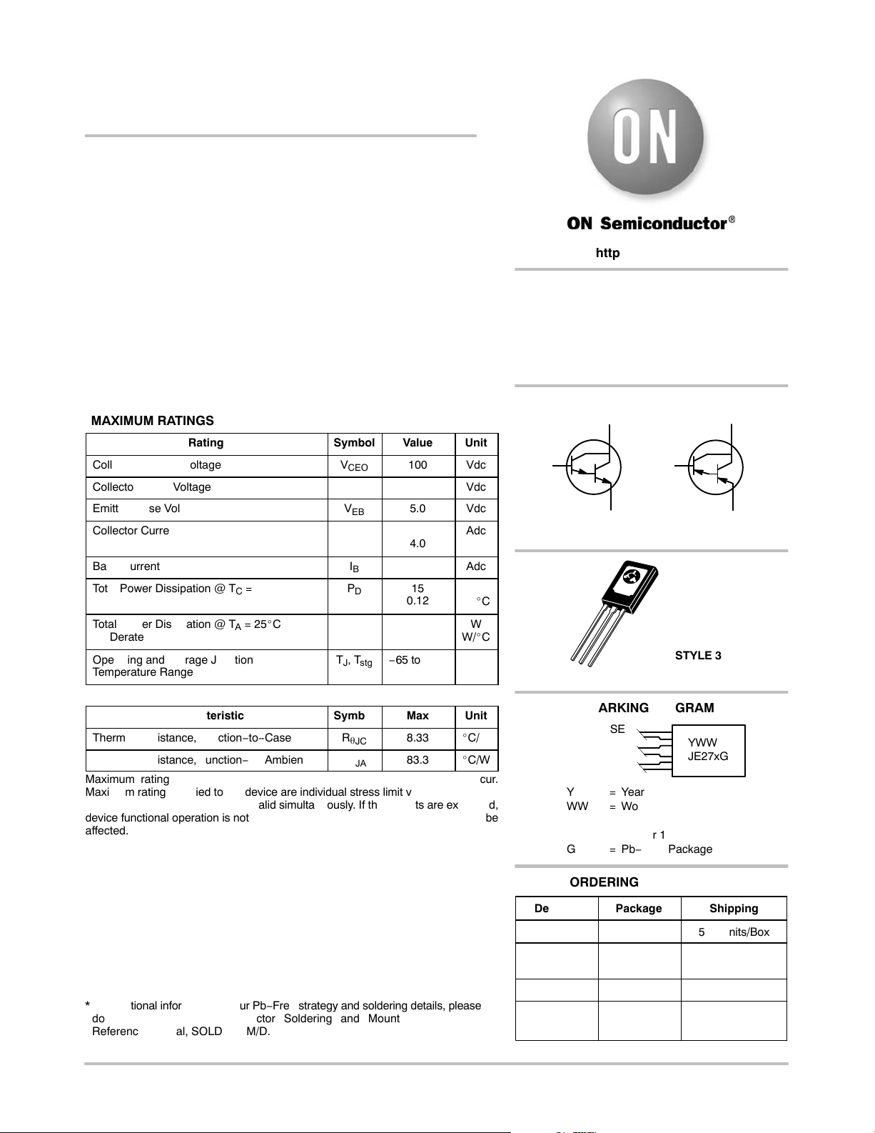
http://onsemi.com
2.0 AMPERE
COMPLEMENTARY
POWER DARLINGTON
TRANSISTORS
100 VOLTS, 15 WATTS
NPN PNP
COLLECTOR 2
BASE
1
EMITTER 3
MJE270 MJE271
3
2
1
MARKING DIAGRAM
1 BASE
2 COLLECTOR
3 EMITTER
Y = Year
WW = Work Week
JE27x = Specific Device Code
G=Pb−Free Package
BASE
1
x= 0 or 1
COLLECTOR 2
EMITTER 3
TO−225
CASE 77
STYLE 3
YWW
JE27xG
*For additional information on our Pb−Free strategy and soldering details, please
download the ON Semiconductor Soldering and Mounting Techniques
Reference Manual, SOLDERRM/D.
© Semiconductor Components Industries, LLC, 2008
September, 2008 − Rev. 7
1 Publication Order Number:
ORDERING INFORMATION
Device Package Shipping
MJE270 TO−225
MJE270G TO−225
(Pb−Free)
MJE271 TO−225 500 Units/Box
MJE271G TO−225
(Pb−Free)
500 Units/Box
500 Units/Box
500 Units/Box
MJE270/D

MJE270 (NPN), MJE271 (PNP)
ELECTRICAL CHARACTERISTICS (T
= 25_C unless otherwise noted)
C
Characteristic
OFF CHARACTERISTICS
Collector−Emitter Sustaining Voltage (Note 1)
(I
= 10 mAdc, IB = 0)
C
Collector Cutoff Current
(V
= 100 Vdc, IB = 0)
CE
Collector Cutoff Current
(VCB = 100 Vdc, IE = 0)
Emitter Cutoff Current
(V
= 5.0 Vdc, IC = 0)
BE
SECOND BREAKDOWN
Second Breakdown Collector Current with Base Forward Biased
(V
= 40 Vdc, t = 1.0 s, Non−repetitive)
CE
ON CHARACTERISTICS (Note 1)
DC Current Gain
(I
= 20 mAdc, VCE = 3.0 Vdc)
C
(IC = 120 mAdc, VCE = 10 Vdc)
Collector−Emitter Saturation Voltage
(I
= 20 mAdc, IB = 0.2 mAdc)
C
(IC = 120 mAdc, IB = 1.2 mAdc)
Base−Emitter On Voltage
(I
= 120 mAdc, VCE = 10 Vdc)
C
DYNAMIC CHARACTERISTICS
Current Gain − Bandwidth Product (Note 2)
(IC = 0.05 Adc, VCE = 5.0 Vdc, f
= 1.0 MHz)
test
1. Pulse Test: Pulse Width v 300 ms, Duty Cycle v 2.0%.
2. f
= ⎪hfe⎪• f
T
test
.
Symbol
V
CEO(sus)
I
CEO
I
CBO
I
EBO
I
S/b
h
FE
V
CE(sat)
V
BE(on)
f
T
Min
100
−
−
−
375
500
1500
−
−
−
6.0
Max
−
1.0
0.3
0.1
−
−
−
2.0
3.0
2.0
−
Unit
Vdc
mAdc
mAdc
mAdc
Adc
−
Vdc
Vdc
MHz
10,000
, DC CURRENT GAIN
FE
h
7000
5000
3000
1000
700
500
300
100
150°C
25°C
-55°C
0.05 0.3 1.0 1.5
0.03 0.070.015 0.5
0.1 0.7
IC, COLLECTOR CURRENT (AMPS)
Figure 1. DC Current Gain
VCE = 3.0 V
, COLLECTOR CURRENT (AMPS)
C
I
http://onsemi.com
2
5.0
1.0
0.5
0.1
0.05
0.01
10
dc
MJE270/MJE271
BONDING WIRE LIMIT
THERMAL LIMIT @ T
= 25°C
C
(SINGLE PULSE)
SECOND BREAKDOWN LIMIT
1.0
3.0 30 70
V
, COLLECTOR-EMITTER VOLTAGE (VOLTS)
CE
7.0 10
100
Figure 2. Safe Operating Area
 Loading...