

Sony MJ11021, MJ11022 Service Manual
MJ11021(PNP)
MJ11022 (NPN)
Complementary Darlington
Silicon Power Transistors
Complementary Darlington Silicon Power Transistors are designed
for use as general purpose amplifiers, low frequency switching and
motor control applications.
Features
• High dc Current Gain @ 10 Adc − h
• Collector−Emitter Sustaining Voltage
V
CEO(sus)
= 250 Vdc (Min) − MJ11022, 21
• Low Collector−Emitter Saturation
V
CE(sat)
• 100% SOA Tested @ V
= 1.0 V (Typ) @ IC = 5.0 A
= 1.8 V (Typ) @ I
= 44 V
CE
= 4.0 A
I
C
t = 250 ms
• Pb−Free Packages are Available*
= 400 Min (All Types)
FE
= 10 A
C
http://onsemi.com
15 AMPERE
COMPLEMENTARY
DARLINGTON POWER
TRANSISTORS
250 VOLTS, 175 WATTS
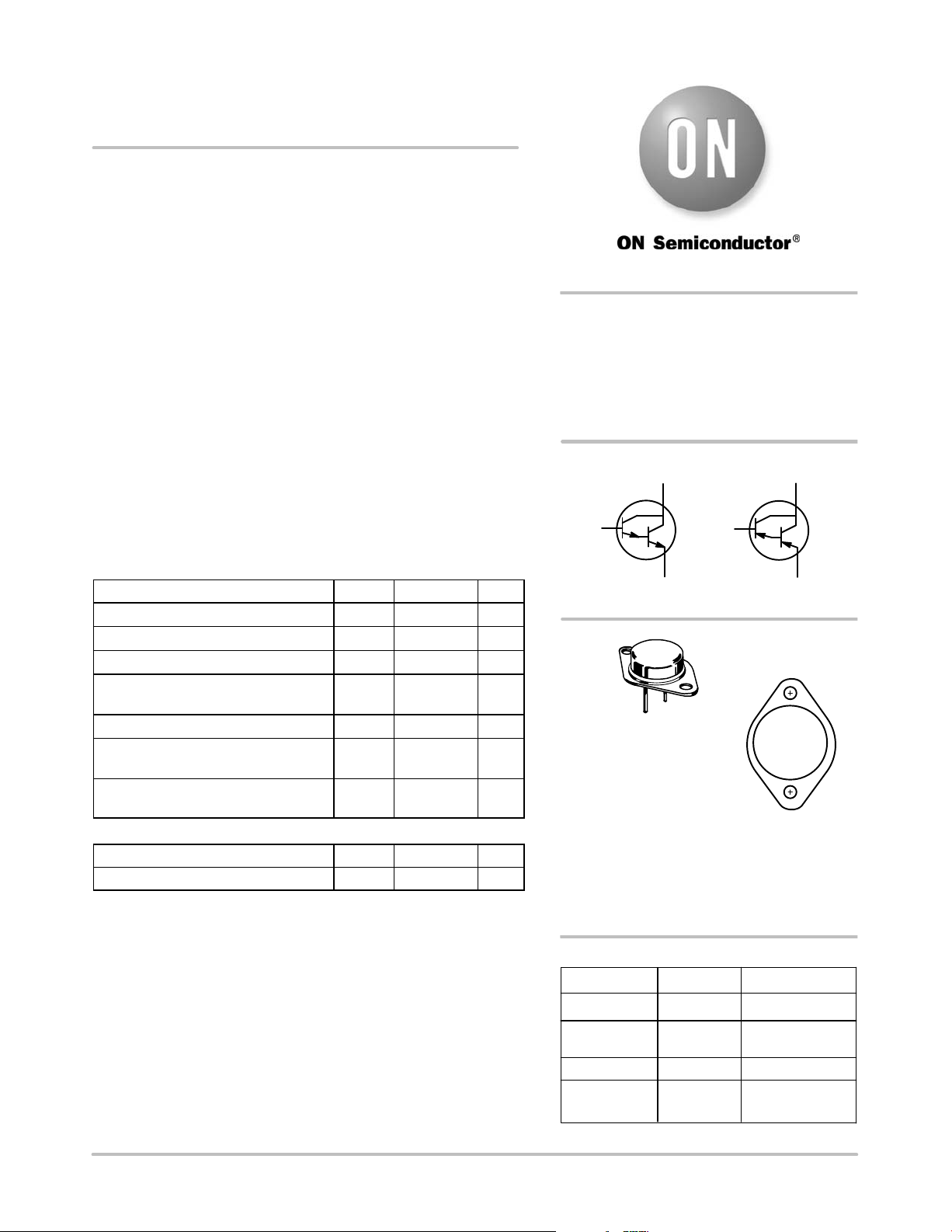
NPN PNP
COLLECTOR
CASE
BASE
1
BASE
1
COLLECTOR
CASE
MAXIMUM RATINGS (T
Rating
Collector−Emitter Voltage V
Collector−Base Voltage V
Emitter−Base Voltage V
Collector Current − Continuous
Base Current I
Total Power Dissipation @ TC = 25°C
Derate Above 25°C
Operating and Storage Junction
Temperature Range
= 25°C unless otherwise noted)
J
− Peak (Note 1)
Symbol Value Unit
CEO
CBO
EBO
I
P
TJ, T
C
B
D
stg
250 Vdc
250 Vdc
50 Vdc
15
30
0.5 Adc
175
1.16
– 65 to +175
− 65 to +200
Adc
W
W/°C
°C
THERMAL CHARACTERISTICS
Characteristic Symbol Max Unit
Thermal Resistance, Junction−to−Case
Maximum ratings are those values beyond which device damage can occur.
Maximum ratings applied to the device are individual stress limit values (not
normal operating conditions) and are not valid simultaneously. If these limits are
exceeded, device functional operation is not implied, damage may occur and
reliability may be affected.
1. Pulse Test: Pulse Width = 5 ms, Duty Cycle ≤ 10%.
*For additional information on our Pb−Free strategy and soldering details, please
download the ON Semiconductor Soldering and Mounting Techniques
Reference Manual, SOLDERRM/D.
R
q
JC
0.86 °C/W
EMITTER 2
MJ11022 MJ11021
EMITTER 2
MARKING
DIAGRAM
1
2
TO−204 (TO−3)
CASE 1−07
STYLE 1
MJ1102x = Device Code
x = 1 or 2
G= Pb−Free Package
A = Location Code
YY = Year
WW = Work Week
MEX = Country of Orgin
MJ1102xG
AYYWW
MEX
ORDERING INFORMATION
Device Package Shipping
MJ11021 TO−3 100 Units/Tray
MJ11021G TO−3
MJ11022 TO−3 100 Units/Tray
MJ11022G
(Pb−Free)
TO−3
(Pb−Free)
100 Units/Tray
100 Units/Tray
© Semiconductor Components Industries, LLC, 2008
September, 2008 − Rev. 3
1 Publication Order Number:
MJ11021/D
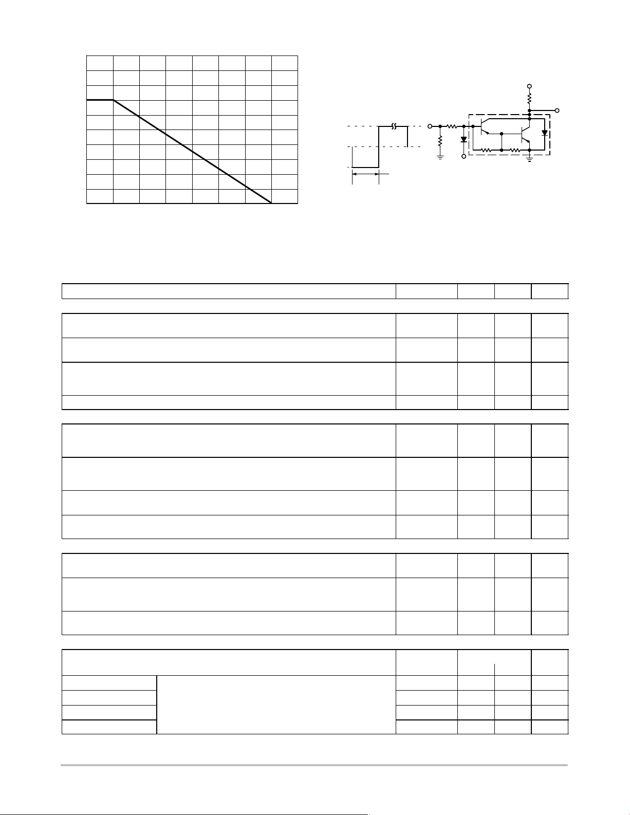
200
150
100
, POWER DISSIPATION (WATTS)
50
D
P
0
0 150 17525
MJ11021(PNP) MJ11022 (NPN)
50 75 100 125 200
TC, CASE TEMPERATURE (°C)
Figure 1. Power Derating
RB and RC VARIED TO OBTAIN DESIRED CURRENT LEVELS
D
MUST BE FAST RECOVERY TYPE, e.g.:
1
1N5825 USED ABOVE I
MSD6100 USED BELOW I
V2
APPROX
+12 V
0
V1
APPROX
-8.0 V
, tf ≤ 10 ns
t
r
DUTY CYCLE = 1.0%
25 ms
≈ 100 mA
B
≈ 100 mA
B
51
R
B
D
1
≈ 10 K ≈ 8.0
+4.0 V
for t
and tr, D1 is disconnected
d
and V2 = 0
For NPN test circuit reverse diode and voltage polarities.
Figure 2. Switching Times Test Circuit
TUT
V
100 V
R
C
CC
SCOPE
ELECTRICAL CHARACTERISTICS (T
= 25_C unless otherwise noted)
C
Characteristic Symbol Min Max Unit
OFF CHARACTERISTICS
Collector−Emitter Sustaining Voltage (Note 1)
(I
= 0.1 Adc, IB = 0) MJ11021, MJ11022
C
Collector Cutoff Current
(V
= 125, IB = 0) MJ11021, MJ11022
CE
Collector Cutoff Current
(V
= Rated VCB, V
CE
= Rated VCB, V
(V
CE
= 1.5 Vdc)
BE(off)
= 1.5 Vdc, TJ = 150_C)
BE(off)
Emitter Cutoff Current (VBE = 5.0 Vdc, IC = 0) I
ON CHARACTERISTICS (Note 1)
DC Current Gain
(I
= 10 Adc, VCE = 5.0 Vdc)
C
(IC = 15 Adc, VCE = 5.0 Vdc)
Collector−Emitter Saturation Voltage
(IC = 10 Adc, IB = 100 mA)
(IC = 15 Adc, IB = 150 mA)
Base−Emitter On Voltage
I
= 10 A, VCE = 5.0 Vdc)
C
Base−Emitter Saturation Voltage
(I
= 15 Adc, IB = 150 mA)
C
DYNAMIC CHARACTERISTICS
Current−Gain Bandwidth Product
(I
= 10 Adc, VCE = 3.0 Vdc, f = 1.0 MHz)
C
Output Capacitance (VCB = 10 Vdc, IE = 0, f = 0.1 MHz)
MJ11022
MJ11021
Small−Signal Current Gain
(IC = 10 Adc, VCE = 3.0 Vdc, f = 1.0 kHz)
SWITCHING CHARACTERISTICS
Characteristic Symbol NPN PNP Unit
Delay Time
Rise Time t
Storage Time t
(VCC = 100 V, IC = 10 A, IB = 100 mA
V
= 50 V) (See Figure 2)
BE(off)
Fall Time t
1. Pulsed Test: Pulse Width = 300 ms, Duty Cycle v 2%.
V
CEO(sus)
I
CEO
I
CEV
EBO
h
FE
V
CE(sat)
V
BE(on)
V
BE(sat)
250 −
− 1.0
−
−
0.5
5.0
− 2.0 mAdc
400
100
15,000
−
−
−
2.0
3.4
− 2.8 Vdc
− 3.8 Vdc
[hfe] 3.0 − Mhz
C
ob
h
fe
−
−
400
600
75 − −
Typical
t
d
r
s
f
150 75 ns
1.2 0.5
4.4 2.7
10.0 2.5
Vdc
mAdc
mAdc
−
Vdc
pF
ms
ms
ms
http://onsemi.com
2
 Loading...