

Sony MDSDRE-1 Service manual
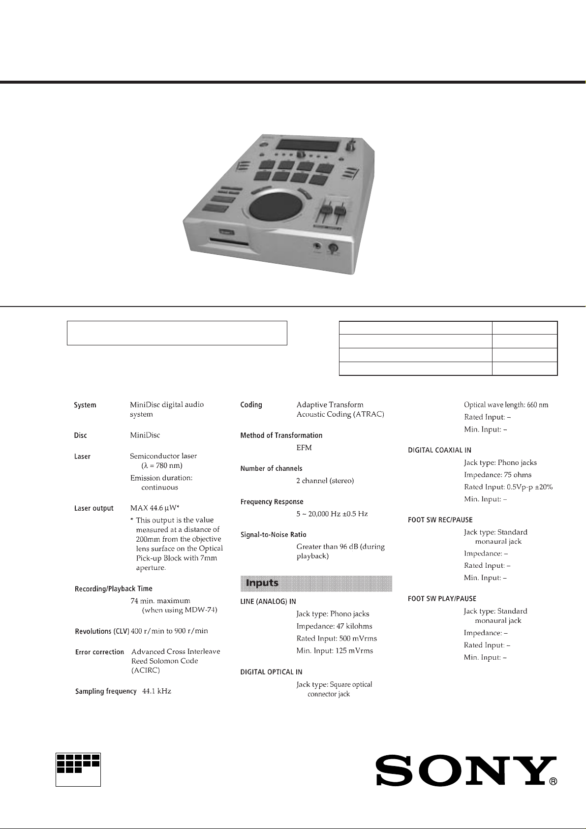
MDS-DRE1
SERVICE MANUAL
U.S. and foreign patents licensed form Dolby Laboratories
Licensing Corporation.
SPECIFICATIONS
US Model
Canadian Model
AEP Model
UK Model
Model Name Using Similar Mechanism MDS-JA3ES
MD Mechanism Type MDM-2CR
Base Unit Name MBU-2B
Optical Pick-up Name KMS-210A/J-N
MICROFILM
– Continued on next page –
MINIDISC RECORDER/PLAYER
TABLE OF CONTENTS
1. SERVICING NOTES ............................................... 3
2. GENERAL ................................................................... 7
3. DISASSEMBLY ......................................................... 9
4. TEST MODE.............................................................. 12
5. ELECTRICAL ADJUSTMENTS......................... 15
6. DIAGRAMS
6-1. Block Diagram – SERVO Section – .............................. 21
6-2. Block Diagram – MAIN Section (1/2) – ....................... 23
6-3. Block Diagram – MAIN Section (2/2) – ....................... 25
6-4. Block Diagram
– DISPLAY/KEY/POWER SUPPLY Section –............. 27
6-5. Notes for Printed Wiring Board
and Schematic Diagram .................................................. 30
6-6. Printed Wiring Board – BD Board (SIDE A) – ............. 31
6-7. Printed Wiring Board – BD Board (SIDE B) –............. 33
6-8. Schematic Diagram – BD Section (1/2) – ..................... 35
6-9. Schematic Diagram – BD Section (2/2)– ...................... 37
6-10. Printed Wiring Boards
– DETECTION SW Board, MOTOR Board –............... 39
6-11. Schematic Diagram
– DETECTION SW/MOTOR Section – ........................ 41
6-12. Printed Wiring Board – DIGITAL Board (SIDE A) – ... 43
6-13. Printed Wiring Board – DIGITAL Board (SIDE B) – ... 45
6-14. Schematic Diagram – DIGITAL Section (1/4) – .......... 47
6-15. Schematic Diagram – DIGITAL Section (2/4) – .......... 49
6-16. Schematic Diagram – DIGITAL Section (3/4) – .......... 51
6-17. Schematic Diagram – DIGITAL Section (4/4) – .......... 53
6-18. Pr inted Wiring Board – PANEL Section (1) – .............. 56
6-19. Schematic Diagram – PANEL Section (1) – ................. 57
6-20. Pr inted Wiring Boards – PANEL Section (2) – ............. 59
6-21. Schematic Diagram – PANEL Section (2) – ................. 61
6-22. Pr inted Wiring Boards – POWER Section – ................. 63
6-23. Schematic Diagram – POWER Section – ..................... 65
6-24. IC Pin Function Description ........................................... 77
SAFETY-RELATED COMPONENT WARNING!!
COMPONENTS IDENTIFIED BY MARK ! OR DOTTED
LINE WITH MARK ! ON THE SCHEMA TIC DIAGRAMS
AND IN THE PARTS LIST ARE CRITICAL TO SAFE
OPERATION. REPLACE THESE COMPONENTS WITH
SONY PARTS WHOSE PART NUMBERS APPEAR AS
SHOWN IN THIS MANUAL OR IN SUPPLEMENTS PUBLISHED BY SONY.
7. EXPLODED VIEWS................................................ 88
8. ELECTRICAL PARTS LIST ............................... 93
ATTENTION AU COMPOSANT AYANT RAPPORT
À LA SÉCURITÉ!
LES COMPOSANTS IDENTIFIÉS P AR UNE MARQUE !
SUR LES DIAGRAMMES SCHÉMATIQUES ET LA LISTE
DES PIÈCES SONT CRITIQUES POUR LA SÉCURITÉ
DE FONCTIONNEMENT. NE REMPLACER CES COMPOSANTS QUE PAR DES PIÈCES SONY DONT LES
NUMÉROS SONT DONNÉS DANS CE MANUEL OU
DANS LES SUPPLÉMENTS PUBLIÉS PAR SONY.
– 2 –
SECTION 1
SERVICING NOTES
SAFETY CHECK-OUT
After correcting the original service problem, perform the following safety check before releasing the set to the customer:
Check the antenna terminals, metal trim, “metallized” knobs,
screws, and all other exposed metal parts for AC leakage.
Check leakage as described below.
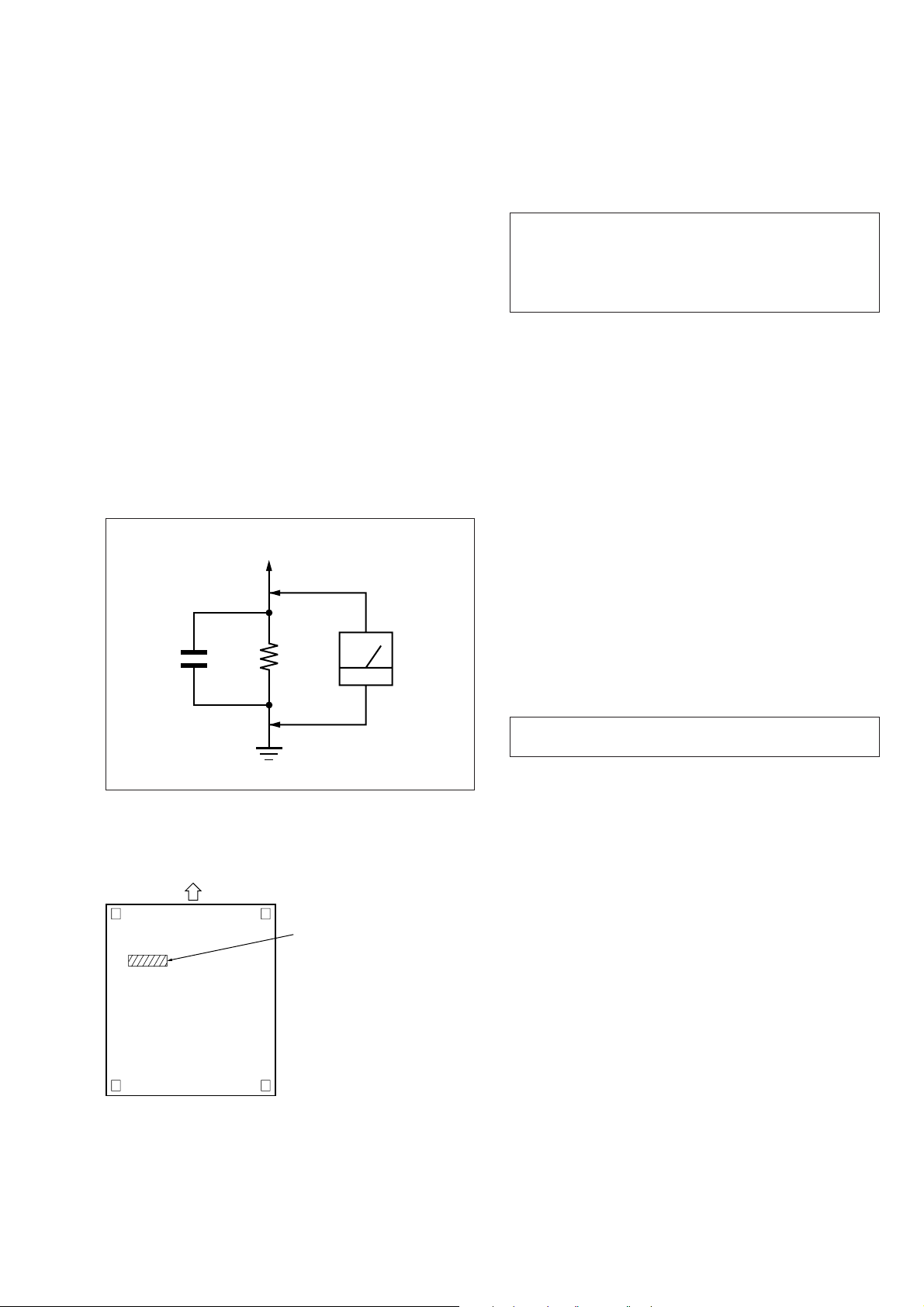
LEAKAGE TEST
The AC leakage from any exposed metal part to earth ground and
from all exposed metal parts to any exposed metal part having a
return to chassis, must not exceed 0.5 mA (500 microampers.).
Leakage current can be measured by any one of three methods.
1. A commercial leakage tester , such as the Simpson 229 or RCA
WT -540A. Follo w the manufacturers’ instructions to use these
instruments.
2. A battery-operated AC milliammeter. The Data Precision 245
digital multimeter is suitable for this job.
3. Measuring the voltage drop across a resistor by means of a
VOM or battery-operated AC voltmeter. The “limit” indication is 0.75 V, so analog meters must have an accurate lowvoltage scale. The Simpson 250 and Sanwa SH-63T rd are examples of a passive VOM that is suitable. Nearly all battery
operated digital multimeters that have a 2 V A C range are suitable. (See Fig. A)
To Exposed Metal
Parts on Set
CAUTION
Danger of explosion if battery is incorrectly replaced.
Replace only with the same or equivalent type recommended by
the manufacturer.
Discard used batteries according to the manufacturer’s instructions.
ADVARSEL!
Lithiumbatteri-Eksplosionsfare ved fejlagtig håndtering.
Udskiftning må kun ske med batteri
af samme fabrikat og type.
Levér det brugte batteri tilbage til leverandøren.
ADVARSEL
Eksplosjonsfare ved feilaktig skifte av batteri.
Benytt samme batteritype eller en tilsvarende type
anbefalt av apparatfabrikanten.
Brukte batterier kasseres i henhold til fabrikantens
instruksjoner.
VARNING
Explosionsfara vid felaktigt batteribyte.
Använd samma batterityp eller en likvärdig typ som
rekommenderas av apparattillverkaren.
Kassera använt batteri enligt gällande föreskrifter.
1.5 k
0.15 µF
Fig. A. Using an AC voltmeter to check AC leakage.
Ω
Earth Ground
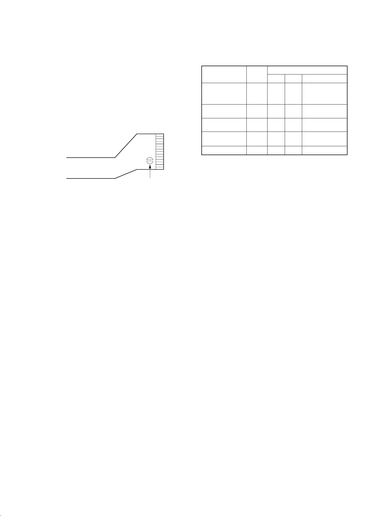
MODEL IDENTIFICATION
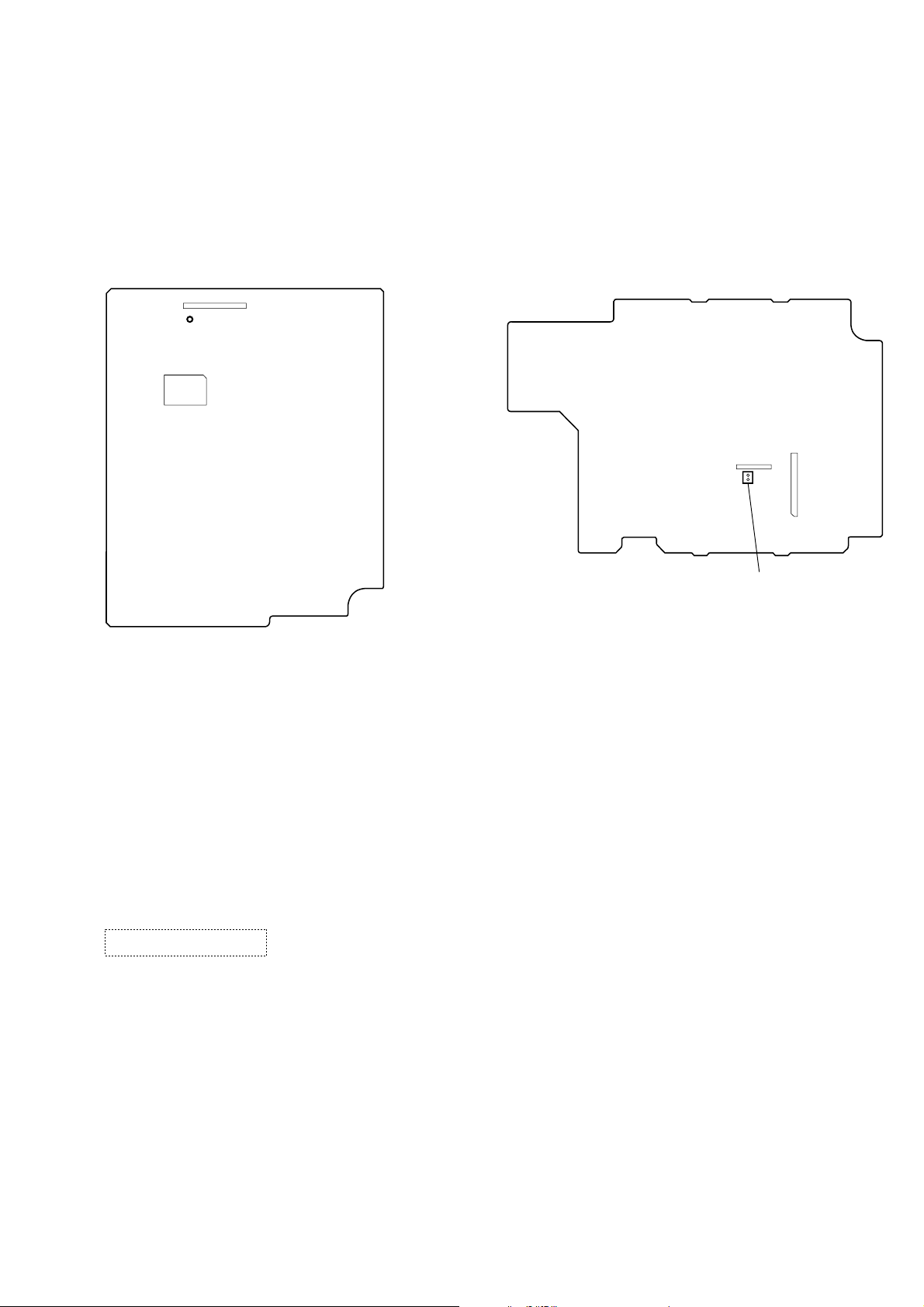
— LOWER SIDE CABINET (BOTTOM VIEW) —
Front Side
Part No.
4-210-100-1
4-210-100-2
π
: AEP and UK models
π
: US and
AC
voltmeter
(0.75 V)
Canadian models
VAROITUS
Paristo voi räjähtää, jos se on virheellisesti asennettu.
V aihda paristo ainoastaan laitev almistajan suosittelemaan tyyppiin.
Hävitä käytetty paristo valmistajan ohjeiden mukaisesti.
NOTES ON HANDLING THE OPTICAL PICK-UP
BLOCK OR BASE UNIT
The laser diode in the optical pick-up block may suffer electrostatic break-down because of the potential difference generated
by the charged electrostatic load, etc. on clothing and the human
body.
During repair, pay attention to electrostatic break-down and also
use the procedure in the printed matter which is included in the
repair parts.
The flexible board is easily damaged and should be handled with
care.
NOTES ON LASER DIODE EMISSION CHECK
The laser beam on this model is concentrated so as to be focused
on the disc reflective surface by the objective lens in the optical
pick-up block. Therefore, when checking the laser diode emission, observe from more than 30 cm away from the objective lens.
– 3 –
CAUTION
Use of controls or adjustments or performance of procedures
other than those specified herein may result in hazardous radiation exposure.
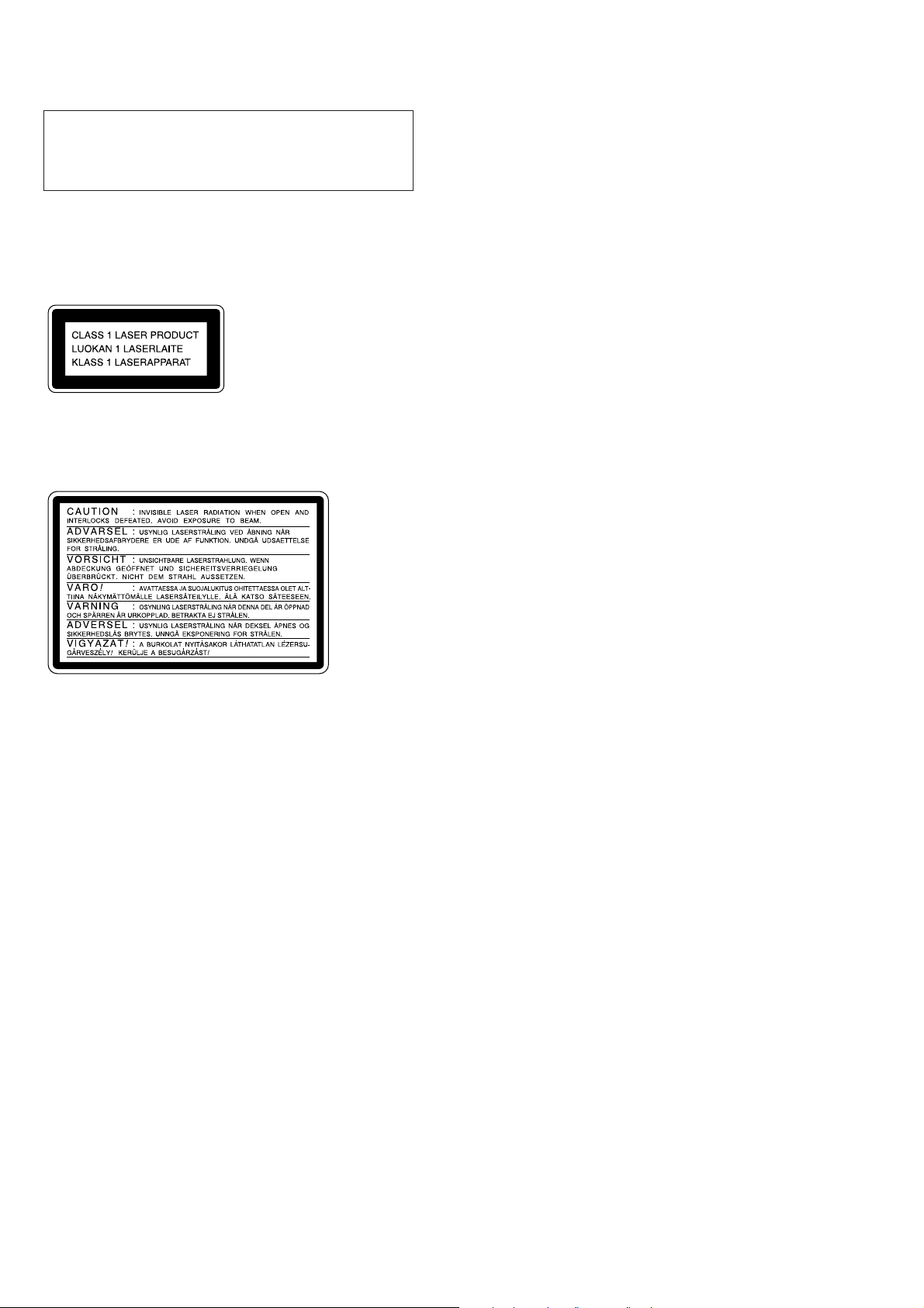
This appliance is classified as a CLASS 1 LASER product.
The CLASS 1 LASER PRODUCT MARKING is located on
the rear exterior.
Laser component in this product is capable of emitting radiation
exceeding the limit for Class 1.
The following caution label is located inside the unit.
Flexible Circuit Board Repairing
• Keep the temperature of the soldering iron around 270 ˚C during repairing.
• Do not touch the soldering iron on the same conductor of the
circuit board (within 3 times).
• Be careful not to apply force on the conductor when soldering
or unsoldering.
Notes on chip component replacement
• Never reuse a disconnected chip component.
• Notice that the minus side of a tantalum capacitor may be damaged by heat.
– 4 –
FORCED RESET
CN901
BT451
1
2
CN451
(RESET)
The system microprocessor can be reset in the following way.
Use these methods when the unit cannot be operated normally due to the overrunning of the microprocessor, etc.
Method 1:
Set TP (RESET) of the DIGITAL board to ground momentarily.
[DIGITAL board] (Side A)
CN1
TP
(RESET)
IC101
Method 2:
Disconnect the power plug, and short-circuit CN451 of the POWER
board with a pair of tweezers, etc.
[POWER board] (Component Side)
RETRY CAUSE DISPLAY MODE
• In this test mode, the causes for retry of the unit during recording can be displayed on the fluorescent display tube.
This is useful for locating the faulty part of the unit.
• The retry cause, number of retries, and number of retry errors are displayed. Each is displayed in hexadecimal number.
Method:
1. Load a recordable disc whose contents can be erased into the unit.
2. Press the [STOP] button, [EJECT] button, [PAD1] button simultaneously.
3. Press the [REC] button, and start recording.
r
§
4. The ## value increases with each retry. If an error occurs after a retry, the @@ count will also increase.
5. To exit the test mode, press the [] (POWER) button.
U
Fig. 1 Reading the Test Mode Display
R.T s ∗ ∗ c # # e @@
Fluorescent Display Tube Signs
∗ ∗ : Cause of retry
# # : Number of retries
@@: Number of retry errors
All three displays above are in hexadecimal numbers.
– 5 –
Reading the Retry Cause Display
Higher Bits Lower Bits
Hexadecimal
Bit
Binary
*1 Some displays are not used depending on the microprocessor version.
Reading the Display:
Convert the hexadecimal display into binary display. If more than two causes, they will be added.
Example
When 42 is displayed:
Higher bit : 4 = 0100 n b6
Lower bit : 2 = 0010 n b1
In this case, the retry cause is combined of “spindle is slow” and “ader5”.
84218421
b7 b6 b5 b4 b3 b2 b1 b0
00000001
00000010
00000100
00001000
00010000
00100000
01000000
10000000
Hexa-
decimal
01
02
04
08
10
20
40
80
Cause of Retry Occurring conditions
shock *1
ader5
Discontinuous address
(Not used)
FCS incorrect
IVR rec error
Spindle is slow
Access fault
When more than 3.5 shocks are detected
When ADER was counted more than
five times continuously
When ADIP address is not continuous
(Not used)
When not in focus
When ABCD signal le vel exceeds the specified r ange
When spindle rotation is detected as slow
When access operation is not performed normally
When A2 is displayed:
Higher bit : A = 1010 n b7+b5
Lower bit : 2 = 0010 n b1
The retry cause in this case is combined of “access fault”, “IVR rec error”, and “ader5”.
Hexadecimal n Binary Conversion Table
Hexadecimal Binary Hexadecimal Binary
0
1
2
3
4
5
6
7
Reference:
In this test mode, when the [PLAY/PAUSE] button is pressed, and the disc is played back, the “PLAYBACK MODE” is set.
The display becomes as shown in Fig. 2. The playback mode is not used in particular during servicing.
44 ¢¢¢¢¢¢ p
0000
0001
0010
0011
0100
0101
0110
0111
8
9
A
B
C
D
E
F
1000
1001
1010
1011
1100
1101
1110
1111
Fig. 2 Display during Playback Mode
4 : Parts No. (Name of area named on TOC)
¢¢¢¢¢¢ : Address (Physical address on disc)
p : Track mode (Copyright information of each part, information on copyright, etc.)
– 6 –
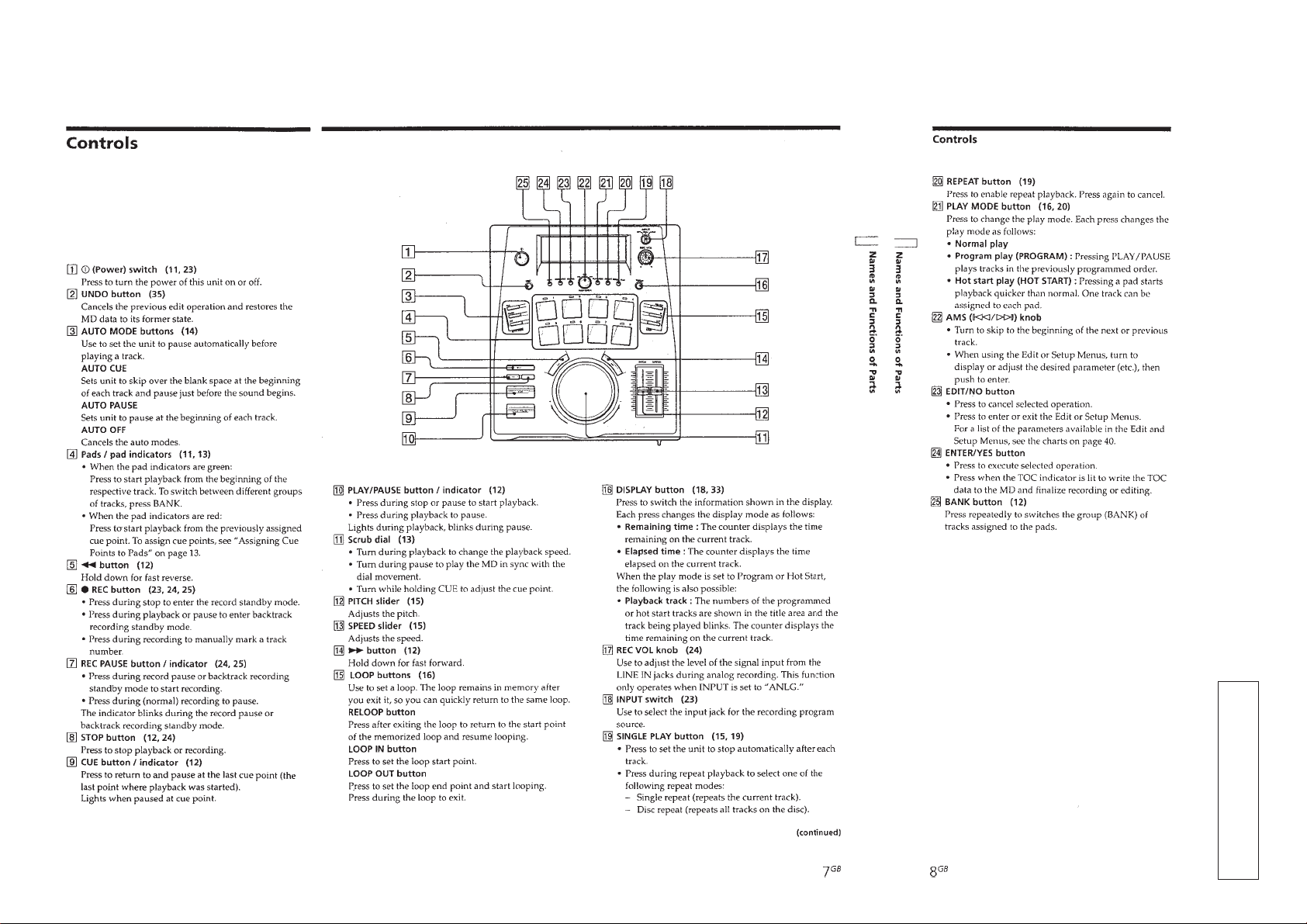
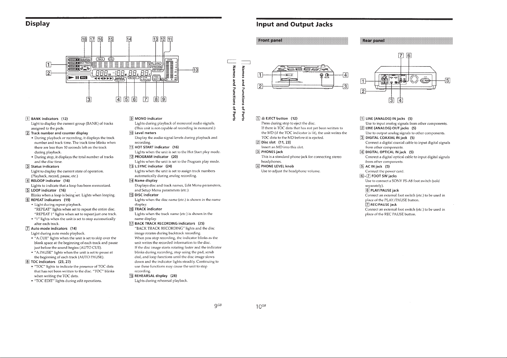
NAMES AND FUNCTIONS OF PARTS
– 7 –
SECTION 2
GENERAL
This section is extracted from
instruction manual.
– 8 –
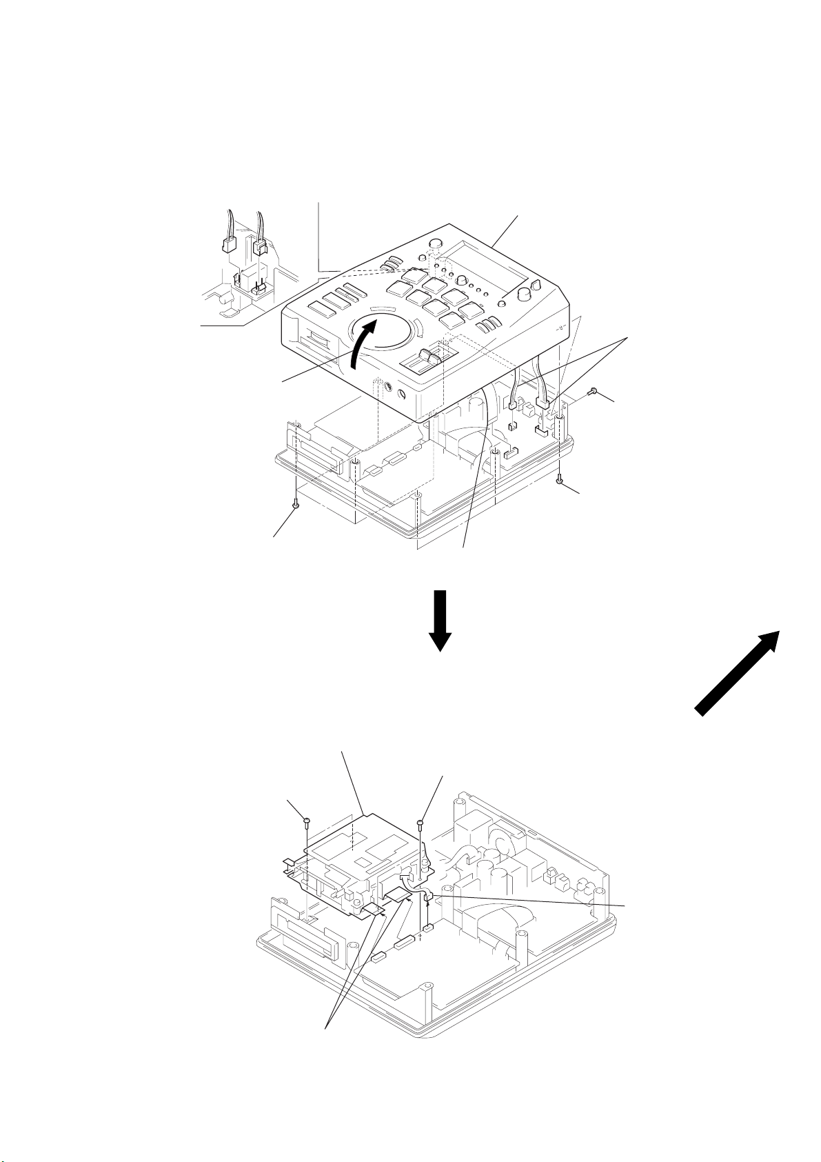
SECTION 3
s
DISASSEMBLY
Note: Follow the disassembly procedure in the numerical order given.
UPPER CABINET SECTION
4
two connectors
(CN801, 802)
3
Open the upper cabinet
section in arrow direction.
6
upper cabinet section
4
2
two screws
(BV3
two connector
(CN701, 751)
×
8)
MD ASSEMBLY
1
3
two screws
(BVTP3
five screws
(BV3
×
10)
×
8)
4
MD assembly
5
3
two screws
(BVTP3
flat wire
(CN902)
×
8)
1
three screws
(BV3
×
10)
2
two flat wires
(CN4, 5)
– 9 –
1
connector
(CN3)
BRACKET (MD)
3
two collars
4
insulator (MD)
5
compression spring
6
bracket (MD)
2
two screws
(B2.6
×
18)
1
Rotate the pully (BD) in arrow
direction
assembly in arrow direction
slider
assembly
A
and move the slider
B
B
A
.
2
two screws
(B2.6
×
18)
3
two collars
4
insulator (MD)
5
compression spring
SLIDER (M) ASSEMBLY
5
two compression
springs
C
4
two insulators (MD)
claw
B
A
claw
1
Disengage a coil spring
from the claw
2
Disengaging the claw B,
raise the lever (SLM)
upwards to remove.
3
Rotate the pully (BD) in arrow direction C.
A
.
A
– 10 –
claw
C
B
Move the claw C on the slider
4
up to the base groove in arrow
direction
direction
Base groove
A
, and raise it in arrow
B
to remove.
BASE UNIT AND LOADING MOTOR ASSEMBLY
r
1
screw
(BV3
×
6)
3
belt
4
two screws
(B2.6
×
5)
6
loading moto
assembly
2
base unit
SLIDER ASSEMBLY MOUNTING
B
1
two screws
(BV3
×
6)
3
Move the slider assembly in
arrow direction
to the lever (SLM).
A
B
, and lock it
1
Rotate fully the lever (SLM)
in arrow direction
A
5
.
connector
(CN192)
C
– 11 –
2
Rotate the pully (BD)
in arrow
C
direction.

SECTION 4
TEST MODE
4-1. Setting the Test Mode
U
Press [] (POWER) switch while pressing the [AMS] knob to turn POWER ON.
4-2. Exiting the Test Mode
Press the [REPEAT] button. Unplug the power plug from an outlet.
4-3. Basic Operations of the Test Mode
All operations are performed using the [AMS] knob, [ENTER/YES] button, and [EDIT/NO] button.
The functions of these buttons are as follows.
Function
[AMS] knob
[ENTER/YES] button
[EDIT/NO] button
Changes parameters and modes
Proceeds onto the next step. Finalizes input.
Returns to previous step. Stops operations.
Contents
4-4. Selecting the Test Mode
Eight test modes are selected by turning the [AMS] knob.
Display
TEMP ADJUS
LDPWR ADJUS
EFBAL ADJUS
FBIAS ADJUS
FBIAS CHECK
CPLAY MODE
CREC MODE
EEP MODE
For detailed description of each adjustment mode, refer to 5. Electrical Adjustments.
If a different adjustment mode has been selected by mistake, press the
* The EEP MODE is not used in servicing. If set accidentally, press the [EDIT/NO] button immediately to exit it.
4-4-1. Operating the Continuous Playback Mode
1. Entering the continuous playback mode
1 Set the disc in the unit (either MO or CD).(MO: Recordable disc, CD: Disc for playback only)
2 Rotate the [AMS] knob and display “CPLAY MODE”.
3 Press the [ENTER/YES] button to change the display to “CPLAY IN”.
4 When access completes, the display changes to “C1 = AD = ”.
Note: The “ ” displayed are arbitrary numbers.
2. Changing the parts to be played back
1 Press the [ENTER/YES] button during continuous playback to change the display to “CPLAY MID”, “CPLAY OUT”.
When pressed another time, the parts to be played back can be changed.
2 When access completes, the display changes to “C1 = AD = ”.
Note: The “ ” displayed are arbitrary numbers.
3. Ending the continuous playback mode
1 Press the [EDIT/NO] button. The display will change to “CPLAY MODE”.
2 Press the [EJECT] button and remove the disc.
Note 1: The playback start addresses for IN, MID, and OUT are as follows.
§
IN 40h cluster
MID 300h cluster
OUT 700h cluster
Temperature compensation offset adjustment
Laser power adjustment
Traverse adjustment
Focus bias adjustment
Focus bias check
Continuous playback mode
Continuous recording mode
Non-volatile memory mode *
Contents
[EDIT/NO] button to exit from it.
– 12 –

4-4-2. Operating the Continuous Recording Mode
1. Entering the continuous recording mode
1 Set the MO disc in the unit.
2 Rotate the [AMS] knob and display “CREC MODE”.
3 Press the [ENTER/YES] button to change the display to “CREC IN”.
4 When access completes, the display changes to “CREC ( ” and REC lights up.
Note : The “ ” displayed are arbitrary numbers.
2. Changing the parts to be recorded
1 When the [ENTER/YES] button is pressed during continuous recording, the display changes to “CREC MID”, “CREC OUT” and
REC goes off.
When pressed another time, the parts to be recorded can be changed.
2 When access completes, the display changes to “CREC ( ” and REC lights up.
Note : The “ ” displayed are arbitrary numbers.
3. Ending the continuous recording mode
1 Press the [EDIT/NO] button. The display changes to “CREC MODE” and REC goes off.
2 Press the [EJECT] button and remove the disc.
Note 1: The recording start addresses for IN, MID, and OUT are as follows.
§
IN 40h cluster
MID 300h cluster
OUT 700h cluster
Note 2: The [EDIT/NO] button can be used to stop recording anytime.
Note 3: During the test mode, the erasing-protection tab will not be detected. Therefore be careful not to set the continuous recording mode when a
Note 4: Do not perform continuous recording for long periods of time above 5 minutes.
Note 5: During continuous recording, be careful not to apply vibration.
disc not to be erased is set in the unit.
4-4-3. Non-Volatile Memory Mode (EEP MODE)
This mode reads and writes the contents of the non-volatile memory.
It is not used in servicing. If set accidentally, press the [EDIT/NO] button immediately to exit it.
4-5. Functions of Other buttons
Function
PLAY/PAUSE
STOP
)
0
r REC
BANK
PLAY MODE
DISPLAY
Note: The erasing-protection tab is not detected during the test mode. Recording will start regardless of the position of the erasing-protection tab when the
r
[REC] button is pressed.
Sets continuous playback when pressed in the STOP state. When pressed during continuous playback, the tracking serv o
turns ON/OFF.
Stops continuous playback and continuous recording.
The sled moves to the outer circumference only when this is pressed.
The sled moves to the inner circumference only when this is pressed.
Turns recording ON/OFF when pressed during continuous playback.
Switches between the pit and groove modes when pressed.
Switches the spindle servo mode (CLVS and A).
Switches the display when pressed.Returns to previous step. Stops operations.
Contents
– 13 –
4-6. Test Mode Displays
Each time the [DISPLAY] button is pressed, the display changes in the following order.
MODE display n Error rate display n Address display
1. MODE display
Displays “TEMP ADJUS”, “CPLAY MODE”, etc.
2. Error rate display
Error rates are displayed as follows.
C1 = AD =
C1 = : Indicates C1 error
AD = : Indicates ADER
3. Address display
Addresses are displayed as follows.
“h = s = ” (MO pit and CD)
“h = a = ” (MO groove)
h = : Header address
s = : SUBQ address
a = :ADIP address
Note: “—” is displayed when the address cannot be read.
4-7. Meanings of Other Displays
Display
·
P
REC
CLOCK
TRACK
DISC
DA TE
A. PAUSE
A – B
Light
During continuous playback
Tracking servo OFF
Recording mode ON
CLV LOCK
Pit
High reflection
CLV-S
ABCD adjustment completed
Focus auto gain successful
Tracking auto gain successful
STOP
Tracking servo ON
Recording mode OFF
CLV UNLOCK
Groove
Low reflection
CLV-A
Contents
Off
Blinking
Focus auto gain successful
Tracking auto gain failed
4-8. Precautions for Use of Test Mode
1 As loading related operations will be performed regardless of the test mode operations being performed, be sure to check that the disc is
stopped before setting and removing it.
Even if the [EJECT] button is pressed while the disc is rotating during continuous playback, continuous recording, etc., the disc will not
stop rotating.
Therefore, it will be ejected while rotating.
Always press the [EDIT/NO] button first before pressing the [EJECT] button.
2 The erasing-protection tab is not detected in the test mode. Therefore, when modes which output the recording laser power such as
continuous recording mode and traverse adjustment mode, etc. are set, the recorded contents will be erased regardless of the position of
the tab. When using a disc that is not to be erased in the test mode, be careful not to enter the continuous recording mode and traverse
adjustment mode.
§
§
– 14 –
SECTION 5
ELECTRICAL ADJUSTMENTS
Precautions for Checking Laser Diode Emission
T o check the emission of the laser diode during adjustments, never
view directly from the top as this may lose your eye-sight.
Precautions for Use of optical pick-up (KMS-210A)
As the laser diode in the optical pick-up is easily damaged by
static electricity, solder the laser tap of the flexible board when
using it.Before disconnecting the connector, desolder first. Before connecting the connector, be careful not to remove the solder.
Also take adequate measures to prevent damage by static electricity. Handle the flexible board with care as it breaks easil y.
laser tap
Optical pick-up flexible board
• Abbreviation
MO: Recordable disc
CD: Disc for playback only
Precautions for Adjustments
1) When replacing the following parts, perform the adjustments
and checks with ® in the order shown in the following table.
Optical
Pick-up
1. Temperature
compensation
offset adjustment
2. Laser power
adjustment
3. Trav erse
adjustment
4. Focus bias
adjustment
5. Error rate check
IC171
G
¬
¬¬
¬¬ ¬
¬
¬
GG
¬¬
2) Set the test mode when performing adjustments.
After completing the adjustments, exit the test mode.
3) Perform the adjustments in the order shown.
4) Use the following tools and measuring devices.
• Check Disc (MD) TDYS-1 (Parts No. 4-963-646-01)
• Laser power meter LPM-8001 (Parts No. J-2501-046-A) or
MD Laser power meter 8010S (Parts No. J-2501-145-A)
• Oscilloscope
• Digital voltmeter
• Thermometer
5) When observing several signals on the oscilloscope, etc.,
make sure that VC and ground do not connect inside the oscilloscope.
(VC and ground will become short-circuited.)
BD Board
IC101, IC121, IC191
D101
¬¬
¬
G
G
G
¬
Laser power meter
When performing laser power checks and adjustment (electrical
adjustment), use of the new MD laser power meter 8010S (J-2501145-A) instead of the conventional laser power meter is convenient.
It sharply reduces the time and trouble to set the laser power meter
sensor onto the objective lens of the pick-up.
Creating Continuously Recorded Disc
* This disc is used in focus bias adjustment and error rate check.
The following describes how to create a continuous recording
disc.
1. Insert a MO disc (blank disc) commercially available.
2. Rotate the
[AMS] knob and display “CREC MODE”.
3. Press the [ENTER/YES] button and display “CREC IN”.
4. Press the [ENTER/YES] button again to display “CREC MID”.
“CREC (0300” is displayed for a moment and recording starts.
5. Complete recording within 5 minutes.
6. Press the [EDIT/NO] button and stop recording .
7. Press the [EJECT] button and remove the MO disc.
§
The above has been how to create a continuous recording data for
the focus bias adjustment and error rate check.
Note:
• Be careful not to apply vibration during continuous recording.
– 15 –

Temperature Compensation Offset Adjustment
r
Laser Power Adjustment
Save the temperature data at that time in the non-volatile memory
as 25 ˚C reference data.
Note:
1. Usually, do not perform this adjustment.
2. Perform this adjustment in an ambient temperature of 22 ˚C to 28 ˚C.
Perform it immediately after the power is turned on when the internal
temperature of the unit is the same as the ambient temperature.
3. When D101 has been replaced, perform this adjustment after the temperature of this part has become the ambient temperature.
Adjusting Method:
1. Rotate the [AMS] knob and display “TEMP ADJUS”.
2. Press the [ENTER/YES] button and select the “TEMP ADJUS”
mode.
3. “TEMP = ” and the current temperature data will be displayed.
4. To save the data, press the [ENTER/YES] button.
When not saving the data, press the [EDIT/NO] button.
5. When the [ENTER/YES] button is pressed, “TEMP = SAV”
will be displayed for some time, followed by “TEMP ADJUS”.
When the [EDIT/NO] button is pressed, “TEMP ADJUS” will
be displayed.
Specifications:
The “TEMP = ” should be within “E0 - EF”, “F0 - FF”, “00 0F”, “10 - 1F” and “20 - 2F”.
Connection:
Laser power
meter
Optical pick-up
objective lens
Digital voltmete
BD board
TP57 (I + 5V)
TP58 (IOP)
Adjusting Method:
1. Set the laser power meter on the objective lens of the optical
pick-up. (When it cannot be set properly , press the [] but-
)
ton or [] button and move the optical pick-up.)
0
Connect the digital volt meter to TP58 (IOP) and TP57 (I+5V).
2. Rotate the [AMS] knob and display “LDPWR ADJUS”.
(Laser power : For adjustment)
3. Press the [ENTER/YES] button twice and display “LD $ 4B =
3.5 mW”.
4. Adjust RV102 of the BD board so that the reading of the laser
power meter becomes 3.4 mW.
+ 0.1
– 0
5. Press the [ENTER/YES] button and display “LD $ 96 = 7.0
mW”.
(Laser power: MO writing)
6. Check that the laser power meter and digital voltmeter readings satisfy the specified value.
Specification:
Laser power meter reading: 7.0 ± 0.3 mW
Digital voltmeter reading: Optical pickup displayed value ± 10%
(Optical pickup label)
KMS
210A
27X40
B0825
n
lop = 82.5 mA in this case
lop (mA) = Digital voltmeter reading (mV)/ 1 (Ω)
7. Press the [ENTER/YES] button and display “LD $ 0F = 0.7
mW”.
(Laser power: MO reading)
8. Check that the laser power meter at this time satisfies the specified value.
Specification:
Laser power meter reading: 0.70 mW
9. Press the [EDIT/NO] button and display “LDPWR ADJUS”,
and stop laser emission.
(The [EDIT/NO] button is effective at all times to stop the laser emission.)
+ 0.05
– 0.1
– 16 –
Traverse Adjustment
A
B
A
B
VC
A
B
Specification A = B
VC
A
B
Specification A = B
e
Connection:
Oscilloscope
11. Rotate the
[AMS] knob until the waveform of the oscilloscope
moves closer to the specified value.
In this adjustment, waveform varies at interv als of approx. 3%.
Adjust the waveform so that the specified value is satisfied as
much as possible.
BD board
TP75 (TEO)
TP31 (VC)
Adjusting method:
1. Connect an oscilloscope to TP75 (TEO) and TP31 (VC) of the
BD board.
2. Load a MO disc (any available on the market). (Refer to Note
1)
3. Press the [] button or [] button and move the optical
0
)
pick-up outside the pit.
4. Rotate the [AMS] knob and display “EFBAL ADJUS”.
5. Press the [ENTER/YES] button and display “EFBAL MO-W”.
(Laser power WRITE power/Focus servo ON/tracking servo
OFF/spindle (S) servo ON)
6. Adjust RV101 of the BD board so that the waveform of the
oscilloscope becomes the specified value.
(MO groove write power traverse adjustment)
(T r averse W av eform)
VC
(Traverse Wav ef orm)
12. Press the
[ENTER/YES] button, display “EFB = $ SAV” for
a moment and save the adjustment results in the non-volatile
memory.
Next “EFBAL CD” is displayed. T he disc stops rotating automatically.
13. Press the [EJECT] button and remove the MO disc.
§
14. Load the check disc (MD) TDYS-1.
15. Press the
[ENTER/YES] button and display “EFB = $ CD”.
Servo is imposed automatically.
16. Rotate the [AMS] knob so that the waveform of the oscilloscope moves closer to the specified value.
In this adjustment, waveform varies at interv als of approx. 3%.
Adjust the waveform so that the specified value is satisfied as
much as possible.
(Traverse Wav ef orm)
7. Press the
R”.
(Laser power: MO reading)
8. Rotate the [AMS] knob so that the waveform of the oscilloscope becomes the specified value.
(When the
and the waveform changes.) In this adjustment, wa veform var ies at intervals of approx. 3%. Adjust the waveform so that
the specified value is satisfied as much as possible.
(MO groove read power traverse adjustment)
(T r averse W av eform)
VC
9. Press the [ENTER/YES] button, display “EFB = $ SAV” for
a moment and save the adjustment results in the non-volatile
memory.
Next “EFBAL MO-P” is displayed.
10. Press the
P”.
The optical pick-up moves to the pit area automatically and
servo is imposed.
Specification A = B
[ENTER/YES] button and display “EFB = $ MO-
[AMS] knob is rotated, the of “EFB = $ ” changes
Specification A = B
[ENTER/YES] button and display “EFB = $ MO-
17. Press the [ENTER/YES] button, display “EFB = $ SAV” for
a moment and save the adjustment results in the non-volatile
memory.
Next “EFBAL ADJUS” is displayed.
18. Press the [EJECT] button and remove the test disc TD YS-1.
Note 1: Data will be erased during MO reading if a recorded disc is used
Note 2: If the traverse waveform is not clear , connect the oscilloscope as
§
in this adjustment.
shown in the following figure so that it can be seen more clearly.
Oscilloscop
BD board
TP75 (TEO)
TP31 (VC)
330 k
Ω
10 pF
– 17 –
Focus Bias Adjustment
Adjusting Method:
1. Load a continuously recorded disc (Refer to “Page 15 Creating Continuously Recorded Disc”).
2. Rotate the [AMS] knob and display “CPLAY MODE”.
3. Press the [ENTER/YES] button twice and display “CPLAY
MID”.
4. Press the [EDIT/NO] button when “C1 = AD = ” is
displayed.
5. Rotate the [AMS] knob and display “FBIAS ADJUS”.
6. Press the [ENTER/YES] button and display “ / a = ”.
The first four digits indicate the C1 error rate, the two digits
after [/] indicate ADER, and the 2 digits after [a =] indicate
the focus bias value.
7. Rotate the [AMS] knob in the clockwise direction and find the
focus bias value at which the C1 error rate becomes about 200
(Refer to Note 2) .
8. Press the [ENTER/YES] button and display “ / b = ”.
9. Rotate the [AMS] knob in the counterclockwise direction and
find the focus bias value at which the C1 error rate becomes
about 200.
The C1 error rate at this time should be almost same as the
value set in step 7.
10. Press the [ENTER/YES] button and display “ / c = ”.
11. Check that the C1 error rate is below 50 and ADER is 00.
Then press the [ENTER/YES] button.
12. If the “( ” in “ - - ( ” is above 20, press the
[ENTER/YES] button.
If below 20, press the [EDIT/NO] button and repeat the adjustment from step 2 again.
13. Press the [EDIT/NO] button and press the [EJECT] button
to remove the continuously recorded disc.
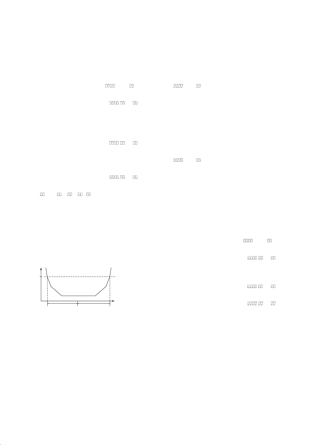
Note 1: The relation between the C1 error and focus bias is as shown in
Note 2: As the C1 error rate changes, perform the adjustment using the
the following figure. Find points a and b in the following figure
using the above adjustment. The focal point position C is
auto
matically calculated from points a and b.
average value.
C1 error
about 200
bc a
§
Focus bias
value
(F. BIAS)
Error Rate Check
CD Error Rate Check
Checking Method:
1. Load a check disc (MD) TDYS-1.
2. Rotate the [AMS] knob and display “CPLAY MODE”.
3. Press the [ENTER/YES] button twice and display “CPLAY
MID”.
4. “C1 = AD = ” is displayed.
5. Check that the C1 error rate is below 20.
6. Press the [EDIT/NO] button, stop playback, press the [EJECT]
§
button, and remove the check disc.
MO Error Rate Check
Checking Method:
1. Load a continuously recorded disc (Refer to “Page 15 Creating Continuously Recorded Disc”).
2. Rotate the [AMS] knob and display “CPLAY MODE”.
3. Press the [ENTER/YES] button twice and display “CPLAY
MID”.
4. “C1 = AD = ” is displayed.
5. If the C1 error rate is below 50, check that ADER is 00.
6. Press the [EDIT/NO] button, stop playback, press the [EJECT]
§
button, and remove the continuously recorded disc.
Focus Bias Check
Change the focus bias and check the focus tolerance amount.
Checking Method:
1. Load a continuously recorded disc (Refer to “Page 15 Creating Continuously Recorded Disc”).
2. Rotate the
3. Press the [ENTER/YES] button twice and display “CPLAY
MID”.
4. Press the [EDIT/NO] button when “C1 = AD = ” is
displayed.
5. Rotate the [AMS] knob and display “FBIAS CHECK”.
6. Press the [ENTER/YES] button and display “ / c = ”.
The first four digits indicate the C1 error rate, the two digits
after [/] indicate ADER, and the 2 digits after [c =] indicate
the focus bias value.
Check that the C1 error is below 50 and ADER is 00.
7. Press the [ENTER/YES] button and display “ / b = ”.
Check that the C1 error is not below about 200 and ADER is
not above 00 every time.
8. Press the [ENTER/YES] button and display “ / a = ”.
Check that the C1 error is not below about 200 and ADER is
not above 00 every time.
9. Press the [EDIT/NO] button, next press the [EJECT] button,
and remove the continuously recorded disc.
[AMS] knob and display “CPLAY MODE”.
§
Note 1: If the C1 error and ADER are above 00 at points a or b, the focus
bias adjustment may not have been carried out properly. Adjust
perform the beginning again.
– 18 –
Adjusting Points and Connecting Points
[BD Board] (Side A)
D101
[BD Board] (Side B)
IC171
TP58
(IOP)
RV101
TP57
(I + 5V)
TP31
(VC)
RV102
IC191
IC101
TP75
(TEO)
IC121
– 19 –
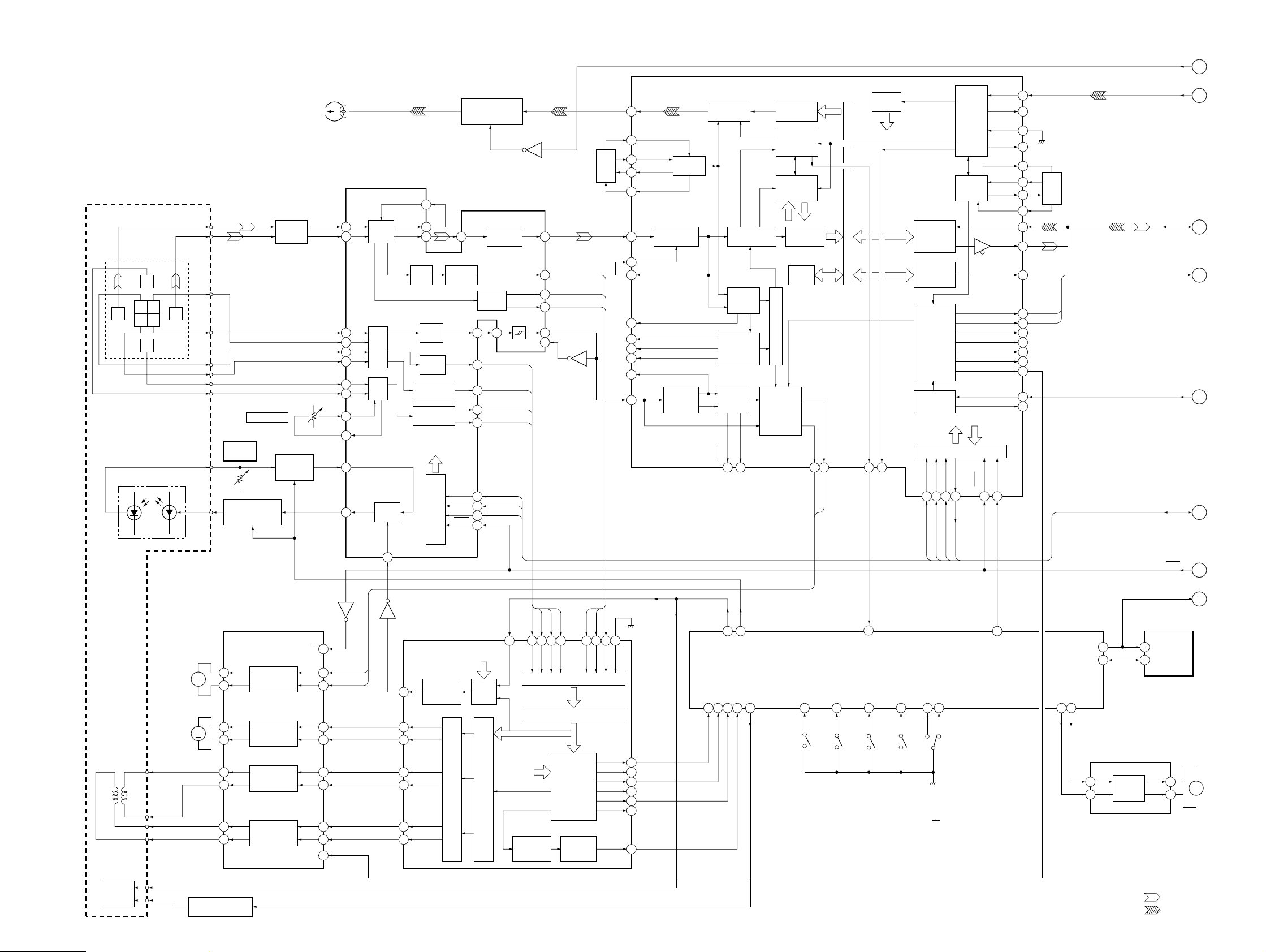
6-1. BLOCK DIAGRAM – SERVO Section –
F
C
I
DA
E
OPTICAL PICK-UP
(KMS-210A/J-N)
LASER DIODE
PD
B
DETECTOR
I
J
B
J
A
C
D
E
F
RV102
LASER
POWER
PD
ILCC
LD
AUTOMATIC
POWER CONTROL
Q162, 163
RV101
E-F BALANCE
I-V AMP
IC172
LASER ON
SWITCH
Q101
SECTION 6
DIAGRAMS
HR901
OVER WRITE HEAD
RF AMP, FOCUS/TRACKING
ERROR AMP
I
47
J
48
A
2 30
B
C
AMP
4
D
5
E
6
F
AMP
7
FI
8
FO
9
PD
10
AAPC
14
IC101
RF
AMP
I-V
I-V
APC
APCREF
11
OVER WRITE
HEAD DRIVE
IC181, Q181, 182
4
2
IC182
MORFI
45
MORFO
46
RFO
44 41 58
B.P.F.
AT
AMP
ABCD
AMP
FOCUS
ERROR AMP
TRACKING
ERROR AMP
SERIAL TO PARALLEL
43
AUX
SWITCH
ADFM
ABCD
SWDT
SCLK
XLAT
DECODER
XRST
AGCI
37
FE
35
TE
26
SE
29
18
19
20
17
RF
AGC & EQ
PEAK &
BOTTOM
ADIN
31 33
AUX
PEAK
BOTM
TLB
RF
34
39
38
ADFG
273
4
IC102
MDS-DRE1
SCTX
DIGITAL SIGNAL PROCESSOR,
EFM/ACIRC ENCODER/DECODER
IC121 (1/2)
EFMO
45
FILI
62
CLTV
60
PCO
61
FILTER
FILO
63
RFI
ASYI
56
ASYO
55
XPLCK
44
WFCK
41
GTOP
42
GFS
2
43
FMCK
22
ADFG
82
34MHz
PLL
COMPARATOR
ADIP
DEMODU-
LATOR
EFM
MODULATOR
EFM
DEMODULATOR
EFM
DIGITAL
PLL
EFM-SYNC
DETECTOR/
PROTECTOR
ADIP
DECODER
ADSY
ATER
23 13 93 94 14 15
REGISTER
SUBCODE
P TO W
PROCESSOR
SUBCODE Q
READER/
GENERATOR
REGISTER
32K
RAM
TIMING GENERATOR
DIGITAL
CLV
PROCESSOR
SPRD
SPFD
PEAK
DETECT
INTERNAL BUS
SQSY
DQSY
DIGITAL
AUDIO
IN/OUT
DIN PLL
(22MHz)
AUDIO
DATA
CONTROL
ECC
ENCODER/
DECODER
TIMING
GENERATOR
CLOCK
GENERATOR
CPU INTERFACE
SWDT
SCLK
XLAT
SRDT
8 9 10 11 16 24
XRST
DODT
DIDT
DOUT
DIFO
DICV
DIPD
C2PO
LRCK
MCLK
XBCK
WDCK
RFCK
XTAI
XTAO
REC
DIN
DIFI
DTI
DTO
BCK
FS4
27
28
21
20
53
51
49
52
29
30
31
33
32
36
37
39
40
90
35
34
FILTER
SWDT, SCLK, XLAT, SRDT
DODT
DATA
BCK, LRCK, C2PO
512FS
XRST
A
B
C
D
E
F
G
(Page 23)
(Page 23)
(Page 23)
(Page 23)
(Page 24)
(Page 23)
(Page 24)
4
SPINDLE/SLED MOTOR DRIVE,
FOCUS/TRACKING COIL DRIVE
IC151
FO4
M102
(SPINDLE)
M101
(SLED)
2-AXIS
DEVICE
(FOCUS)
HF
MODULE
05
TRK+
(TRACKING)
TRK–
FCS+
FCS–
WRPWR
MOD
22
M
M
HF MODULE SWITCH
Q164
RO4
24
FO2
15
RO2
13
FO3
29
RO3
26
FO1
8
RO1
11
SPINDLE
MOTOR DRIVE
SLED
MOTOR DRIVE
TRACKING
COIL DRIVE
FOCUS
COIL DRIVE
RI4
F/R4
RI2
RI3
RI1
CLK
Q151
33
OE
SPFD
19
SPRD
20
FI2
17
18
FI3
31
32
FI1
6
5
3
IC122
2
DIGITAL SERVO SIGNAL
LDDR
APC PWM
84
GENERATOR
SFDR
92
SRDR
91
TFDR
86
TRDR
85
FFDR
87
FRDR
89
PROCESSOR
IC121 (2/2)
PWM GENERATOR
APC
COMP./
FILTER
SERVO
SIGNAL PROCESSOR
676 7677 66 64 65 68 78
FE
TE
SE
WRPWR
SERVO
SEQUENCER
AUTO
ABCD
ANALOG MUX
A/D CONVERTER
OFTRK/
DFCT/FOK/
COUT/SHCK/
FS256
PROCESSOR
CONTROL
SENS
PEAK
BOTM
AUX1
OFTRK
DFCT
FOK
COUT
SHCK
FS256
SENS
AUX2
PLAY SW
S192
S192
(PACK OUT)
5
SYSTEM CONTROLLER
SQSY
OUT SW
57
LOW REFELECT RATE/
IC101 (1/4)
REC SW
59
S193
S193
(REC POSITION)
(REFLECT/PROTECT DETECT)
UN-PROTECT
PROTECT
REFLECT
77 78
S102
S102
HIGH REFELECT RATE/
WRITE PROTECT
71
79
LD-ON
WPOWER
FG
FOK
SENSE
SHOCK
68 69 70 76 66
MOD
98
3
2
99
4
1
12
LIMIT-IN
80 58
S101
(LIMIT)
S191
(PLAY POSITION)
S191
65
REC/PB
LOAD OUT
61 60
75
SCL
SDA
74
LOAD IN
LOADING MOTOR DRIVE
IN1
9
IN2
10
IC901
MOTOR
DRIVE
SCL
SCL
6
SDA
5
EEPROM
IC171
OUT1
4
OUT2
2
• SIGNAL PATH
: PLAY
: REC
H
M
(Page 23)
M191
(LOADING)
– 21 – – 22 –
MDS-DRE1
6-2. BLOCK DIAGRAM – MAIN Section (1/2) –
B
(Page 22)
C
(Page 22)
D
(Page 22)
A
(Page 22)
F
(Page 22)
I
(Page 25)
H
(Page 22)
X101
10MHz
DODT
DATA
BCK, LRCK,
C2PO
SCTX
SWDT, SCLK,
XLAT, SRDT
SWDT, SCLK,
XLAT, SRDT
SCL
13
15
6 5
3
DODT SELECTOR
IC153 (1/2)
SERIAL DATA
SELECTOR
IC154
3 4
2 1
53
52
XOUT
DSEL
XIN
DODT-SEL
4
2
IC151
(1/4)
1
2
1
5
IC151
8
(2/4)
9
13
95
93
BCK
91
LRCK
90
C2PO
92
12
D0 – D3
69, 68, 70, 71
2, 3, 22, 23
DQ1 – DQ4 A0 – A11
67
SCTX
DODT
95
DATA
93
BCK
LRCK
C2PO
69, 68, 70, 71
2, 3, 22, 23
DQ1 – DQ4 A0 – A11
DODT
DATA
BCK
LRCK
C2PO
TX
GENERATOR
55 – 52, 56 – 60, 65, 49, 48
8 – 11, 14 – 19, 7, 6
D-RAM
IC602
91
90
92
12
D0 – D3
INTERFACE
EFM DECODER
ADDRESS
A00 – A11
XLAT
SCLK
SWDT
39
33
31
SCLK
SWDT
XLAT-DEC
BCK
LRCK
C2PO
TX
40
INTERFACE
EFM ENCODER
ADDRESS
GENERATOR
55 – 52, 56 – 60, 65, 49, 48
8 – 11, 14 – 19, 7, 6
D-RAM
IC502
CD-ROM DECODER
XWE
67 66 62 61 2 3 4 9 17
4 5 21 20
XLAT-ENC
CD-ROM ENCODER
A00 – A11
40
34
F86
EXE
INTERFACE
ATRAC DECODER
RAM R/W CONTROLLER
MEMORY
DECODER
CPU INTERFACE
XRAS
XCAS
XOE
SWDT
SWDT
XOE
XWE
XCAS
XRAS
XWE
67 66 62 61 2 3 4 9 175 6
4 5 21 20
XWE
DATA
ATRAC
SCK
SCLK
40
34
F86
EXE
INTERFACE
ATRAC ENCODER
RAM R/W CONTROLLER
XRAS
XCAS
XOE
XOE
XCAS
XRAS
SHOCK PROOF MEMORY CONTROLLER,
MEMORY
INTERFACE
CONTROLLER
SENSE
XLAT
XLAT
XINT
SRDT
5 6
SRDT
SYSTEM CONTROLLER
SHOCK PROOF MEMORY CONTROLLER,
MEMORY
CONTROLLER
DATA
MEMORY
ATRAC
ENCODER
CPU INTERFACE
SWDT
SCK
XLAT
SRDT
SCLK
SWDT
ATRAC DECODER
IC601
CLOCK
GENERATOR
XRST
2
5 6
SRDT
IC101 (2/4)
INTERFACE
SENSE
XINT
AUDIO
INTERFACE
SPO
87
IC152
ATRAC ENCODER
IC501
CLOCK
GENERATOR
SPO
XRST
87
DIDT
94
DIN
42
DOUT
41
ABCK
43
ALRCK
44
OSCI
37
OSCO
36
90.3168MHz
SRDT SELECTOR
3
1
4
6
IC151 (3/4)
AUDIO
INTERFACE
X601
IC152
DIDT
DOUT
ABCK
ALRCK
OSCO
5
85
DIN
OSCI
32
SRDT
SRDT-SEL
94
42
41
43
LRCK
44
37
36
X501
45.1584MHz
23 24 47
XINT-DEC
BCK
XINT-ENC
BCK
RST-37
LRCK
COUNTER
IC253 – 255
LRCK
8
BCK
11
73
75
57
51
55
CLK
GPIO3
GPIO1
SDI0
SCKR
WSR
IC271
(1/2)
IC271
(2/2)
DSP
IC701
SCL
72 81 56 41
PARALLEL
DATA
10
9
13
12
EXTAL
GPIO2
SDO1
SDO2
SDO0
SCKT
WST
SDA
GPIO0
RVS
SDA-CDSP
SHIFT REGISTER
9
FLIP-FLOP
IC202 (1/2)
27
74
46
45
47
49
50
SDI1
RESET
36
RPD0
RST-DSP
& LATCH
IC256, 257
11
BCK
BCK
LRCK
MD0 – MD3
71, 69 – 67
1, 2, 18, 19
DQ1 – DQ4
LATCH
BCK
SDO1 (DATA)
SDO2 (ENABLE)
12
IC201
(1/4)
34
SAMPLING RATE CONVERTER
FS128
1
3
2
7
IC751
DATAI
BCKI
INPUT
LRCKI
FSI28
INTERFACE
MA00 – MA09
25 – 22, 20 – 18, 16, 14, 13
6 – 9, 11 – 15, 5
D-RAM
IC702
SAMPLING
CONVERTER
ATT/MODE
CONTROL
SWDT
42 41
SWDT
A0 – A9
BCK
RATE
SCK
SCLK
FS128
XLAT
40
XLAT
LRCK
COUNTER
IC259, 260
OUTPUT
INTERFACE
FRAME
COUNTER
INIT
10
MWR
7826 35 76 56
79 80
3 4 17
WE
VCO
OUT
3
IC201
(2/4)
563 5
2
1
IC201
(3/4)
DATAO
30
BCKO
31
LRCKO
32
XI
13
MRAS
MCAS
CAS
RAS
VCO
1/2
DIVIDER
VCO
IC251 (1/2)
DIVIDER
IC202 (1/2)
BCK
LRCK
86
87
88
SWDT
3
SCLK
4
SRDT
7
5
43 44 45
LAT-KEY
VCO
SI
BCK
LRCK
RVDT
SCK
TRDT
XLAT
IN
CONTROL
13
OSC
IC201 (4/4)
8
33
XTLI
KEY
IC801
XRST
10
WAVE
SHAPER
IC252
SO
REDY
XWO
(Page 25)
DIDT
J
SDTO
K
(Page 25)
PFD
PLL
IC251 (2/2)
LATCH
IC258
LRCK
LINE OUT
SELECTOR
IC153 (2/2)
4
FINB
5
FINA
4
(Page 25)
MCLK
L
BCK, LRCK
8
M
(Page 25)
SDTI
N
(Page 25)
13
XRST
G
(Page 22)
XRST
O
(Page 25)
512FS
E
(Page 22)
512FS
P
(Page 25)
PFD
OUT
612
9
10
12
6
8
12 11
IC151
(4/4)
3
• SIGNAL PATH
: PLAY
: REC (ANALOG IN)
: REC (DIGITAL IN)
54
48
AOUT-SEL
RST-DIG
XWO-KEY
READY-KEY
05
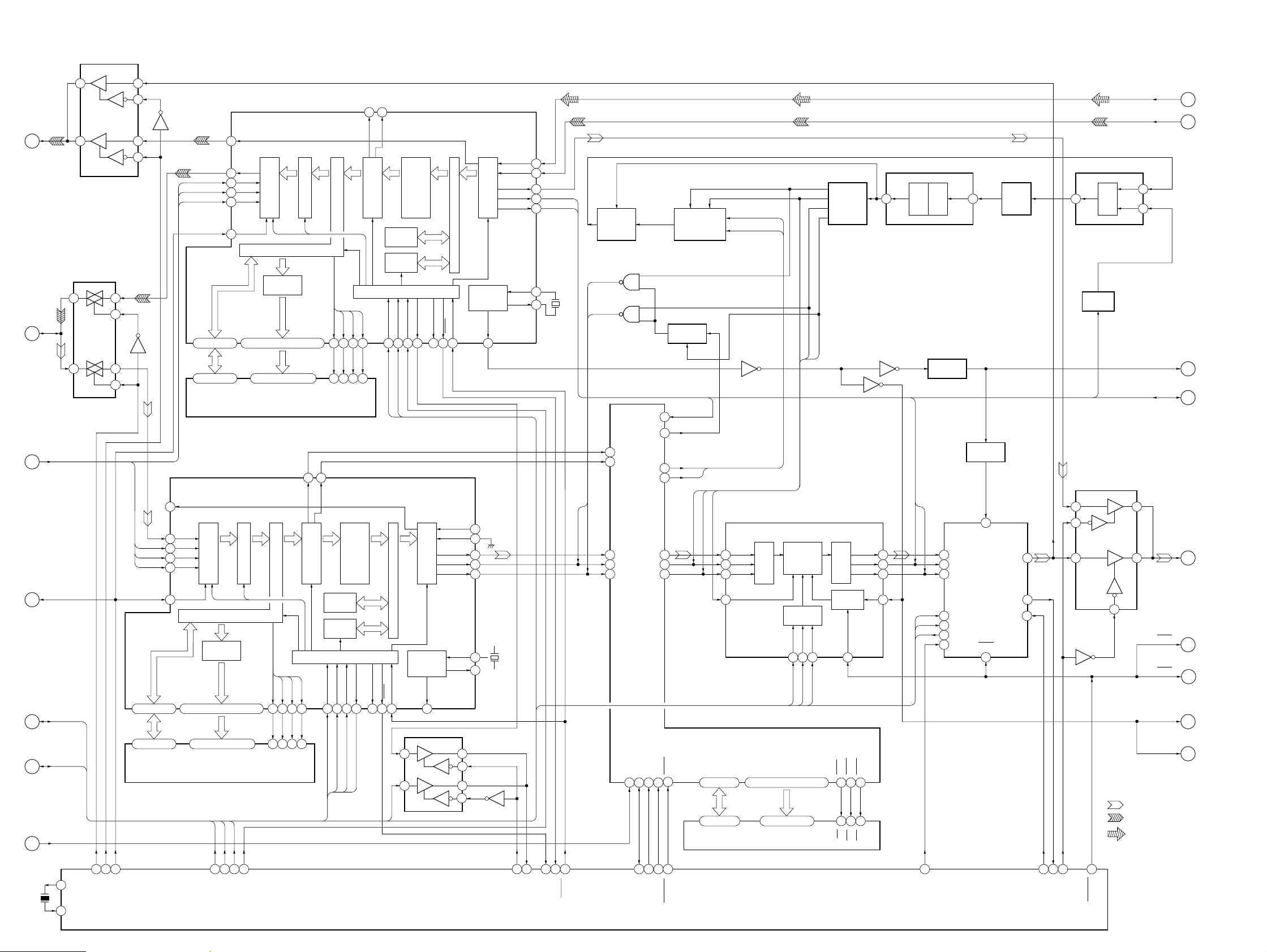
6-3. BLOCK DIAGRAM – MAIN Section (2/2) –
MDS-DRE1
(Page 24)
(Page 24)
(Page 23)
(Page 24)
(Page 24)
(Page 24)
(Page 24)
(Page 24)
(Page 27)
J
P
I
O
M
K
N
L
Q
DIDT
512FS
SWDT, SCLK,
XLAT, SRDT
XRST
BCK, LRCK
SDTO
SDTI
MCLK
POWER DOWN
SAMPLING RATE CONVERTER
DATAO
30
BCK
LRCK
BCKO
31
LRCKO
32
XI
13
SDTO
14
SDTI
13
MCLK
15
IC451
OUTPUT
INTERFACE
FRAME
COUNTER
INIT
10
BCK
LRCK
11
12
SCLK
LRCK
SERIAL I/O
INTERFACE
CLOCK
DIVIDER
SAMPLING
RATE
CONVERTER
ATT/MODE
CONTROL
SWDT
SCK
42 41 40
SCLK
SWDT
24
23
PWAD
PWDA
DECIMATION
INTER-
POLATOR
XLAT
XLAT
FILTER
DEM0
16
DATAI
BCKI
INPUT
INTERFACE
LRCKI
FI128
A/D, D/A CONVERTER
IC301
Σ∆
MODULATOR
Σ∆
MODULATOR
1
3
2
7
LOW-PASS
FILTER
INTERFACE RECEIVER
DATA OUT
23
BCKO
21
LRCKO
22
FS128
20
AINL+
5
AINL–
6
AOUTL
26
AOUTR
27
DIGITAL AUDIO
IC401
TIMING
PLL
AVOCKLRCK
11
R-CH
DEMODULATOR
LOCK ERROR
AOUTL+
10
9
AOUTL–
BUFFER
IC342 (1/2)
DATA
DETECT
ERROR
24
BUFFER
IC311
INPUT
INTERFACE
CPU INTERFACE
DQSY
SCK
SWDT
18
16
14
15
SCLK
SWDT
INL–
4
LOW-PASS
FILTER
IC342 (2/2)
MUTING
CONTROL SWITCH
Q101
D101
XLAT
SRDT
17
XLAT
SRDT
MUTING
Q352
R-CH
DIN1
DIN2
XMODE
10
LINE AMP
IC701
1
2
HEADPHONE
AMP
IC751
RV701
REC VOL
WAVE
SHAPER
IC602
R-CH
RV751
PHONE
LEVEL
R-CH
R-CH
J701
OPTICAL
RECEIVER
IC601
L
R
L
R
J601
COAXIAL IN
OPTICAL IN
IN
OUT
J751
PHONES
IC601
LINE
(ANALOG)
DIGITAL
42
05
DEEMP-ADA
49
AMUTE
SYSTEM CONTROLLER
IC101 (3/4)
50
19
ERROR
DQSY
• SIGNAL PATH
: PLAY
: REC (ANALOG IN)
: REC (COAXIAL DIGITAL IN)
: REC (OPTICAL DIGITAL IN)
– 25 –
– 26 –
MDS-DRE1
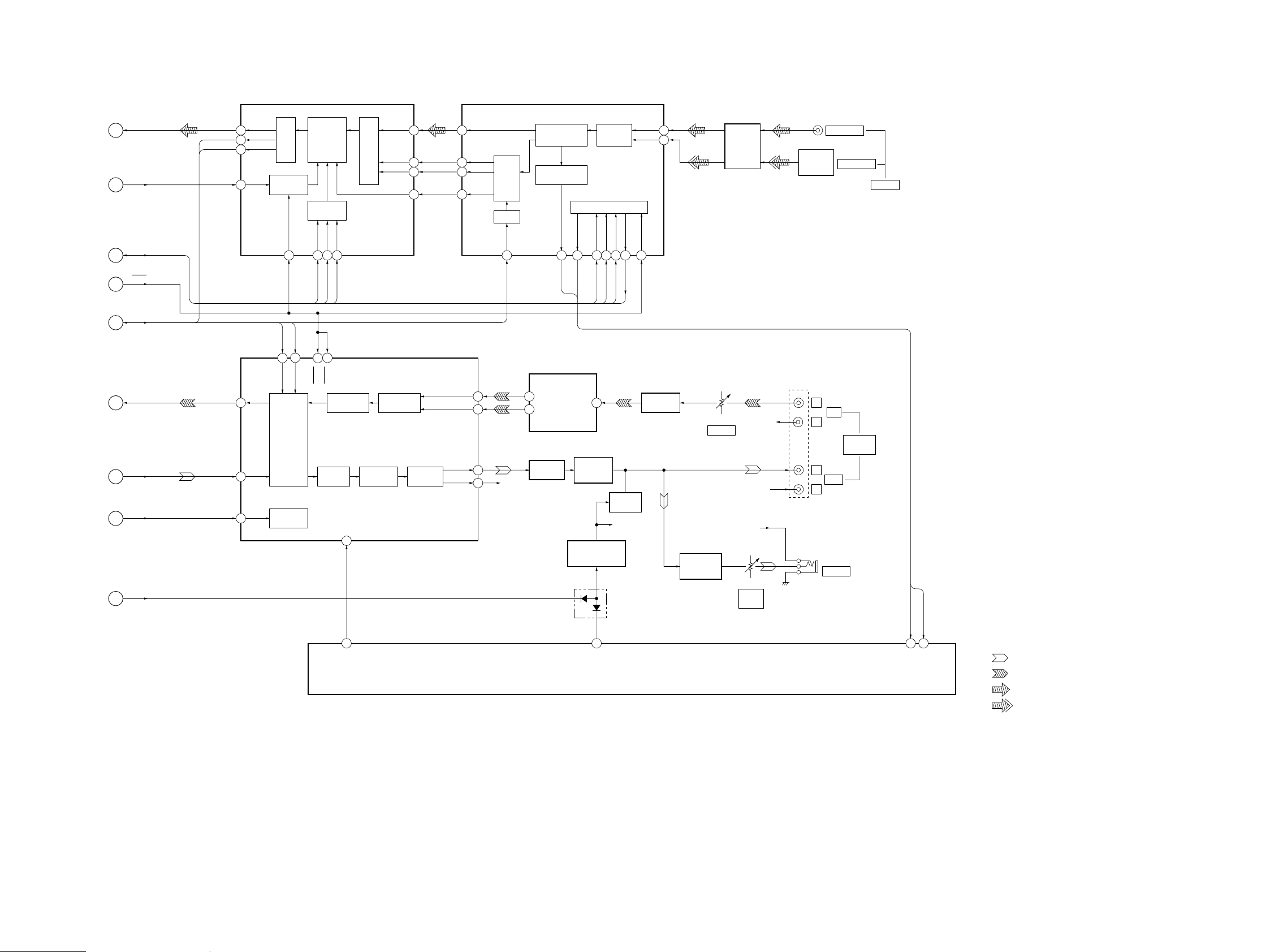
6-4. BLOCK DIAGRAM – DISPLAY/KEY/POWER SUPPLY Section –
FL DRIVER CONTROL,
KEY CONTROL, LED DRIVE
REC/PAUSE
PLAY/PAUSE
S305
≠ AMS ±
PUSH ENTER
J851
FOOT SW
JOG DIAL
DETECT SENSOR
PH381, 382
ROTARY
ENCODER
2
1
24
23
A
1
B
3
54
25
26
FSW1
FSW0
JOG0
JOG1
JOGA
JOGB
IC201
SWDT
SCLK
FLCS
FL-RES
RESET
31
33
34
46
D102
12
16
15
14
13
D101
FL DRIVER
IC101
SDATA
SCK
CS
RST
XIN
21 20
OSC
C107, R101
D1 – D16S1 – S36
12 – 1, 64 – 6159 – 33, 31 – 23
XOUT
FLUORESCENT
INDICATOR TUBE
FL101
(Page 25)
Q
POWER DOWN
+5V
MD SERVO SECTION B+
HEAD/PWM +5V
+5V
REGULATOR
IC191
10
6
DIG +5V
+5V/+7V REGULATOR
IC411
OUT 7V
OUT 5V
5V ON/OFF
+5V
REGULATOR
IC421
7V ON/OFF
21
VCC
REGULATOR
7
+10V
IC422
RECT
D205, 206
S301 – 304, 306,
S311 – 316, 361 – 365,
S371 – 376
PAD UNIT
LED DRIVE
IC421, 431
RV392
PITCH
RV391
SPEED
89 – 9465, 67, 69, 71, 73, 75, 77, 79
KEY6, KEY7
KEY0 – KEY3,
LED-R.PAUSE
LED1-O – LED8-O
66, 68, 70, 72, 74, 76, 78, 80
INPUT-SEL0
INPUT-SEL1
LED1-G – LED8-G
KEY-CONT
97
SPEED-CONT
95
DTCK
DTIN
DTOUT
DTIN
DTCK
DTOUT
RTS
PMCU-REF
35 36 37 38 20
36 353738 34
LED-PP
LED-CUE
XIN
XOUT
DTCS
DTCS
POWER DOWN
LDDRV +7V
LOADING MOTOR
DRIVE (IC901) B+
SYS +5V
MCU +5V
(IC101) B+
DETECT
IC431
+5V
A/D, D/A CONVERTER
(IC301) B+
D451
D453
BT451
LITHIUM
BATTERY
D431
INI
2
3
RST
OUT 7V
10
OUT 5V
6
FL DRIVER (IC101) B–
+5V
REGULATOR
IC302
DRIVE
D364 – 366
PLAY/PAUSE
D361 – 363
CUE
D371
REC PAUSE
M801
M
(FAN)
SYSTEM CONTROLLER
IC101 (4/4)
7
PDOWN
SYSTEM CONTROLLER
12
51
STB
RESET
LED DRIVE
30
29
28
88
87
15
13
Q363, 364
LED DRIVE
Q361, 362
LED DRIVE
S601
INPUT
X201
10MHz
Q371
ANLG
COAX
OPT
FAN MOTOR
Q801, 802
87
FAN CONT
D432
RESET SIGNAL
GENERATOR
IC451
+5V/+7V REGULATOR
IC401
5V ON/OFF
7V ON/OFF
1
2
–32V
HEADPHONE
AMP (IC751)
A+6V
A–6V
REGULATOR
REGULATOR
+6V
IC301
–6V
IC302
VCC
VCC
5
7
–32V
REGULATOR
IC501
B+
B–
RECT
D207, 208
RECT
D210, 211
RECT
D209
RECT
D201 – 204
TO FL101
T901
POWER
TRANSFORMER
S801
U
(POWER)
NOISE
FILTER
AC
AC
~ AC IN
05
– 27 –
– 28 –
MDS-DRE1
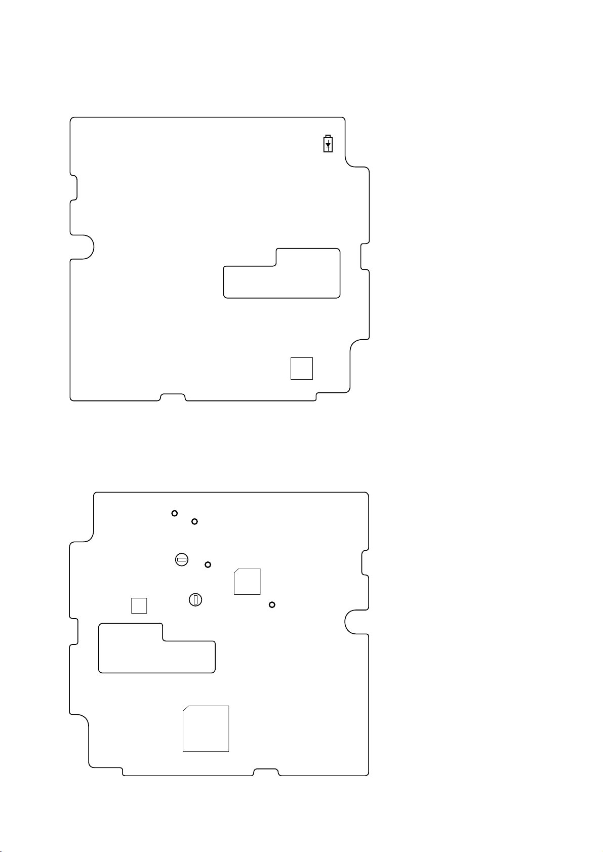
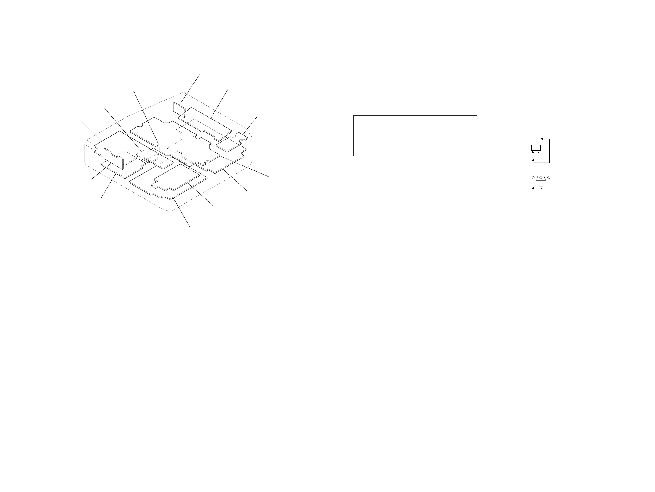
• Circuit Boards Location
MOTOR board
JOG board
EJECT board
BD board
DETECTION SW board
PSW board
FADER board
DIGITAL board
DISPLAY board
POWER board
REC board
CENTER board
6-5. NOTES FOR PRINTED WIRING BOARD AND SCHEMATIC DIAGRAM
(In addition to this, the necessary note is printed in each block)
Note on Schematic Diagram:
• All capacitors are in µF unless otherwise noted. pF: µµF
50 WV or less are not indicated except for electrolytics
and tantalums.
• All resistors are in Ω and 1/
specified.
• % : indicates tolerance.
¢
•
• 2 : nonflammable resistor.
• C : panel designation.
• U : B+ Line.
• V : B– Line.
• H : adjustment for repair.
• Voltages and waveforms are dc with respect to ground
• Voltages are taken with a V OM (Input impedance 10 MΩ).
• Waveforms are taken with a oscilloscope.
• Circled numbers refer to waveforms.
• Signal path.
: internal component.
Note:
The components identified by mark ! or dotted
line with mark ! are critical for safety.
Replace only with part
number specified.
under no-signal conditions.
no mark : STOP
( ) : PLAY
〈〈 〉〉 : REC
Voltage variations may be noted due to normal production tolerances.
Voltage variations may be noted due to normal production tolerances.
E : PLAY
j : REC (ANALOG IN)
k : REC (DIGITAL IN)
f : REC (COAXIAL DIGITAL IN)
h : REC (OPTICAL DIGITAL IN)
: Impossible to measure
∗
4
W or less unless otherwise
Note:
Les composants identifiés par
une marque ! sont critiques
pour la sécurité.
Ne les remplacer que par une
piéce portant le numéro
spécifié.
Note on Printed Wiring Board:
• X : parts extracted from the component side.
• Y : parts extracted from the conductor side.
®
•
• b : Pattern from the side which enables seeing.
(The other layers' patterns are not indicated.)
Caution:
Pattern face side: Parts on the pattern face side seen from
(Side B) the pattern face are indicated.
Parts face side: Parts on the par ts face side seen from
(Side A) the parts face are indicated.
• Indication of transistor.
: Through hole.
C
Q
B
E
Q
B
CE
These are omitted.
These are omitted.
– 29 –
– 30 –
 Loading...