Sony KDL-52Z5500, KDL-46Z5500 Schematic

HISTORY
Model Name: KDL-40/46/52Z5500
SERVICE MANUAL
Click on Page Number to display details of change
Date Part Number Description of Revisions Version
2009.02 9-883-446-01 Original Manual 1.0
2009.09 9-883-446-02
Update Self Diagnosis Table and working hours
table (P.10)
2.0
SERVICE MANUAL
MODEL DEST
KDL-40Z5500 AEP / UK
KDL-46Z5500 AEP / UK
KDL-52Z5500 AEP / UK
EX2L-Paprika
CHASSIS
- 1 -
RM-ED019

TABLE OF CONTENTS
Section Title Page Section Title Page
1. GENERAL
Caution ............................................................... 3
Specifications ...................................................... 6
Connectors .......................................................... 8
Self Diagnosis ..................................................... 9
2. DISASSEMBLY
2-1. Rear Cover Removal ............................................. 11
2-2. Rear Cover Removal (40/46 inches) ..................... 11
2-3. Rear Cover Removal (52 inches) .......................... 11
2-4. Rear Cover Installation (40/46 inches) ................. 11
2-5. Rear Cover Installation (52 inches) ...................... 12
2-6. Stand Assy Removal ............................................. 12
2-7. Stay Top Removal .................................................. 12
2-8. Stay Top Installation .............................................. 12
2-9. Switch Unit Removal ............................................ 13
2-10. Loudspeaker Removal ......................................... 13
2-11. G6NS/G7NS Board Removal .............................. 13
2-12. D1N/D3N Board Removal .................................. 13
2-13. D2N/D4N Board Removal .................................. 14
2-14. BA Board Removal ............................................. 14
2-15. HL1A Board Removal ........................................ 14
2-16. HSN Board Removal ........................................... 14
3. SERVICE MENUS
3-1. How to enter the Service Mode .......................... 15
3-2. Changing TVM Data Settings ............................ 15
3-3. Writing TVM Data ............................................. 15
3-4. Trouble Shooting ................................................ 16
4. DIAGRAMS
4-1. Block Diagram ................................................... 19
4-2. Circuit Board Location ....................................... 20
4-3. Schematic Diagrams and Printed Wiring
Boards ................................................................. 20
BA Board Schematic Diagram ........................... 21
D1N Board Schematic Diagram (40/46 inches)
D2N Board Schematic Diagram (40/46 inches) 40
D3N Board Schematic Diagram (52 inches) ..... 41
39
D4N Board Schematic Diagram (52 inches) ..... 42
G6NS Board Schematic Diagram (40 inches) ... 43
HL1A Board Schematic Diagram ...................... 45
HSN Board Schematic Diagram ........................
BA Printed Wiring Board ................................... 46
HSN Printed Wiring Board
HL1A Printed Wiring Board ............................... 47
................................. 46
45
D1N Printed Wiring Board (40/46 inches) ......... 48
D2N Printed Wiring Board (40/46 inches) ......... 49
D3N Printed Wiring Board (52 inches) .............. 50
D4N Printed Wiring Board (52 inches) .............. 51
G6NS Printed Wiring Board (40 inches) ............ 52
5. EXPLODED VIEWS
5-1. Chassis ................................................................ 54
5-2. Front Cabinet Assy & Stand Assy ...................... 56
5-3. Rear Cover & Power Supply Cords .................... 57
6. ELECTRICAL PARTS LIST
...................................... 58
WARNING !!
AN ISOLATION TRANSFORMER SHOULD BE USED DURING ANY
SERVICE WORK TO AVOID POSSIBLE SHOCK HAZARD DUE TO
LIVE CHASSIS, THE CHASSIS OF THIS RECEIVER IS DIRECTLY
CONNECTED TO THE POWER LINE.
SAFETY-RELATED COMPONENT WARNING !!
COMPONENTS IDENTIFIED BY SHADING AND MARKED
THE EXPLODED VIEWS AND IN THE PARTS LIST ARE CRITICAL
FOR SAFE OPERATION. REPLACE THESE COMPONENTS WITH
SONY PARTS WHOSE PART NUMBERS APPEAR AS SHOWN IN
THIS MANUAL OR IN SUPPLEMENTS PUBLISHED BY SONY.
£ ON
- 2 -
Partnumber Diameter Remarks
7-640-005-19 0.3mm 0.25Kg
7-640-005-20 0.4mm 0.50Kg
7-640-005-21 0.5mm 0.50Kg
7-640-005-22 0.6mm 0.25Kg
7-640-005-23 0.8mm 1.00Kg
7-640-005-24 1.0mm 1.00Kg
7-640-005-25 1.2mm 1.00Kg
7-640-005-26 1.6mm 1.00Kg
SECTION 1 GENERAL
How to replace the fuse.
Open the fuse compartment with
a screwdriver blade and replace
the fuse.
FUSE
ASA
T
mark.
SECTION 1 GENERAL
CAUTION
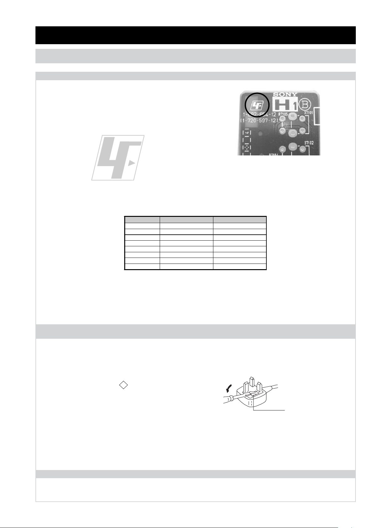
Lead Free Soldered Boards
example
The circuit boards used in these models have been processed using
Lead Free Solder. The boards are identified by the LF logo located
close to the board designation e.g. H1 etc [ see example ]. The
servicing of these boards requires special precautions to be taken as
outlined below.
Lead Free Solder material must be used to comply with environmental requirements of new solder joints. Lead Free Solder is available
under the following part numbers :
Due to the higher melting point of Lead Free Solder the soldering iron tip temperature needs to be set to 370 degrees centigrade. This
requires soldering equipment capable of accurate temperature control coupled with a good heat recovery characteristics.
For more information on the use of Lead Free Solder, please refer to http://www.sony-training.com
UK PLUG WARNING
WARNING (UK Models only)
The flexible mains lead is supplied connected to a B.S. 1363 fused
plug having a fuse of the correct rating for the set. Should the fuse
need to be replaced, use a fuse of the same rating approved by ASTA
to BS 1362, ie one that carries the
IF THE PLUG SUPPLIED WITH THIS APPLIANCE IS NOT SUITABLE
FOR THE OUTLET SOCKETS IN YOUR HOME, IT SHOULD BE CUT
OFF AND AN APPROPRIATE PLUG FITTED. THE PLUG SEVERED
FROM THE MAINS LEAD MUST BE DESTROYED AS A PLUG WITH
BARED WIRES IS DANGEROUS IF ENGAGED IN A LIVE SOCKET.
When an alternative type of plug is used, it should be fitted with the
correct rating fuse, otherwise the circuit should be protected by the
same rating fuse at the distribution board.
mark.
LCD PANEL CAUTION
Whilst working on this product, it is not recommended to lay the TV set face down when powered up, as this can result in panel problems.
If it is necessary to power up the TV set when face down, the time should be minimised as much as possible.
- 3 -
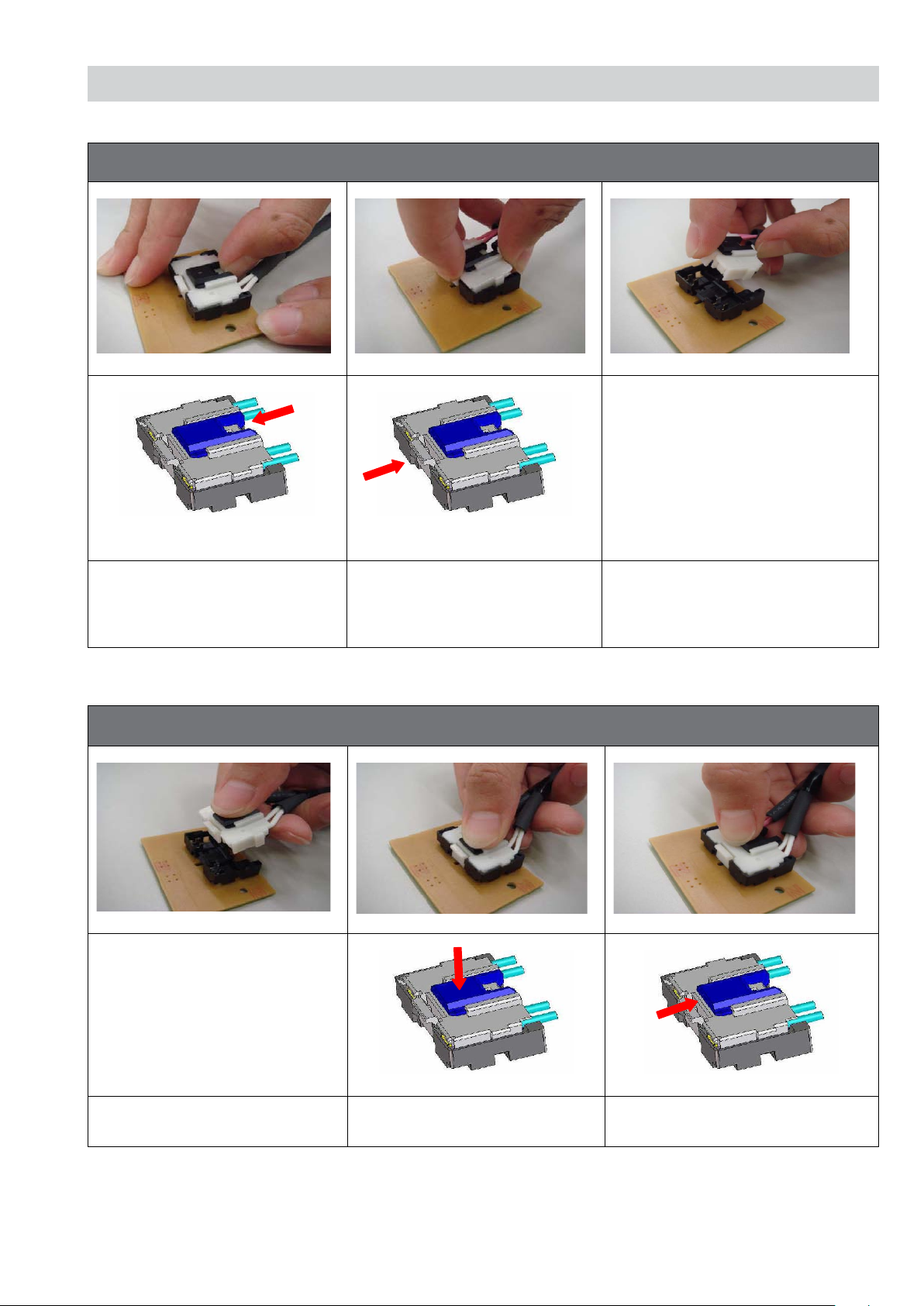
1. MDF-61 Connector (Removal)
CAUTION
Slide the slider to release slider
lock.
2. MDF-61 Connector (Refiitting)
Press the centre lock tab to
release the lock and pull the
connector up
Remove connector
Hold the centre of connector Press centre of connector to insert Slide the slider to lock connector
- 4 -
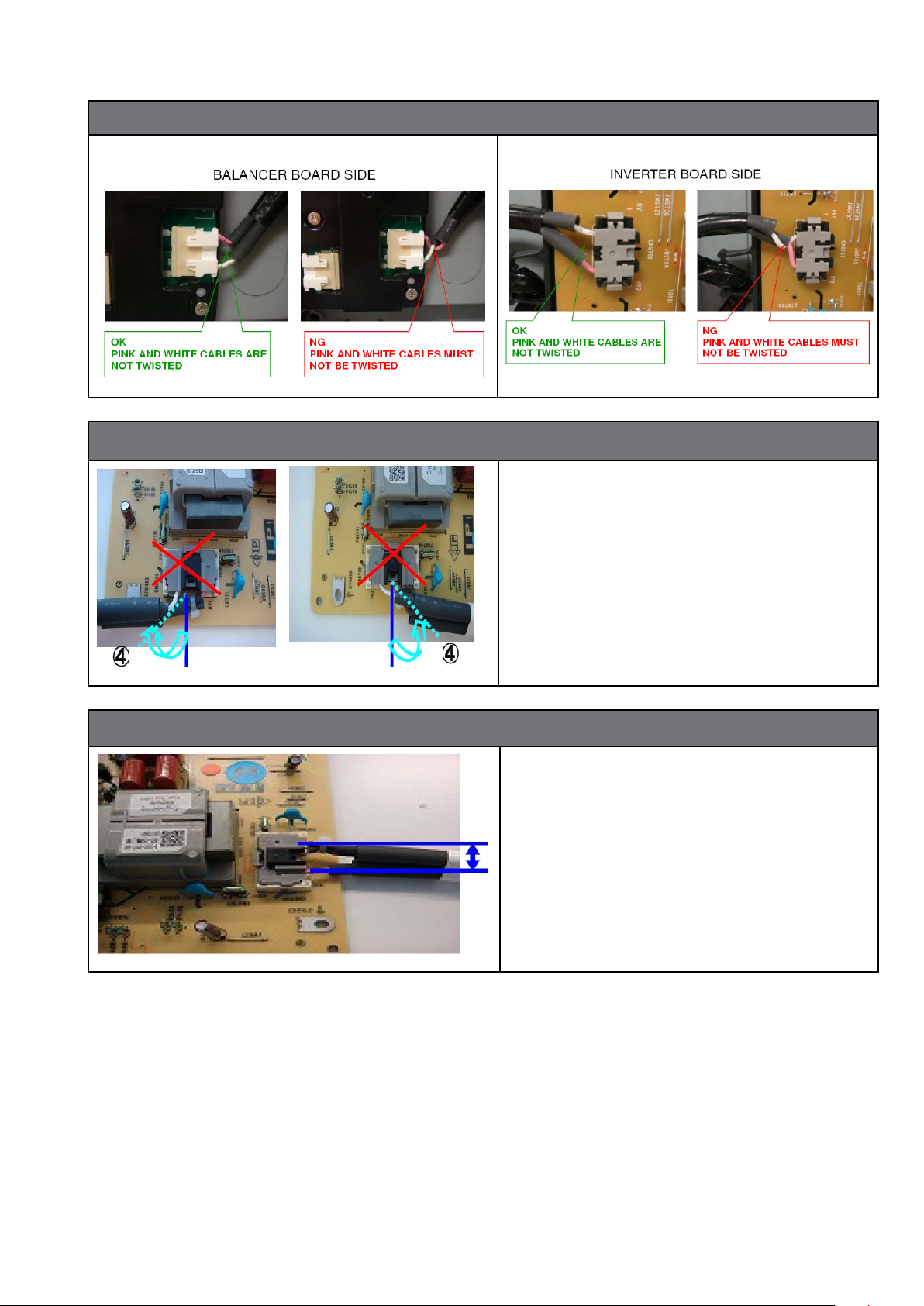
3. The harness must not be crossed or twisted
4. Wire Dressing at connector
The harness must not bend more
than 45 degrees from the direction of
the connector base to avoid crossing
or twisting.
5. Wire distance at connector
The distance between each wire must
be wider than 4mm to ensure isolation from lamp voltage.
- 5 -
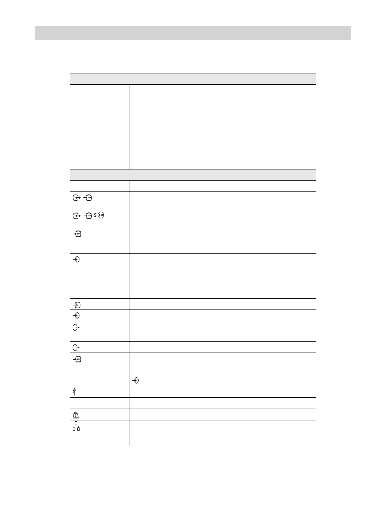
System
Panel system
LCD (Liquid Crystal Display) Panel
TV system
Analogue: Depending on your country/area selection: B/G/H, D/K, L, I
Digital: DVB-T/DVB-C
Colour/video system
Analogue: PAL, PAL60 (only video input), SECAM, NTSC3.58, NTSC4.43 (only video input)
Digital: MPEG-2 MP@ML/HL, H.264/MPEG-4 AVC MP/HP@L4
Channel coverage
Analogue: VHF: E2–E12/UHF: E21–E69/CATV: S1–S20/HYPER: S21–S41
D/K: R1–R12, R21–R69/L: F2–F10, B–Q, F21–F69/I: UHF B21–B69
Digital: VHF/UHF
Sound output
10 W + 10 W
Input/Output jacks
Aerial/Antenna cable
75 ohm external terminal for VHF/UHF
/ AV1
21-pin scart connector (CENELEC standard) including audio/video input, RGB input and TV audio/video
output.
/ / AV2
21-pin scart connector (CENELEC standard) including audio/video input, RGB input and selectable
audio/video output.
COMPONENT IN
Supported formats: 1080p, 1080i, 720p, 576p, 576i, 480p, 480i
Y: 1 Vp-p, 75 ohms, 0.3V negative sync/P
B/CB
: 0.7 Vp-p, 75 ohms/
P
R/CR
: 0.7 Vp-p, 75 ohms
COMPONENT IN
Audio input (phono jacks)
HDMI IN1, 2, 3, 4
Video: 1080/24p, 1080p, 1080i, 720p, 576p, 576i, 480p, 480i
Audio: Two channel linear PCM: 32, 44.1 and 48 kHz, 16, 20 and 24 bits, Dolby Digital
Analogue audio input (minijack) (HDMI IN1 only)
PC Input (Page 7)
AV3
Video input (phono jack)
AV3
Audio input (phono jacks)
DIGITAL AUDIO
OUT (OPTICAL)
Digital optical jack (Two channel linear PCM, Dolby Digital)
Audio output (phono jacks)
PC IN
PC Input (D-sub 15-pin) (Page 7)
G: 0.7 Vp-p, 75 ohms, non Sync on Green/B: 0.7 Vp-p, 75 ohms/
R: 0.7 Vp-p, 75 ohms/HD: 1-5 Vp-p/VD: 1-5 Vp-p
PC audio input (minijack)
USB port
i
Headphones jack
CAM (Conditional Access Module) slot
LAN
10BASE-T/100BASE-TX connector (Depending on the operating environment of the network, connection
speed may differ. 10BASE-T/100BASE-TX communication rate and communication quality are not
guaranteed for this TV.)
SPECIFICATIONS
- 6 -

*Specified standby power is reached after the TV finishes necessary internal processes.
Design and specifications are subject to change without notice.
Model name KDL-52Z5500 KDL-46Z5500 KDL-40Z5500 KDL-40Z5710
Power and others
Power requirements
220 V – 240 V AC, 50 Hz
Screen size (measured
diagonally)
52 inches/
Approx. 132.2 cm
46 inches/
Approx. 116.8 cm
40 inches/Approx. 101.6 cm
Display resolution
1,920 dots (horizontal) × 1,080 lines (vertical)
Power
consumption
in “Home”/
“Standard”
mode
194 W 166 W 154 W
in “Shop”/
“Vivid”
mode
330 W 241 W 210 W
Standby power
consumption*
0.19 W (16.5 W when “Quick Start” is set to “On”)
Model
name
KDL-52Z5500 KDL-46Z5500 KDL-40Z5500 KDL-40Z5710
Dimensions (Approx.) (w × h × d)
with
TableTop
Stand
124.0 × 82.1 × 35.8 cm 109.1 × 72.5 × 33.0 cm 95.8 × 64.9 × 30.3 cm 95.8 × 64.9 × 30.2 cm
without
TableTop
Stand
124.0 × 76.7 × 8.6 cm 109.1 × 67.2 × 8.6 cm 95.8 × 59.6 × 8.6 cm
Mass (Approx.)
with
TableTop
Stand
31.3 kg 25.3 kg 20.8 kg
without
TableTop
Stand
27.2 kg 21.9 kg 17.9 kg
PC input signal reference chart for PC and HDMI IN 1, 2, 3, 4
* 1080p timing when applied to the HDMI input will be treated as a video timing and not a PC timing. This
affects the “Video Settings” menu and “Screen” menu settings.
To view PC contents, set “Screen Format” to “Wide” and “Display Area” to “Full Pixel”.
~
• This TV’s PC input does not support Sync on Green or Composite Sync.
• This TV’s PC input does not support interlaced signals.
• For the best picture quality, it is recommended to use the signals in the above chart with a 60 Hz vertical
frequency (boldfaced).
Resolution
Horizontal
frequency (kHz)
Vertical
frequency (Hz)
Standard
Signals Horizontal
(Pixel)
× Vertical
(Line)
VGA
640 × 480 31.5 60 VESA
640 × 480 37.5 75 VESA
720 × 400 31.5 70 VESA
SVGA
800 × 600 37.9 60 VESA
800 × 600 46.9 75 VESA
XGA
1024 × 768 48.4 60 VESA
1024 × 768 56.5 70 VESA
1024 × 768 60.0 75 VESA
WXGA
1280 × 720 45.0 60 EIA
1280 × 768 47.4 60 VESA
1280 × 768 47.8 60 VESA
1280 × 960 60.0 60 VESA
1360 × 768 47.7 60 VESA
SXGA
1280 × 1024 64.0 60 VESA
HDTV
1920 × 1080 66.6 60 VESA*
1920 × 1080 67.5 60 EIA*
- 7 -
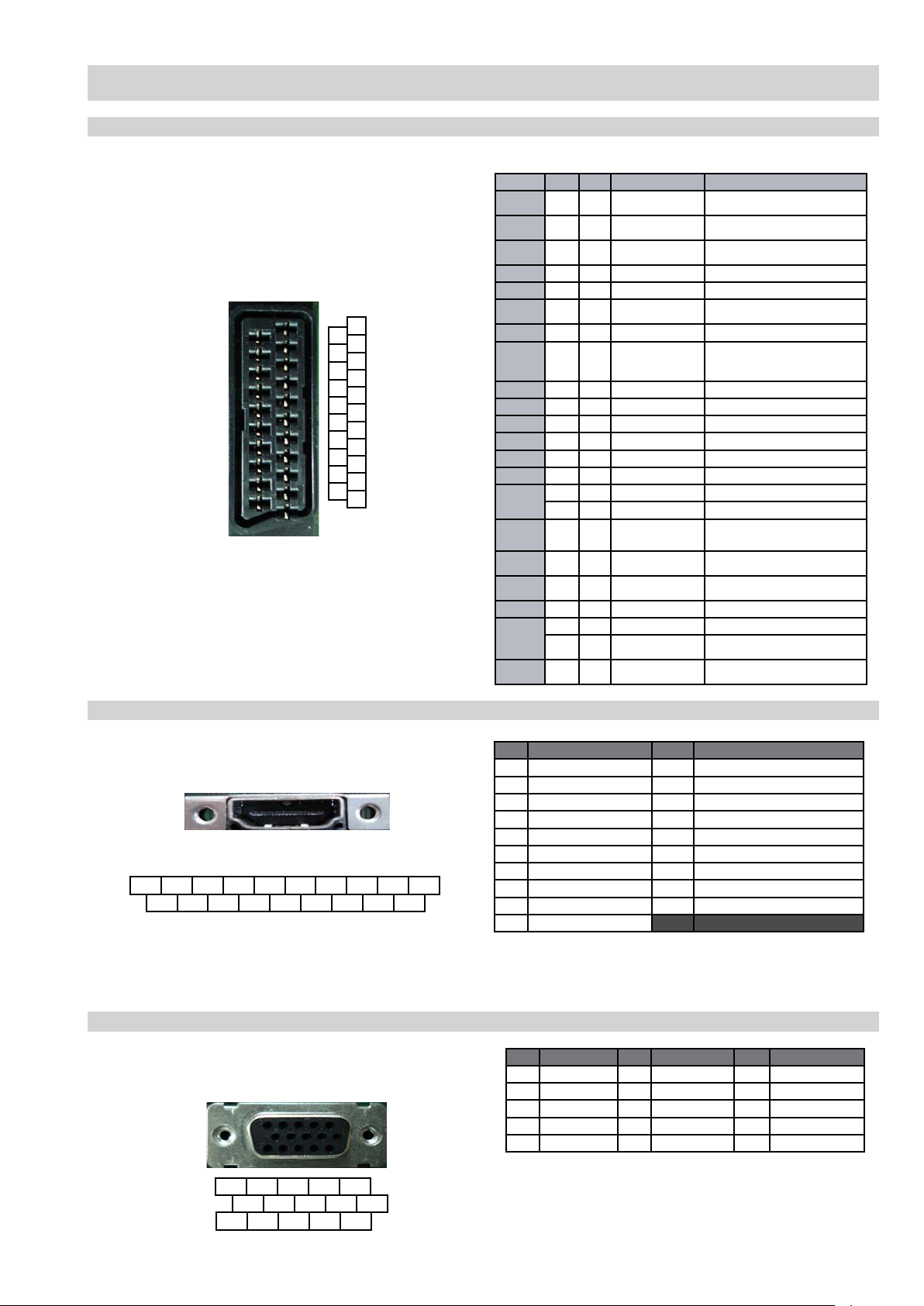
21 Pin Connector (SCART)
CONNECTORS
Pin No AV-1 AV-2 Signal Signal Level
1 • • Audio Output B
2 • • Audio Input B
3 • • Audio Output A
4 • • Ground (Audio)
5 • • Ground (Blue)
6 • • Audio Input A (Left) Standard Level: 0.5V rms
1
2
3
4
5
6
7
8
9
10
11
12
13
14
15
16
17
18
19
20
21
7 • • Blue Input 0.7V +/- 3dB, 75Ω, positive
8 • • Function Select
9 • • Ground (Green)
10 - • AV Link
11 • • Green Input 0.7V +/- 3dB, 75Ω, positive
12 - • Open
13 • • Ground (Red)
14 • • Ground (Blanking)
15
16 • • Blanking Input
17 • • Ground
18 • • Ground
19 • • Video Output 1V +/-3dB, positive sync 0.3V (-3+10dB)
20
21
• • Red Input 0.7V +/- 3dB, 75Ω, positive
• • S signal Chroma Input 0.3V +/-3dB, 75Ω, positive
• • Video Input 1V +/-3dB, positive sync 0.3V (-3+10dB)
• • Video Input Y
• • Common Ground
(Right)
(Right)
(Left)
(AV control)
(Y Signal)
(Video Output)
(Video Input)
(S Signal)
(Shield)
Standard Level: 0.5V rms
Impedance: less than 1KΩ*
Standard Level: 0.5V rms
Impedance: more than 10KΩ*
Standard Level: 0.5V rms
Impedance: less than 1KΩ*
Impedance: more than 10KΩ*
High State (9.5~12V): AV mode
Low State (0~2V): TV mode
Impedance: more than 10KΩ*
Capacitance: less than 2nF
High State (1~3V)
Low State (0~0.4V)
Impedance: 75Ω
1V +/-3dB, positive sync 0.3V (-3+10dB)
HDMI Connector
19 17 15 13 11 9 7 5 3 1
18 16 14 12 10 8 6 4 2
15 Pin D Sub Connector (PC)
Pin No Signal Assignment Pin No Signal Assignment
1 TMDS Data2+ 11 TDMS Clock Shield
2 TMDS Data2 Shield 12 TMDS Clock-
3 TMDS Data2- 13 CEC
4 TMDS Data1+ 14 Reserved (N.C. on device)
5 TMDS Data1 Shield 15 SCL
6 TMDS Data1- 16 SDA
7 TMDS Data0+ 17 DDC/CEC Ground
8 TMDS Data0 Shield 18 +5V power
9 TMDS Data0- 19 Hot Plug Detect
10 TMDS Clock+
Pin No Signal Assignment Pin No Signal Assignment Pin No Signal Assignment
1 Red Output 6 Red Return 11 Monitor IDO in display
2 Green Output 7 Green Return (Ground) 12 DCC Serial Data
3 Blue Output 8 Blue Return (Ground) 13 Horizontal Sync
4 Unused 9 +5V DC 14 Vertical Sync
5 Ground 10 Sync Return (Ground) 15 DCC Serial Clock
5 4 3 2 1
10 9 8 7 6
15 14 13 12 11
- 8 -

EX2L SELF DIAGNOSTIC SOFTWARE
erusaemretnuoCrorrEsemit gniknilB
2 DC_DET Replace either/both z Power board
(G6NS (40"), Power Unit (G7NS)
(46"/52")
z BA board
5 DC_ALERT Replace BA board.
6 BACKLIGHT Replace either/all z D1N(40"/46"), D2N(40"/46"),
D3N(52"), D4N(52")
z BA board
z
Panel
z Power Board
(G6NS (40"), Power Unit (G7NS)
(46"/52"))
7 INTERNAL TEMP Replace z BA board
A8 UDIO Replace either/all z Power board
(G6NS (40"), Power Unit (G7NS)
(46"/52")
z BA board
z Speaker
10 DIGITAL FE/DE Replace z BA board.
htob/rehtie ecalpeRHFR21 z Panel
z BA Board
13 BALANCER Replace either/all z BA board.
z Power board
G6NS (40"), Power Unit (G7NS)
(46"/52")
z D1N(40"/46"), D2N(40"/46"),
D3N(52"), D4N(52")
ecalpeRNOC-T41 z Panel.
z BA Board
The identification of errors within the EX2L chassis is triggered in one of two ways :- 1: Busy or 2: Device failure to respond to IIC. In the
event of one of these situations arising the software will first try to release the bus if busy (Failure to do so will report with a continuous flashing LED) and then communicate with each device in turn to establish if a device is faulty. If a device is found to be faulty the relevant device
number will be displayed through the LED (Series of flashes which must be counted).
LED Error Codes and Countermeasures
- 9 -
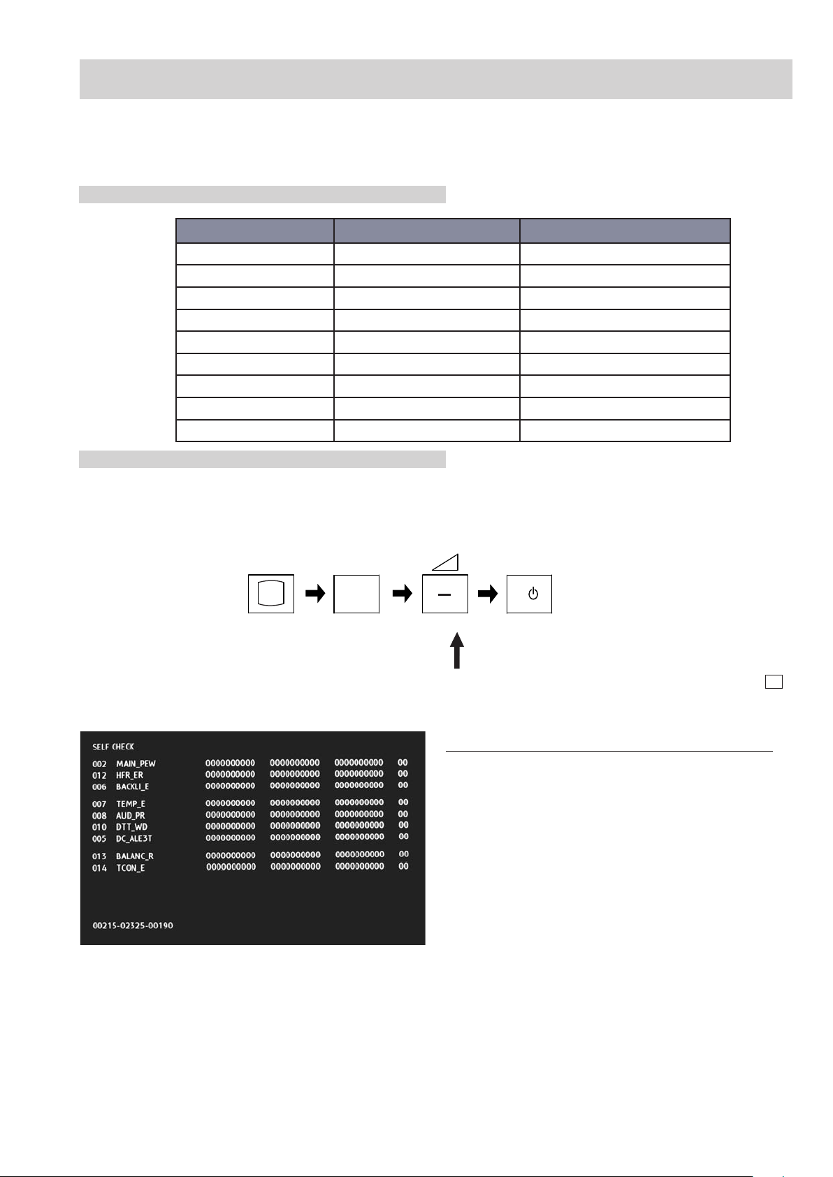
I/
TV
To bring up the self diagnostic screen display
i+
5
+
(ON SCREEN (DIGIT 5) (VOLUME +) (TV)
DISPLAY)
In standby mode, press the following buttons on the remote commander sequentially in rapid sucession as shown below:
Note that this differs from entering the service mode (Volume + )
(TV STANDBY)
(ON SCREEN
DISPLAY)
(DIGIT 5)
(VOLUME -)
The following menu appears as shown below:
Ver 2.0
EX2L SELF DIAGNOSTIC SOFTWARE
The identification of errors within the EX2L chassis is triggered in one of two ways :- 1: Busy or 2: Device failure to respond to IIC. In the
event of one of these situations arising the software will first try to release the bus if busy (Failure to do so will report with a continuous flashing LED) and then communicate with each device in turn to establish if a device is faulty. If a device is found to be faulty the relevant device
number will be displayed through the LED (Series of flashes which must be counted).
LED Error Codes and Descriptions
LED Flashes Error Description Error (Comp ref)
02 main Power Error Pwr_Err
05 DC_Alert3 DC_Alt
06 Backlight Error Bck_Lgt
07 Thermal Error Thm_Err
08 Audio Error Aud_Err
10 Digital FE/BE Error Dig_Err
12
13 Balancer Error Bal_Err
14 T-Con Error Tcn_Err
HFr Error (T-Con) Hfr_Err
Self Diagnostic Screen Display
WorkIng TImE (BoTTom LEFT CornEr)
xxxxx-yyyyy-zzzzzz(e.g. 00215-02325-00190)
1. xxxxx = Total operation time
Working time Stby+ Power on
2. yyyyy = Boot count
Power on / off / Stby operations
3. zzzzz = Working Hours (Panel)
Panel working time (backlight is on)
To exit the “Self Diagnostic Screen Display” please turn the TV set off and then on again.
- 10 -
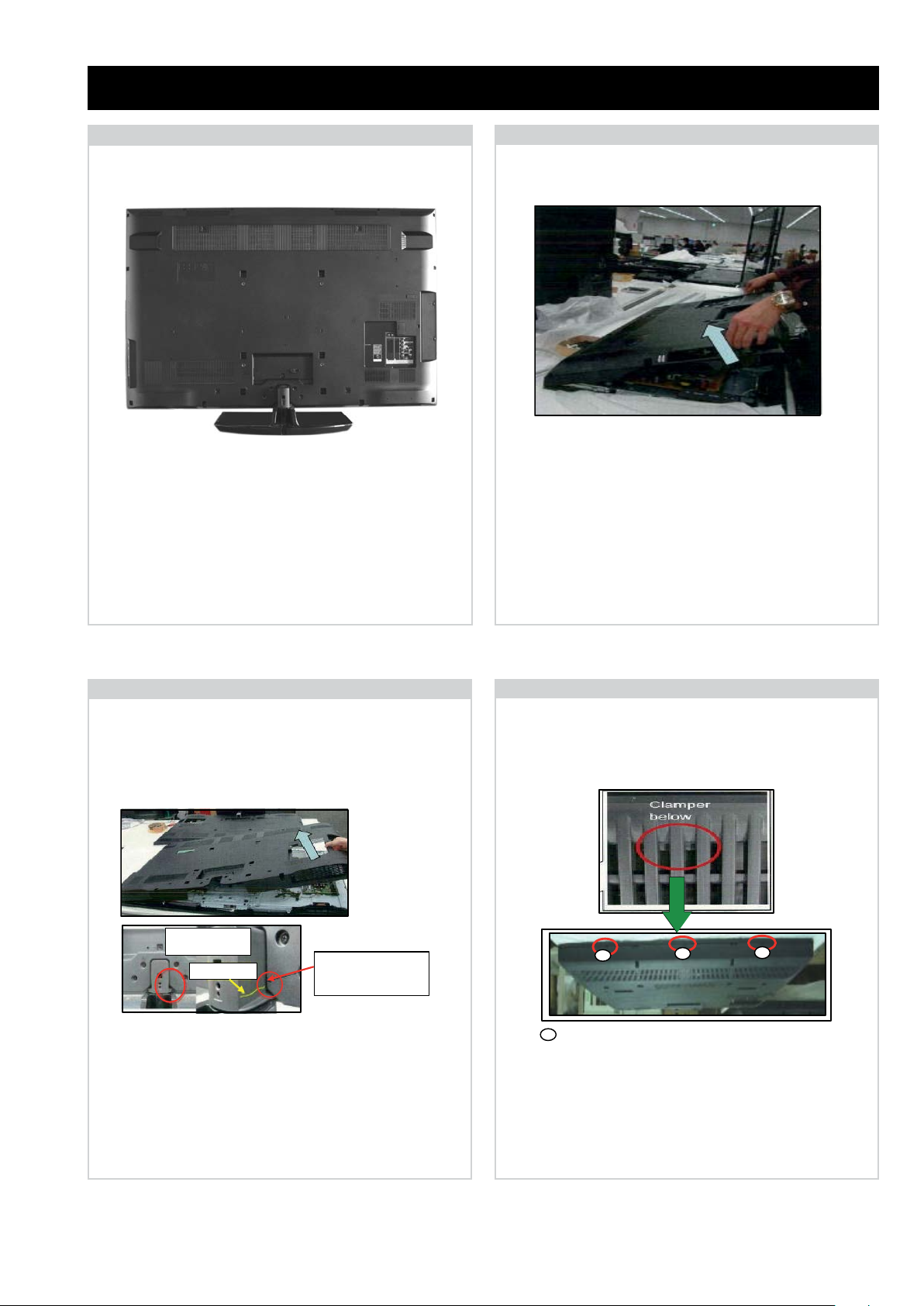
SECTION 2 DISASSEMBLY
Please pay attention
to operation trying not
to scratch stand neck.
Pay attention to
stand neck.
Scratch here
<TOP SIDE>
Clamper Point
2-1. Rear Cover Removal
=>
1
=>
3
=>
=>
=>
1
=>
3
3
=>
1
1
=>
1
=>
1
=>
1
=>
=>
3
3
=>
3
=>
1
3
=>
=>
1
Remove the rear cover fixing screws indicated and refer to
Sec 2-2-2(40/46 inches) or Sec 2-2-3(52 inches).
Screw Part number(s) and Description(s)
1) 2-580-640-01 SCREW, +BVTP2 4X16 (40/46” = 8pcs, 52” = 14pcs)
2) 7-685-648-79 SCREW, +BVTP 3X12 (40/46/52” = 2pcs)
3) 2-580-607-01 SCREW, +PSW M5X12 (40/46/52” = 7pcs)
=>
2
2-2. Rear Cover Removal (40/46 inches)
1
=>
1
=>
2
=>
1
=>
1
=>
1
=>
To remove the ‘Rear Cover’ lift the ‘Rear Cover’ from the
bottom to unlock the clamper.
2-3. Rear Cover Removal (52 inches)
To remove the ‘Rear Cover’ lift the ‘Rear Cover’ as shown
in the photo to unlock the clamper.
2-4. Rear Cover Installation (40/46 inches)
To install the ‘Rear Cover’ push the clamper points as
shown in the photo on the back surface of the ‘Rear Cover’
then replace all screws.
- 11 -
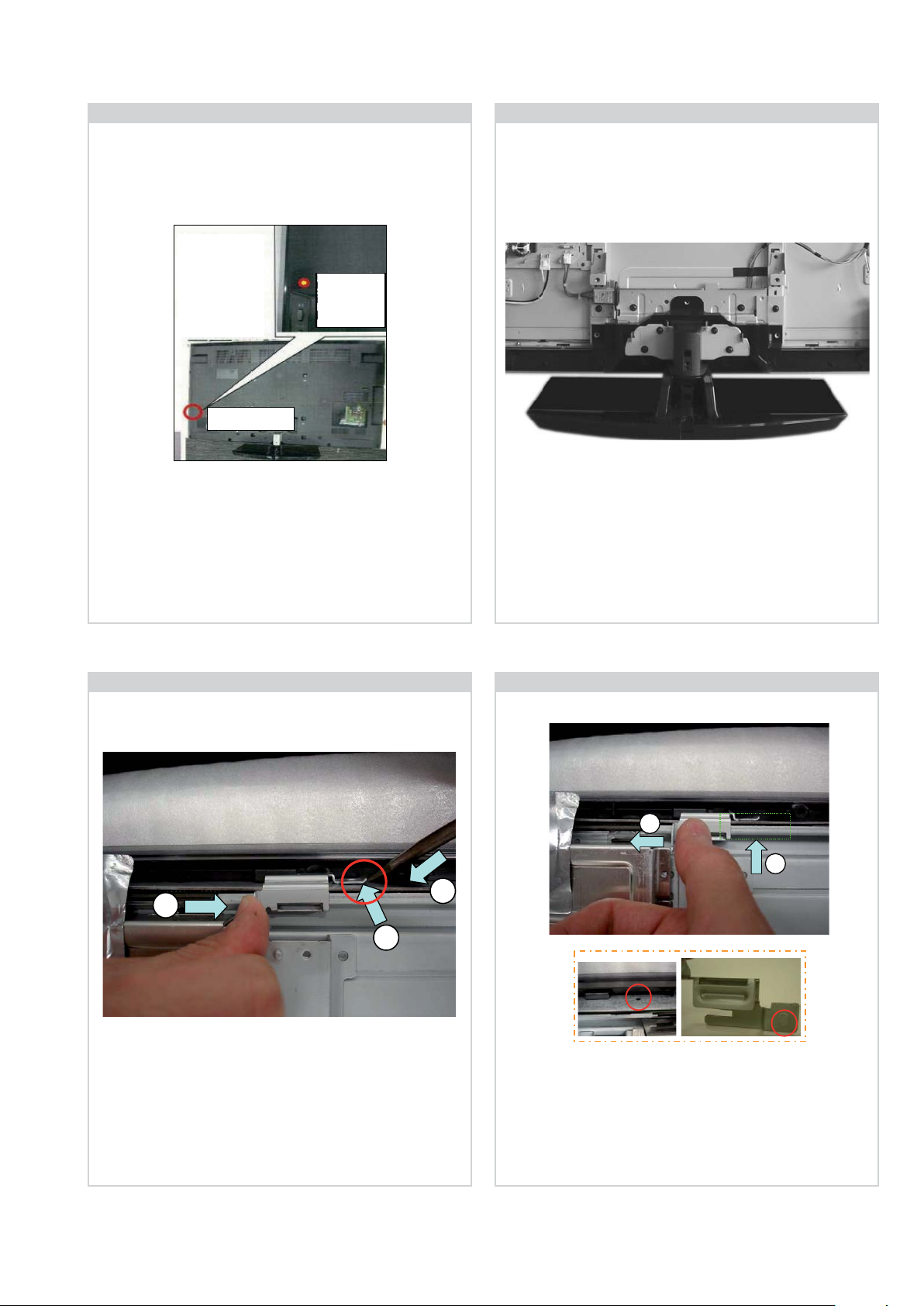
2-5. Rear Cover Installation (52 inches)
Clamper Here
Push This
Point
1
2
3
1
2
2-6. Stand Assy Removal
To install the ‘Rear Cover’ push the clamper point as shown
in the photo on the back surface of the ‘Rear Cover’ then
replace all screws.
2-7. Stay Top Removal
=>
=>
=>
=>
Remove the 4 stand fixing screws indicated and lift the TV
set up and away from the ‘Stand Assy’.
Screw Part number(s) and Description(s)
2-580-608-01 SCREW, +PSW M5X16
2-8. Stay Top Installation
To remove the ‘Stay Top’ place a flat blade screwdriver as
shown by 1 in the photo above, then lift the clamper slightly
as shown by 2 and finally slide the clamper as shown by 3.
When reusing the ‘Stay Top’ please use with the removed
set.
To install the ‘Stay Top’ slide into place as shown by 1 in the
photo above, then push the clamper as shown by 2, making
sure that the embossing on the clamper is locked in the hole
of the panel.
- 12 -
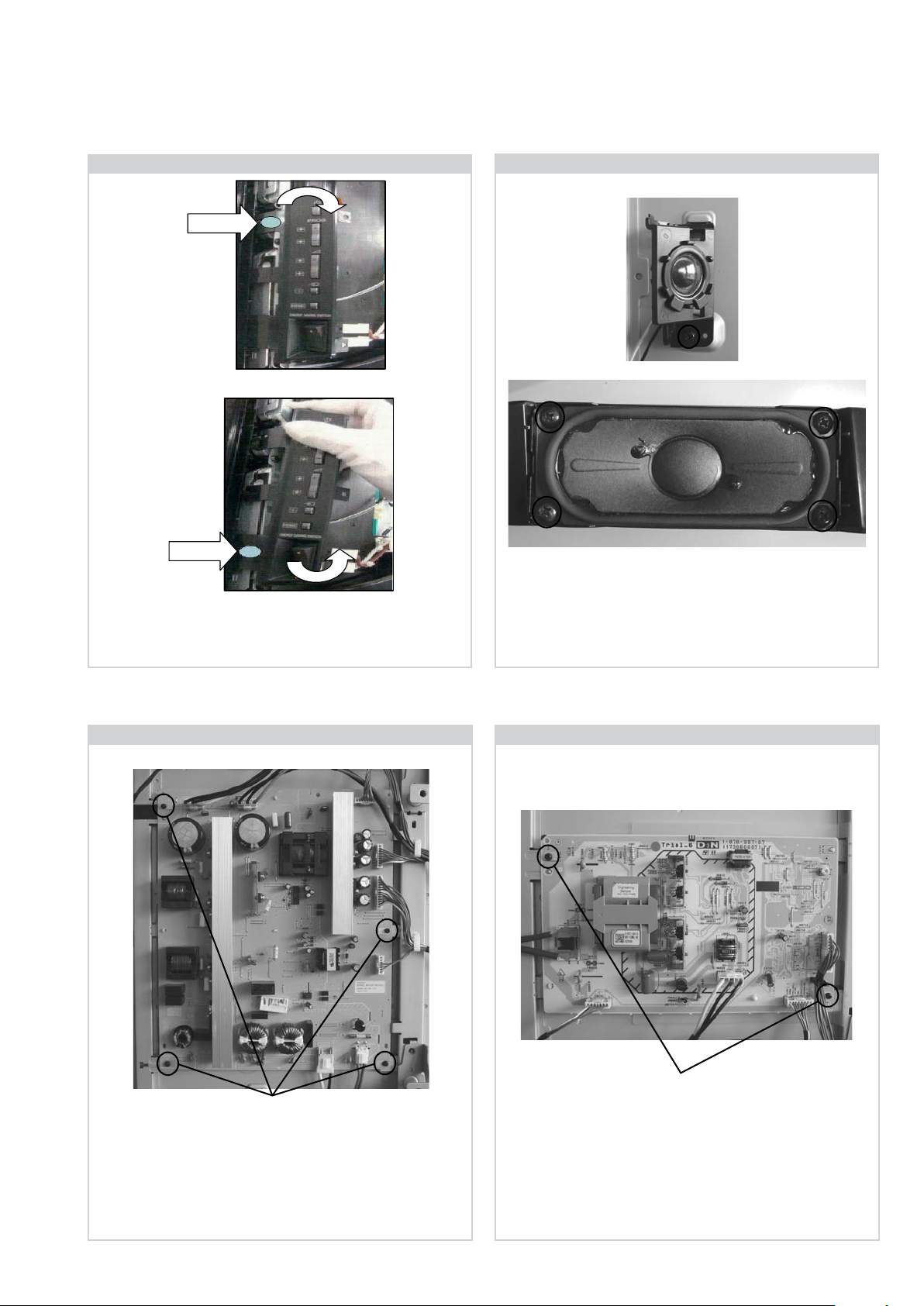
2-9. Switch Unit Removal
Push
Push
2-10. Loudspeaker Removal
a
To remove the ‘Switch Unit’ push the top of the unit in the
shaded area in the photo and rotate in the direction of the
arrow. Then repeat the procedure on the bottom of the unit.
2-11. G6NS/G7NS Board Removal
b
b
b
b
To remove the ‘Loudspeakers’ first disconnect the speaker
cables and then remove the screws circled.
Screw Part number(s) and Description(s)
(a) 2-580-592-01 SCREW, +PSW M3X8
(b) 2-580-640-01 SCREW, +BVTP2 4X16
2-12. D1N/D3N Board Removal
Screws
To remove the ‘G6NS/G7NS’ board disconnect all the
connectors and then remove the 4 screws circled and ease
the board gently away from the back of the TV set.
Screw Part number(s) and Description(s)
2-580-592-01 SCREW, +PSW M3X8
- 13 -
Screws
To remove the ‘D1N/D3N’ board disconnect all the
connectors and then remove the 2 screws circled and ease the
board gently away from the back of the TV set.
Note: Refer to page 4 - Hirose MDF61 connector.
Screw Part number(s) and Description(s)
2-580-592-01 SCREW, +PSW M3X8
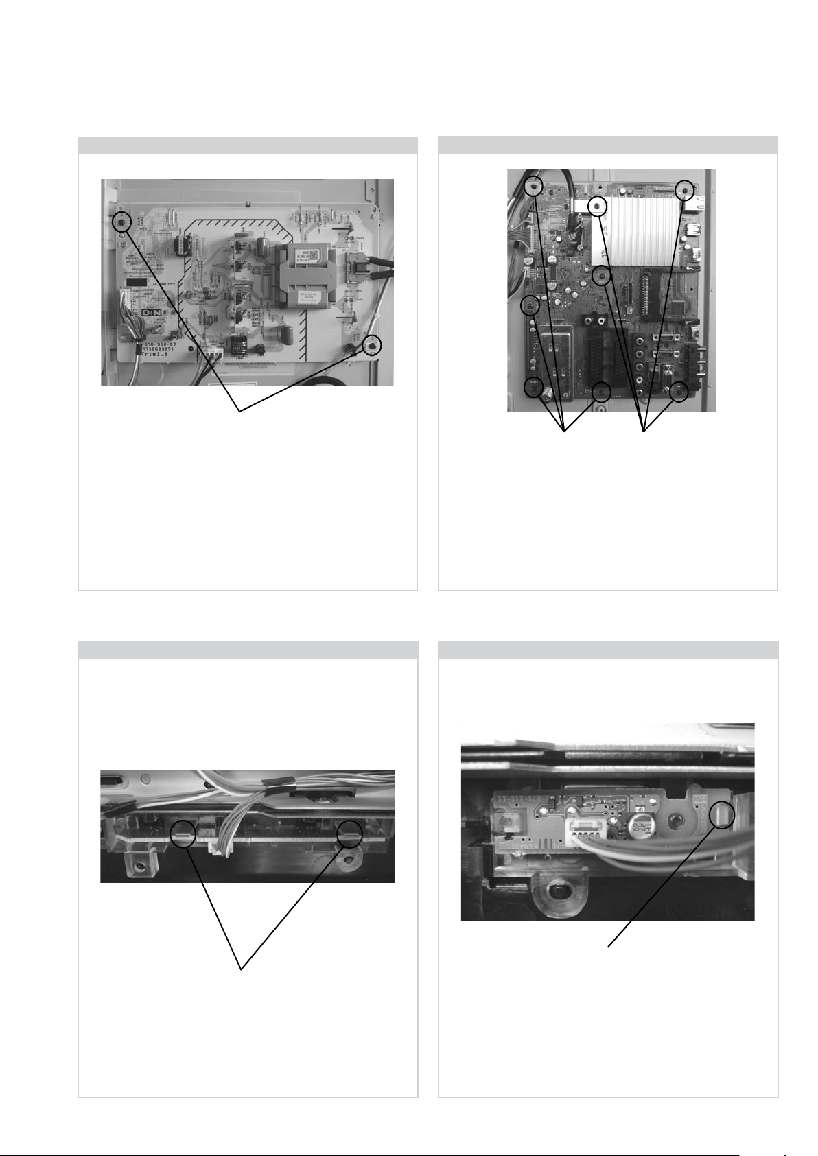
2-13. D2N/D4N Board Removal
Screws
2-14. BA Board Removal
Screws Screws
To remove the ‘D2N/D4N’ board disconnect all the
connectors and then remove the 2 screws circled and ease the
board gently away from the back of the TV set.
Note: Refer to page 4 - Hirose MDF61 connector.
Screw Part number(s) and Description(s)
2-580-592-01 SCREW, +PSW M3X8
2-15. HL1A Board Removal
To remove the ‘BA’ board disconnect all the connectors and
then remove the 8 screws circled and ease the board gently
away from the back of the TV set.
Screw Part number(s) and Description(s)
2-580-592-01 SCREW, +PSW M3X8
2-16. HSN Board Removal
Clips
To remove the ‘HL1A’ board disconnect the connector and
then release the 2 clips circled and ease the board gently
away from the back of the TV set.
Clip
To remove the ‘HSN’ board disconnect the connector and
then release the 1 clip circled and ease the board gently
away from the back of the TV set.
- 14 -
I/
TV
i+
5
+
(ON SCREEN (DIGIT 5) (VOLUME +) (TV)
DISPLAY)
(TV STANDBY)
(ON SCREEN
DISPLAY)
(DIGIT 5)
(VOLUME +)
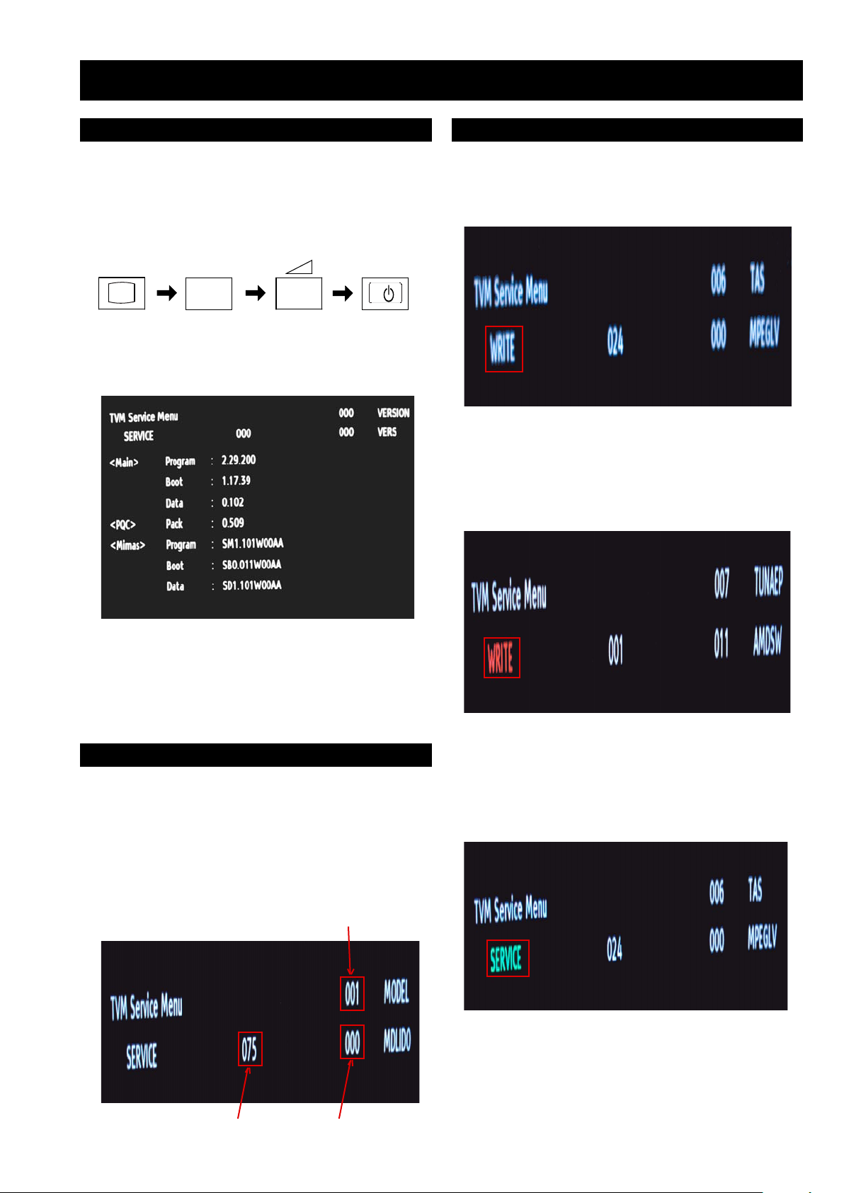
SECTION 3 SERVICE MENUS
3-1. How to enter the Service Mode
Service adjustments to this model can be performed using the
supplied Remote Commander RM-ED019.
1. Turn on the power to the TV set and enter into the stand-by
mode.
2. Press the following sequence of buttons on the Remote
Commander.
3. The TVM menu appears on the screen (See Pic.1).
Pic.1
3-3. Writing TVM Data
1. Press “Mute” on the remote commander. The word “SERVICE”
changes to “WRITE” (See Pic.3).
Pic.3
2. Press “0” on the remote commander. The word “WRITE”
changes to red. This indicates writing is in progess. (See Pic.4).
Pic.4
Note :
After carrying out the service adjustments, to prevent the
customer accessing the ‘Service Menu’ switch the TV set OFF
and then ON.
3-2. Changing TVM Data Settings
1. Press “2 / 5” on the remote commander to select (up / down)
category (See Pic.2).
2. Press “1 / 4” on the remote commander to select (up / down)
item (See Pic.2).
3. Press “3 / 6” on the remote commander to select (up / down)
data (See Pic.2).
Category
Pic.2
3. When red “WRITE” changes to green “SERVICE”.
This indicates writing is complete. (See Pic.5).
Pic.5
Data
Item
- 15 -
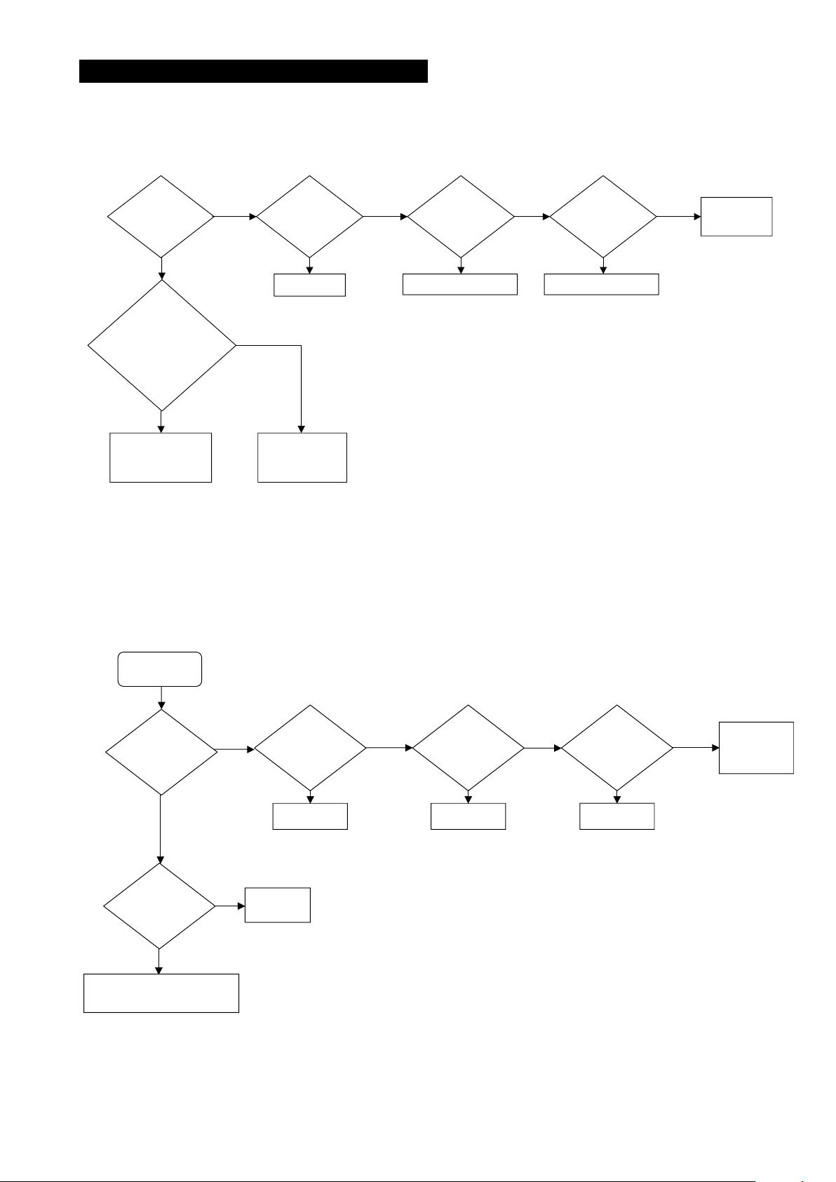
3-4. Trouble Shooting
Only?
Speaker Out
HDMI
Problem?
Analogue
Channel
Problem?
Digital
Channel
Problem?
BA Board
oNoNoNoN
Is UI of
Audio Setting
correct? Volume,
TV Speakers.
BA Board
BA Board or RF module BA Board or RF module
Confirm TV Settings,
reset using menu.
Check Speakers
or BA board.
No
Yes
Yes
3-4-1. FLOWCHART A
3-4-2. FLOWCHART B
BA Board
Video
Problem.
Do all Inputs
have a
problem?
HDMI
Problem?
Analogue
Channel
Problem?
Digital
Channel
Problem?
oNoNoNoN
BA Board
BA Board
BA Board
Check LVDS harness connection,
BA board, or Panel.
No
Yes
Yes
Is the Backlight
turned on?
BA Board
- 16 -
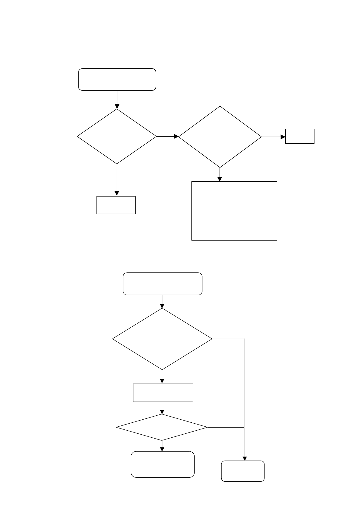
3-4-3. Flowchart C
Panel Problem
6,12,13,14 LED Blinks
Backlight
turned on?
connected
correctly?
No
Panel module or
G6NS(40") /
G7NS (46" , 52") / or
D1N ( 40" , 46" ) or'
D2N ( 40", 46") or
D3N (52") or D4N (52")
Yes
BA Board
LVDS
Yes
REPLACE PANEL
Finish
6 or 13 LED Blinks
NO
Replace (OK)
Replace (OK)
NO
D1N (40",46") or
D2N ( 40", 46") or
D3N (52") or
D4N (52")
BA BOARD
12 or 14 LED Blinks
3-4-4. Flowchart D
Is the
Is the LVDS
- 17 -
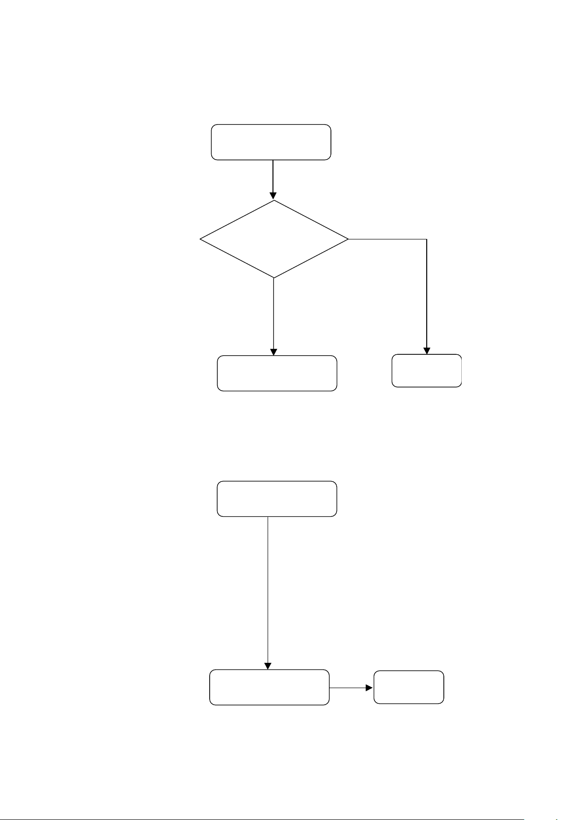
NO
Replace (OK)
Finish
2 LED Blinks
G6NS(40")/
G7NS(46",52")
Replace BA Board
Finish
5, 7 or 10 LED Blinks
Replace (OK)
3-4-5. Flowchart E
3-4-6. Flowchart F
Replace BA Board
- 18 -
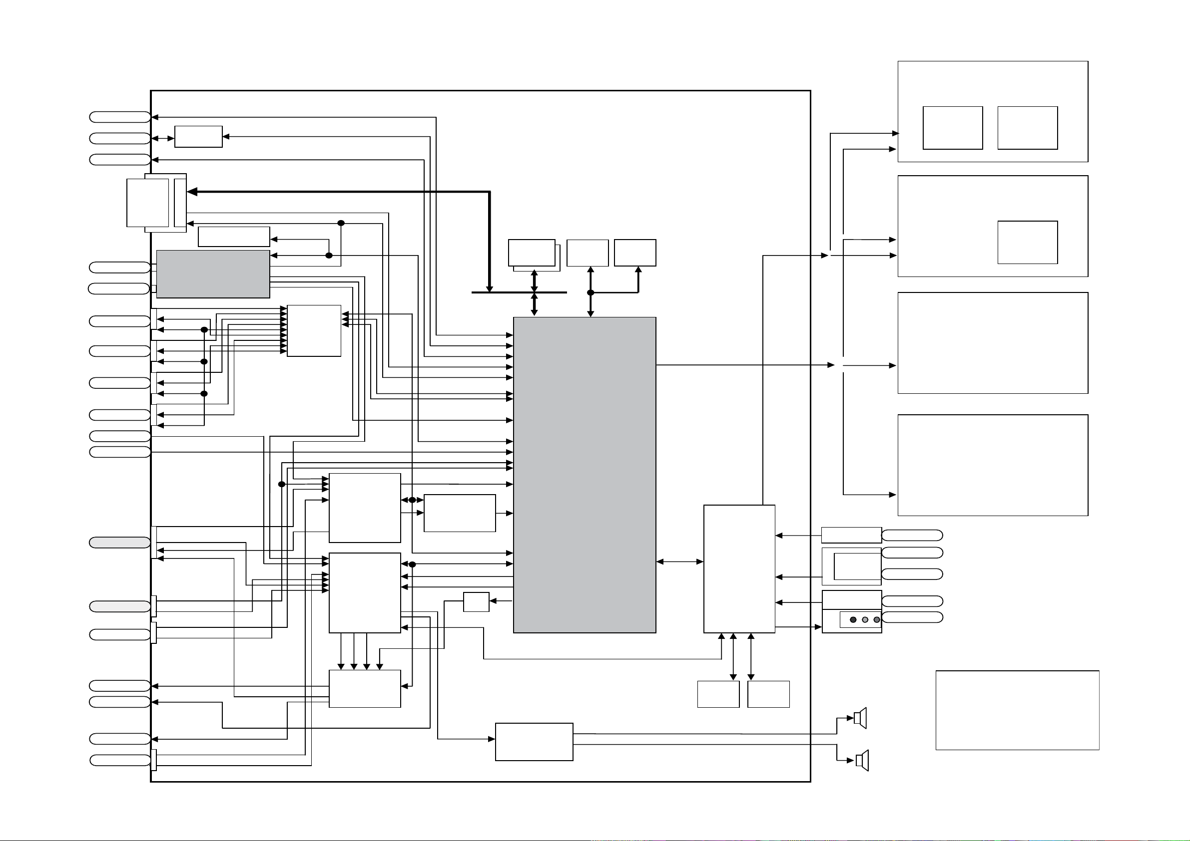
4-1. BLOCK DIAGRAM
EMMA3TL
Panel
240/200Hz
Power Supply
G6NS(40")/ G7NS
(46", 52") / D1N ( 40",
46" )/ D2N ( 40", 46")/
D3N (52") or D4N (52")
Aerial
Comp2
V1/MONout
Audio Out
Opt. Out
V2/Comp1
Tuner
USB
CI
PC In
PHY
MS (JIG)
Ether
SEIJI
CXA3785R
Audio
DSP
CXD9926
TAS
Video SW
CXA2241
DDR2
1Gb
MIMAS
Sub Chrom
SAA7115A
HDMI1
HDMI2
HDMI3
HDMI4
HDMI
EQ/SW
DDC
CEC
TMDS
DDC
CEC
TMDS
DDC
CEC
TMDS
DDC
CEC
TMDS
HP Out
CVBS/YCbCr
L/R
L/R
SPDIF
YCbCr
L/R
L/R
CVBS (SELOUT)
L/R (SELOUT)
CVBS/YC
RGB/HV
L/R
Amp
TAS5602
Side Video
YCbCr
L/R
SEL/MON
LO
HP
SPDIF
I2S 5.1ch
L/R
DAC
DDR2
512Mb
IIC1
IIC2
NVM
Temp
Sensor
UART
IIC
IIC
IIC
Power SW
Key
LOGO
IR
LED
HL1
SONY
HSN
PE-L PE-L
TS
TS
LVDS(60/50Hz)
IIC_SINK
NICAM/A2
IIC0
IIC
Panel
120/100Hz
PE-L
Panel
60/50Hz FHD
Panel
60/50Hz WXGA
NAND
512Mbx2
DVI/PC in
Cable
BA
- 19 -

5-2. CIRCUIT BOARD LOCATION
5-3. SCHEMATIC DIAGRAMS AND
PRINTED WIRING BOARDS
Note :
• All capacitors are in µF unless otherwise noted.
• pF : µµF 50WV or less are not indicated except for
electrolytic types.
• Indication of resistance, which does not have one for
rating electrical power, is as follows.
Pitch : 5mm
Electrical power rating : 1/4W
• Chip resistors are 1/10W
• All resistors are in ohms.
k = 1000 ohms, M = 1000,000 ohms
• : nonflammable resistor.
• : fusible resistor.
• : internal component.
• : panel designation or adjustment for repair.
• All variable and adjustable resistors have
characteristic curve B, unless otherwise noted.
• All voltages are in Volts.
• Readings are taken with a 10Mohm digital mutimeter.
• Readings are taken with a color bar input signal.
• Voltage variations may be noted due to normal production
tolerences.
• : B + bus.
• : B - bus.
• : RF signal path.
• : earth - ground.
• : earth - chassis.
Reference Information
RESISTOR RN
: METAL FILM
RC
: SOLID
FPRD
: NON FLAMMABLE CARBON
FUSE
: NON FLAMMABLE FUSIBLE
RS
: NON FLAMMABLE METAL OXIDE
RB
: NON FLAMMABLE CEMENT
RW
: NON FLAMMABLE WIREWOUND
: ADJUSTMENT RESISTOR
COIL LF-8L
: MICRO INDUCTOR
CAPACITOR TA
: TANTALUM
PS
: STYROL
PP
: POLYPROPYLENE
PT
: MYLAR
MPS
: METALIZED POLYESTER
MPP
: METALIZED POLYPROPYLENE
ALB
: BIPOLAR
ALT
: HIGH TEMPERATURE
ALR
: HIGH RIPPLE
Les composants identifiés par une trame et
par une marque sont d'une importance
critique pour la sécurité. Ne les remplacer
que par des pièces de numéro spécifié.
specified.
Note :
The components identified by shading
and marked are critical for safety.
Replace only with the part numbers
specified in the parts list.
Note :
CVM Board
A Board
S1 Board
VM
C
H
D1
A
J
A2
N
D
A1
D2
C
A
4-2. CIRCUIT BOARD LOCATION
D1N/D3N
BA
HSN
D2N/D4N
G6NS/G7NS
HL1A
4-3. SCHEMATIC DIAGRAMS AND
PRINTED WIRING BOARDS
Note :
The components identified by mark
confidential information.
Strictly follow the instructions whenever the
components are repaired and/or replaced.
contain
NOTE: The G7NS board is not a Sony board so it’s schematic diagram and printed wiring
board is not shown in this Service Manual.
Schematic diagrams are for reference only. Please refer to the electrical parts
list for the correct value and part number of components.
- 20 -

DDCCBB
O
P
EE
FF
Z
10
A B C D E F G H JI K L M N
1
2
3
4
5
6
7
8
9
1
2
3
4
5
6
7
8
9
11
10
11
22
21
22
R
Q
O
P
EE
FF
S
T
U
V
W
X
Y
Z
AA
BB
CC
DD
A B C D E F G H JI K L M N
12
13
14
15
16
17
18
19
20
21
20
18
19
17
15
16
14
12
13
Q R S T U V W X Y AA
XX
C7609
D3.3V
1005
25V
0. 0 1
X7R
C7605
1005
25V
0. 0 1
X7R
C7602
1005
25V
0. 0 1
X7R
C7603
R0XC-P
R0XC+P
R0X0-P
R0X0+P
R0X1-P
R0X1+P
R0X2-P
R0X2+P
DSCL0P
DSDA0P
1005
25V
0. 0 1
X7R
C7608
1005
25V
0. 0 1
X7R
C7604
10
*R7600
1k
*R7603
DDC_5V_1
5V_MAIN
1/16W
CHIP
10
R7601
5V_MAIN
DDC_5V_3
1k
R7604
1/16W
RN-CP
1k
*R7605
5V_MAIN
10
*R7602
DDC_5V_4
5V_MAIN
DDC_5V_S
1k
*R7607
10
*R7606
25V
0. 0 1
X7R
C7610
HDMI_CE
25V
0. 0 1
X7R
C7607
1005
25V
0. 0 1
X7R
C7606
R0PWR5V_1
XX
R7619
1005
25V
0. 0 1
X7R
C7600
1005
25V
0. 0 1
X7R
C7601
4. 7 k
R7612
5V_MAIN
EMI
FL7600
D7603
XX
D7604
XX
D7605
XX
D7607
XX
XX
R7617
XX
R7618
5V_MAIN
XX
R7614
25V
0. 0 1
X7R
C7611
8 7 6 5
4321
M24C02-WMN6T(B)
IC7601
A1
A0
A2
E SDA
SCL
WP
VCC
16V
0.1
C7612
XX
R7623
XX
R7620
1/16W
CHIP
10k
R7621
5%
D3.3V
DDC_5V_S
DDC_5V_4
DDC_5V_3
DDC_5V_1
100
*RB7607
100
*RB7602
100
RB7601
100
*RB7600
SCL2
SDA2
CL7600
CL7601
CL7602
CL7603
XX
RB7609
10k
RB7606
EQ_MVCC
EQ_MVCC
GND_D
CEC_OUT
1/16W
CHIP
5%
27k
R7624
1005CHIP
R7622
0
CEC_IN CEC
JL7600
XX
C7613
STBY_3.3V
1 2 3
456
IC7602
XX
CEC_IN
CEC_OUT
VCC A
GND
B
CEC
D7609
MA2SD320G8S0
2. 2 k
RB7610
VD7622
XX
VD7623
XX
VD7604XXVD7607
XX
VD7601
XX
VD7620
XX
VD7621
XX
VD7603
XX
VD7606
XX
VD7600
XX
VD7624
XX
VD7625
XX
VD7605XXVD7608
XX
VD7602
XX
VD7626
XX
VD7627
XX
VD7615
XX
VD7616XXVD7617
XX
D7608
MA2SD320G8S0
100
*R7608
100
R7609
100
*R7610
100
*R7611
1k
R76271kR7628
1k
R7626
XX
R7631
XX
R7630
XX
R7632
XX
R7629
10k
R7634
16V
0.1
C7614
6.3V1
C7615
47k
*RB7605
47k
RB7604
47k
*RB7603
214
3
47k
*RB7608
1
2
3
4
8
7
6
5
0uH
*L7600
1
2
3
4
8
7
6
5
0uH
*L7601
1
2
3
4
8
7
6
5
0uH
L7602
1
2
3
4
8
7
6
5
0uH
L7603
1
2
3
4
8
7
6
5
0uH
*L7604
1
2
3
4
8
7
6
5
0uH
*L7605
1
2
3
4
8
7
6
5
0uH
*L7606
1
2
3
4
8
7
6
5
0uH
*L7607
0
*R7635
CHIP
0
R7636
0
*R7637
0
*R7638
JL7601
JL7602
JL7603
1/16W
CHIP
5%
100
R7625
1 2 3 4 5 6 7 8 9 10 11 12 13 14 15 16 17 18 19 20 21 22 23 24 25
26
27
28
29
30
31
32
33
34
35
36
37
38
39
40
41
42
43
44
45
46
47
48
49
50
51525354555657585960616263646566676869707172737475
76
77
78
79
80
81
82
83
84
85
86
87
88
89
90
91
92
93
94
95
96
97
98
99
100
IC7600
CXB1447R-T6
SCL_D
GND
DCLKN
DCLKP
VCC
DDT0N
DDT0P
GND
DDT1N
DDT1P
VCC
DDT2N
DDT2P
GND
GPI-1
GPI-2
GPI-3
GPI-4
DDC5V_A
DDC5V_B
DDC5V_C
DDC5V_D
MVCC
DVCC
GND
EWP
SCL_E
SDA_E
SCL_M
SDA_M
ADD
REFRESH
CE
REXT
GND
ZP
ZN
VCC
YP
YN
GND
XP
XN
VCC
WP
WN
GND
SCL_SINK
SDA_SINK
DDC5V_MOUT
HPD_A
SDA_A
SCL_A
VCC
ACLKN
ACLKP
VCC
ADT0N
ADT0P
GND
ADT1N
ADT1P
VCC
ADT2N
ADT2P
GND
HPD_B
SDA_B
SCL_B
BCLKN
BCLKP
VCC
BDT0N
BDT0P
GND
GND
BDT1N
BDT1P
VCC
BDT2N
BDT2P
GND
HPD_C
SDA_C
SCL_C
GND
CCLKN
CCLKP
VCC
CDT0N
CDT0P
GND
CDT1N
CDT1P
VCC
CDT2N
CDT2P
GND
HPD_D
SDA_D
*CN7600
1D2+
2E
3D2-
4D1+
5E
6D1-
7D0+
8E
9DO-
10CLK+
11E
12CLK-
13CEC
14NC
15DDC CLK
16DDC DAT
17E
18DDC +5V
19HPD
20
20P
CN7601
1D2+
2E
3D2-
4D1+
5E
6D1-
7D0+
8E
9DO-
10CLK+
11E
12CLK-
13CEC
14NC
15DDC CLK
16DDC DAT
17E
18DDC +5V
19HPD
20
*CN7602
D2+
2E
3D2-
4D1+
5E
6D1-
7D0+
8E
9D0-
10CLK+
11E
12CLK-
13CEC
14NC
15DDC CLK
16DDC DAT
17E
18DDC +5V
19HPD
20
*CN7603
D2+
2E
3D2-
4D1+
5E
6D1-
7D0+
8E
9D0-
10CLK+
11E
12CLK-
13CEC
14NC
15DDC CLK
16DDC DAT
17E
18DDC +5V
19HPD
20
1/16W
CHIP
5%
47k
R7613
RX2_3R-
RX1_3RRX1_3R+
RX2_3R+
RXC_2R-
RX1_2R-
RX2_2R-
RXC_2R+
RX0_2R-
RX0_2R+
RX1_2R+
RX2_2R+
RXC_4R-
RXC_1R-
RXC_1R+
RX0_1R-
RX0_1R+
RX2_1R-
RX2_1R+
RX1_1R+
RX1_1R-
RXC_4R+
RX0_4RRX0_4R+
RX1_4RRX1_4R+
RXC_3R-
RXC_3R+
RX0_3R-
RX0_3R+
RX2_4R-
RX2_4R+
RX0_1R-
RX1_1R+
RX2_1R+
RXC_3R+
RX0_3R+
RX1_3R+
RX2_3R-
RXC_4R-
RX0_4R-
RX1_4R-
RX2_4R-
RXC_2R+
RX0_2R+
RX2_2R-
RX1_2R-
RXC_1R-
RXC_1R+
RX0_1R+
RX1_1R-
RX2_1R-
RXC_3R-
RX0_3R-
RX1_3R-
RX2_3R+
RXC_4R+
RX0_4R+
RX1_4R+
RX2_4R+
RXC_2R-
RX0_2R-
RX1_2R+
RX2_2R+
HDMI1
TOP
HDMI2
TOP
HDMI4
SIDE
HDMI3
SIDE
input D
input C
input B
input A
[q†«•o
00'RlN^–
CEC
TO HDMI JACK
TO MAIN MAICON
RB7609i”¯p^[–•Ø
BA-EX2L
COMPONENTS MARKED AS XX REFER TO PARTS LIST, WILL ONLY BE LISTED IF FITTED
BA
1/18 TUNER, MAIN MICROCONTROLLER, HDMI/AV SIDE/PC INPUT, SCARTS
- 21 -
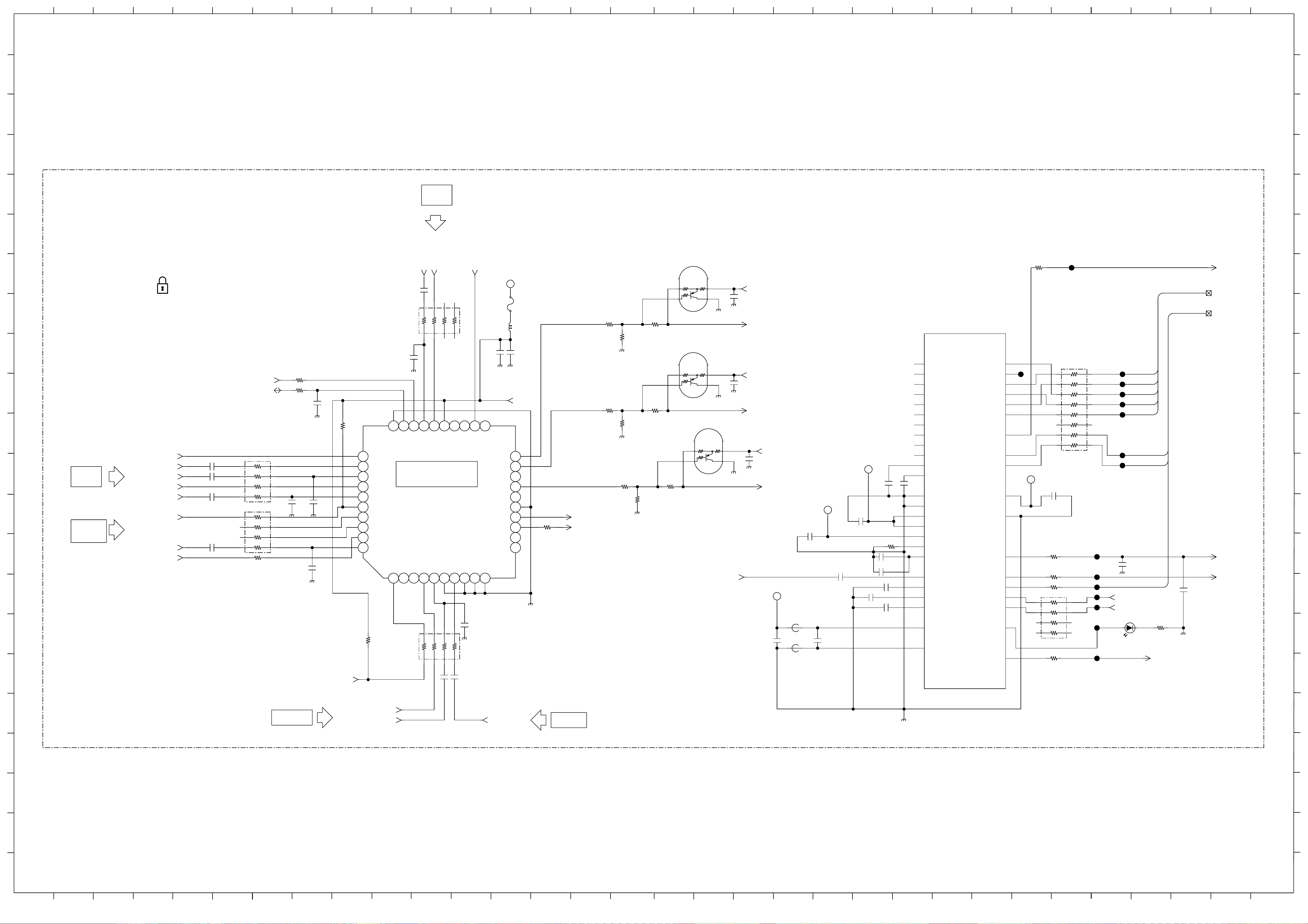
~ BA Board Schematic Diagram [ Tuner, Main Microcontroller, HDMI/AV Input/PC Input, Scarts ] Page 1/18 ~
DDCCBB
O
P
EE
FF
Z
10
A B C D E F G H JI K L M N
1
2
3
4
5
6
7
8
9
1
2
3
4
5
6
7
8
9
11
10
11
22
21
22
R
Q
O
P
EE
FF
S
T
U
V
W
X
Y
Z
AA
BB
CC
DD
A B C D E F G H JI K L M N
12
13
14
15
16
17
18
19
20
21
20
18
19
17
15
16
14
12
13
Q R S T U V W X Y AA
5.6k
R4203
XX
R4211
GND_D
VSW_A5.0V
SCL2
XX
C4206
GND_D
VSW_A5.0V
CVBS_FRONT
100
RB4201
2
1
4
3
6
5
8
7
R4207
10k
5.6k
R4204
100
RB4204
CVBS_VIDEO1
XX
R4212
GND_D
1 2 3 4 5 6 7 8 9 10
11
12
13
14
15
16
17
18
19
20
21222324252627282930
31
32
33
34
35
36
37
38
39
40
CXA2241Q-T4
IC4200
S2_1
C2
Y2
S1_1
V2
GND
V1
NC
NC
OUT3
NC
COUT3
V/YOUT3
VOUT3
NC
COUT2
V/YOUT2
NC
COUT1
V/YOUT1
NC
S2_4
C5
Y5
Vcc
S1_4
V5
SCL
SDA
ADR
S2_3
C4
Y4
S1_3
V4
S2_2
C3
Y3
S1_2
V3
R4208
10k
GND_D
5V_MAIN
GND_D
GND_D
16V
0.1
C4213
22uH
L4200
1608
10V
1
X7R
C4209
RT3S02M-T111-1
Q4200
3 2 1
654
RT3S02M-T111-1
Q4201
3 2 1
654
1
C4205
1
C4210
1
C4211
R4200
0
R4202
0
GND_D
VSW_A5.0V
R4209
XX
100
R4205
RT3S02M-T111-1
Q4202
3 2 1
654
VSW_A5.0V
100
RB4200
2
1
4
3
6
5
8
7
1
C4202
1
C4201
1
C4200
RF_ANALOG_CV
Y_VIDEO1
C_SCART2
CVBS_SCART1
MODE1
MODE2
V1_DET SUB_CV/Y
BAVI00
BAVI35
A_REC/MON_OUT_CVCOMP1_DET
COMP2_DET
SIDE_V_DET/V2_DET
100
RB4203
SDA2
PC_DET
100
R4201
XX
R4213
10V
4.7
C4214
X7R
2012
RF_DIGITAL_CV
XX
C4217
XX
C4218
XX
C4219
GND_D
GND_D
GND_D
V1_S_SW
R4218
10k
R4217
10k
TV_OUT
0
*R4216
XX
C4223
GND_D
XX
C4222
GND_D
XX
C4220
GND_D
GND_D
XX
C4221
GND_D
XX
C4224
36V
1.4A
F4200
Video SW
RF
YC:Digital
CV:Analog
AV2/
VIDEO1
SIDE_CVBS
AV1/
VIDEO3
Digital_RF
BA-EX2L
COMPONENTS MARKED AS XX REFER TO PARTS LIST, WILL ONLY BE LISTED IF FITTED
BA
2/18
47
R5020
1/16W
CHIP 5%47
R5023
1/16W
CHIP 5%47
R5025
1/16W
CHIP 5%47
R5024
SPDIF_IN
016:2B
016:2C
016:2I
SIFIN
019:3F;022:7C
CL5011
CL5012
CL5013
CL5014
CL5015
CL5016
CL5017
CL5018
CL5019
CL5020
CL5021
CL5022
CL5023
CL5024
CL5025
FE_MCK
016:2C
SUB_MCK
016:2I
CL5027
D3.3V
D1.5V
A3.3V
0.1
C5004
0.1
C5005
GND_D
D3.3V
0.1
C5007
XX
R5050
0.1
C5009
0.1
C5010
0.1
C5011
1005
16V
0.1
C5012
XX
C5023
XX
C5024
X_HDMI_INT
016:2E
XX
C5008
XX
C5013
GND_D
SML-310MTT86
*D5000
XX
1005
1/16W
CHIP
5%
*R5026
XX
AFT_UP
022:17G
AFT_DN
022:15C;022:17G
47
RB5000
2
1
4
3
6
5
8
7
10
9
12
11
14
13
16
15
1/16W
CHIP
5%
47
R5051
XX
C5025
XX
C5026
GND_D
47
RB5001
2
1
4
3
6
5
8
7
MC-10144F1-410-LU2-A
*IC2001
AAIL0
B6
AAIR0
C6
AAIL1
A5
AAIR1
B5
AAIL2
A4
AAIR2
B4
AAIL3
C8
AAIR3
C7
AAIL4
C5
AAIR4
D7
AAILC
D6
AAIRC
D5
AAIAG33L
C4
AAIAG33R
D4
AAIAV33L
E6
AAIAV33R
E5
AAIDV15
F5
AAIIREF
E4
AAIREG
E7
SIFIN
A7
SIFVCOM
A6
SIFVRB
E8
SIFVRT
F7
SIFAVDD33
B7
SIFAGND
A8
MAAOL0
A2
MAAOR0
B1
MAAOL1
B3
MAAOR1
C3
MAAOL2
B2
MAAOR2
C1
MAO958
H5
SAAOL0
C2
SAAOR0
D2
AAO0DV33
D3
AAO0DG
A3
GPIO65/MAOMCK
M6
GPIO64/SAOMCK
M5
GPIO72/SAO0BCK
P4
GPIO67/SAO1LRCK
P5
GPIO68/SAO1D0
N4
GPIO66/SAO1BCK
N6
GPIO9/MUTE
K4
1005
16V
0.1
C5027
0uH
FB5000
0uH
FB5001
0.1
C5006
FE_LRCK
FE_BCK
FE_DATA1
SUB_DATA
SUB_BCK
SPDIF_IN
SUB_LRCK
FE_DATA3
FE_DATA2
Portion9
- 22 -
~ BA Board Schematic Diagram [ Tuner, Main Microcontroller, HDMI/AV Input/PC Input, Scarts ] Page 2/18 ~
 Loading...